Embed Size (px)
Citation preview


ii
Dedication
To my lovely wife
iii
Acknowledgements
My Ph.D. dissertation work would not be successful without the
contributions from many people. I would like to thank them there.
First of all, I would like to thank Professor Martin Reiser for his
professional advice and guidance during my tenure as a graduate student. His
enthusiasm and encouragement have greatly motivated me to finish my Ph.D.
work. I would also like to thank Dr. JG Wang for his tremendous help in both the
theoretical and experimental part of my dissertation. I would like to thank
Professor Patrick O'Shea. He became my co-advisor at the final stage of my Ph.D.
project and has contributed with valuable advice and criticism to my work. I would
like to express my thanks to Dr. Rami Kishek, the assistant manager for UMER, for
useful discussions. I am thankful to Dr. Santiago Bernal for his valuable help in my
experiment and in the final polishing of my dissertation. I would like to thank Dr.
Hyyong Suk, the former graduate student whose work I continued, for transferring
his knowledge of the facility and of the resistive-wall experiment to me. I am also
grateful to Victor Yun, who, with his professional expertise, provided invaluable
help in the mechanical design of the energy analyzer and the BPMs.
I am also grateful to Prof. Chuan Liu, Prof. Derek Boyd, Prof. Jon Orloff
for serving on the advisory committee. I would thank Dr. Irving Haber at NRL,
Drs. David Kehne and Terry Godlove at FMT for their helpful advice and
iv
discussions about the resistive-wall experiment and the development of the
diagnostic tools.

v
Table of Contents
Section Page
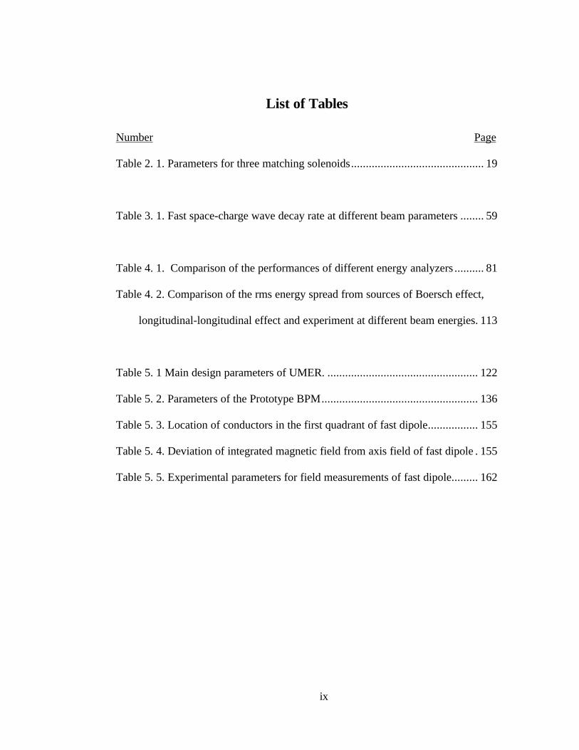
List of Tables........................................................................................................ ix
List of Figures........................................................................................................ x
Chapter 1 Introduction .......................................................................................... 1
1.1 Historical Background ................................................................................. 1
1.2 Terminology and Basic Theory of Beam Physics ......................................... 4
1.2.1 K-V (Kapchinsky-Vladimirsky) Distribution....................................... 4
1.2.2 Beam Emittance.................................................................................. 6
1.3 Organization of the Dissertation................................................................... 8
Chapter 2 Facility for the Resistive-Wall Instability Experiments.......................... 9
2.1 Experimental Setup...................................................................................... 9
2.2 Electron Gun ............................................................................................... 9
2.3 Matching Lenses and Long Solenoid Transport ......................................... 17
2.4 Resistive-Wall Tubes................................................................................. 27
2.5 Diagnostics ................................................................................................ 27
2.6 Vacuum System......................................................................................... 29
Chapter 3 Space-Charge Waves in Electron Beams Propagating Through a
Resistive-Wall Channel........................................................................................ 31
3.1 Motivation ................................................................................................. 31

vi
3.2 Linear Theory on the Resistive-Wall Instability ......................................... 34
3.2.1 Resistive-Wall Instability Theory Based on One-dimensional Model
and Vlasov Equation. ........................................................................ 34
3.2.2 Space-Charge Waves in a Monoenergetic Electron Beam With
Conducting, Resistive and Complex Wall Impedance........................ 37
3.2.3 Landau Damping............................................................................... 45
3.3 Experimental Study of the Resistive-Wall Instability ................................. 46
3.3.1 Generation of Space Charge Waves................................................... 46
3.3.2 Beam Matching into the Resistive-Wall Channel............................... 50
3.3.3 Experiments of Space-Charge Waves in the Linear Regime .............. 53
3.3.4 Experiments with Fast Waves in the Nonlinear Regime [43] ............. 61
3.4 Summary ................................................................................................... 69
Chapter 4 Development of a High-Performance Retarding Field Energy Analyzer
............................................................................................................................ 70
4.1 Introduction ............................................................................................... 70
4.2 Theory of Retarding Field Energy Analyzer............................................... 71
4.3 Design of a Compact, High-Performance Energy Analyzer........................ 81
4.4 Beam Test of the New Energy Analyzer .................................................... 91
4.4.1 Electron Gun Commissioning ........................................................... 91
4.4.2 Experimental Apparatus.................................................................... 93
4.4.3 Test Results ...................................................................................... 94

vii
4.5 Theoretical Considerations of the Sources of Beam Energy Spread.......... 104
4.5.1 The Boersch Effect ......................................................................... 104
4.5.2 The Longitudinal-Longitudinal Relaxation Effect ........................... 110
4.5.3 Comparison of the Experimental Results with the Energy Spread
Predicted by the above two Sources. ............................................... 112
4.6 A Computer-Controlled System for Energy Spread Measurements .......... 114
4.7 Conclusion and Future Work ................................................................... 118
Chapter 5 Development of a Capacitive Beam Position Monitor (BPM) and a Fast
Rise-Time Dipole for the University of Maryland Electron Ring (UMER) ......... 120
5.1 The University of Maryland Electron Ring (UMER)................................ 120
5.2 Development of a Capacitive Beam Position Monitor (BPM) .................. 123
5.2.1 Motivation ...................................................................................... 123
5.2.2 Basic Principle ................................................................................ 124
5.2.3 Design and Bench Test of a Prototype BPM.................................... 134
5.2.4 BPM Data Acquisition and Electronics ........................................... 143
5.3 Study of a Fast Rise-time Deflecting Dipole ............................................ 150
5.3.1 Motivation ...................................................................................... 150
5.3.2 Basic Configuration ........................................................................ 151
5.3.3 Inductance and Magnetic Field Measurement of a Prototype Model 157
5.4 Summary ................................................................................................. 169
Chapter 6 Conclusion........................................................................................ 170
viii
Appendix I Study the Higher Order Term of BPM Responses to Beam Position 173
Appendix II Estimating the Inductance of the Fast Dipole................................. 177
References ......................................................................................................... 179
ix
List of Tables
Number Page
Table 2. 1. Parameters for three matching solenoids............................................. 19
Table 3. 1. Fast space-charge wave decay rate at different beam parameters ........ 59
Table 4. 1. Comparison of the performances of different energy analyzers .......... 81
Table 4. 2. Comparison of the rms energy spread from sources of Boersch effect,
longitudinal-longitudinal effect and experiment at different beam energies. 113
Table 5. 1 Main design parameters of UMER. ................................................... 122
Table 5. 2. Parameters of the Prototype BPM..................................................... 136
Table 5. 3. Location of conductors in the first quadrant of fast dipole................. 155
Table 5. 4. Deviation of integrated magnetic field from axis field of fast dipole . 155
Table 5. 5. Experimental parameters for field measurements of fast dipole......... 162
x
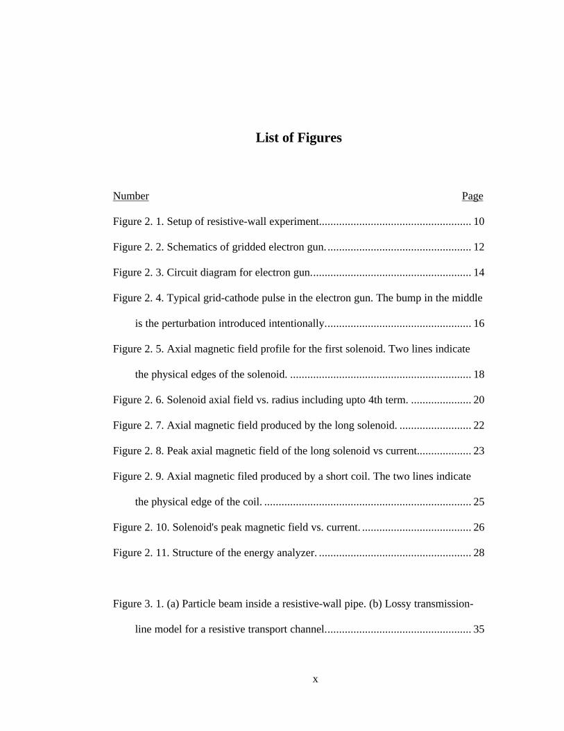
List of Figures
Number Page
Figure 2. 1. Setup of resistive-wall experiment..................................................... 10
Figure 2. 2. Schematics of gridded electron gun. .................................................. 12
Figure 2. 3. Circuit diagram for electron gun........................................................ 14
Figure 2. 4. Typical grid-cathode pulse in the electron gun. The bump in the middle
is the perturbation introduced intentionally................................................... 16
Figure 2. 5. Axial magnetic field profile for the first solenoid. Two lines indicate
the physical edges of the solenoid. ............................................................... 18
Figure 2. 6. Solenoid axial field vs. radius including upto 4th term. ..................... 20
Figure 2. 7. Axial magnetic field produced by the long solenoid. ......................... 22
Figure 2. 8. Peak axial magnetic field of the long solenoid vs current................... 23
Figure 2. 9. Axial magnetic filed produced by a short coil. The two lines indicate
the physical edge of the coil. ........................................................................ 25
Figure 2. 10. Solenoid's peak magnetic field vs. current. ...................................... 26
Figure 2. 11. Structure of the energy analyzer. ..................................................... 28
Figure 3. 1. (a) Particle beam inside a resistive-wall pipe. (b) Lossy transmission-
line model for a resistive transport channel................................................... 35
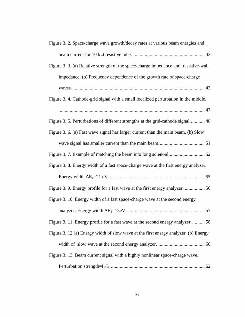
xi
Figure 3. 2. Space-charge wave growth/decay rates at various beam energies and
beam current for 10 kΩ resistive tube........................................................... 42
Figure 3. 3. (a) Relative strength of the space-charge impedance and resistive-wall
impedance. (b) Frequency dependence of the growth rate of space-charge
waves........................................................................................................... 43
Figure 3. 4. Cathode-grid signal with a small localized perturbation in the middle.
.................................................................................................................... 47
Figure 3. 5. Perturbations of different strengths at the grid-cathode signal............ 48
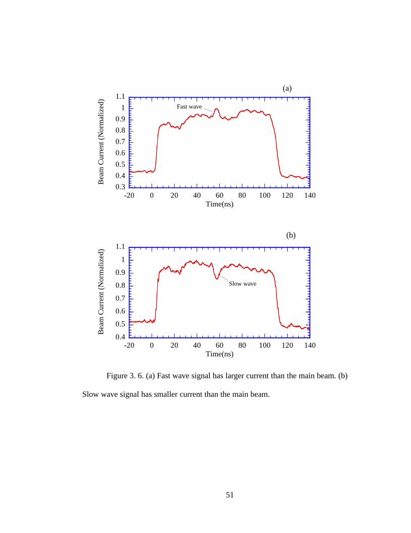
Figure 3. 6. (a) Fast wave signal has larger current than the main beam. (b) Slow
wave signal has smaller current than the main beam..................................... 51
Figure 3. 7. Example of matching the beam into long solenoid............................. 52
Figure 3. 8. Energy width of a fast space-charge wave at the first energy analyzer.
Energy width ∆E1=21 eV. ............................................................................ 55
Figure 3. 9. Energy profile for a fast wave at the first energy analyzer. ................ 56
Figure 3. 10. Energy width of a fast space-charge wave at the second energy
analyzer. Energy width ∆E2=13eV. .............................................................. 57
Figure 3. 11. Energy profile for a fast wave at the second energy analyzer. .......... 58
Figure 3. 12 (a) Energy width of slow wave at the first energy analyzer. (b) Energy
width of slow wave at the second energy analyzer....................................... 60
Figure 3. 13. Beam current signal with a highly nonlinear space-charge wave.
Perturbation strength=Ip/Ib............................................................................ 62
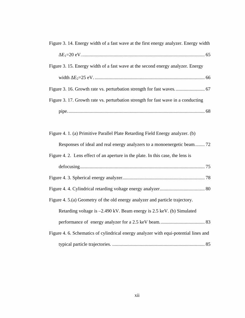
xii
Figure 3. 14. Energy width of a fast wave at the first energy analyzer. Energy width
∆E1=20 eV................................................................................................... 65
Figure 3. 15. Energy width of a fast wave at the second energy analyzer. Energy
width ∆E2=25 eV. ........................................................................................ 66
Figure 3. 16. Growth rate vs. perturbation strength for fast waves. ....................... 67
Figure 3. 17. Growth rate vs. perturbation strength for fast wave in a conducting
pipe.............................................................................................................. 68
Figure 4. 1. (a) Primitive Parallel Plate Retarding Field Energy analyzer. (b)
Responses of ideal and real energy analyzers to a monoenergetic beam........ 72
Figure 4. 2. Lens effect of an aperture in the plate. In this case, the lens is
defocusing.................................................................................................... 75
Figure 4. 3. Spherical energy analyzer.................................................................. 78
Figure 4. 4. Cylindrical retarding voltage energy analyzer.................................... 80
Figure 4. 5.(a) Geometry of the old energy analyzer and particle trajectory.
Retarding voltage is –2.490 kV. Beam energy is 2.5 keV. (b) Simulated
performance of energy analyzer for a 2.5 keV beam. ................................... 83
Figure 4. 6. Schematics of cylindrical energy analyzer with equi-potential lines and
typical particle trajectories. .......................................................................... 85
xiii
Figure 4. 7. Beam trajectories at different retarding voltages. Beam energy is 2.500
keV. (a). Retarding voltage is 2.4994 keV. (b) Retarding voltage is 2.4997
keV. (c). Retarding voltage is 2.500 keV...................................................... 87
Figure 4. 8. Simulation shows that, for the beam with divergence angle of 5o, the
old one has resolution of 20eV, while the new one has resolution of 0.6eV. . 88
Figure 4. 9. Energy analyzer responses to a monogenetic beam at different beam
energy of 2.5 keV, 5.5 keV and 10 keV........................................................ 89
Figure 4. 10. Cross Section of new energy analyzer with cylindrical high voltage
electrode. ..................................................................................................... 90
Figure 4. 11. Cathode emission vs heating power. Electron gun anode voltage 3
kV, the A-K distance is 19mm. Normal operating point corresponds to the
heating voltage of 6.6V. ............................................................................... 92
Figure 4. 12. Beam current vs beam energy. The curve shows that the beam current
changes with beam energy by power of 1.2. ................................................. 95
Figure 4. 13. Electron gun emission current vs A-K distance. The curve fitting
gives that the current changes with the distance by inverse power of 1.6. ..... 96
Figure 4. 14. Experimental setup for the energy analyzer test. M1, M2 and M3 are
the three solenoids........................................................................................ 97
Figure 4. 15. Beam envelope in the transport channel. The relative focusing
strength of the solenoids are also shown. Beam energy is 3.5 keV. Beam
current is 87.9 mA. The energy analyzer is at the waist of the beam. ............ 98
xiv
Figure 4. 16. Typical energy analyzer signal. The beam current pulse length is
around 100ns. The rise time of the energy analyzer signal is 2ns. ................. 99
Figure 4. 17. Different beam current waveforms at different retarding voltages. Six
waveforms are shown in the figure. ............................................................ 100
Figure 4. 18. The energy analyzer signal vs beam energy. .................................. 101
Figure 4. 19. Beam energy distribution for a beam with energy 2.5KeV. The rms
energy width is 1.8 eV. .............................................................................. 102
Figure 4. 20. Beam energy width dependence on the beam energy. .................... 103
Figure 4. 21. Relaxation of the transverse and longitudinal temperature due to
Boersch effect. The time is normalized to teff and the temperature is
normalized to ⊥T3
2. ................................................................................... 109
Figure 4. 22. Computer-controlled system for retarding voltage energy analyzer.
.................................................................................................................. 116
Figure 4. 23. The program front panel for the computer-controlled energy spread
measurement system. The curve in the panel is a demonstration, not from the
real experiment. ......................................................................................... 117
Figure 5. 1. UMER layout.................................................................................. 121
Figure 5. 2. (a) BPM pick up electrodes. (b) BPM equivalent circuit. ................. 126
Figure 5. 3. BPM response to a current pulse with RC=10 T0............................. 129
Figure 5. 4. BPM response to a beam current with RC<<T0. .............................. 130
xv
Figure 5. 5. The dependence of different terms on the electrode angle width. ..... 133
Figure 5. 6. Capacitive BPM bench test setup. ................................................... 135
Figure 5. 7. BPM response to a rectangular pulse with a perturbation in the middle.
.................................................................................................................. 137
Figure 5. 8. BPM response to a rectangular pulse with fast rise-time. ................. 138
Figure 5. 9. BPM response to a sinusoidal beam signal. ..................................... 139
Figure 5. 10. (a) Calibration curve of BPM on X-axis (b) Calibration curve on Y-
axis. ........................................................................................................... 141
Figure 5. 11. Comparison of BPM measurements and mechanical measurements.
They agree well within 3 mm displacement. Due to the coupling between X
and Y electrodes, BPM gives larger results at larger beam offset................ 142
Figure 5. 12. (a)A typical beam signal in the experiment. (b) Frequency spectrum
of the signal. .............................................................................................. 145
Figure 5. 13. Frequency response of an ideal low pass filter with pass bandwidth
400 MHz.................................................................................................... 146
Figure 5. 14. (a) The original signal and its filtered signal. They are almost
identical. (b) The difference of the original signal and filtered signal.......... 147
Figure 5. 15. Signals at input and output of the preamplifier. The gain of the
preamplifier is about 0.8 due to impedance mismatch................................. 148
Figure 5. 16. Layout for BPM data acquisition system. ...................................... 149
Figure 5. 17. Injection line of UMER................................................................. 152

xvi
Figure 5. 18. Timing sequence of the magnetic field produced by the fast rise-time
dipole......................................................................................................... 153
Figure 5. 19. Position of conductors along the azimuthal angle. ......................... 156
Figure 5. 20. Vertical magnetic field along the z-axis......................................... 158
Figure 5. 21. Circuit for inductance measurement. ............................................. 159
Figure 5. 22. Inductance measurement. (a) The input signal to the dipole. (b) Time
response of the dipole to a rectangular impulse. The rise-time constant is about
6.3 ns. ........................................................................................................ 160
Figure 5. 23. Equivalent circuit of magnetic field measurement for fast dipole... 163
Figure 5. 24. Measurement and Mag-PC calculation of the vertical magnetic field
on axis. ...................................................................................................... 165
Figure 5. 25. Vertical magnetic field measurement. (a) Field measurement at 00 and
0.4R. (b) Field measurement at 00 and 0.68R.............................................. 166
Figure 5. 26. Vertical magnetic field measurement. (a) Field measurement at 450
and 0.4R. (b) Field measurement at 450 and 0.68R. .................................... 167
Figure 5. 27. Vertical magnetic field measurement. (a) Field measurement at 900
and 0.4R. (b) Field measurement at 900 and 0.68R. .................................... 168

1
Chapter 1
Introduction
1.1 Historical Background
Charged-particle beams have been used in many diverse applications, such
as in electron microscopes, cathode ray tubes (CRT) and accelerators [1]. Unlike
electrons in solids, charged particles in vacuum cannot be contained unless there
are external applied magnetic or electric focusing forces. The divergence of
charged-particles beams is due to the thermal energy, characterized by the
emittance in the beam physics and the repulsive space-charge force between beam
particles. The particle beams in these traditional devices mentioned above are in the
emittance-dominated regime, which means that the thermal energy in the beam is
larger than space-charge energy of the beam. On the other hand, recent
applications, such as induction linacs for heavy-ion fusion (HIF) [2], free electron
lasers [3], spallation neutron sources and high power microwave tubes, are in the
space-charge dominated regime. The quantitative definition of this concept will be
given in the next section.
The physics of low intensity beams, or electron optics, dates back to the
early 1920's and the theory is very well known. However, the physics in space-
2
charge dominated beams is relatively new and much more complex. Due to the
nonuniform density of the beams and other nonlinearity of the devices used in the
beam line, a non-linear, self-consistent theory has to be developed to model the
beam.
At the University of Maryland, theoretical and experimental work has been
carried out for some time to study the space-charge dominated beams. Prof.
Reiser’s book covers extensively the studies during the last three decades on the
physics of space-charge dominated beams [1]. Many graduate students have
conducted pioneering research work, such as the experiments on matched and
mismatched beams, on longitudinal dynamics and instability in space-charge
dominated electron beams, where Dr. J.G. Wang has played an important role as
Research Scientist. [4-7].
Even though significant progress has been made in the past years, many
interesting topics still require new experimental and theoretical research. The
resistive-wall instability is one example. It was first studied by Birdsall for the
application of microwave generation [8]. Recently, because this instability may
cause beam deterioration in the linear induction accelerators for HIF, new research
has been conducted to study it. In this dissertation, experimental work has been
carried out to study the interaction of localized space-charge waves with a resistive
wall in both linear and nonlinear regimes for electron beams with energies of 2-10
keV and beam currents of 10-100 mA. The parameters of these electron beams

3
scale with those required for heavy ion fusion drivers. The main advantage of using
electron beams is the fact that the growth or decay rates for the slow and fast space-
charge waves can be measured over a distance of about 1 m while the e-folding
distance in a heavy ion fusion driver would be hundreds of meters.
Energy spread of the charged particle beam is another interesting topic and
has many applications. For example, in ion microscopy, large energy spread will
prevent the beam from being focused into a small spot [9]. Cold electron beams are
used to cool ion beams so that their energy spread and transverse temperature
becomes very low[10-12]. Photoemission from semiconductors is also a promising
technique to produce this kind of beam. However, the longitudinal cooling of
electron beams (as well as ion beams) during acceleration results in a significant
increase of the energy spread due to thermal equipartitioning via Coulomb
collisions. Two effects are responsible for this increase of the longitudinal beam
energy spread. One is the Boersch effect, which transfers thermal energy from the
transverse direction into the longitudinal direction. Another effect is longitudinal-
longitudinal relaxation, which is related to nonadiabatic acceleration. In this
dissertation, we report about the results of experiments to measure the energy
spread increase of an electron beam and compare the results with the theory. A new
energy analyzer, which has much better resolution than the previous one, has been
designed and tested in this work.
4
Besides the pure physics, good engineering design is needed for the
successful implementation of the theory. At the University of Maryland, a small
electron ring (UMER) is being built for beam physics studies in the space-charge
dominated regime of a circular machine. As a part of this dissertation, a prototype
capacitive beam position monitor (BPM) has been designed and tested. Also, work
has been performed to study a low-inductance, fast rise-time dipole for rapid
injection of the electron beam into the ring.
1.2 Terminology and Basic Theory of Beam Physics
1.2.1 K-V (Kapchinsky-Vladimirsky) Distribution
The K-V model has been one of the most important concepts in accelerator
theory and design. In this model, the space-charge force is linear and the beam
phase-space area remains constant. For the forces to be linear in the transverse
direction, an electron beam must be in paraxial motion and the changes in the beam
size occur slowly so that the longitudinal forces be negligible.
Under this condition, the beam envelope equation in the focusing channel
can be written as
0)(3
2
02
2
=−−+RR
KRz
dz
Rd εκ . (1. 1)
Here, z is the axial distance and R is the beam envelope. K is the generalized beam
perveance defined by

5
30 )(
2
βγI
IK = , (1. 2)
where I is the beam current and I0 is the characteristic current given by
q
mcI
30
0
4πε= . (1.3)
Here, m is the particle mass, c is the speed of light and q is the particle charge. For
electrons, I0≅17000 A.
In (1.1), κ0(z) is the external focusing function, which for the solenoids used
in our experiments is given by
2
0 2
)()(
=
βγκ
mc
zqBz z . (1. 3)
The K-V model does not make any assumption about whether the beam is
space-charge dominated or emittance dominated. So we can use this as a means to
determine which force is stronger. In equation (1.1), the K/R term is related to the
space-charge force and ε2/R3 represents the defocusing force due to beam emittance
(temperature). Taking the ratio of these two terms, we have
2
232
/
/
KRRK
RD
εε== . (1. 4)
If D>1, then the beam is emittance dominated, if D<1, it is space-charge
dominated.

6
1.2.2 Beam Emittance
When electron particles are emitted from the source, they are emitted with
different initial magnitude and direction of the velocity. This random thermal
motion of the electrons in the beam causes an intrinsic beam energy spread. When
the beam is accelerated and transported through a focusing channel, the transverse
and longitudinal velocity spread will increase further and the beam quality will
deteriorate due to Coulomb collision or nonlinear forces. The figure of merit for the
transverse beam quality is the emittance.
The motion of each particle in the beam is characterized by the trajectory in
6-dimensional phase space, as defined by the three spatial coordinates (x, y, z) and
three mechanical momentum coordinates (Px, Py, Pz ) as a function of time. For a
charged particle beam in accelerators and transport channels, it is convenient to
separate the four-dimensional transverse phase space from the two-dimensional
longitudinal phase space. Furthermore, the transverse motion of the particles is
commonly defined by the positions x(z), y(z) and the slopes x'(z) and y'(z), where
x'=vx/vz. In a K-V distribution, all forces on the particles are linear and the
projection of the 4-D beam trace space on any 2-D plane, i.e. x-y, x-x', y-y' and x'-
y' plane, is an ellipse with uniform particle density. The area of the ellipse
∫∫= 'dxdxAx (1. 5)
is related to the beam emittance by
7
πε /)'( xmmx Axx == (1. 6)
Here, xm and (x')m are the maximum particle position and divergence in an upright
ellipse, respectively. Identical relations hold for the y-y' plane. The ideal emittance
of a K-V beam is convenient to use. However, this model does not characterize the
beam quality well if the beam trace space is distorted or the beam edge is not well
defined due to nonlinear forces. In this case, the rms emittance gives better
information on the beam quality. The rms emittance xε~ is defined by
2/1222 )''(~ xxxxx −=ε . (1. 7)
Here, the bar on the top of the terms indicates second moments of the distribution,
e.g. ( )∫= ''',',,22 dydxdydxyxyxfxx . The second term 'xx 2 in the bracket enters
into the relation when the trace space ellipse is tilted (expanding or converging
beam). From the equation, we can see that the rms emittance is directly related to
the second moments of the beam distribution. If the beam is described by the K-V
model, then the K-V emittance and the rms emittance are simply related by
xx εε ~4= . (1. 8)
Because of this relation for a K-V beam, it is useful to adopt the four-times rms
emittance also for other beam models as well as for real beams in experiments. The
emittance xε is therefore defined as the "effective" emittance [1]. In a K-V beam,
8
the effective emittance comprises all particles. In most other distributions, typically
more than 90% of the particles are within the effective emittance.
1.3 Organization of the Dissertation
This dissertation consists of two main parts. The first part describes the
study of the longitudinal instability in a resistive-wall environment. Chapter 2
describes the facility setup of the experiment for the resistive-wall instability.
Chapter 3 presents the theory and background of the resistive-wall instability and
the experimental results in both linear and nonlinear regimes.
In the second part of the dissertation, the development of diagnostic tools
for the University of Maryland Electron Ring (UMER) is presented. Chapter 4
describes the design, simulation and beam test of a retarding voltage energy
analyzer. The general theory for designing this kind of device is also presented in
this chapter. The energy spread of electron beams emitted from an electron gun is
measured at different beam energies and the results are compared to the predictions
from the Boersch effect and longitudinal-longitudinal relaxation. In Chapter 5, a
prototype beam position monitor (BPM) is designed and bench tested. In this
chapter, the principle of developing a fast rise-time dipole is also discussed.
9
Chapter 2
Facility for the Resistive-Wall Instability Experiments
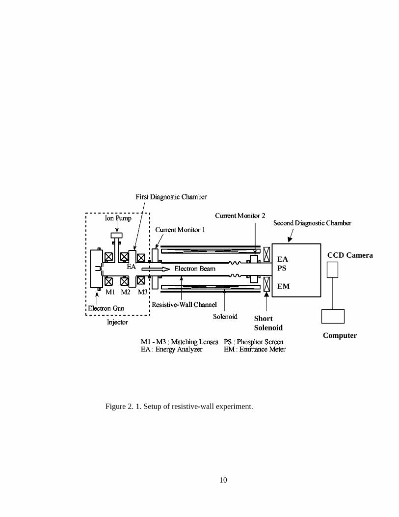
2.1 Experimental Setup
Figure 2.1 shows the experimental setup for the resistive-wall instability
experiment. The facility consists of an electron gun, three matching solenoids, a
long solenoid channel and two diagnostic chambers. The beam is emitted from the
electron gun with various beam energies. The beam pulse shape is controllable,
either rectangular or parabolic. Usually we use a rectangular profile. On the flat top
of the beam, a localized perturbation can be launched by the method which will be
described in the next section. Three matching solenoids can be adjusted so that the
beam is matched into the long solenoids. Inside the long solenoids there is a
resistive tube for the study of the resistive wall instability. There are several
diagnostic tools employed in this experiment. They are beam current monitors,
phosphor screens, a Rogowski coil and energy analyzers.
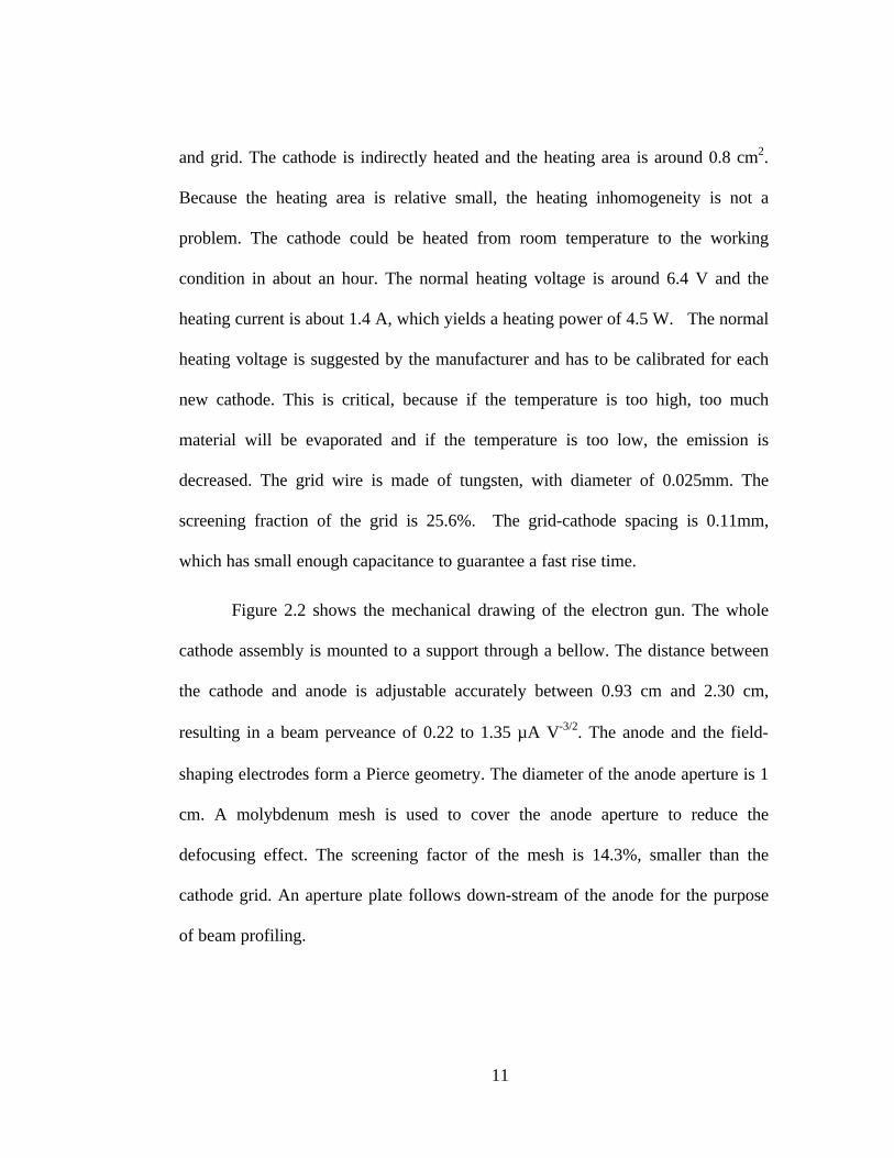
2.2 Electron Gun
The electron gun used in the experiment is a variable-perveance gridded
gun developed and constructed at the University of Maryland [13]. The electron has
a Pierce type geometry and a planar configuration consisting of the heater, cathode
10
Figure 2. 1. Setup of resistive-wall experiment.
EAPS
EM
Computer
CCD Camera
ShortSolenoid
11
and grid. The cathode is indirectly heated and the heating area is around 0.8 cm2.
Because the heating area is relative small, the heating inhomogeneity is not a
problem. The cathode could be heated from room temperature to the working
condition in about an hour. The normal heating voltage is around 6.4 V and the
heating current is about 1.4 A, which yields a heating power of 4.5 W. The normal
heating voltage is suggested by the manufacturer and has to be calibrated for each
new cathode. This is critical, because if the temperature is too high, too much
material will be evaporated and if the temperature is too low, the emission is
decreased. The grid wire is made of tungsten, with diameter of 0.025mm. The
screening fraction of the grid is 25.6%. The grid-cathode spacing is 0.11mm,
which has small enough capacitance to guarantee a fast rise time.
Figure 2.2 shows the mechanical drawing of the electron gun. The whole
cathode assembly is mounted to a support through a bellow. The distance between
the cathode and anode is adjustable accurately between 0.93 cm and 2.30 cm,
resulting in a beam perveance of 0.22 to 1.35 µA V-3/2. The anode and the field-
shaping electrodes form a Pierce geometry. The diameter of the anode aperture is 1
cm. A molybdenum mesh is used to cover the anode aperture to reduce the
defocusing effect. The screening factor of the mesh is 14.3%, smaller than the
cathode grid. An aperture plate follows down-stream of the anode for the purpose
of beam profiling.
12
Figure 2. 2. Schematics of gridded electron gun.
13
It consists of eight circular holes, one pepper-pot, one slit and two multiple-beamlet
configurations. A simple, built-in current transformer (Rogowski Coil) is located
after the aperture plate. It is very useful in the gun commissioning and emission
testing. This gun also has a gate valve to isolate the cathode from the rest of the
system. During experiments, the gate valve is open; while after experiment or
during the system installation, the gate valve is closed to protect the cathode.
Figure 2.3 shows the circuit diagram of the gun controller. The electronics
consists of a high voltage power supply for anode-grid voltage, a DC bias power
supply to supply voltage between the cathode and grid to suppress the beam, an AC
power supply to heat the cathode and finally, a grid-cathode pulse generator. All
the electronics is located in a high voltage deck, which is isolated from the ground
up to -10KV. It has a connection to the low voltage electronics via fiber optics and
insulated transformer. The cathode is usually biased by positive DC voltage relative
to the grid to cut off the beam current. During the emission, the pulse generator
produces a negative pulse between the cathode and grid to turn on the beam.
The grid-cathode pulse system is very critical to guarantee a desirable beam
waveform. It consists of a charging transmission line, a fast transformer and an
avalanche transistor. Careful attention must be taken to choose the parameters of
the transformer and the transistor to have fast rise-time pulse. The length of the

14
Figure 2. 3. Circuit diagram for electron gun.
15
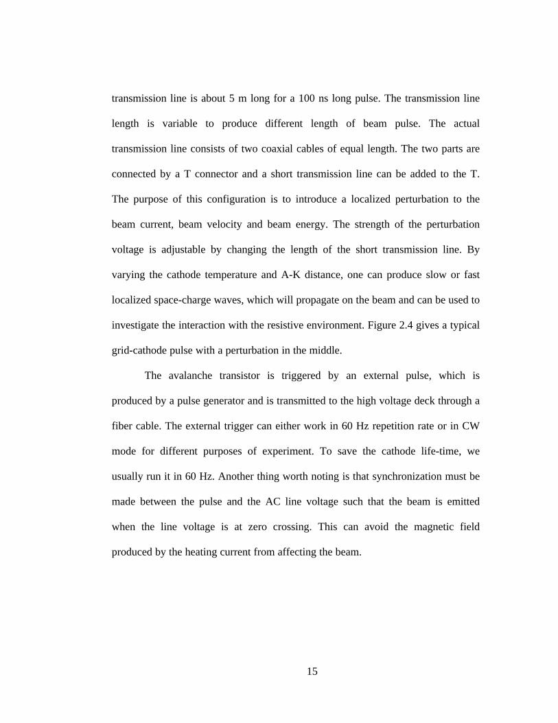
transmission line is about 5 m long for a 100 ns long pulse. The transmission line
length is variable to produce different length of beam pulse. The actual
transmission line consists of two coaxial cables of equal length. The two parts are
connected by a T connector and a short transmission line can be added to the T.
The purpose of this configuration is to introduce a localized perturbation to the
beam current, beam velocity and beam energy. The strength of the perturbation
voltage is adjustable by changing the length of the short transmission line. By
varying the cathode temperature and A-K distance, one can produce slow or fast
localized space-charge waves, which will propagate on the beam and can be used to
investigate the interaction with the resistive environment. Figure 2.4 gives a typical
grid-cathode pulse with a perturbation in the middle.
The avalanche transistor is triggered by an external pulse, which is
produced by a pulse generator and is transmitted to the high voltage deck through a
fiber cable. The external trigger can either work in 60 Hz repetition rate or in CW
mode for different purposes of experiment. To save the cathode life-time, we
usually run it in 60 Hz. Another thing worth noting is that synchronization must be
made between the pulse and the AC line voltage such that the beam is emitted
when the line voltage is at zero crossing. This can avoid the magnetic field
produced by the heating current from affecting the beam.
16
Figure 2. 4. Typical grid-cathode pulse in the electron gun. The bump in the
middle is the perturbation introduced intentionally.
-70
-60
-50
-40
-30
-20
-10
0
10
-50 0 50 100 150 200
Vol
tage
(V)
Time(ns)

17
2.3 Matching Lenses and Long Solenoid Transport
Downstream of the electron gun are there three matching lenses. The first
two solenoids have the same inner diameter of 7.6 cm and the third one has inner
diameter of 4.7 cm. Each solenoid has thickness of 6.8 cm. Three DC power
supplies are used to power each solenoid so that each of them can be adjusted
individually.
These three solenoids are characterized previously [14]. A single formula
could be used to represent these lenses. The formula is
2
20
2
)(
00 )(1
)(2
20
a
zz
eBzB
d
zz
z −+
=
−−
. (2. 1)
Here, B0 is the maximum axial magnetic field. z0 is the center position of the
solenoids. d and a are parameters to control the field profile. They are different for
each solenoid. Table 2.1 shows all the parameters for three solenoids. In the table,
M1, M2 and M3 represent the first, second and third solenoids respectively. B0 is
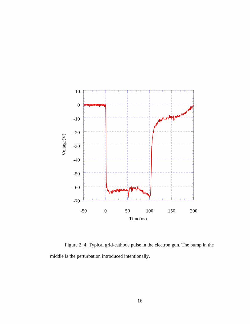
the peak magnetic field in Gauss per ampere. Figure 2.5 shows the axial magnetic
field profile of the first solenoid. In the figure, two lines indicate the physical edge
of the solenoid. The fields drop to about 40% at the physical edge and almost zero
at 11 cm.
18
Figure 2. 5. Axial magnetic field profile for the first solenoid. Two lines
indicate the physical edges of the solenoid.
0
0.2
0.4
0.6
0.8
1
-15 -10 -5 0 5 10 15
Nor
mal
ized
Axi
al M
agne
tic F
ield
Distance (cm)

19
Table 2. 1. Parameters for three matching solenoids
Solenoids B0 (Gauss/A) d (cm) a (cm)
M1 17 4.475 3.422
M2 17 4.168 3.592
M3 20 2.82 3.36
It is worth noting that the field produced by a short solenoid is not a perfect
uniform field across the beam section area. Due to the higher order field, the peak
magnetic field changes with the radius. If the zero order of the magnetic field is
given by Equation (2.1), then the total axial magnetic field including up to forth
order could be represented as
64)(
4)()(
4''''0
2''004
rzB
rzBzBB zzzz +−= . (2. 2)
Note that Bz4 is radius dependent and usually increases with the radius. Figure 2.6
shows the dependence of the peak magnetic field on the radius. In the figure, the
field is normalized by Bz0 at z=0. At r=0, the field is equal to Bz0, and it increases
by about 5% in one centimeter. This nonlinear effect will change the beam
envelope calculation slightly.
20
Figure 2. 6. Solenoid axial field vs. radius including upto 4th term.
1
1.05
1.1
1.15
0 0.2 0.4 0.6 0.8 1 1.2 1.4 1.6
Nor
mal
ized
Axi
al M
agne
tic F
ield
Radius (cm)

21
After three matching lenses is a long solenoid, which offers uniform
focusing to the beam. The solenoid is 138.7 cm long. It is made of copper windings
on an aluminum tube with diameter of 11.5 cm. There is an iron tube at the outside
of the copper windings to restrict the field lines. The axial magnetic field is uniform
inside the solenoid. However, at the edges, the fields decay with the distance. For
the purpose of simulating the beam envelope, we have to measure the field profile
at the edges. The fields are measured by a Bell gaussmeter with a longitudinal Hall
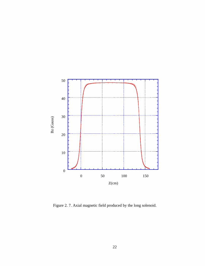
probe. Figure 2.7 shows the measured axial magnetic field profile along the axis.
The horizontal axis is the distance along the solenoid and zero position is the
physical edge of the solenoid. The circles represent measurement points. Fitting
curve is also shown in the figure. The fitted formula for the field profile is
)))(()(
()(2222/1220
alz
lz
az
zcBzBz +−
−−
+= . (2. 3)
Here, c, a and l are empirical parameters for best fitting. Their numbers are
c=0.5027, a=5.0408 cm and l=137.08 cm respectively for this long solenoid. B0
corresponds to the uniform field inside the solenoid. It depends on the beam current
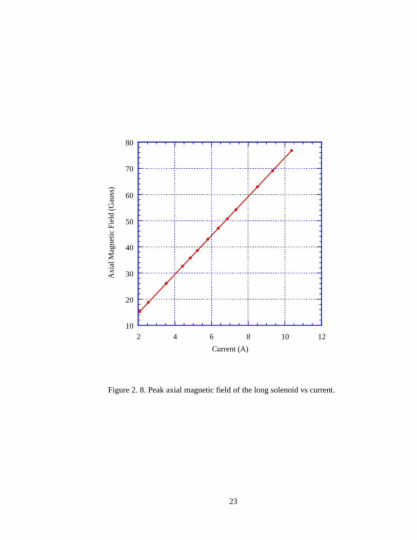
and the solenoid winding. Figure 2.8 shows the dependence of B0 on the solenoid
current. The round points are the measurement data and the line is the fitting curve.
The fitted formula for B0 is
IB ×+−= 4152.71296.00 . (2. 4)
22
Figure 2. 7. Axial magnetic field produced by the long solenoid.
0
10
20
30
40
50
0 50 100 150
Bz
(Gau
ss)
Z(cm)
23
Figure 2. 8. Peak axial magnetic field of the long solenoid vs current.
10
20
30
40
50
60
70
80
2 4 6 8 10 12
Axi
al M
agne
tic F
ield
(G
auss
)
Current (A)
24
Here the unit for B0 is Gauss and I is the solenoid current, in amperes.
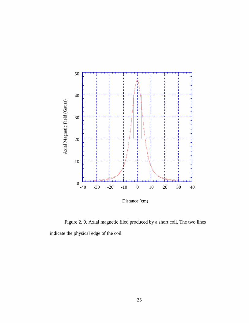
Due to the physical limitation, there is a gap between the exit of the long
solenoid and the entrance of the diagnostic chamber. To prevent the beam from
blowing up, a short coil is added to produce magnetic fields to focus the beam. For
simplicity, this coil is wound on an aluminum tube without iron around it. Fields
are smaller without the iron, but they are still large enough to focus the beam. The
physical length of the coil is 5.6 cm. Figure 2.9 is the measured magnetic field
profile along the axis. Two lines indicate the physical edges of the solenoid. Note
that due to lack of the iron, the field extends much longer than in the previous case
and the peak field is also much smaller. Curve fitting gives the formula of the field
profile as
)))
2((
2
))2
((
2()(2222/122
0
al
z
lz
al
z
lz
cBzBz
+−
−−
++
+= . (2. 5)
Here, c=1.4237, l=4.5322 cm and a=6.0416 cm. B0 is the peak axial magnetic field
and its dependence on the wire current is given by
IB ×+= 688.539107.00 . (2. 6)
Again, B0 is in the unit of Gauss, and I is the current, in amperes. Figure 2.10
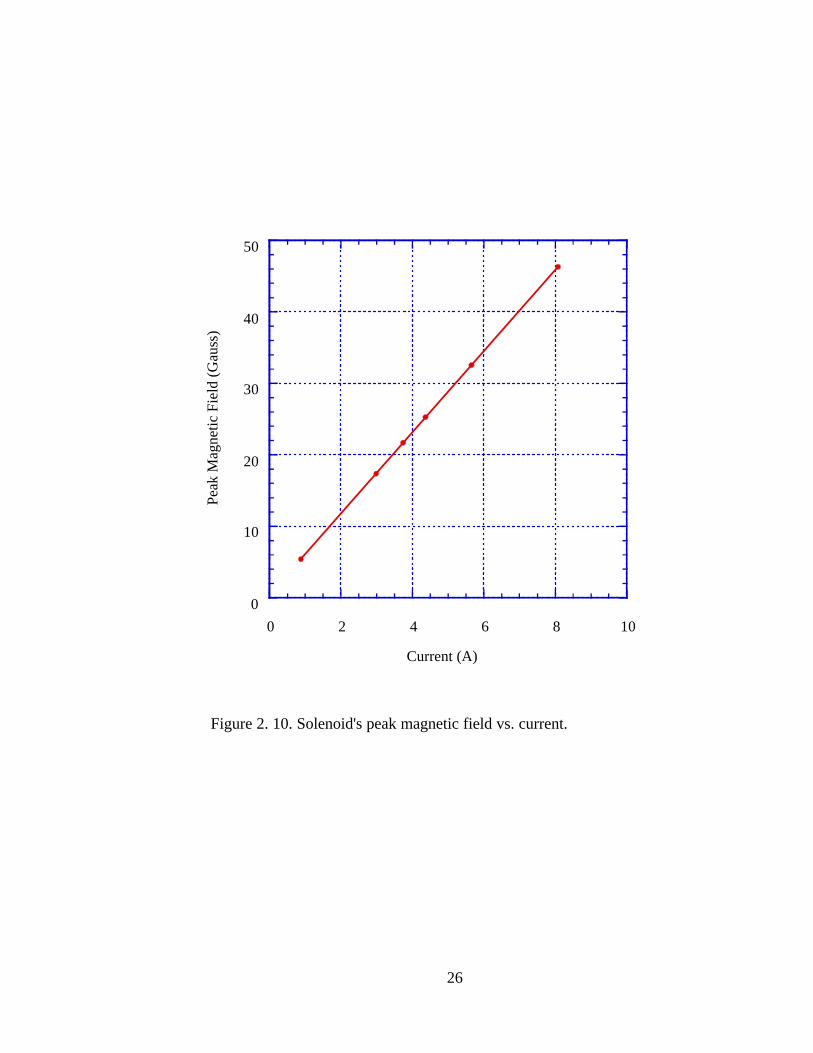
shows the measurement points for this formula.
25
Figure 2. 9. Axial magnetic filed produced by a short coil. The two lines
indicate the physical edge of the coil.
0
10
20
30
40
50
-40 -30 -20 -10 0 10 20 30 40
Axi
al M
agne
tic F
ield
(G
auss
)
Distance (cm)
26
Figure 2. 10. Solenoid's peak magnetic field vs. current.
0
10
20
30
40
50
0 2 4 6 8 10
Peak
Mag
netic
Fie
ld (
Gau
ss)
Current (A)
27
2.4 Resistive-Wall Tubes
The key component in the resistive-wall channel is a glass tube coated with
resistive material. The resistive material in the inner surface is Indium-Tin-Oxide
(ITO). Total resistance of the tube is 10.1 kΩ. The resistive part of tube is 0.99 m
long and has inner diameter of 3.8 cm, which corresponds to an area resistivity of
1.22 kΩ per square. It has bellows and metal parts with flanges at both ends to
connect to other components. Silver paste is used to make good contact between
the resistive material and the metal parts. Total length of the tube including metal
parts is 123 cm. These glass tubes were custom made for us at the Institute of
Vacuum Electronics, Beijing, China.
2.5 Diagnostics
The diagnostic tools installed in the experiment include energy analyzers,
current monitors and a phosphor screen. The main tool is the energy analyzer. The
energy analyzer was developed by Hyyong Suk, the former Ph.D. student. The
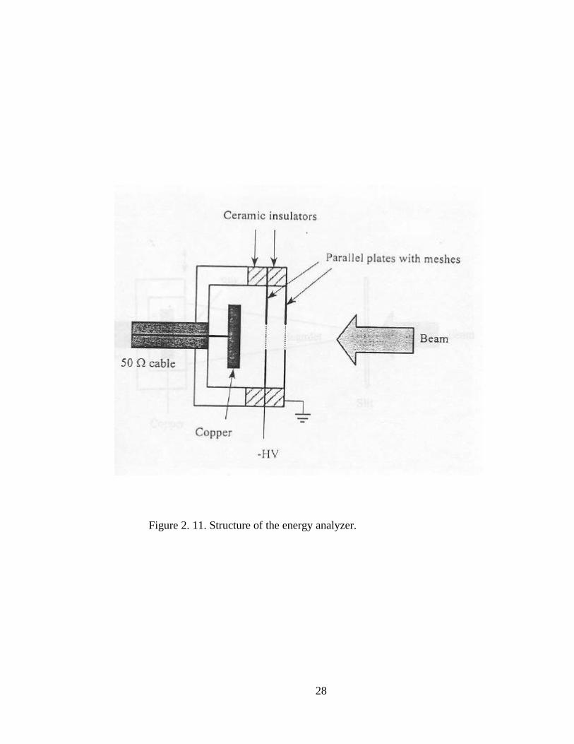
geometry of the energy analyzer is illustrated in Figure 2.11 [7]. As shown in the
figure, it consists of two parallel plates and one collector. Two plates have a hole
with diameter of 4.8 mm. The holes are covered with wire meshes to produce a
uniform electric field. The collector is connected to 50 Ω channel of a digital signal
analyzer (Tektronix DSA 602A) through vacuum feedthrough. Chapter 4 will
explain the principle of the energy analyzer in detail.
28
Figure 2. 11. Structure of the energy analyzer.
29
There are two resistive-wall type current monitors in the system. The total
resistance for each current monitor is 1.1 Ω so the sensitivity is 1.1V/A.
Another tool in the experiment is phosphor screen. With a CCD camera and
a computer, the beam image on the phosphor screen can be digitized and processed
later by a computer program.
There are two diagnostics chambers in the system. The first chamber is
located between the second and third solenoids. It contains a retarding voltage
energy analyzer. The position of the energy analyzer could be accurately adjusted
by a linear and rotation feedthrough. When we measure the energy of the beam, the
energy analyzer is laid down to the center of the pipe. When we do the
measurement downstream, the energy analyzer is lifted up to let the beam pass by.
The second diagnostic chamber is located after the resistive wall. This
chamber has a phosphor screen, a retarding voltage analyzer and a slit-slit
emittance meter in it. All of the diagnostics are adjustable and can move inside the
chamber independently.
2.6 Vacuum System
Vacuum is very important to the experiment. Due to the scattering between
the beam and the residual gas, poor vacuum will cause beam emittance growth and
other beam quality deterioration [1]. In this experiment, because the cathode is
getting old, it also requires good vacuum (10-9 Torr) to have good emission.
30
Tremendous attention was taken to obtain high vacuum. Every new component has
to be cleaned using alconox, deionized water, methanol, acetone and TCE.
The vacuum system consists of a turbo-molecular roughing pump and five
ion pumps. The ion pump speeds are 8 l/s, 60 l/s, 40 l/s and 30 l/s respectively. The
8 l/s pump is located on top of the electron gun. The 60 l/s pump is located between
the first and second solenoids. It is about two feet away from the beam line to avoid
the magnetic field from affecting the electron beam. The 40 l/s and 30 l/s pumps are
connected to the second diagnostic chamber. To pump down the vacuum, we first
use the turbo-molecular pump to pump down to 10-7 Torr range. This step will take
several hours. Then the ion pumps are turned on to bring the pressure down to 10-8
Torr. After that, heating tapes are used to bake the system to about 160o C to
remove any moisture and other residual gas. Sometimes, aluminum foils are
wrapped around the system to have higher baking temperature. However, care must
be taken not to damage the component, especially the ion pump magnet, with
which the baking temperature can not be higher than 250o C. After these steps,
usually the system pressure could be around low 10-9 Torr range. The whole
procedure will take about two weeks for each procedure starting from the air
pressure.

31
Chapter 3
Space-Charge Waves in Electron Beams Propagating Through
a Resistive-Wall Channel
3.1 Motivation
Transport and acceleration of intense charged particle beams with high
quality are important issues in advanced accelerator applications such as colliders
for high-energy physics, induction linacs for heavy-ion inertial fusion, high
intensity linacs and synchrotrons for spallation neutron sources, etc. Due to the
requirements of ever increasing beam intensity in these applications, space-charge
effects and collective behavior among charged beam particles play a crucial role in
the beam dynamics, which may limit the maximum transportable beam current and
deteriorate the beam quality. One such collective phenomenon is longitudinal
space-charge waves generated by line-charge perturbations on beams, and
longitudinal instabilities caused by the interaction between the space-charge waves
and a dissipative environment, i.e. a resistive transport channel. For example, a
heavy-ion fusion driver may consist of many induction modules. An induction
accelerator for heavy ion fusion would have currents of heavy ions in the range
between 20 to 30 KA and energy of 5 to 10 GeV. The average wall resistance of
such an induction accelerator is about 100-300Ω/m. Longitudinal space-charge
32
waves can be generated on beams due to fluctuations in the bunch, mismatch
between external focusing forces and space-charge forces, and other effects. Their
propagation on beams and interaction with this kind of resistive environment leads
to growth of slow space-charge waves due to the resistive-wall instability. The
instability is caused because a perturbation in the beam current produces a
corresponding perturbation in the return current, which flows through the wall.
Ohm’s law tells us that a current through a resistive wall requires an electric field.
This electric field, on the other hand, may enhance the perturbation in the beam
current and cause instability. The resistive-wall instability increases the
longitudinal beam energy spread and may cause a dilution of the transverse
emittance. The increase of the longitudinal beam energy spread and transverse
emittance, in turn, makes it difficult to focus the beam into a short pulse and on a
small spot. Therefore, the resistive-wall instability has become a concern for the
success of this program.
The investigation of the longitudinal instability in charged particle beams has
a long history. The early work on the instability was originated from the study of
microwave tubes [8, 15]. Since 1980, the problem of the longitudinal instability has
received new attention in connection with research on high-current accelerators for
various applications. There has been some theoretical work in this area [1, 16, 17].
But there has been no experiment dedicated to this topic except in the EBTE group
at the University of Maryland, under the direction of Prof. Reiser [18-22]. In the
33
applications of microwaves, the conventional approach is to use sinusoidal signals
to generate space-charge waves. In the experiments conducted at the University of
Maryland, localized waves are used as beam diagnostics. This has many advantages
to the sinusoidal wave in diagnosing some beam parameters such as the wave
propagation speed, the geometry factor g for the longitudinal space-charge field,
the beam radius and so on. Also, this is the usual case for the instability in the
induction linacs for heavy-ion fusion. Another feature of these experiments is that
an electron beam, instead of a heavy-ion beam, is used. Because the electron has a
much smaller mass than heavy ion, it is possible to observe the instability in a short
facility (~ 1 m) with large resistivity.
In this chapter, a brief review of the linear theory of the resistive-wall
instability is given first. Then the experimental results in both linear and non-linear
regime are reported. In the linear regime, we can observe the results predicted by
the theory. However, in the non-linear regime, some abnormal phenomena are
observed.
34
3.2 Linear Theory on the Resistive-Wall Instability
3.2.1 Resistive-Wall Instability Theory Based on One-dimensional Model
and Vlasov Equation.
The resistive-wall instability can be studied with different methods. One
usual way is to use one-dimensional cold fluid equation to study the resistive-wall
instability [23, 24]. Another way is to use one-dimensional Vlasov equation. This
method can give more general results and also can be applied to the case of beam
with energy spread or Landau-damping effect. Here, we will follow the second
approach.
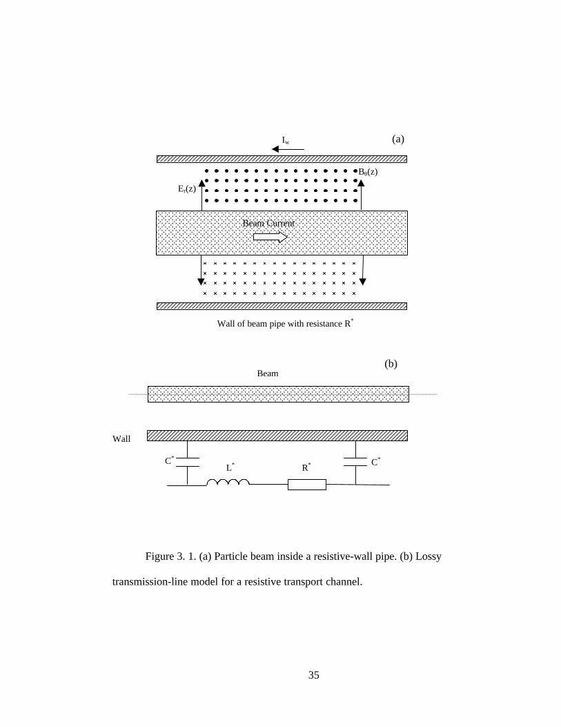
As been illustrated in Figure 3.1, suppose that a beam of momentum p is
transported in a cylindrical pipe with wall impedance Zw. Its one-dimensional
distribution function has the form
),,()(),,( 10 tpzfpftpzf += . (3. 1)
Here, the subscript 0 represents the unperturbed quantity while the subscript 1
represents the perturbed term. In the linear theory, it is always assumed that the
perturbation is small compared to the unperturbed term. The perturbed line charge
and current are subject to the continuity condition
0),(),( 11 =
∂∂
+∂
Λ∂z
tzi
t
tz. (3. 2)
35
Figure 3. 1. (a) Particle beam inside a resistive-wall pipe. (b) Lossy
transmission-line model for a resistive transport channel.
Iw
Er(z)
Bθ(z)
Beam Current
Wall of beam pipe with resistance R*
(a)
Beam
Wall
C*C*
R*L*
(b)

36
Here, Λ1(z,t) is the perturbed line charge density and i1(z,t) is the perturbed beam
current. The second equation governing the perturbation is the linearized one-
dimensional Vlasov equation
p
pftzqEtpzf
pqE
zv
t ∂∂
−=
∂∂
+∂∂
+∂∂ )(
),(),,( 0110 . (3. 3)
In the equation, E0 is the unperturbed electrical field which should be zero in the
uniform beam, and E1 is the electric field due to perturbation. It can be expressed
by
),(),(),(1 tzEtzEtzE ws += , (3. 4)
where Es(z,t) is the axial electric filed due to non-uniform line charge density and
beam current and Ew(z,t) is the electrical field due to wall impedance. By long
wavelength approximation, Es(z,t) is related to beam current and density by
)),(1),(
(4
),( 12
1
0 t
tzi
cz
tzgtzEs ∂
∂+
∂Λ∂
−=πε
, (3. 5)
where g is the geometry factor and is given by g=2ln(b/a) with a and b being the
beam radius and pipe radius respectively. c is the speed of light and ε0 is the
permittivity of vacuum. In the frequency domain, the Ew(k,ω) is related to the wall
impedance per unit length by
∫Λ−= dptpzvfkZkEw ),,(),(),( 10* ωω ω . (3. 6)

37
Here, Zω* is the wall impedance per unit length and v is the beam velocity.
If assume that the perturbation has the form of exp[i(ωt-kz)], and plug the
above equations into (3.3), we can get the dispersion equation[21]
[ ] ∫ =−
×+Λ− 0)(
),(),(1
230**
0 dpkv
pfkZkZ
miq s ωγ
ωωω
ω . (3. 7)
Here, Zs* is defined as the space-charge wave impedance per unit length and can be
expressed as
0
2*
4),( Z
c
ckgikZ s
+−=
ωωπ
ω , (3. 8)
where c is the speed of light and Z0 is the characteristic impedance of free space,
equal to 377 Ω.
So far this dispersion equation is valid for different wall impedance within
the framework of the theoretical model. In the following section, we will apply this
equation to various situations.
3.2.2 Space-Charge Waves in a Monoenergetic Electron Beam With
Conducting, Resistive and Complex Wall Impedance
First let us assume that the electron beam has no energy spread and the
distribution function is expressed by
)()( 00 pppf −= δ . (3. 9)
In this case, the dispersion equation is reduced to
38
),(),()( **20
0
3
ωωωω
γω kZkZkv
q
mi s +=−
Λ− . (3. 10)
Here, v0 is the beam velocity. Using the model in Figure 3.1, the wall impedance
can be written as
***www iXRZ += . (3. 11)
If we use the assumption that 00 kv≈ω , the space-charge impedance per unit length
can also be approximated as [1]
022**
4Z
c
giiXZ xs γβπ
ω−=−= . (3. 12)
Using Equations (3.11) and (3.12), we can solve Equation (3.10) and get the
expressions for real and imaginary part of the wave number k as
( ) ( )
−−−+
±=
2/1**2**2*
2/1
000 1 swswwr XXXXR
Zk
Kkk
βπ
(3. 13)
and
( ) ( )2/1
**2**2*
2/1
000
−−−+
= swxwwi XXXXR
Zk
Kkk
βπm , (3. 14)
39
where K is the generalized beam perveance and Z0 is the impedance of free space.
The real part kr corresponds to the travelling wave part and the imaginary part ki
corresponds to the spatial growth part of the wave.
In the conductor wall case, both Rw* and Xw
* are zero, then Equation (3.14)
shows that ki is equal to zero and kr is reduced to
±=
00 1
v
ckk s
r . (3. 15)
Here cs is the wave speed in the beam frame, defined as
2/1
500
0
4
Λ=
m
qgcs γπε
. (3. 16)
The above equation tells us that when there is a perturbation in the electron beam
with conducting wall, the perturbation will propagate inside the beam with wave
velocity cs. There are two waves, one is fast wave, which moves forward in the
beam frame and another one is slow wave, which moves backward.
Let us take an example of parameters of the beam in our experiment to
calculate cs. For a beam with energy 3.5 keV, beam current 16 mA. The above
equations give us beam velocity of 3.49×10⁷ m/s and wave velocity cs of 1.176×10⁶
m/s. The ratio of the wave velocity to the beam velocity is 3.4%, which is
consistent with our assumption.
If the beam pipe has pure uniform resistance, the wall impedance is
expressed as

40
**ww RZ = . (3. 17)
Plug this equation into equations (3.13) and (3.14), we get
++
±=
2/1*2*2*
2/1
000
1 sxwr XXRZk
K
vk
βπω, (3. 18)
and
2/1*2*2*
2/1
000
−+
= sxwi XXR
Zk
K
vk
βπωm . (3. 19)
Here, k0 is defined as ω/v0 and K is the generalized beam perveance. If we assume
that Rw*<<Xs
*, then the above equations can be reduced to
±=
00 1
v
ckk s
r , (3. 20)
and
2/1
00
*
2
=
βγπ
gI
I
Z
Rki m . (3. 21)
In the equation, I0 is the characteristic current of the electron beam, which is
defined as qmc /4 30πε . From this relationship, we find that fast waves and slow
waves still propagate with the same speed as in the conducting wall case. However,
the imaginary part of the wave vector is not zero in this case, which means that the
wave will grow or decay spatially. In the resistive-wall instability, the fast wave

41
will decay and the slow wave will grow. Notice that in the regime defined by Eqs.
(3.20), (3.21), the growth/decay rate in this condition, the growth rate of the wave
is independent of the frequency. The growth/decay rate ki depends on the resistance
per unit length of the transport channel and the beam current and the beam energy
through the factor βγ. Higher channel resistance and beam current lead to higher
growth/decay rate, higher energy decreases the growth/decay rate.
To apply the above theory to a laboratory beam, let us take the example of a
3.5 keV electron beam with I=16 mA, Rw*=10 kΩ, g≅2. From equation (3.21), we
find ki=0.33 1/m. The e-folding growth distance is around 3m. Figure 3.2 shows the
growth/decay rate at different beam energy and beam current in a pure resistive
channel.
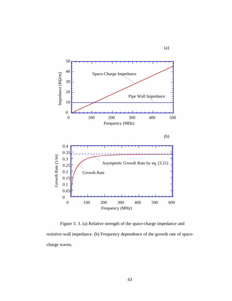
If the space-charge impedance is not larger than the wall impedance, then
we have to use equations (3.18~3.19) to calculate the growth rate. Because the
space-charge impedance depends on the frequency, the growth rate in this case is
also frequency dependant. Figure 3.3a shows the relative strength of the space-
charge impedance and the wall impedance. At low frequency, the space-charge
impedance is smaller than the wall impedance. However, it becomes larger than the
wall impedance at the frequency above 150 Mhz. Figure 3.3b shows the frequency
dependence of the growth rate. The growth rate increases with the frequency and
approaches to the number indicated by equation (3.21), shown by a horizontal line.

42
Figure 3. 2. Space-charge wave growth/decay rates at various beam energies
and beam current for 10 kΩ resistive tube.
0.2
0.4
0.6
0.8
1
1.2
1.4
1.6
0 2 4 6 8 10
Gro
wth
/Dec
ay R
ate(
/m)
Beam Energy (keV)
I=100 mA
I=40 mA
I=10 mA
43
Figure 3. 3. (a) Relative strength of the space-charge impedance and
resistive-wall impedance. (b) Frequency dependence of the growth rate of space-
charge waves.
(a)
0
10
20
30
40
50
0 100 200 300 400 500
Impe
danc
e (K
Ω/m
)
Frequency (MHz)
Space-Charge Impedance
Pipe Wall Impedance
(b)
0
0.05
0.1
0.15
0.2
0.25
0.3
0.35
0.4
0 100 200 300 400 500 600
Gro
wth
Rat
e (1
/m)
Frequency (MHz)
Growth Rate
Asymptotic Growth Rate by eq. (3.21)
44
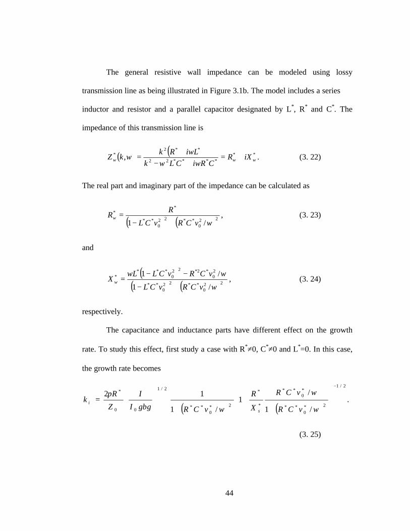
The general resistive wall impedance can be modeled using lossy
transmission line as being illustrated in Figure 3.1b. The model includes a series
inductor and resistor and a parallel capacitor designated by L*, R* and C*. The
impedance of this transmission line is
( ) ( ) ******22
**2* , www iXR
CRiCLk
LiRkkZ +=
+−+
=ωω
ωω . (3. 22)
The real part and imaginary part of the impedance can be calculated as
( ) ( )220
**220
**
**
/1 ωvCRvCL
RRw
+−= , (3. 23)
and
( )( ) ( )22
0**22
0**
20
*2*220
****
/1
/1
ω
ωω
vCRvCL
vCRvCLLX w
+−
−−= , (3. 24)
respectively.
The capacitance and inductance parts have different effect on the growth
rate. To study this effect, first study a case with R*≠0, C*≠0 and L*=0. In this case,
the growth rate becomes
( ) ( )
2/1
2*0
**
*0
**
*
*
2*0
**
2/1
00
*
/1
/1
/1
12−
++
+
=
ω
ω
ωβγ
π
vCR
vCR
X
R
vCRgI
I
Z
Rk
s
i .
(3. 25)

45
Compared to equation (3.21), we find that the growth rate is smaller due to the
capacitance of the channel.
In another case, if we assume that R*≠0, C*=0 and L*≠0, then the growth
rate can be expressed as
+
=
*
*2/1
00
*
21
2
s
i X
L
gI
I
Z
Rk
ωβγ
π. (3. 26)
As expected, in this case, the inductance of the transport channel increases the
growth rate.
3.2.3 Landau Damping
As mentioned before, Vlasov equation can also be used to the case of the
beam with initial energy spread. The beam energy spread can decrease the growth
rate or prevent the instability from developing. This effect is known as Landau
Damping in the literature [1]. Landau damping has been studied extensively in the
circular accelerators. Reference [21] has a complete theory on the linear machine
with complex wall impedance. With appropriate distribution function and the
dispersion equation, the theory can predict the boundary between the stability and
instability. It shows that, due to the initial energy spread, the stable region can be
created in the otherwise unstable region. Both Lorentz distribution and Gaussian
distribution are used in the analysis.

46
3.3 Experimental Study of the Resistive-Wall Instability
3.3.1 Generation of Space Charge Waves
An experimental facility has been set up to study the resistive-wall
instability of space-charge-dominated beam. The experiment setup is shown in
Figure 2.1, and has been described in Chapter 2.
In the experiment, localized perturbation is used to study the interaction of
electron beams with the beam pipe. The diagnostics with localized space-charge
wave is relatively easy and intuitive. It is easier to identify the fast wave and slow
wave and their propagation through the channel. To generate the space-charge
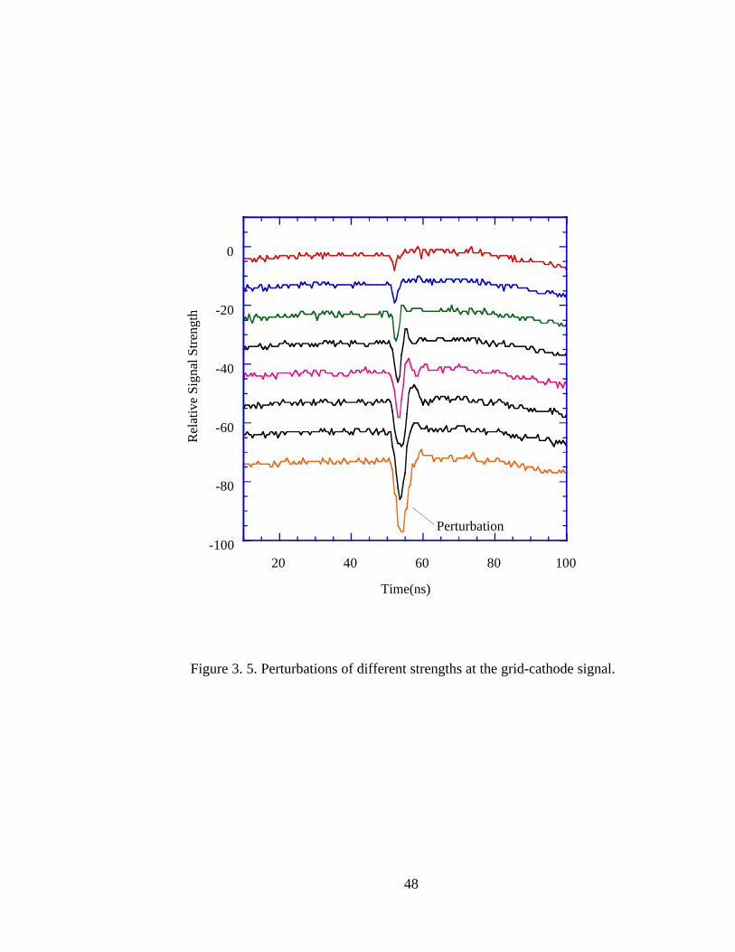
waves, we modulated the cathode-grid pulse with a small bump as shown in Figure
3.4. The strength of the perturbation can be adjusted by using different lengths of
cables as described in Chapter 2. Figure 3.5 shows the perturbations with different
strength produced by different cables. For clarity, only the perturbation part is
shown in the figure.
In the sinusoidal wave case, usually both fast and slow space-charge waves
are generated when the electron beam is perturbed. However, for the localized
wave, it is possible to generate only one fast wave or slow wave, or both [27].
When both waves are generated, fast wave will move forward and slow wave will
move backward in the beam frame. If the transport channel is long enough and they

47
-1
-0.8
-0.6
-0.4
-0.2
0
-20 0 20 40 60 80 100 120 140
Vol
tage
(V
)
Time(ns)
Figure 3. 4. Cathode-grid signal with a small localized perturbation in the
middle.
48
Figure 3. 5. Perturbations of different strengths at the grid-cathode signal.
-100
-80
-60
-40
-20
0
20 40 60 80 100
Rel
ativ
e Si
gnal
Str
engt
h
Time(ns)
Perturbation
49
reach the end, they will be reflected back [28]. In our experiment, in order to study
the different behaviors of the waves, we try to avoid the mixture of both waves.
Electron gun condition can be adjusted for the purpose of generating single fast or
slow wave. The reason is as follows. The initial cathode-grid perturbation
corresponds to a positive velocity perturbation on the beam particles, which, in
turn, produces the initial density or current perturbation. The relative strength of the
initial current, or density perturbation can be varied depending on the gun
condition. For instance, an initial velocity perturbation will produce large current
perturbation if the gun is operated in the temperature-limited regime; on the other
hand, a relative small current perturbation will be produced by the same initial
velocity perturbation if the gun is in the space-charge limited regime. The relative
strength of velocity, current and density perturbation will determine whether a fast,
slow or both waves are generated. If assume that the initial velocity perturbation is
δ and the initial current perturbation is η, by the theory of reference [27], the larger
is η/δ, the stronger is the fast wave. And in some ranges, one wave becomes
dominant over another. If we want to generate a single fast wave, we operate the
gun at relative higher energy and less space-charge-limited flow. On the other hand,
to generate the slow wave, we have to reduce the beam energy and let the beam be
more space-charge-limited flow.
In the experiment, we have to be able to test whether a fast or slow wave
has been generated. Because the fast wave moves forward, and slow wave moves
50
backward, it is possible to determine it by timing the wave position. For example,
for a 3.5 keV beam with beam current 16 mA, the beam velocity is 3.49×10⁷ m/s
and the wave velocity cs is 1.176×10⁶ m/s. After the beam is transported by one
meter, the wave will propagate about 1 ns relative to the beam. This is noticeable
from the wave signal and is used in the experiment to detect the slow or fast wave.
However, because the beam expands due to space-charge force, sometimes it is
difficult to determine the exact beam position. Hence, a second method is also
used. According to the results from solving the fluid equation [27], two waves have
opposite polarity for the current waveform. In our case, the fast wave has positive
amplitude (current larger than the average beam current) and the slow wave has
negative amplitude (current smaller than the average beam current). Figure 3.6
shows the typical waveform from the current monitor for both fast and slow waves.
From the polarity of the current perturbation, we are able to tell whether a slow
wave or fast wave has been generated.
3.3.2 Beam Matching into the Resistive-Wall Channel
As discussed in Chapter 2, the magnetic system consists of three matching
lenses, one long solenoid and an extra short coil. The beam is uniformly focused in
the long solenoid; the beam envelope can be adjusted by changing the focusing
strength. The magnetic field of the long solenoids can be varied from 40 G to 80 G
for good matching. The focusing strength of three matching lenses can be
51
Figure 3. 6. (a) Fast wave signal has larger current than the main beam. (b)
Slow wave signal has smaller current than the main beam.
0.3
0.4
0.5
0.6
0.7
0.8
0.9
1
1.1
-20 0 20 40 60 80 100 120 140
Bea
m C
urre
nt (
Nor
mal
ized
)
Time(ns)
Fast wave
(a)
0.4
0.5
0.6
0.7
0.8
0.9
1
1.1
-20 0 20 40 60 80 100 120 140
Bea
m C
urre
nt (
Nor
mal
ized
)
Time(ns)
Slow wave
(b)
52
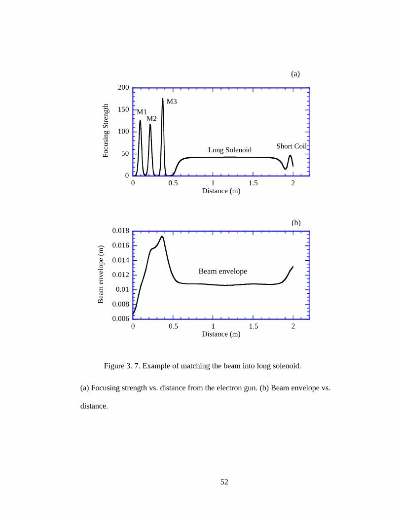
Figure 3. 7. Example of matching the beam into long solenoid.
(a) Focusing strength vs. distance from the electron gun. (b) Beam envelope vs.
distance.
0
50
100
150
200
0 0.5 1 1.5 2
Focu
sing
Str
engt
h
Distance (m)
M1M2
M3
Long Solenoid Short Coil
(a)
0.006
0.008
0.01
0.012
0.014
0.016
0.018
0 0.5 1 1.5 2
Bea
m e
nvel
ope
(m)
Distance (m)
(b)
Beam envelope

53
adjusted accordingly for the beam to be matched into the long solenoid. The peak
magnetic fields of three matching lenses range from 40 G to 100 G respectively.
A K-V envelope equation has been solved to give us an idea how the beam is
matched into the system. Figure 3.7 is one example of the matching case. Figure
3.7a gives the focusing strength of the magnetic lens. The driving currents for three
matching lens are 2.24, 2.16 and 2.25 A respectively. The long solenoid current is
3 A and the short coil current is 4 A. Figure 3.7b gives the beam envelope vs.
distance from the electron gun. A 2.5 keV and 40 mA beam is used in the
simulation. In the graph, the beam is matched into the long solenoid with little
ripple. The simulation results provide the guidelines for the experiment.
3.3.3 Experiments of Space-Charge Waves in the Linear Regime
After a space-charge wave has been generated and injected into the resistive
wall. The space-charge wave will interact with the resistive wall and will either
grow or decay. In our experiment, we study the growth or decay rate of the energy
width of space-charge wave. The energy width of space-charge waves are measured
and compared at both ends of the resistive-wall channel. This is done as follows:
by increasing the retarding voltage in the energy analyzers, the beams and space-
charge waves can be gradually suppressed in the analyzer output. First, the main
beam is suppressed at retarding voltage corresponding to the beam energy. Then,
we increase the voltage further till the wave signal is also suppressed. The
54
difference of the two voltages gives the energy width of the space-charge wave,
which is the most interesting parameter in the experiment.
Measurements with two energy analyzers for a fast wave have been
performed for a beam of energy 3.595 keV and current 19.8 mA. A typical
measurement with the first energy analyzers is shown in Figure 3.8. The location
of the first energy analyzer is at the entrance of the resistive-wall channel. The
beam is suppressed at a retarding high voltage of 3.595 kV. The remaining signal
on the top trace is a fast wave in which particles have a higher energy than the
average beam energy. When the retarding high voltage further increases, the space-
charge-wave signal decreases and eventually disappears. Figure 3.9 gives the
energy profile of the space-charge wave. This results in an energy width of 21 eV
for the fast wave. The same measurement is also done at the second energy
analyzer, which is located at the exit of the resistive-wall channel. Figure 3.10
shows the space-charge wave at different retarding voltages; and Figure 3.11 shows
the energy profile of the wave. Both figures give the energy width of the fast wave
at the second energy analyzer of 13 eV. The experiment shows that the energy
width of fast space-charge wave decreases in the resistive environment. The energy
width decreases from 21 eV to 13 eV, giving a spatial decay rate of –0.48/m.
The measurements are also done at different beam energy and beam
current. Table 3.1 shows the results from beam energy 2.5 keV, 3.5 keV and 4 keV.
The error bar for each measurement is also shown in the table. The experimental
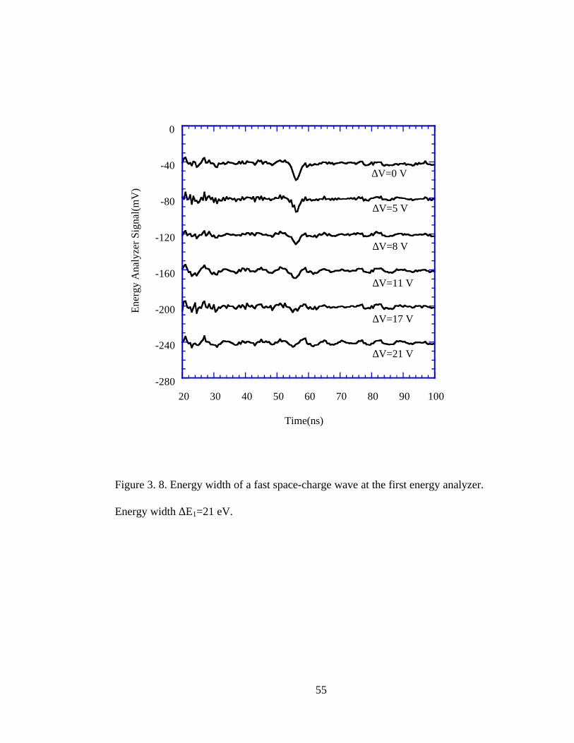
55
Figure 3. 8. Energy width of a fast space-charge wave at the first energy analyzer.
Energy width ∆E1=21 eV.
-280
-240
-200
-160
-120
-80
-40
0
20 30 40 50 60 70 80 90 100
Ene
rgy
Ana
lyze
r Si
gnal
(mV
)
Time(ns)
∆V=0 V
∆V=5 V
∆V=8 V
∆V=11 V
∆V=17 V
∆V=21 V

56
Figure 3. 9. Energy profile for a fast wave at the first energy analyzer.
0
0.2
0.4
0.6
0.8
1
1.2
0 5 10 15 20 25
Wave Energy Relative to Beam (eV)
Rel
ativ
e N
umbe
r of
Par
ticle
s in
the
Wav
e

57
Figure 3. 10. Energy width of a fast space-charge wave at the second energy
analyzer. Energy width ∆E2=13eV.
-70
-60
-50
-40
-30
-20
-10
0
80 90 100 110 120 130 140
E
nerg
y A
naly
zer
Sign
al(m
V)
Time(ns)
∆V=0 V
∆V=3 V
∆V=7 V
∆V=9 V
∆V=11 V
∆V=13 V

58
Figure 3. 11. Energy profile for a fast wave at the second energy analyzer.
0
0.2
0.4
0.6
0.8
1
1.2
-2 0 2 4 6 8 10 12 14
Rel
ativ
e W
ave
Am
plitu
de
Wave Energy Relative to Beam(eV)

59
results are compared with the calculated numbers from Equation (3.21). The
comparison shows that they agree with each other reasonably well.
Table 3. 1. Fast space-charge wave decay rate at different beam parameters
Beam Energy (keV) 2.5 3.5 4
Beam Current (mA) 15.6 19.8 23.2
∆E1 (eV) 12 ± 1 21 ± 1 18 ± 1
∆E2 (eV) 7 ± 1 13 ± 1 16 ± 1
Experimental ki (1/m) -0.54 ± 0.2 -0.48 ± 0.12 -0.12 ± 0.12
Calculated ki from
Eq.(3.21) (1/m) -0.41 -0.4 -0.39
Experiments are also performed to study the growth rate of slow space-
charge wave in the resistive-wall pipe. In the experiment, the beam energy is 2.5
keV and the beam current is 30 mA. Figure 3.12(a) is for the measurement at the
first energy analyzer while Figure 3.12(b) is for the measurement at the second
energy analyzer. This figure indicates that energy width of slow wave in the
resistive-wall channel increases from 27 eV to 37 eV, giving a growth rate of 0.32
1/m.
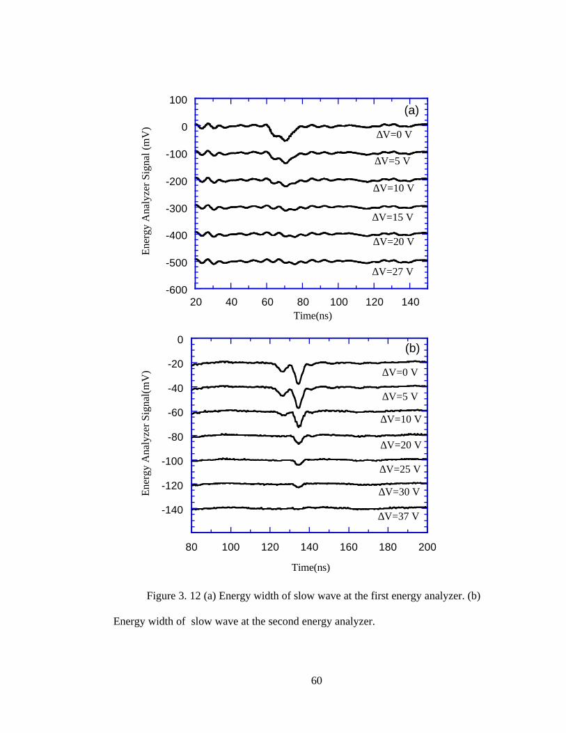
60
Figure 3. 12 (a) Energy width of slow wave at the first energy analyzer. (b)
Energy width of slow wave at the second energy analyzer.
-600
-500
-400
-300
-200
-100
0
100
20 40 60 80 100 120 140
Ene
rgy
Ana
lyze
r Si
gnal
(m
V)
Time(ns)
∆V=0 V
(a)
∆V=5 V
∆V=10 V
∆V=15 V
∆V=20 V
∆V=27 V
-140
-120
-100
-80
-60
-40
-20
0
80 100 120 140 160 180 200
Ene
rgy
Ana
lyze
r Si
gnal
(mV
)
Time(ns)
(b)
∆V=0 V
∆V=5 V
∆V=10 V
∆V=20 V
∆V=25 V
∆V=30 V
∆V=37 V
61
3.3.4 Experiments with Fast Waves in the Nonlinear Regime [43]
Measurements with the energy analyzers are also performed in the nonlinear
regime where a rather large current perturbation is introduced on the beam. This is
done by applying a strong voltage perturbation on the grid-cathode pulse of the
electron gun, which results in large line-charge density and current perturbation on
the beam. Figure 3.13 shows such a case, where the beam current signal is
modulated with a large localized space-charge wave, measured before the resistive
wall. The ratio of the wave amplitude over the average beam current is nearly
35%, a highly nonlinear case. In this experiment, we measure the evolution of the
energy width of the nonlinear fast wave against this initial perturbation strength
defined as the ratio Ip/Ib, where Ip and Ib are indicated in Fig. 3.13.
Measurements with two energy analyzers for the nonlinear fast waves have
been performed for a beam of energy 2.5 keV and current 16 mA. The result of the
measurement with the first energy analyzer is shown in Figs 3.14 and 3.15. As in
the linear regime experiment, the location of the first energy analyzer (EA1) is near
the entrance of the resistive-wall channel. The five curves in Fig. 3.14 show that the
wave perturbation signal disappears at ∆V = 20 V, where ∆V refers to the retarding
voltage above the energy-equivalent beam voltage. From this result, we infer an
energy width of 20 eV for the fast wave near the entrance of the resistive-wall
channel. The same measurement is also done at the second energy analyzer, which

62
Figure 3. 13. Beam current signal with a highly nonlinear space-charge
wave. Perturbation strength=Ip/Ib.
-0.2
0
0.2
0.4
0.6
0.8
1
-20 0 20 40 60 80 100 120 140
Bea
m C
urre
nt(n
orm
aliz
ed)
Time(ns)
perturbation
Ip
Ib
63
is located near the exit of the resistive-wall channel. In Fig. 3.15, we show the
signal profiles of the fast wave measured at the second energy analyzer (EA2),
which indicates that the energy width of the fast wave is equal to 25 eV. This result
shows that, for the nonlinear initial perturbation generated on the beam pulse, the
energy width of the fast space-charge wave increases when the beam propagates
through the resistive wall. In this particular case, the energy width of the fast wave
increases from 20 eV to 25 eV, yielding an exponential growth rate of ki =
[ln(∆V2/∆V1)]/∆z = 0.23/m, where ∆z is the length of the resistive channel.
The experimental results with the nonlinear fast waves are unexpected and
to the best of our knowledge, no theory exists that can explain them. To study the
dependence of the decay/growth rate of the fast waves on the initial perturbation
strength, systematic measurements were performed for a 2.5 keV beam with 16 mA
beam current. The waves are generated in the beam with different initial
perturbation strengths. The results are shown in Fig. 3.16, where the growth/decay
rates of the fast wave are plotted against the initial perturbation strength. In the
linear regime, the fast wave decays, as expected. When the perturbation is strong
enough, a transition from decay to growth takes place. The growth rate eventually
levels off for the strongest perturbations in the experiments.
In order to eliminate possible errors in the diagnostics, we performed the
same experiment in a conducting-wall tube, which replaced the resistive-wall tube
while all the other conditions remain the same. In this case, essentially no growth

64
or decay was observed for the fast wave within the experimental error bars, as
expected. The magnitude of the errors depends mainly on the resolution of the
energy-width measurements. The results are plotted in Fig. 3.17.
We are so far not able to interpret this unexpected phenomenon. As
mentioned earlier, no nonlinear model could be found, which would apply to our
experiment. Furthermore, to our knowledge, at the present time, no particle-in-cell
code exists that could be used to simulate our experiments. The closest simulation
studies were done with a suitably modified WARP code by D. A. Callahan et al, for
the linear case with an idealized geometry [26]. The extension of this code to the
nonlinear regime in the same ideal geometry would require substantial code
modifications and benchmarking, which would be very time-consuming and could
not be done in the very near future. The simulation of our actual experiment will
also require major code developments, which must include the launching of the
perturbations from the gridded cathode and the transition from the conducting to
the resistive-wall environment, an effort that will take several years. We plan to
pursue such work in the future.

65
Figure 3. 14. Energy width of a fast wave at the first energy analyzer. Energy width
∆E1=20 eV.
-50
-40
-30
-20
-10
0
10
20 30 40 50 60 70 80 90 100
Rel
ativ
e Si
gnal
Str
engt
h at
Dif
fere
nt V
olta
ges
Time (ns)
∆V=0 V
∆V=2V
∆V=12 V
∆V=7 V
∆V=20 V
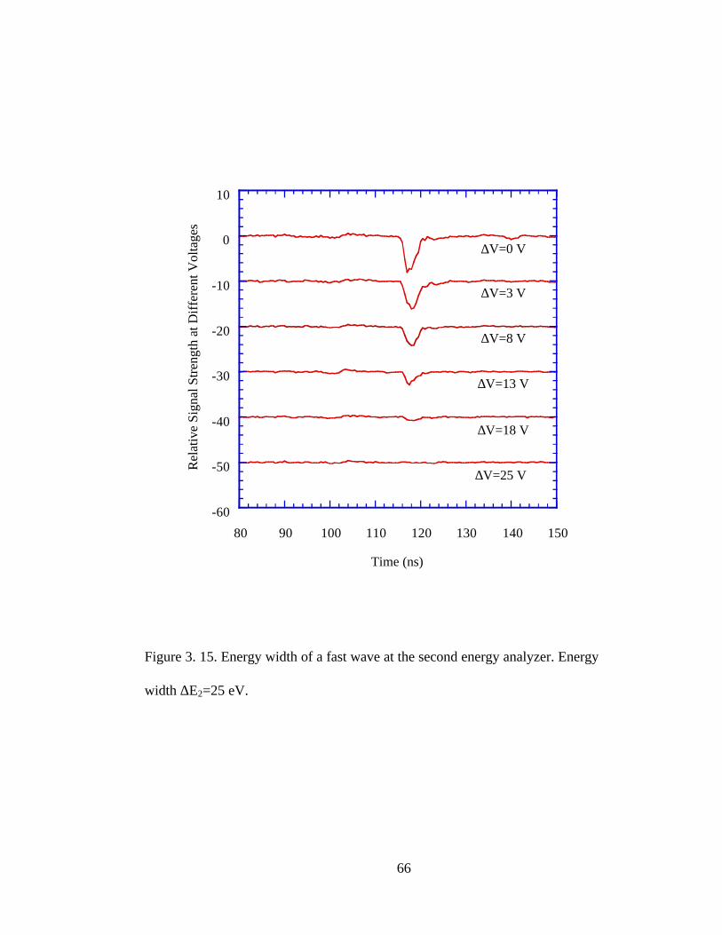
66
Figure 3. 15. Energy width of a fast wave at the second energy analyzer. Energy
width ∆E2=25 eV.
-60
-50
-40
-30
-20
-10
0
10
80 90 100 110 120 130 140 150
Time (ns)
∆V=0 V
∆V=3 V
∆V=13 V
∆V=8 V
∆V=18 V
∆V=25 V
Rel
ativ
e Si
gnal
Str
engt
h at
Dif
fere
nt V
olta
ges
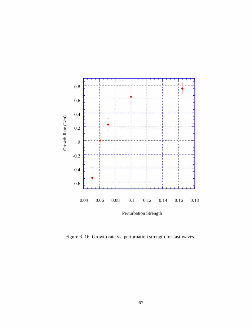
67
Figure 3. 16. Growth rate vs. perturbation strength for fast waves.
-0.6
-0.4
-0.2
0
0.2
0.4
0.6
0.8
0.04 0.06 0.08 0.1 0.12 0.14 0.16 0.18
Gro
wth
Rat
e (1
/m)
Perturbation Strength
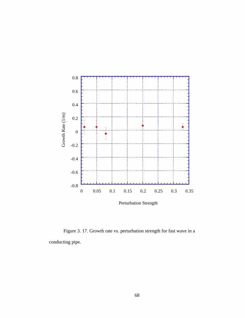
68
Figure 3. 17. Growth rate vs. perturbation strength for fast wave in a
conducting pipe.
-0.8
-0.6
-0.4
-0.2
0
0.2
0.4
0.6
0.8
0 0.05 0.1 0.15 0.2 0.25 0.3 0.35
Gro
wth
Rat
e (1
/m)
Perturbation Strength

69
3.4 Summary
Experiments have been performed to study the resistive-wall instability in a
space-charge-dominated beam. High-perveance electron beams with localized
perturbations were launched from a gridded electron gun and transported through a
short resistive-wall channel consisting of a resistive-film coated glass tube inside a
long solenoid providing uniform focusing. The energy width of the space-charge
waves developed from the perturbations was measured at both ends of the channel.
The experiments have shown that, for the small initial perturbation the energy
width of fast waves decreases, while the energy width of the slow waves increases.
However, in the nonlinear regime (large initial perturbation), we found the energy
width of fast space-charge wave grows. This apparently nonlinear effect was
unexpected, and, to the best of our knowledge, no theory exists that would predict
this phenomenon.

70
Chapter 4
Development of a High-Performance Retarding Field Energy
Analyzer
4.1 Introduction
As was discussed in the introduction, in the advanced particle accelerators
for many applications, the accelerated beams must have very low emittance and
energy spread. While there have been many experimental and theoretical
investigations of emittance growth, very little work exists on the sources and
evolution of energy spread in such beams. At the University of Maryland, various
experiments are being carried out to study space-charge-dominated electron beams.
Some of these experiments, such as the resistive-wall instability experiment and the
University of Maryland Electron Ring (UMER) [30] currently being constructed
require detailed knowledge of the beam's energy spread. The initial energy spread
of the beams from the thermionic gun and the growth of this energy spread in the
beam transport line must be measured with good accuracy. For these applications, a
high-resolution energy analyzer is a necessary. Due to its simplicity and high
signal-to-noise ratio output, the retarding field energy analyzer becomes a natural
choice for the low energy electron beam. However, in this kind of device, such as a
parallel plate structure, space-charge forces, beam trajectories, mechanical

71
misalignment, beam mismatching, etc, often lead to poor resolution of the energy
measurement. In this dissertation, we report on the design and test results of a
cylindrical retarding field energy analyzer which greatly improved the resolution
compared to a parallel-plate energy analyzer used previously in our experiments [7,
31].
4.2 Theory of Retarding Field Energy Analyzer
To characterize the energy spread of a low energy beam, two kinds of
energy analyzer are usually used. They are dispersion type and retarding field type.
Due to its simplicity and high transmission rate, retarding field energy analyzer has
been widely used. A typical application that uses a retarding field energy analyzer
is ion microfabrication, where low energy, low current and high intensity ion is
used. In the accelerator area, however, the retarding field energy analyzer is seldom
used because the beam energy is usually much higher (from MeV to GeV). In
UMER, we want to study the space-charge effect of intense beam and intentionally
use a low energy beam (10 keV). Hence retarding field energy analyzer becomes a
natural choice to characterize such kind of beam.
The simplest retarding field energy analyzer is the parallel plate energy
analyzer. Figure 4.1a shows the most primitive form of the parallel plate energy
analyzer. First, let us assume that the beam is ideal, that is, all the particle
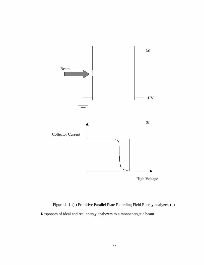
72
Figure 4. 1. (a) Primitive Parallel Plate Retarding Field Energy analyzer. (b)
Responses of ideal and real energy analyzers to a monoenergetic beam.
Beam
-HV
(a)
Collector Current
High Voltage
(b)

73
trajectories are parallel to the beam axis. After the beam enters into the energy
analyzer, the kinetic energy is converted into potential energy. Only those particles
that have higher energy than the retarding voltage can reach the collector plate and
appear as a current. Hence, if the beam is monoenergetic, the ideal response of the
energy analyzer should have a sharp cut-off at the beam energy, as shown in the
Figure 4.1(b).
In reality, the beam is never perfect. The real beam size is not infinitesimal
small, nor has it zero divergence angle. In the case of parallel plate energy analyzer,
the finite beam size is not a problem, but the finite divergence angle will cause
problem. Suppose the beam divergence angle is θ, then the axial energy is related
to the total beam energy by
2)(cos|| θt
EE = . (4. 1)
Because only the axial part of the kinetic energy is useful to overcome the
retarding potential, the starting cut off voltage would be below the beam energy by
θ2|| sinEEEE t =−=∆ (4. 2)
This formula shows that the parallel plate retarding field energy analyzer
has a fundamental resolution due to the divergence angle of the beam. Of course
this resolution depends on the quality of the beam, the smaller divergence angle of
the beam, the better resolution the energy analyzer has.

74
Besides the limitation due to the beam trajectories, the energy analyzer also
suffers from other limitations of the resolution. If we look at the structure of Figure
4.1(a), there is an aperture on the first plate for the beam to go through. This forms
an aperture lens [1], which will cause defocusing effect to the beam.
As shown in Figure 4.2, a common aperture lens has two electrical field
ranges separated by three electrodes. The center electrode is set at voltage V, the
first one is V1, and the third one is set at V2. The central plate has an aperture of
radius a, through which electrons can pass. The electrical fields at two sides of the
central plates are E1 and E2 respectively which, in general, are different. Using
classical electron optics theory, it can be proved that this aperture, along with the
different electrical field on the two sides of it, has a focal strength of [1]
1
42 1
f
E E
V=
−. (4. 3)
Here, V is the central plate voltage and f is the focal length of the aperture lens.
Applying this formula to the case of the parallel plate energy analyzer, the formula
for the focal strength is reduced to
df 4
11−= . (4. 4)
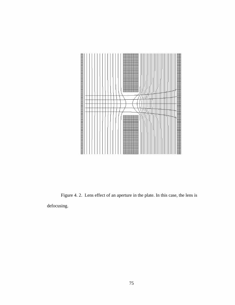
75
Figure 4. 2. Lens effect of an aperture in the plate. In this case, the lens is
defocusing.
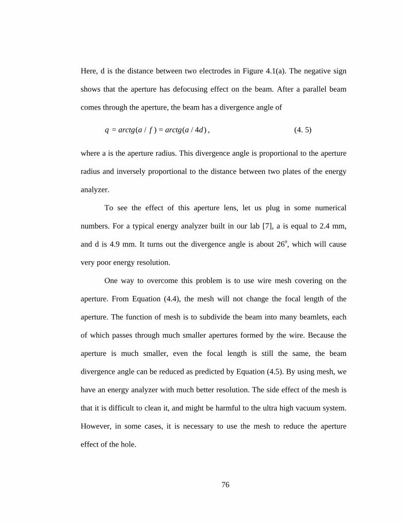
76
Here, d is the distance between two electrodes in Figure 4.1(a). The negative sign
shows that the aperture has defocusing effect on the beam. After a parallel beam
comes through the aperture, the beam has a divergence angle of
θ = =arctg a f arctg a d( / ) ( / )4 , (4. 5)
where a is the aperture radius. This divergence angle is proportional to the aperture
radius and inversely proportional to the distance between two plates of the energy
analyzer.
To see the effect of this aperture lens, let us plug in some numerical
numbers. For a typical energy analyzer built in our lab [7], a is equal to 2.4 mm,
and d is 4.9 mm. It turns out the divergence angle is about 26o, which will cause
very poor energy resolution.
One way to overcome this problem is to use wire mesh covering on the
aperture. From Equation (4.4), the mesh will not change the focal length of the
aperture. The function of mesh is to subdivide the beam into many beamlets, each
of which passes through much smaller apertures formed by the wire. Because the
aperture is much smaller, even the focal length is still the same, the beam
divergence angle can be reduced as predicted by Equation (4.5). By using mesh, we
have an energy analyzer with much better resolution. The side effect of the mesh is
that it is difficult to clean it, and might be harmful to the ultra high vacuum system.
However, in some cases, it is necessary to use the mesh to reduce the aperture
effect of the hole.
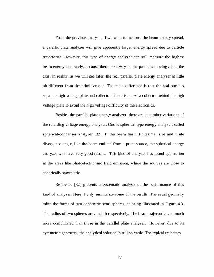
77
From the previous analysis, if we want to measure the beam energy spread,
a parallel plate analyzer will give apparently larger energy spread due to particle
trajectories. However, this type of energy analyzer can still measure the highest
beam energy accurately, because there are always some particles moving along the
axis. In reality, as we will see later, the real parallel plate energy analyzer is little
bit different from the primitive one. The main difference is that the real one has
separate high voltage plate and collector. There is an extra collector behind the high
voltage plate to avoid the high voltage difficulty of the electronics.
Besides the parallel plate energy analyzer, there are also other variations of
the retarding voltage energy analyzer. One is spherical type energy analyzer, called
spherical-condenser analyzer [32]. If the beam has infinitesimal size and finite
divergence angle, like the beam emitted from a point source, the spherical energy
analyzer will have very good results. This kind of analyzer has found application
in the areas like photoelectric and field emission, where the sources are close to
spherically symmetric.
Reference [32] presents a systematic analysis of the performance of this
kind of analyzer. Here, I only summarize some of the results. The usual geometry
takes the forms of two concentric semi-spheres, as being illustrated in Figure 4.3.
The radius of two spheres are a and b respectively. The beam trajectories are much
more complicated than those in the parallel plate analyzer. However, due to its
symmetric geometry, the analytical solution is still solvable. The typical trajectory
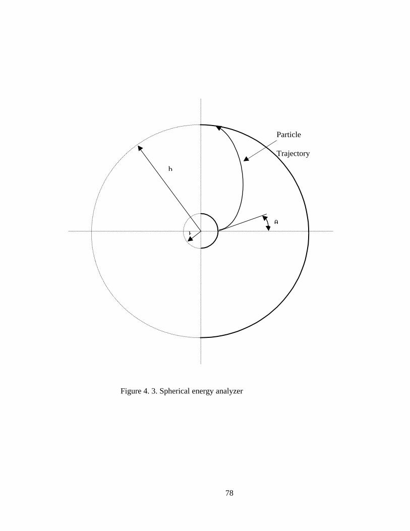
78
Figure 4. 3. Spherical energy analyzer
θ
b
b
Particle
Trajectory

79
path is an ellipse. If the particle incident angle is too large, the particle can not be
collected by the outside sphere. The largest angle that the particle could have is
determined by the following equation
)2/(sin 2 ηεθ =m . (4. 6)
Here bab /)( −=η and )2
1/( 2
0mveV=ε . This results the resolution of the energy
analyzer as
mabEE θ21 sin2/ −=∆ . (4. 7)
Unlike a parallel plate energy analyzer, even for the parallel beam of radius r0, the
energy analyzer has a finite resolution
ab
rEE
202
/ =∆ . (4. 8)
From Equations (4.2) and (4.8), we found that the parallel-plate energy analyzer
has better resolution for parallel beam while the spherical type has better
performance for point source beam.
The cylindrical energy analyzer is a compromise between the parallel plate
energy analyzer and spherical energy analyzer. As illustrated in Figure 4.4, the
second electrode of the cylindrical energy analyzer is a cylinder. This is a special
case of a normal bipotential lens and can focus the beams strongly according to the
analysis in reference [1]. The cylindrical energy analyzer has relatively

80
Figure 4. 4. Cylindrical retarding voltage energy analyzer
Beam
First Electrode V1
High Voltage Plate, V2<V1
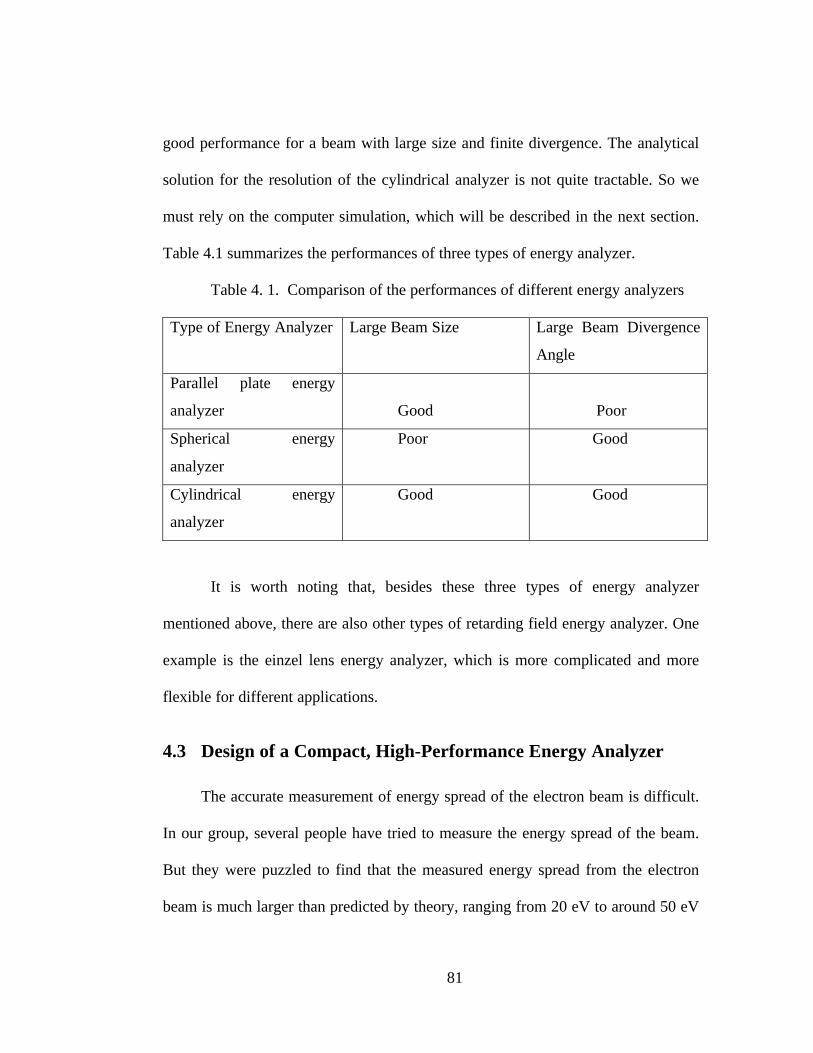
81
good performance for a beam with large size and finite divergence. The analytical
solution for the resolution of the cylindrical analyzer is not quite tractable. So we
must rely on the computer simulation, which will be described in the next section.
Table 4.1 summarizes the performances of three types of energy analyzer.
Table 4. 1. Comparison of the performances of different energy analyzers
Type of Energy Analyzer Large Beam Size Large Beam Divergence
Angle
Parallel plate energy
analyzer Good Poor
Spherical energy
analyzer
Poor Good
Cylindrical energy
analyzer
Good Good
It is worth noting that, besides these three types of energy analyzer
mentioned above, there are also other types of retarding field energy analyzer. One
example is the einzel lens energy analyzer, which is more complicated and more
flexible for different applications.
4.3 Design of a Compact, High-Performance Energy Analyzer
The accurate measurement of energy spread of the electron beam is difficult.
In our group, several people have tried to measure the energy spread of the beam.
But they were puzzled to find that the measured energy spread from the electron
beam is much larger than predicted by theory, ranging from 20 eV to around 50 eV
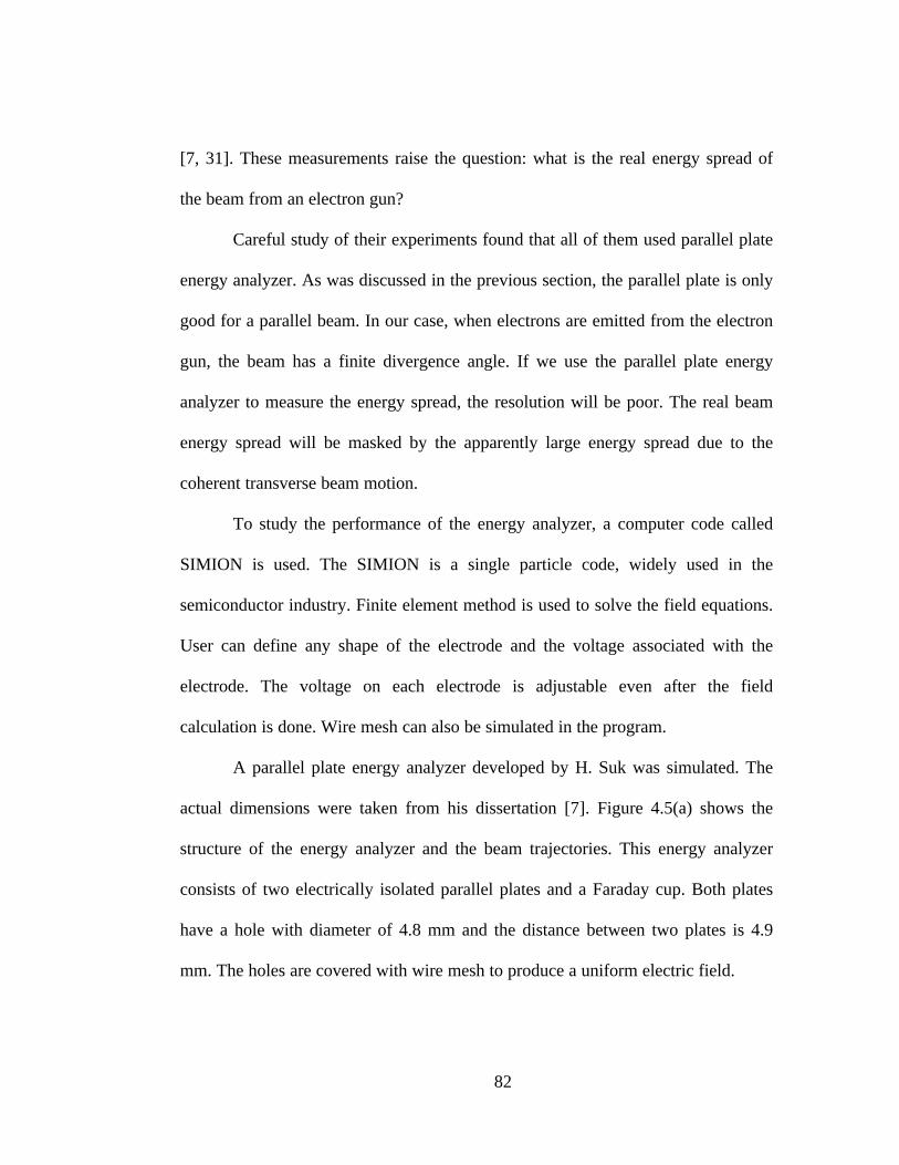
82
[7, 31]. These measurements raise the question: what is the real energy spread of
the beam from an electron gun?
Careful study of their experiments found that all of them used parallel plate
energy analyzer. As was discussed in the previous section, the parallel plate is only
good for a parallel beam. In our case, when electrons are emitted from the electron
gun, the beam has a finite divergence angle. If we use the parallel plate energy
analyzer to measure the energy spread, the resolution will be poor. The real beam
energy spread will be masked by the apparently large energy spread due to the
coherent transverse beam motion.
To study the performance of the energy analyzer, a computer code called
SIMION is used. The SIMION is a single particle code, widely used in the
semiconductor industry. Finite element method is used to solve the field equations.
User can define any shape of the electrode and the voltage associated with the
electrode. The voltage on each electrode is adjustable even after the field
calculation is done. Wire mesh can also be simulated in the program.
A parallel plate energy analyzer developed by H. Suk was simulated. The
actual dimensions were taken from his dissertation [7]. Figure 4.5(a) shows the
structure of the energy analyzer and the beam trajectories. This energy analyzer
consists of two electrically isolated parallel plates and a Faraday cup. Both plates
have a hole with diameter of 4.8 mm and the distance between two plates is 4.9
mm. The holes are covered with wire mesh to produce a uniform electric field.

83
Figure 4. 5.(a) Geometry of the old energy analyzer and particle trajectory.
Retarding voltage is –2.490 kV. Beam energy is 2.5 keV. (b) Simulated
performance of energy analyzer for a 2.5 keV beam.
Electron Beam
Grounding Plate High Voltage Plate Collector
(a)
0
0.2
0.4
0.6
0.8
1
1.2
2465 2470 2475 2480 2485 2490 2495 2500 2505
Ene
rgy
Ana
lyze
r Si
gnal
Retarding Voltage(V)
(b)

84
In the figure, the beam is mono-energetic with beam energy of 2.5 keV and
divergence angle of –5o to 5o. Only those particles which have axial kinetic energy
larger than the retarding potential can pass the retarding plate and form a current at
the collector. If we change the high voltage on the second plate, the collector
current will change. From this collector current vs high voltage curve, the beam
energy profile could be constructed. Figure 4.5(b) shows the simulated
performance of this energy analyzer. Even for a monoenergetic beam, this energy
analyzer has a resolution of 20 eV, which gives ∆E/E0=0.8%. This is the same
order as the energy spread measured by the previous experiments.
Based on above analysis, a new energy analyzer is designed with much
better resolution. The ideal is to use curved equipotential lines to give transverse
focusing to the beam. Cylindrical geometry is chosen because of the following
reasons. First, the spherical energy analyzer is not appropriate for the large beam
size. Reducing the hole diameter of the first plate will help, but it will reduce the
signal to noise ratio. Second, cylindrical geometry is much easier for mechanical
machining and mesh installment.
Figure 4.6 shows the schematic of this energy analyzer. The equipotential
lines and typical beam trajectories are also shown in the figure. The whole energy
analyzer is enclosed in a metal shell for signal shielding. The first grounding plate

85
Figure 4. 6. Schematics of cylindrical energy analyzer with equi-potential
lines and typical particle trajectories.
Grounding plateHigh Voltage Cylinder
Collector

86
has a hole of diameter 1mm. Second electrode is a cylinder covered with wire mesh
at the rear end. The third one is a collector. From the figure, we can see that, due to
the curved equipotential lines, particles can be focused in the energy analyzer.
Nearly all beam kinetic energy can be used to overcome the retarding potential.
When the retarding voltage is low, all particles can pass through. With higher
retarding voltage, more and more particles are reflected. Figure 4.7 shows this
picture at different retarding voltages. All the particles are reflected at the beam
energy. The simulated performance of this energy analyzer is shown in Figure 4.8.
The beam is the same as in previous simulation. Results from both energy
analyzers are shown in the figure. We can see that the new one has a very sharp cut
off, which gives resolution of 0.6 eV, instead of 20eV in the old one. It is
interesting to note that at different beam energies, the energy analyzer resolutions
are different. The higher is the beam energy, the poor resolution the energy
analyzer has. Figure 4.9 gives the energy analyzer resolution at 2.5 keV, 5.5 keV
and 10 keV.
Figure 4.10 shows the design of this energy analyzer. The high voltage
cylinder is supported by two macor rings, which is a very good insulator material.
For the electron, there is a reverse electrical field on the collector to suppress the
second emission. So we just use a single plate, instead of a Faraday Cup, as the
collector. The collector is made of copper and others are made of stainless steel.
Some holes are deliberately made for better vacuum pumping.

87
Figure 4. 7. Beam trajectories at different retarding voltages. Beam energy
is 2.500 keV. (a). Retarding voltage is 2.4994 keV. (b) Retarding voltage is 2.4997
keV. (c). Retarding voltage is 2.500 keV.
(a)
(c)
(b)
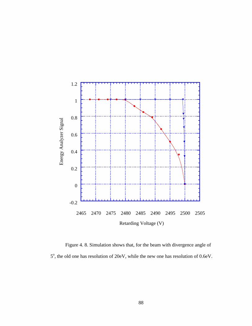
88
Figure 4. 8. Simulation shows that, for the beam with divergence angle of
5o, the old one has resolution of 20eV, while the new one has resolution of 0.6eV.
-0.2
0
0.2
0.4
0.6
0.8
1
1.2
2465 2470 2475 2480 2485 2490 2495 2500 2505
Ene
rgy
Ana
lyze
r Si
gnal
Retarding Voltage (V)

89
Figure 4. 9. Energy analyzer responses to a monogenetic beam at different
beam energy of 2.5 keV, 5.5 keV and 10 keV.
0
0.2
0.4
0.6
0.8
1
1.2
-3 -2.5 -2 -1.5 -1 -0.5 0 0.5
Ene
rgy
Ana
lyze
r Si
gnal
Retarding voltage relative to beam energy (V)
10 keV5.5 keV
2.5 keV
90
Figure 4. 10. Cross Section of new energy analyzer with cylindrical high
voltage electrode.
Electron Beam
Grounding Shield
High Voltage Cylinder
Collector
Signal Output
Mesh
Insulate Material
91
4.4 Beam Test of the New Energy Analyzer
4.4.1 Electron Gun Commissioning
In this experiment, the electron gun is the same as in the resistive–wall
experiment; but a new cathode is used. After commissioning, two experiments are
carried out to characterize the electron gun. The first experiment is to measure the
electron gun emission vs. filament heating power curve. This will help us to find
the optimized heating power for the cathode. If the heating temperature is too low,
the cathode is not uniformed heated and has poor emission. If the heating
temperature is too high, the emission will level off and the life-time of the cathode
will be much shortened. Because it takes long time for the cathode to reach the
thermal equilibrium, every time when we set different heating voltage, we have to
wait half an hour or longer for thermal equilibrium. Figure 4.11 shows the results
of the experiment. In the figure, the horizontal axis is the heating power and the
vertical axis is the electron gun current. The emission increases rapidly between 3.5
and 4 W of the heating power. After that point, the curve levels off. The cross
indicates the normal operating temperature, which corresponds to the heating
voltage of 6.6V. It is worth noting that the gun emission also depends on the
vacuum. Higher vacuum can result in better gun emission and longer cathode life-
time. In this experiment, the vacuum is kept at high 10-9 Torr.
The second experiment to characterize the electron gun is to study the gun
emission current vs beam energy at fixed A-K distance, 19 mm in the experiment.
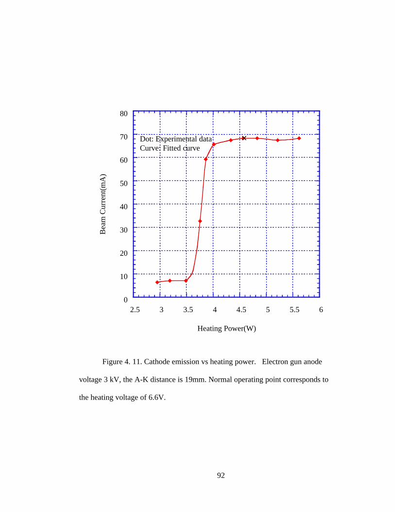
92
0
10
20
30
40
50
60
70
80
2.5 3 3.5 4 4.5 5 5.5 6
Bea
m C
urre
nt(m
A)
Heating Power(W)
Dot: Experimental dataCurve: Fitted curve
Figure 4. 11. Cathode emission vs heating power. Electron gun anode
voltage 3 kV, the A-K distance is 19mm. Normal operating point corresponds to
the heating voltage of 6.6V.
××
93
In this case, the heating voltage is set at 6.6 V, which is the normal operating
voltage determined previously. Figure 4.12 shows the results. In the figure, the
horizontal axis is the beam energy and the vertical one is the beam current. This
curve fitting shows that the beam current increases with the energy by power of
1.2. Ideally, this curve should follow Child-Langmuir law [44, 45], that is, the
current increases with the beam energy by the power of 1.5. This is based on the
one-dimensional model and planar-diode geometry. In this gun, due to this different
geometry, the emission is lower than this Child’s law limit.
The third test is to measure the beam current change vs the A-K distance.
The beam energy is fixed at 4.5 kV. Figure 4.13 shows the results. In the figure, the
current changes with the A-K distance by inverse power of 1.6. Again, this is lower
than the ideal case of inversely squared curve.
4.4.2 Experimental Apparatus
The experimental set up is shown in the Figure 4.14. Beam is emitted from
the electron gun and is focused by two solenoids down stream. The energy analyzer
is inside the first diagnostic chamber. A linear and rotation motion is used to adjust
the position of the energy analyzer accurately. Two solenoids are the same as in the
resistive-wall experiment. The distance of two solenoids and energy analyzer from
the electron gun is 9.1cm, 21.6 cm and 33.2 cm respectively. Figure 4.15 is one
example of the beam envelope in the transport line. Currents for the first and
94
second solenoids are 3.6 A and 4.7 A respectively. We can see that the energy
analyzer is sitting at the waist of the beam.
4.4.3 Test Results
Figure 4.16 is a typical signal output from the energy analyzer. In the
figure, the beam energy is 5 keV and the beam pulse length is 100 ns. From the
signal, we can see that this energy analyzer has pretty fast rise time (~2 ns) and can
reproduce the beam waveform faithfully.
The way to measure the energy spread of beam is to adjust the retarding
voltage and, by constructing the change of the beam current with the retarding
voltage, we can get the beam energy profile information. Figure 4.17 shows such a
case. In the figure, different traces corresponding to different retarding voltage are
plotted together. The traces of larger index number correspond to higher retarding
voltage. From this figure, the beam energy spread can be reconstructed, as shown
in figure 4.18. In this figure, the vertical axis is the beam current at the center of the
pulse and the horizontal axis is the retarding voltage. By taking the difference of
the data, the beam energy profile can be plotted, which is shown in figure 4.19. In
this example, the beam energy and current is 2.5 keV and 60 mA respectively. The
measured beam rms energy spread is 1.8 eV.
Tests are also performed at different beam energies. Figure 4.20 shows the
beam energy spread change with the beam energy. Notice, in this case, the beam
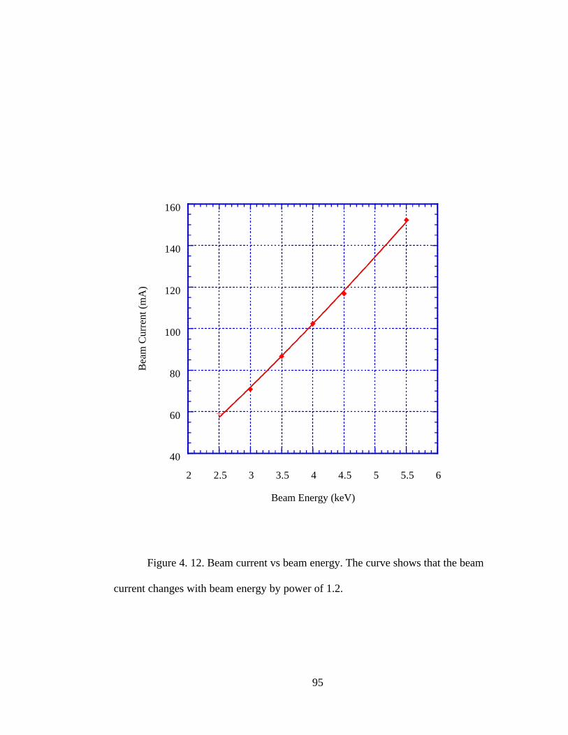
95
Figure 4. 12. Beam current vs beam energy. The curve shows that the beam
current changes with beam energy by power of 1.2.
40
60
80
100
120
140
160
2 2.5 3 3.5 4 4.5 5 5.5 6
Bea
m C
urre
nt (
mA
)
Beam Energy (keV)

96
Figure 4. 13. Electron gun emission current vs A-K distance. The curve
fitting gives that the current changes with the distance by inverse power of 1.6.
50
100
150
200
250
300
350
8 10 12 14 16 18 20 22 24
Bea
m C
urre
nt (
mA
)
A-K Distance (mm)

97
Figure 4. 14. Experimental setup for the energy analyzer test. M1, M2 and
M3 are the three solenoids.
Electron Gun
M1 M2 M3
Energy Analyzer
Vacuum Chamber
Linear and RotationFeedthrough
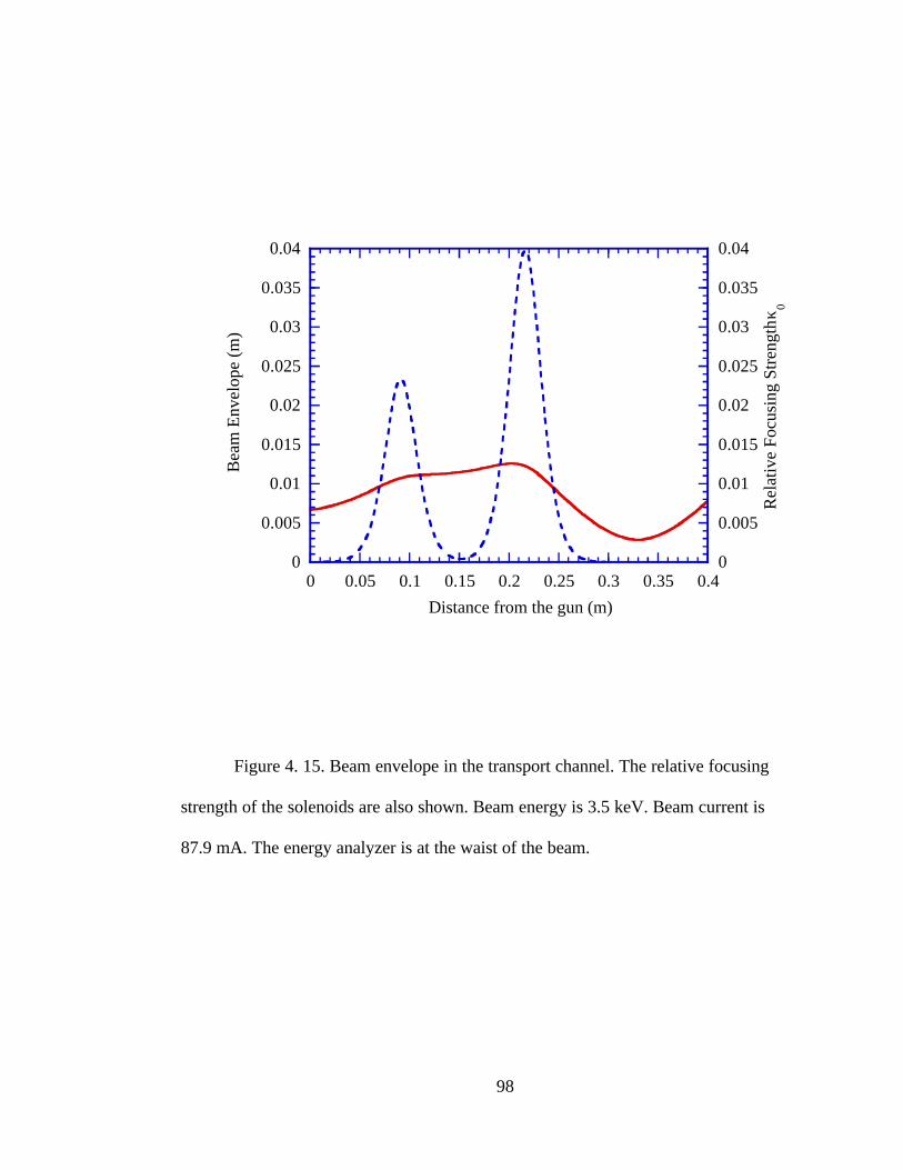
98
Figure 4. 15. Beam envelope in the transport channel. The relative focusing
strength of the solenoids are also shown. Beam energy is 3.5 keV. Beam current is
87.9 mA. The energy analyzer is at the waist of the beam.
0
0.005
0.01
0.015
0.02
0.025
0.03
0.035
0.04
0
0.005
0.01
0.015
0.02
0.025
0.03
0.035
0.04
0 0.05 0.1 0.15 0.2 0.25 0.3 0.35 0.4
Bea
m E
nvel
ope
(m)
Rel
ativ
e Fo
cusi
ng S
tren
gth κ
0
Distance from the gun (m)
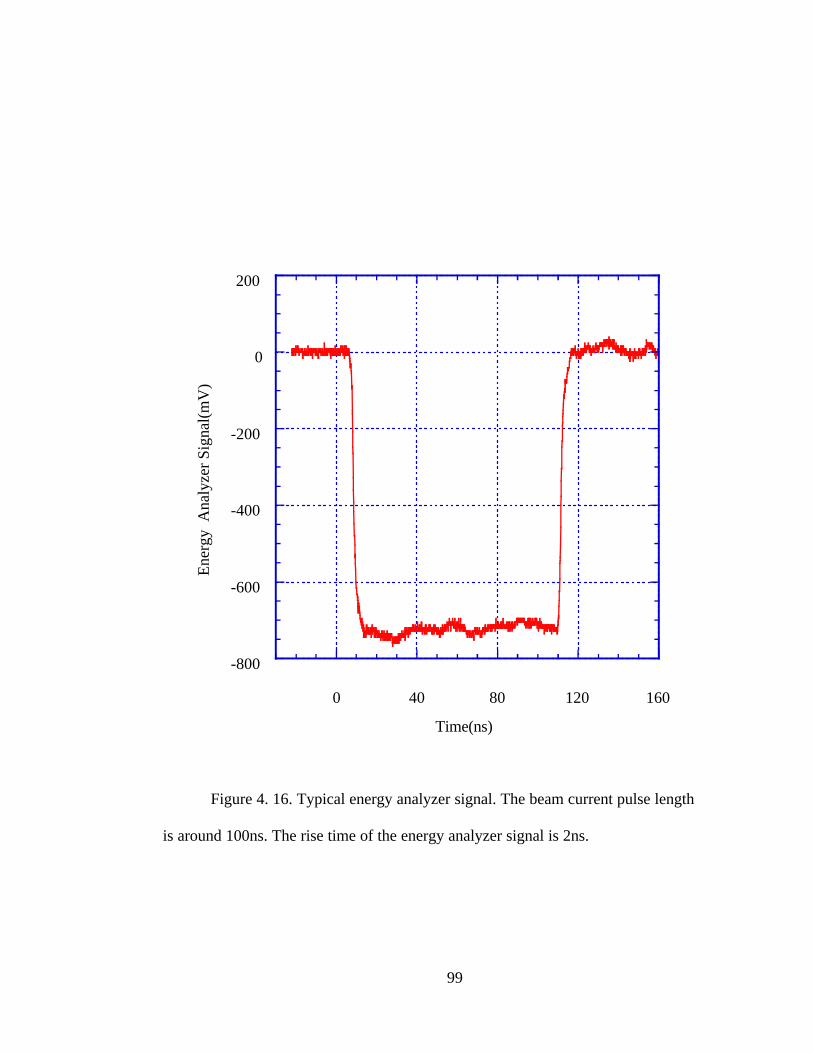
99
Figure 4. 16. Typical energy analyzer signal. The beam current pulse length
is around 100ns. The rise time of the energy analyzer signal is 2ns.
-800
-600
-400
-200
0
200
0 40 80 120 160
Ene
rgy
Ana
lyze
r Si
gnal
(mV
)
Time(ns)

100
Figure 4. 17. Different beam current waveforms at different retarding
voltages. Six waveforms are shown in the figure.
-800
-600
-400
-200
0
200
0 40 80 120 160
Ene
rgy
Ana
lyze
r Si
gnal
(mV
)
Time(ns)
(1)
(2)
(3)
(4)
(5)
(6)
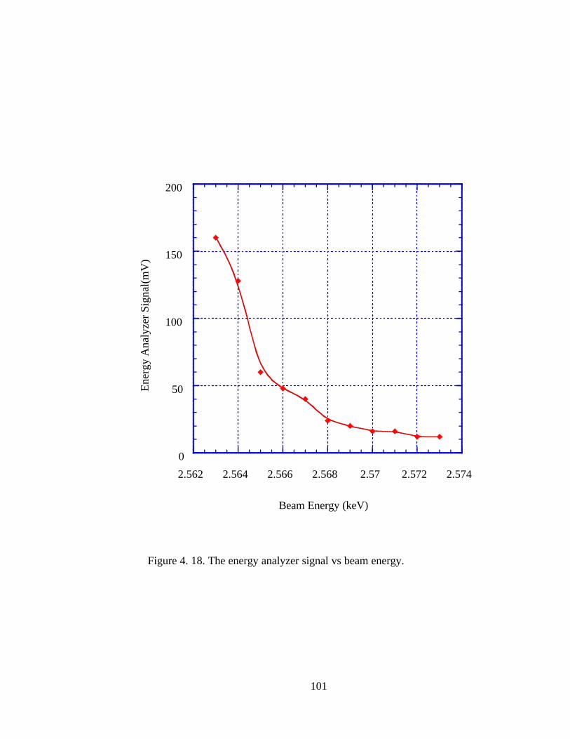
101
Figure 4. 18. The energy analyzer signal vs beam energy.
0
50
100
150
200
2.562 2.564 2.566 2.568 2.57 2.572 2.574
Ene
rgy
Ana
lyze
r Si
gnal
(mV
)
Beam Energy (keV)

102
Figure 4. 19. Beam energy distribution for a beam with energy 2.5 keV. The
rms energy width is 1.8 eV.
0
20
40
60
80
-4 -2 0 2 4 6 8
Rel
ativ
e N
umbe
r of
Par
ticle
s
Relative Beam energy (eV)
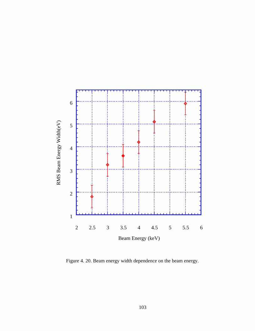
103
Figure 4. 20. Beam energy width dependence on the beam energy.
1
2
3
4
5
6
2 2.5 3 3.5 4 4.5 5 5.5 6
RM
S B
eam
Ene
rgy
Wid
th(e
V)
Beam Energy (keV)
104
current is not fixed. By Child’s law, the beam current increases with the beam
energy as shown in Figure 4.12.
4.5 Theoretical Considerations of the Sources of Beam Energy
Spread
The theoretical understanding of the evolution of energy spread in a beam is
very complicated and not complete. There are different papers and books
describing the energy broadening in a charged-particle beam [1, 31, 33-35]. Here I
give a brief review of two dominant sources of the energy spread and compare
them to the measurements in our experiment.
4.5.1 The Boersch Effect
When the beam is emitted from the cathode, it has energy spread due to the
cathode temperature. The rms beam energy spread is related to the temperature by
TkmvEE Brmsrms ==∆=∆ 2~. (4. 9)
Here, vrms is the rms thermal velociy, kB is the Boltzmann’s constant and T is the
beam temperature.
When the beam is accelerated by an electric field, every particle will gain
longitudinal kinetic energy. Suppose two particles having an energy difference ∆E
in the beginning. They will still have the same amount of energy difference ∆E
105
after acceleration. However, their velocity difference will change. To see the
difference between the velocity spread and energy spread, consider two non-
relativistic particles, one with initial velocity v1i, and the other one with initial
velocity v2i=v1i+∆vi. When they are accelerated through an acceleration gap of
voltage V0, the two particles will have final kinetic energy of
021
21 2
1
2
1qVmvmv if += (4. 10a)
and
02
1022
22 )(
2
1
2
1
2
1qVvvmqVmvmv iiif +∆+=+= . (4.10b)
The difference of the velocity after the acceleration, ∆vf, is defined as
mqVvmqVvvv iiif /2/2)( 0210
21 +−+∆+=∆ (4. 11)
By expanding both equations and assuming ∆v is much smaller than the mean
velocity, we find that
f
iif v
vvv
1
1∆=∆ . (4. 12)
From this relation, we find that the velocity difference between the particles is
smaller after the acceleration. Because the random velocity distribution is related to
the temperature, this effect is called the longitudinal cooling of the beam due to
acceleration [1].
106
This can also be viewed from the relation between the energy spread and
the temperature. Initially, the beam energy spread is given by Equation (4.9). After
acceleration, the beam thermal energy spread is [1]
fBf TkqVE ||02~
=∆ . (4. 13)
Here, V0 is the accelerating voltage, T||f is the longitudinal temperature after
acceleration. Because the energy spread in the lab system is the same before and
after the acceleration, equating Eqs.(4.13) and (4.9), we find that
0
2||
|| 2
)(
qV
TkTk iB
fB = . (4. 14)
Here, T||i is the initial beam temperature, which is isotropic (i.e. T||i=T⊥i=T) before
the acceleration. This longitudinal cooling effect is very significant. For example, if
initially the beam has a cathode temperature of 1100o C, corresponding to a thermal
energy of 0.1eV. After the electron beam has been accelerated to 5 keV, the
longitudinal temperature is decreased to 1×10⁻⁶eV, a reduction of temperature by a
factor of 105!
Note that the transverse temperature is the same as the initial temperature
since the acceleration acts only in the longitudinal direction. The longitudinal
temperature becomes negligible compared to the transverse temperature. The beam
is now in an extremely anisotropic state (T||i<<T⊥i). Coulomb collisions and other
processes will try to redistribute the beam velocity distribution into thermal
107
equilibrium. The transverse temperature is decreased while the longitudinal
temperature is increased. The resulting beam longitudinal energy spread will
increase. This thermal relaxation procedure is referred to as the Boersch Effect
because Boersch was the first researcher to observe this effect [See Ref [1], Chapter
6].
The transverse-longitudinal temperature relaxation effect is very
complicated in a real beam. For a simple case in which the beam propagates
through a smooth focusing channel and has a constant radius, the temperature
relaxation can be described by the following equations [1]
τ||||
2
1 TT
dt
dT
dt
dT −−=−= ⊥⊥ . (4. 15a)
constTTT eq ==+⊥ ||3
1
3
2(4.15 b)
Here, T|| and T⊥ are longitudinal and transverse temperature respectively. Teq is the
final equilibrium temperature. τ is the relaxation time. With the initial conditions
T||0=0 and T⊥0=3/2 Teq, we can solve these two equations and the solutions are
),2
11(
3
2 /30
effteTT τ−⊥⊥ += (4. 16a)
and ),1(3
2 /30||
effteTT τ−⊥ −= (4.16b)
where τeff is the effective temperature relaxation time and is given by
108
Λ×=
ln
)/(1044.4
2/3220
n
mcTk effBeffτ . (4. 17)
Here, Teff is related to T⊥0 by
0373.0 ⊥= TkTk BeffB . (4. 18)
lnΛ is the Coulomb logarithm and it is obtained from
×=Λ
2/1
2/3221 )/(
1066.5lnlnn
mcTkB . (4. 19)
In the formula, n is the particle density and is given by
vea
In
π2= , (4. 20)
where I is the beam current, a is the beam radius and v is the beam velocity.
From Equation (4.16), we find that the final longitudinal and transverse
temperature will reach the equilibrium of two thirds of the initial transverse
temperature. The time it takes to reach equilibrium is about τeff. Figure 4.21 shows
how they reach equilibrium with time. In the figure, longitudinal and transverse
temperatures are normalized to the final temperature and the time is normalized to
the effective relaxation time.

109
0
0.5
1
1.5
0 0.5 1 1.5 2
Nor
mal
ized
Tem
pera
ture
Normalized Time
Transverse Temperature
Longitudinal Temperature
Figure 4. 21. Relaxation of the transverse and longitudinal temperature due
to Boersch effect. The time is normalized to teff and the temperature is normalized
to ⊥T3
2.

110
4.5.2 The Longitudinal-Longitudinal Relaxation Effect
The energy transfer from transverse direction to longitudinal direction due
to the Boersch effect can be suppressed by applying a strong magnetic field.
However, even if this energy transfer is suppressed, the final beam energy spread is
found to be still larger than what is predicted by transverse-longitudinal cooling
effect. The reason is that the coulomb collisions in addition to the Boersch effect,
cause another temperature relaxation called longitudinal-longitudinal relaxation. If
the acceleration is fast (non-adiabatic) compared to the period of the electron beam
plasma oscillation period, the initial state of relative high density and slow motion
of electrons relative to each other is preserved during the acceleration process.
Coulomb collisions relax this non-equilibrium state into a more homogenous state
and result in energy spread increase. Taking into account this longitudinal-
longitudinal effect, the final beam energy spread is [1, 10]
2/1
||003/1
0|| 2
~
+=∆ TkqVqVqn
CE Bf πε
, (4. 21)
Here fE||
~∆ is the rms energy spread after acceleration and beam propagation; qV0 is
the beam energy and T|| is an increasing function of time or distance of beam
propagation, which can be calculated from Equation (4.16) (Boersch Effect). All
the beam energies are in units of eV; n is the beam density, q is the electron charge
and C is a constant of the order of unity. The first term in the bracket corresponds
to the longitudinal-longitudinal effect during acceleration, and the second term is
111
the transverse-longitudinal (Boersch) effect. The second term takes much longer
time than the first term until equilibrium between longitudinal temperature T|| and
transverse temperature T⊥ is reached. The Boersch effect (second term in Eq.
(4.21)) quickly dominates over the longitudinal-longitudinal relaxation effect.
To look at the time scale of the longitudinal-longitudinal effect, we first
have to calculate the plasma frequency of the beam. In the electron beam, the
plasma frequency can be expressed as
m
nqp
0
2
εω = . (4. 22)
Here n is the particle density, m is the electron mass, q is the electron charge and ε0
is the dielectric constant. In our experiment, ωp is typically about 7.8×10⁸ s-1 and
one plasma period is
pωπτ /2= , (4. 23)
which is around 8 ns, a very short time. While for a similar beam, the effective
relaxation time constant of the Boersch effect is in the range of microseconds.
As was pointed out before, the longitudinal-longitudinal effect occurs when
the beam acceleration is fast (non-adiabatic) and it can be reduced by adiabatic
acceleration. The criteria for the adiabaticity condition is determined by a non-

112
dimensional parameter λ, which compares the cooling time
1
||
||
1−
−
dt
dT
T with the
plasma period ωp-1:
dt
dT
Tp
||
||
1
ωλ −= . (4. 24)
If λ<1, then the acceleration is adiabatic. λ depends on the acceleration structure. It
is interesting to note that a thermal electron gun with Pierce geometry has λ equal
to 23/2 [10], a nonadiabatic case, which applies to our experiment.
4.5.3 Comparison of the Experimental Results with the Energy Spread
Predicted by the above two Sources.
We can use the above theory to estimate the energy spread due to the
Boersch effect and the longitudinal-longitudinal effect. In our example, the beam
energy ranges from 2.5 keV to 5.5 keV. The beam is emitted from a cathode with
radius of 5 mm. In the transport system, the average beam radius is around 9 mm.
By applying Equations (4.16)~(4.17) to a 2.5 keV beam with beam current of 60
mA, we calculate that the rms energy spread due to the Boersch effect is ~1.0 eV.
The first term of Equation (4.21) gives the energy spread due to the longitudinal-
longitudinal effect, which is 0.9 eV in this case. The final energy spread resulting
from both effects as given by Equation (4.21), is ~1.3 eV. The experimental
measurement of the energy spread for this 2.5 keV beam is 1.8 eV, relatively close

113
to, but larger than, the theoretical prediction. The measurements are also performed
at different beam energies. Table 4.2 shows the comparison of the results from
these two effects and the results from experiments. The table shows that at this
distance, the energy spreads due to the two sources are comparable. From the
comparison, we find that the experimental results are always larger than the
theoretical predictions, and the discrepancy increases with beam energy. The
discrepancy becomes larger at higher beam energy. There are several possible
reasons for this discrepancy. First, as we explained earlier, the resolution of the
energy analyzer decreases almost linearly with increasing energy. Secondly,
besides these two dominant energy spread sources, there are other sources which
may cause an increase of the beam energy spread. For example, some simulations
show that a beam with a two-temperature anisotropy (T||i<<T⊥i) will develop an
instability which will increase the longitudinal energy spread and even significantly
deteriorate the beam quality [41,42].
Table 4. 2. Comparison of the rms energy spread from sources of Boersch
effect, longitudinal-longitudinal effect and experiment at different beam energies.
Beam Energy(keV)
Boersch Effect(eV)
L-L Effect(eV)
Combination ofBoth Effects (eV)
ExperimentalResults (eV)
2.5 1.0 0.9 1.3 1.83 1.1 1.0 1.5 3.23.5 1.2 1.1 1.6 3.64 1.3 1.2 1.8 4.24.5 1.4 1.3 1.9 5.15.5 1.6 1.4 2.1 5.9
114
4.6 A Computer-Controlled System for Energy Spread
Measurements
Measuring beam energy spread is very tedious and time consuming because
it needs a lot data taking and processing. In the previous experiment, we could not
afford taking a lot data points because, to save the cathode lifetime, we can only
keep the beam running for a short time. After we are familiar with running
experiment, it becomes natural and necessary to run the experiment automatically.
A computer-controlled system is designed for this purpose. The system diagram is
shown in Figure 4.22. The software platform is LabVIEWTM 5.0. A high voltage is
supplied by an analog high-voltage power supply; the analog power supply can be
controlled by a computer through Bertan 205B GPIB interface. Bertan 205B takes
the GPIB command from the computer and converts it into analogue signal to
control the high voltage power supply. The analog signal is 0~10 V for the full
range control.
The Tektronix 602A Digital Signal Analyzer (DSA) takes the data from the
energy analyzer and saves the data to disk for later processing. The DSA has a
GPIB interface so it is easy to communicate with the computer. In the experiment,
the user set high voltage scanning range and the DSA channel number on the
software front panel. The data file name and whether or not you want to save the
data can also be set in the beginning. User also has to set the time window for
which she wants to measure the energy profile. After clicking RUN button, the
115
program will start to set the high voltage, take the energy analyzer data and set new
high voltage and take data again. The process keeps going until full high voltage
range has been scanned. After the data are taken, the software will plot out the
energy profile and its differentiation for the beam energy distribution. Figure 4.23
shows the front panel of the demo program.
The automated system works much faster than doing it manually. The
measurement speed of this system is mainly limited by saving signal trace to the
disk. So user has an option to choose fast mode or slow mode. In the fast mode, the
data is only taken in the memory, but not saved to the disk. In the slow mode, all
the traces are stored in the disk. Approximately 50 data points can be taken in four
minutes when the system runs in the fast mode, while 20 data points can be taken in
four minutes in the slow mode.
The system still needs improvement. In the experiment, we found that the
real high voltage output is always a couple of volts off from the setting value. We
guess this is due to the analog control of the high voltage power supply. Because in
the analog control, we use 0~10 V control signal to control 0~10 kV high voltage.
If there is any voltage drop due to the connection resistance, the output voltage will
be smaller than the setting voltage. One way to correct this problem is to make
good contact of each connector. However, this has limited effect. A better solution
is to use a digital interface directly in the high voltage power supply and use TTL
signal to control the power supply.

116
Figure 4. 22. Computer-controlled system for retarding voltage energy
analyzer.
DSA 602A
200-c488high voltagecontroller
Berta
ncable
Computer( LabVIEW)
GPIB Cable
GPIB cable GPIB cable
Energy Analyzer
high voltage cable
coaxial cable
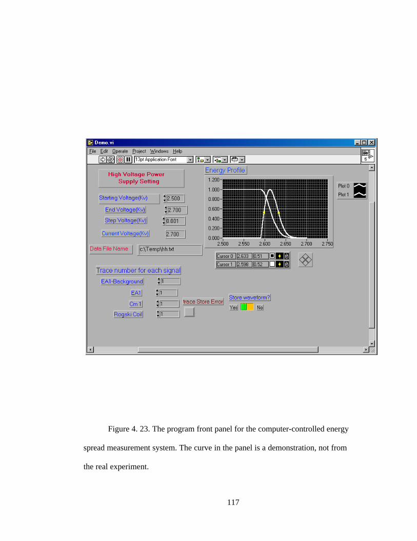
117
Figure 4. 23. The program front panel for the computer-controlled energy
spread measurement system. The curve in the panel is a demonstration, not from
the real experiment.
118
4.7 Conclusion and Future Work
Work has been performed to study the principle of retarding voltage energy
analyzer. It was found that due to the imperfection of the energy analyzer, the
response of the energy analyzer is not always the same as in the ideal case. The
objective of designing an energy analyzer is to get as close as possible the ideal
response to a real beam.
Performances of different retarding voltage energy analyzer were studied
and compared. Study showed that the parallel energy analyzer developed
previously is only good for measuring the highest energy of the beam but not good
enough to measure the beam energy spread. The transverse beam trajectories will
affect the energy analyzer results and result in apparently larger energy spread. A
new energy analyzer with cylindrical structure was designed to improve the
resolution of energy spread measurement. Computer simulation showed that it has
much better resolution than the parallel energy analyzer.
Beam test was performed on the cylindrical energy analyzer. The new
experiment has achieved much smaller energy spread than the previous
experiments, showing that the results are much closer to the real beam energy
spread. Measurements were also performed at different beam energy to study the
energy width dependence on the beam energy.
119
Simples models were applied to estimate the energy spread in the electron
beam due to the Boersch effect and longitudinal-longitudinal effect. The
experimental results and the theory estimation agreed reasonably well.
The computer simulation and beam test showed that this energy analyzer is
good enough to be used for UMER and future study of the energy spread in the
space-charge-dominated beam. This includes the electron gun characterization,
resistive-wall instability in UMER and more systematic measurement of the beam
energy spread at different distance from the electron gun and with different beam
parameters etc. In the experiment, we also found that the new energy analyzer is
very reliable and very robust with respect to the mechanical misalignment.
A computer-controlled system is being built to run experiment more
efficiently.
120
Chapter 5
Development of a Capacitive Beam Position Monitor (BPM)
and a Fast Rise-Time Dipole for the University of Maryland
Electron Ring (UMER)
5.1 The University of Maryland Electron Ring (UMER)
To study the physics of space-charge dominated beams, a small electron
ring has been designed and being built at the University of Maryland [5, 30, 36]. It
is directly motivated by the research in the heavy ion inertial fusion (HIF), which
requires extremely high-density and short-pulse beam. As a cost-saving alternative,
beam physics of the intense heavy ion beam could be studied on a low-energy
electron ring. Compared to the linear accelerator, the electron ring can be small
enough to fit into a regular laboratory while still can provide much longer beam
path to study the dynamics of space-charge dominated beam.
The schematic of the UMER is shown in Figure 5.1. A 10 keV, 100mA, 70-
100 ns electron beam with a normalized effective emittance of 10 mm-mrad from
an electron gun is injected into the ring with the aid of a pulsed, Panofsky-type
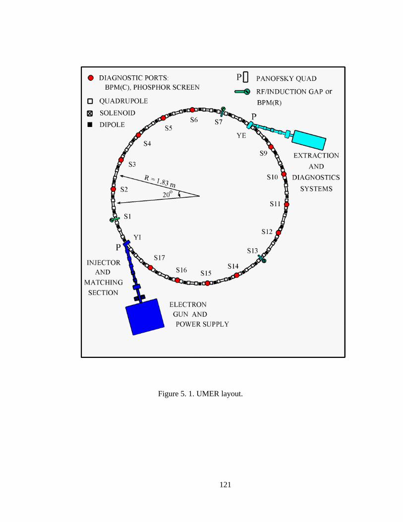
121
Figure 5. 1. UMER layout.
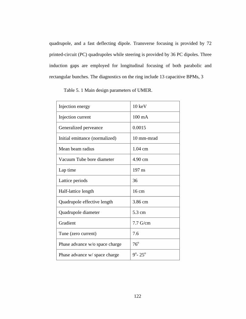
122
quadrupole, and a fast deflecting dipole. Transverse focusing is provided by 72
printed-circuit (PC) quadrupoles while steering is provided by 36 PC dipoles. Three
induction gaps are employed for longitudinal focusing of both parabolic and
rectangular bunches. The diagnostics on the ring include 13 capacitive BPMs, 3
Table 5. 1 Main design parameters of UMER.
Injection energy 10 keV
Injection current 100 mA
Generalized perveance 0.0015
Initial emittance (normalized) 10 mm-mrad
Mean beam radius 1.04 cm
Vacuum Tube bore diameter 4.90 cm
Lap time 197 ns
Lattice periods 36
Half-lattice length 16 cm
Quadrupole effective length 3.86 cm
Quadrupole diameter 5.3 cm
Gradient 7.7 G/cm
Tune (zero current) 7.6
Phase advance w/o space charge 76o
Phase advance w/ space charge 9o- 25o

123
resistive-wall current monitors and 13 phosphor screens. A pulsed extraction
system similar to the injector is included for beam analysis. The extraction chamber
houses an emittance meter, an energy analyzer and a phosphor screen viewer. The
ring’s main parameters are summarized in Table 5.1.
5.2 Development of a Capacitive Beam Position Monitor (BPM)
5.2.1 Motivation
BPMs, including capacitive BPMs and resistive BPMs, are widely used in
charged particle accelerators and beam lines [37-39]. In the UMER, because the
beam has relatively low energy (10 keV), it is almost impossible to have the beam
perfectly centered in the pipe. Every imperfection, like stray magnetic fields (the
earth’s field and other stray fields due to the presence of metal) and misalignments
of the quadupoles and dipoles, will let the beam go off-centered. To guarantee the
success of the UMER, beam centroid motion has to be measured very accurately
and the information from the BPMs must be provided to a beam steering system to
steer the beam back. Both resistive wall BPMs and capacitive BPMs will be used in
the UMER. The detailed theory and design of a capacitive BPM are discussed
below.
124
5.2.2 Basic Principle
The common method of monitoring the position of a charged-particle beam
is to couple the electromagnetic field of the beam. When an electron beam travels
inside a beam pipe, there are electromagnetic fields accompanying it. For a highly
relativistic beam, the fields are pure transverse electric and magnetic fields. In our
case, the beam energy is 10 keV and it is non-relativistic. However, the beam is so
long that the fields accompanying the beam body are still transverse fields, which
means that one-dimensional model is still a good approximation for this problem.
There are two types of most commonly used, non-interceptive BPMs in the
accelerator field. One is called resistive-wall BPM, which is a gap in the beam pipe
with a ceramic sealing to maintain vacuum. A bunch of uniformly distributed
resistors are connected across the gap to carry the wall currents. The azimuthal
distribution of wall currents, determined by the voltage across different resistors,
can be used to measure the beam position. Another way to detect the
electromagnetic field of a beam is to put a pair of electrodes inside the beam pipe.
When the beam passes an electrode, signals are induced on it. Based on the
different signals from two opposite electrodes, we are able to determine the beam
position. Because this is a capacitive pick up, it is referred as capacitive BPM in the
linterature. In this section, we will focus on the design of a capacitive BPM.
There are various kinds of electrodes for capacitive BPM. Button electrode,
which is short and the capacitance is very small, is suitable for detecting very weak
125
beam current. On the other hand, capacitive electrode, which is relatively long and
has larger capacitance, can reproduce the beam pulse waveform faithfully. We use
the second structure because it is very important for us to see the beam profile
while measuring the beam position. This becomes essential when we study the
propagation of space charge waves in the beam.
Figure 5.2(a) is a sketch of the cross section of a capacitive BPM. There are
four pickup electrodes uniformly located inside the beam pipe. If the beam is
centered, the induced voltage on each electrode are the same. First, let us study the
response of an arbitrary electrode to a centered beam.
Assume the beam current is Ib(t), and the electrode is short enough that the
current inside can be treated as independent of the z position, the induced charge
on one of the electrode can be written as
)(20
/),(2
)(0
0 tb
Iv
LLvdzzt
bItQ
πα
πα
≅∫= . (5. 1)
Here, L is the electrode length, α is the angle of the electrode, Ib(t) is the beam
current and v0 is the beam velocity. If the capacitance between the electrode and
beam pipe is C, then the voltage on the electrode due to the induced charge is given
by
bI
Cv
L
C
QV
02πα
== , (5. 2)
where C is given by

126
CR1
Is
IL
v
dI t
dtsb=
Φ2 0π
( )
Figure 5. 2. (a) BPM pick up electrodes. (b) BPM equivalent circuit.
Right Electrode
X
Y
Φy
x
r
θ
Top Electrode
Left Electrode
Bottom Electrode
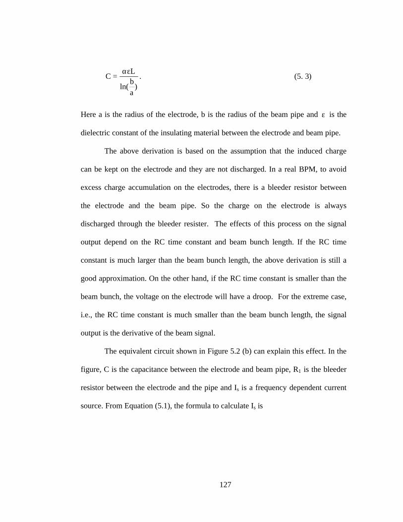
127
CLb
a
=αε
ln( ). (5. 3)
Here a is the radius of the electrode, b is the radius of the beam pipe and ε is the
dielectric constant of the insulating material between the electrode and beam pipe.
The above derivation is based on the assumption that the induced charge
can be kept on the electrode and they are not discharged. In a real BPM, to avoid
excess charge accumulation on the electrodes, there is a bleeder resistor between
the electrode and the beam pipe. So the charge on the electrode is always
discharged through the bleeder resister. The effects of this process on the signal
output depend on the RC time constant and beam bunch length. If the RC time
constant is much larger than the beam bunch length, the above derivation is still a
good approximation. On the other hand, if the RC time constant is smaller than the
beam bunch, the voltage on the electrode will have a droop. For the extreme case,
i.e., the RC time constant is much smaller than the beam bunch length, the signal
output is the derivative of the beam signal.
The equivalent circuit shown in Figure 5.2 (b) can explain this effect. In the
figure, C is the capacitance between the electrode and beam pipe, R1 is the bleeder
resistor between the electrode and the pipe and Is is a frequency dependent current
source. From Equation (5.1), the formula to calculate Is is
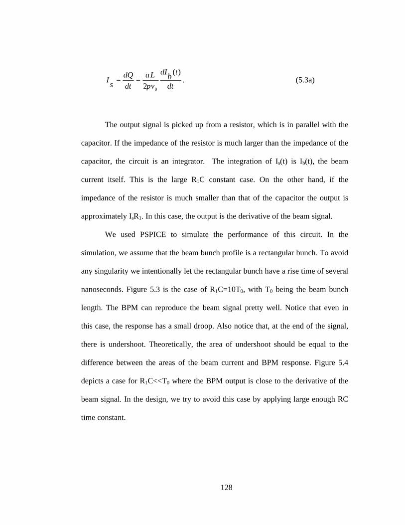
128
dt
tb
dI
v
L
dt
dQs
I)(
2 0πα
== . (5.3a)
The output signal is picked up from a resistor, which is in parallel with the
capacitor. If the impedance of the resistor is much larger than the impedance of the
capacitor, the circuit is an integrator. The integration of Is(t) is Ib(t), the beam
current itself. This is the large R1C constant case. On the other hand, if the
impedance of the resistor is much smaller than that of the capacitor the output is
approximately IsR1. In this case, the output is the derivative of the beam signal.
We used PSPICE to simulate the performance of this circuit. In the
simulation, we assume that the beam bunch profile is a rectangular bunch. To avoid
any singularity we intentionally let the rectangular bunch have a rise time of several
nanoseconds. Figure 5.3 is the case of R1C=10T0, with T0 being the beam bunch
length. The BPM can reproduce the beam signal pretty well. Notice that even in
this case, the response has a small droop. Also notice that, at the end of the signal,
there is undershoot. Theoretically, the area of undershoot should be equal to the
difference between the areas of the beam current and BPM response. Figure 5.4
depicts a case for R1C<<T0 where the BPM output is close to the derivative of the
beam signal. In the design, we try to avoid this case by applying large enough RC
time constant.
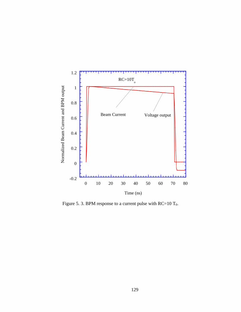
129
Figure 5. 3. BPM response to a current pulse with RC=10 T0.
-0.2
0
0.2
0.4
0.6
0.8
1
1.2
0 10 20 30 40 50 60 70 80
Nor
mal
ized
Bea
m C
urre
nt a
nd B
PM o
utpu
t
Time (ns)
Beam Current Voltage output
RC=10To
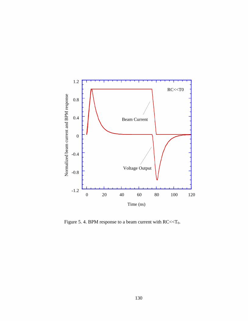
130
Figure 5. 4. BPM response to a beam current with RC<<T0.
-1.2
-0.8
-0.4
0
0.4
0.8
1.2
0 20 40 60 80 100 120
Nor
mal
ized
bea
m c
urre
nt a
nd B
PM r
espo
nse
Time (ns)
Beam Current
Voltage Output
RC<<T0
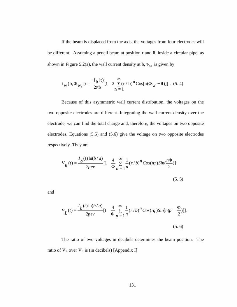
131
If the beam is displaced from the axis, the voltages from four electrodes will
be different. Assuming a pencil beam at position r and θ inside a circular pipe, as
shown in Figure 5.2(a), the wall current density at b, Φw is given by
iw b w tIb t
br b n Cos n
nw( , , )
( )[ ( / ) [ ( )]]Φ Φ=
−+
=
∞∑ −
21 2
1πθ . (5. 4)
Because of this asymmetric wall current distribution, the voltages on the
two opposite electrodes are different. Integrating the wall current density over the
electrode, we can find the total charge and, therefore, the voltages on two opposite
electrodes. Equations (5.5) and (5.6) give the voltage on two opposite electrodes
respectively. They are
)]2
()1
()/(14
1[2
)/ln()()(
Φ∑∞
=Φ+=
nSin
nnCosnbr
nv
abtb
It
RV θ
πε
(5. 5)
and
)]]2
([)1
()/(14
1[2
)/ln()()(
Φ+∑
∞
=Φ+= πθ
πεnSin
nnCosnbr
nv
abtb
It
LV .
(5. 6)
The ratio of two voltages in decibels determines the beam position. The
ratio of VR over VL is (in decibels) [Appendix I]
132
20160
10
2 20
10
8
3
3
2 162
2
128
3
3 23
3
38
3
2 162
2
2
3
log( / )ln
( / )
ln[
( )( )Sin( / )
( / )] [
( )( )Sin( / )
] ...
VR VLSin x
b
SinSin
Sin x
b
SinSin xy
b
= + −
+ + − + +
ΦΦ
Φ
ΦΦ Φ
Φ
Φ
Φ
Φ
ΦΦ Φ
Φ
.
(5. 7)
If x/b is small enough, we can take the linear term. It is
20160
10
2log( / )
ln
( / )VR VL
Sin x
b=
ΦΦ
. (5. 8)
The above formula shows that the logarithmic ratio of two voltages is
proportional to the beam position. The coefficient of the linear term is called the
sensitivity of the BPM, the parameter that we are most interested in. The coefficient
of the second term in Equation (5.7) is the nonlinearity of the BPM. We can
compensate this term by calibrating the BPM on the x or y axis. The third term,
which depends on both x and y displacements, is the coupling term between x and
y direction.
It is interesting to note that the coefficient of each term only depends on the
electrode angular width Φ . Figure 5.5 gives the plots of these terms with respect to
the angle Φ . From this figure we find that the sensitivity and the nonlinear term
decrease with Φ , but both of them are greater than zero if Φ is between zero and
133
Figure 5. 5. The dependence of different terms on the electrode angle width.
-4
-2
0
2
4
0 20 40 60 80
Rel
ativ
e St
reng
th o
f D
iffe
rent
Ter
ms
Electrode Angle (Degree)
Sensitivity term
Nonlinear term
Coupling term
134
90o. The coupling term, however, could be positive or negative, depending on Φ .
So it is possible to let the coupling term be zero by using an appropriate electrode
width Φ . From Equation (5.7), let the third term be zero, i.e.
− + =8
3
2 162
20
Sin Sin Sin( ) ( ) ( / )Φ
ΦΦ Φ
Φ. (5. 9)
By solving this equation, we get Φ =76.99o. If we set the electrode width to be
76.99o, we are able to decouple the signals from X and Y electrodes.
5.2.3 Design and Bench Test of a Prototype BPM
A prototype capacitive BPM has been designed and built to test our theory.
The geometry is the same as in Figure 5.2(a). There are four electrodes inside the
pipe, which are insulated from the grounded pipe by mylar, a material with
dielectric constant of 2.9 ε0 . Each electrode is connected to a bleeder resistor R.
For the bench test, a conducting cylindrical bar was built to simulate the beam. The
bar and pipe form a co-axial structure with 50 Ω impedance. The bar can move
freely inside the pipe. A pulser provides a 100 mA current pulse on the bar. The
pulse is terminated by a 50 Ω load, as shown in Figure 5.6.
The signal is picked up from the bleeder resistor, which has a resistance of 3
kΩ. Because this resistor is very large, we have to use 1-MΩ impedance channel in
the oscilloscope in order to avoid any interference with the source. The problem
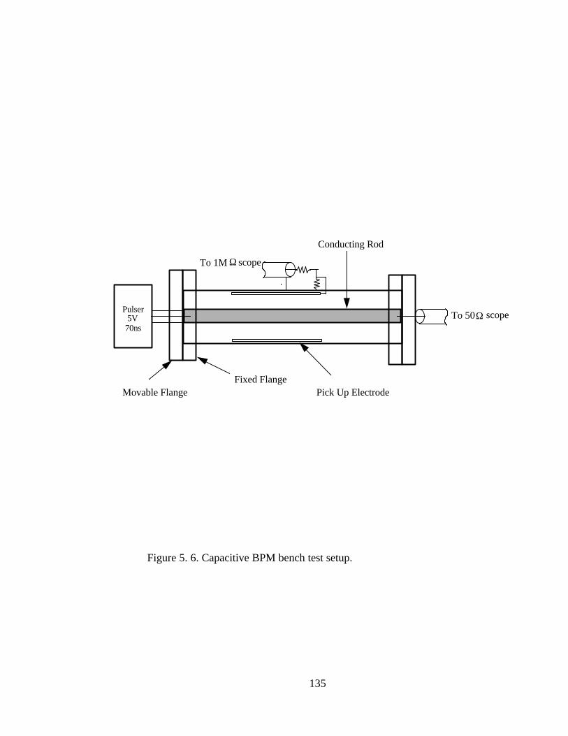
135
Pulser5V
70ns
To 1M Ω scope
To 50Ω scope
Fixed FlangeMovable Flange Pick Up Electrode
Conducting Rod
Figure 5. 6. Capacitive BPM bench test setup.
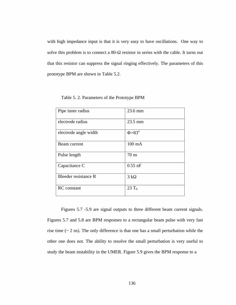
136
with high impedance input is that it is very easy to have oscillations. One way to
solve this problem is to connect a 80-Ω resistor in series with the cable. It turns out
that this resistor can suppress the signal ringing effectively. The parameters of this
prototype BPM are shown in Table 5.2.
Table 5. 2. Parameters of the Prototype BPM
Pipe inner radius 23.6 mm
electrode radius 23.5 mm
electrode angle width Φ=83o
Beam current 100 mA
Pulse length 70 ns
Capacitance C 0.55 nF
Bleeder resistance R 3 kΩ
RC constant 23 T0
Figures 5.7 -5.9 are signal outputs to three different beam current signals.
Figures 5.7 and 5.8 are BPM responses to a rectangular beam pulse with very fast
rise time (~ 2 ns). The only difference is that one has a small perturbation while the
other one does not. The ability to resolve the small perturbation is very useful to
study the beam instability in the UMER. Figure 5.9 gives the BPM response to a
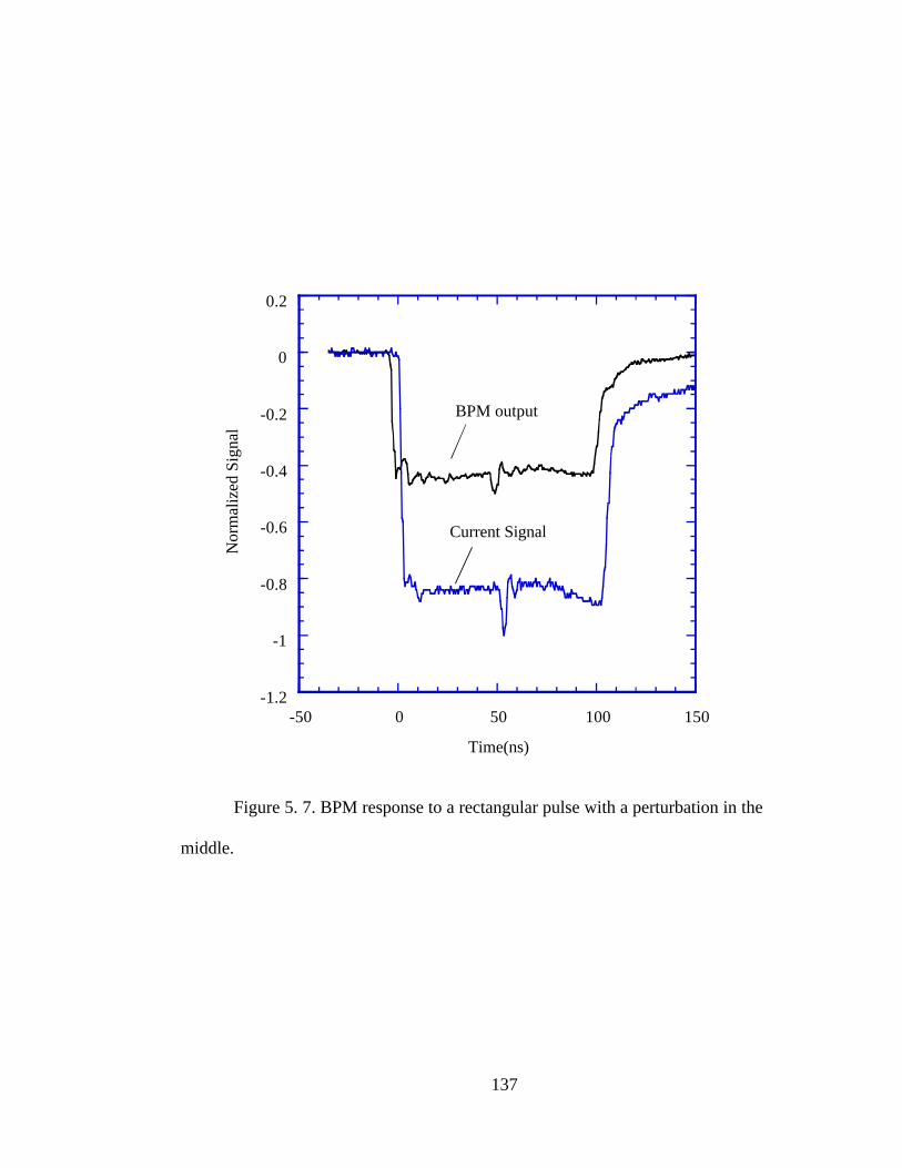
137
Figure 5. 7. BPM response to a rectangular pulse with a perturbation in the
middle.
-1.2
-1
-0.8
-0.6
-0.4
-0.2
0
0.2
-50 0 50 100 150
Nor
mal
ized
Sig
nal
Time(ns)
BPM output
Current Signal

138
Figure 5. 8. BPM response to a rectangular pulse with fast rise-time.
-0.2
0
0.2
0.4
0.6
0.8
1
1.2
-40 -20 0 20 40 60 80 100
Nor
mal
ized
Sig
nal
Time(ns)
Current Signal
BPM output
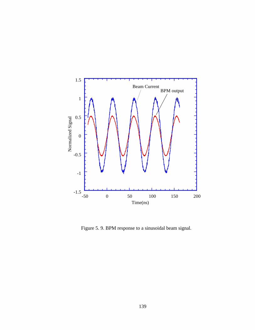
139
Figure 5. 9. BPM response to a sinusoidal beam signal.
-1.5
-1
-0.5
0
0.5
1
1.5
-50 0 50 100 150 200
N
orm
aliz
ed S
igna
l
Time(ns)
Beam CurrentBPM output
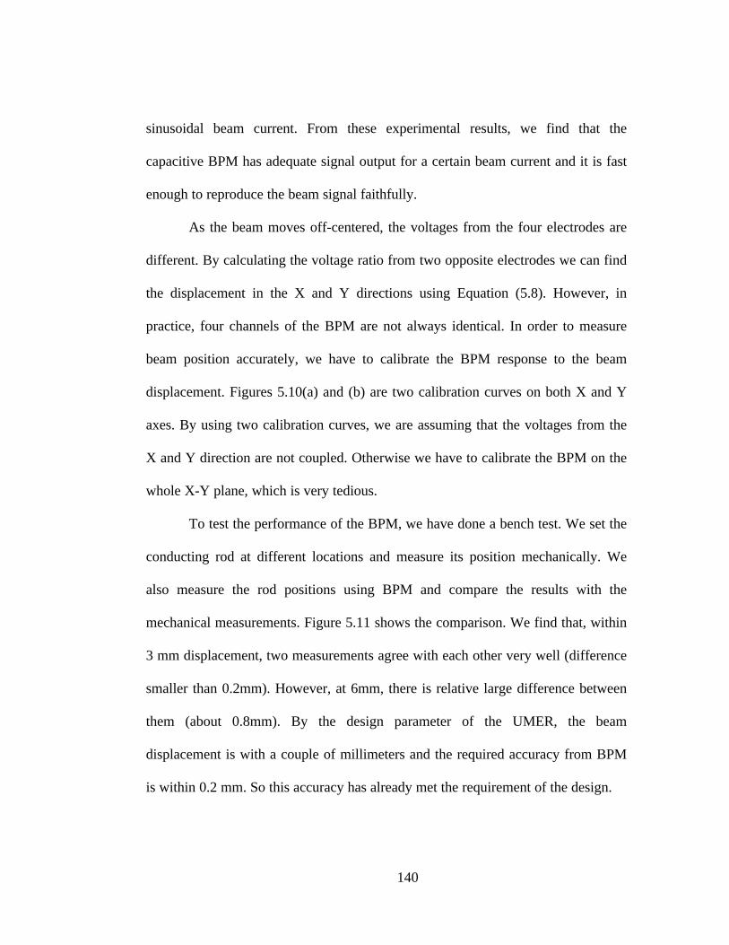
140
sinusoidal beam current. From these experimental results, we find that the
capacitive BPM has adequate signal output for a certain beam current and it is fast
enough to reproduce the beam signal faithfully.
As the beam moves off-centered, the voltages from the four electrodes are
different. By calculating the voltage ratio from two opposite electrodes we can find
the displacement in the X and Y directions using Equation (5.8). However, in
practice, four channels of the BPM are not always identical. In order to measure
beam position accurately, we have to calibrate the BPM response to the beam
displacement. Figures 5.10(a) and (b) are two calibration curves on both X and Y
axes. By using two calibration curves, we are assuming that the voltages from the
X and Y direction are not coupled. Otherwise we have to calibrate the BPM on the
whole X-Y plane, which is very tedious.
To test the performance of the BPM, we have done a bench test. We set the
conducting rod at different locations and measure its position mechanically. We
also measure the rod positions using BPM and compare the results with the
mechanical measurements. Figure 5.11 shows the comparison. We find that, within
3 mm displacement, two measurements agree with each other very well (difference
smaller than 0.2mm). However, at 6mm, there is relative large difference between
them (about 0.8mm). By the design parameter of the UMER, the beam
displacement is with a couple of millimeters and the required accuracy from BPM
is within 0.2 mm. So this accuracy has already met the requirement of the design.
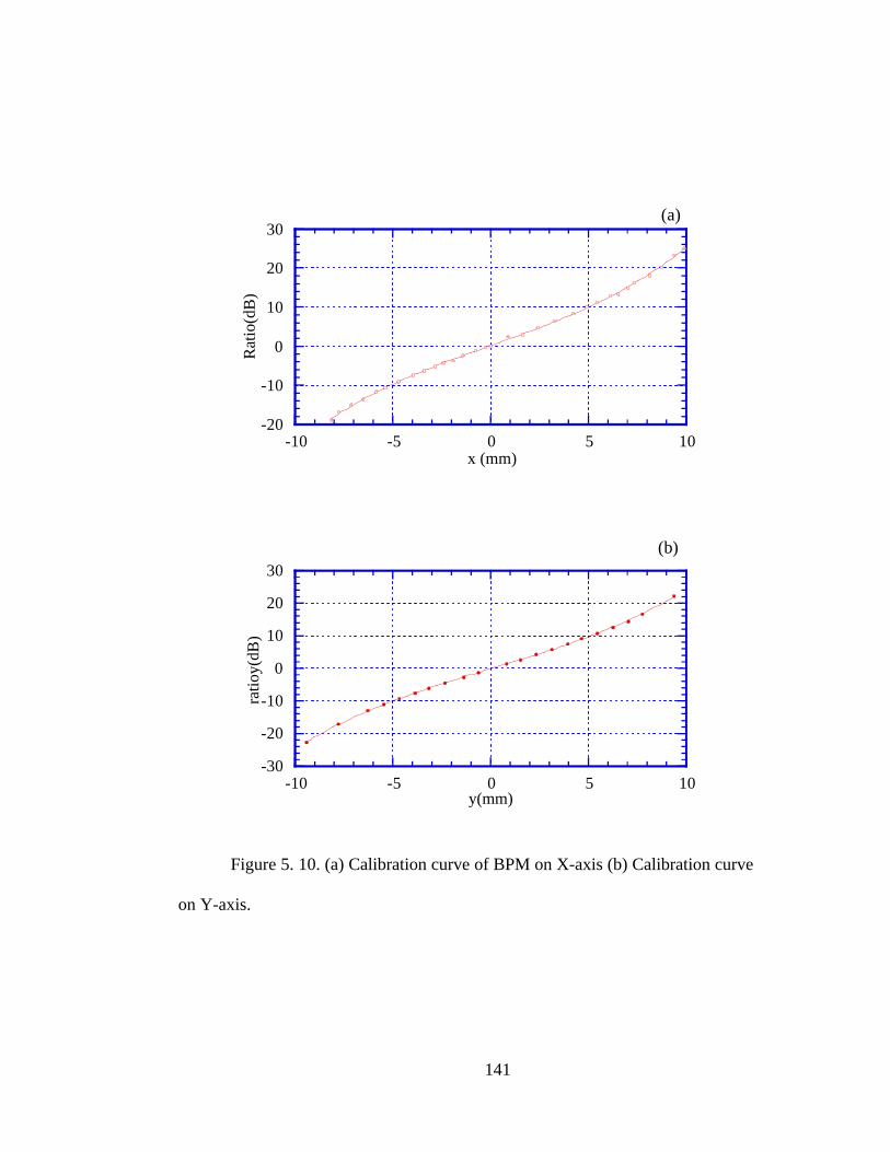
141
Figure 5. 10. (a) Calibration curve of BPM on X-axis (b) Calibration curve
on Y-axis.
-20
-10
0
10
20
30
-10 -5 0 5 10
Rat
io(d
B)
x (mm)
(a)
-30
-20
-10
0
10
20
30
-10 -5 0 5 10
ratio
y(dB
)
y(mm)
(b)
142
Figure 5. 11. Comparison of BPM measurements and mechanical
measurements. They agree well within 3 mm displacement. Due to the coupling
between X and Y electrodes, BPM gives larger results at larger beam offset.
-1
0
1
2
3
4
5
6
7
-1 0 1 2 3 4 5 6 7
Y (
mm
)
X (mm)
Dot: BPM MeasurementCross: Mechanical Measurment

143
Even though, it is interesting to study the source of the errors. Note that this
discrepancy is a systematic error and it is due to the coupling between the X and Y
electrodes, which is the third term in Equation (5.7). We expect this systematic
error will be smaller if we optimize the electrode angle to 77o.
After all, it is important to point out that, in the bench test, the signal on the
rod is a TEM wave with transverse electric or magnetic field, travels at the velocity
of light, which emulates highly relativistic particles. For a 10 keV beam, the
particle velocity is about 0.2 of the speed of light. As was shown in the formula, the
response of the BPM to a real beam will be larger than in the bench test case.
5.2.4 BPM Data Acquisition and Electronics
In the bench test, four BPM signals are hooked up to an oscilloscope
directly and are digitized for processing. In the UMER, there are 18 BPMs
altogether, so we have to design a data acquisition system to digitize and process
the totally 64-channel signals. Basically, there are two methods to process the
signal. A wide band system will contain all the frequency component of the signal;
while a narrow band system will only pick up certain frequency component of the
signal and process it. Each of the system has its own advantages and disadvantages.
Because it keeps all the frequency components, the wide band system can record
the system waveform faithfully. However, in this kind of system, the signal-to-
noise ratio is relative poor and the beam position accuracy is not as good as a
narrow band system. On the other hand, the narrow band system has better signal-
144
to-noise ratio and can measure the beam position as accurately as micrometers. The
disadvantage is that it can not reproduce the beam waveform because of its narrow
bandwidth.
In the UMER, the required beam position is about 0.3 mm within 3 mm
displacement. We are also very interested in using the BPM to measure the beam
current and beam waveform. So wide band system is used in the UMER BPM
system. For the design purpose, a very important thing is to determine the
bandwidth requirement of the system. The system should have enough bandwidth
to keep the fine structure of the beam signal, for example, the perturbation of space-
charge wave. Figure 5.12 is a typical beam current with perturbation and its
Fourier transform. Figure 5.12b shows that the frequency spectrum drops to –70dB
at 400 Mhz. A low pass filter with bandwidth 400 Mhz is designed to see how it
will affect the beam signal. Figure 5.13 is the spectrum of an ideal low pass filter.
Applying this filter to the original beam current signal, we get the signal after
filtering. Figure 5.14 plots both original signal and the filtered signal. We find that
there is little difference between two signals. This shows that the bandwidth of 400
Mhz is good enough for the BPM system.
Because, intrinsically, the BPM output has high impedance, we need a
buffer to transform its high impedance to 50 Ω impedance, which is the impedance
of the rest of the system. For this purpose, we use a preamplifier with high input
impedance and unity gain. The preamplifier was developed by Electronics Group at
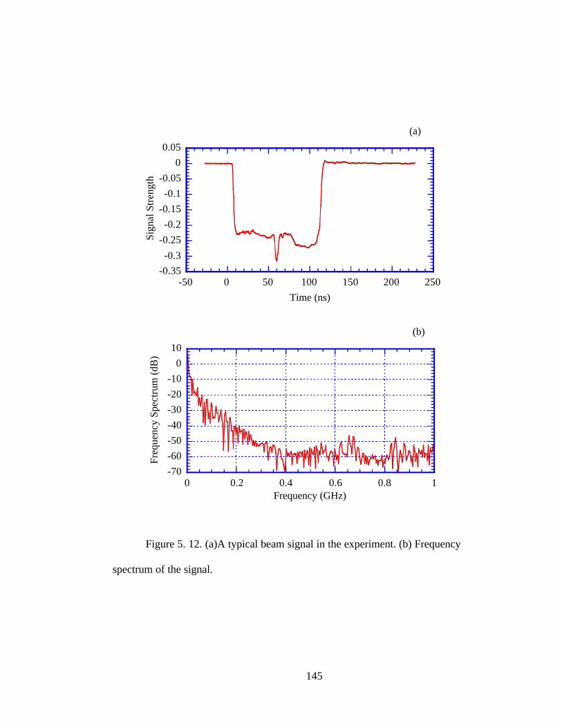
145
Figure 5. 12. (a)A typical beam signal in the experiment. (b) Frequency
spectrum of the signal.
-0.35
-0.3
-0.25
-0.2
-0.15
-0.1
-0.05
0
0.05
-50 0 50 100 150 200 250
Sign
al S
tren
gth
Time (ns)
(a)
-70
-60
-50
-40
-30
-20
-10
0
10
0 0.2 0.4 0.6 0.8 1
Freq
uenc
y Sp
ectr
um (
dB)
Frequency (GHz)
(b)

146
Figure 5. 13. Frequency response of an ideal low pass filter with pass
bandwidth 400 MHz.
-50
-40
-30
-20
-10
0
10
0 0.2 0.4 0.6 0.8 1
Am
plitu
de (
dB)
Frequency (GHz)

147
-0.35
-0.3
-0.25
-0.2
-0.15
-0.1
-0.05
0
0.05
-50 0 50 100 150 200 250
Sign
al S
tren
gth
(V)
Time (ns)
Figure 5. 14. (a) The original signal and its filtered signal. They are almost
identical. (b) The difference of the original signal and filtered signal.
-0.01
-0.005
0
0.005
0.01
0.015
-50 0 50 100 150 200 250
Dif
fere
nces
of
two
sign
als
(V)
Time (ns)
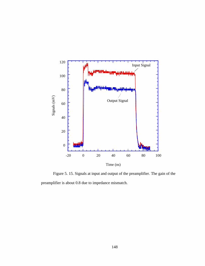
148
Figure 5. 15. Signals at input and output of the preamplifier. The gain of the
preamplifier is about 0.8 due to impedance mismatch.
0
20
40
60
80
100
120
-20 0 20 40 60 80 100
Sign
als
(mV
)
Time (ns)
Input Signal
Output Signal

149
Figure 5. 16. Layout for BPM data acquisition system.
Computer(LabVIEW)
BPM1
BPM2
RF Multiplexer
BPM18
Ch 1
Ch 2
Ch 3
Ch 4
Digitizer & Waveform
Analyzer
Data Bus
Preamplifier

150
Physics department, University of Maryland. The main part of the circuit is a MAX
4005 single-ended unity-gain buffer. The input is a high impedance JFET and the
output impedance is 75 Ω. By the data sheet, this buffer can also drive 50 Ω
transmission line with only a slight loss in amplitude. This preamplifier is tested
using a fast signal generator. Figure 5.15 plots the results. In the figure, the input
signal and output signal are plotted together. We can see this preamplifier has very
good bandwidth and fast rise-time. The tested gain is about 0.8.
Figure 5.16 shows the lay out for BPM data acquisition system. Right after
the BPM is a preamplifier described above. There are totally 64 channels of signal,
so a commercial RF multiplexer is used to multiplex the signals into a four-channel
digitizer. The digitized signals are thereafter transferred to the computer for
processing.
5.3 Study of a Fast Rise-time Deflecting Dipole
5.3.1 Motivation
In the UMER, the injection line has an angle of 20o with respect to the main
ring. Figure 5.17 shows the junction part of the injection line and the ring. When
the beam is injected into the ring, it will be deflected by –10o. After one turn, when
the beam comes back to the injection position, it has to be deflected by +10o, which

151
is the regular deflecting angle in the ring. At this junction part, we need a fast rise-
time dipole, which can flip its polarity in about 100 ns. This requires that the dipole
must have very small inductance so that its rise-time is within 50 ns. This imposes
the main challenge to the design of this dipole. Figure 5.18 gives the time sequence
of the field produced by the dipole. In the figure, we assume that the beam will run
10 turns in the ring. So the total time for the dipole to be on is about 2 µs.
5.3.2 Basic Configuration
It is well known that accurate multipole fields can be generated using
conductors placed in parallel to the axis in such a way that the current distribution
follows a cos(nθ) distribution, where n=1 for dipole and 2 for quadrupole, and θ is
the azimuthal angle. The main dipoles in the UMER are based on this principle and
were designed by FMT Inc.[40]. In the study of this fast dipole, we adopted the
same method using printed-circuit wires to produce the desired field. In order to
obtain small inductance, we use a combination of parallel and series structure. The
whole region is divided into four quadrants. In each quadrant, the conductors are
connected in parallel and the four quadrants are connected in series.
In the real design, each conductor carries equal current, and we have to
locate the position of the conductor sinusoidally to achieve the dipole field.
Suppose we use total number of nt conductors in one quadrant. First, we divide the

152
Figure 5. 17. Injection line of UMER.
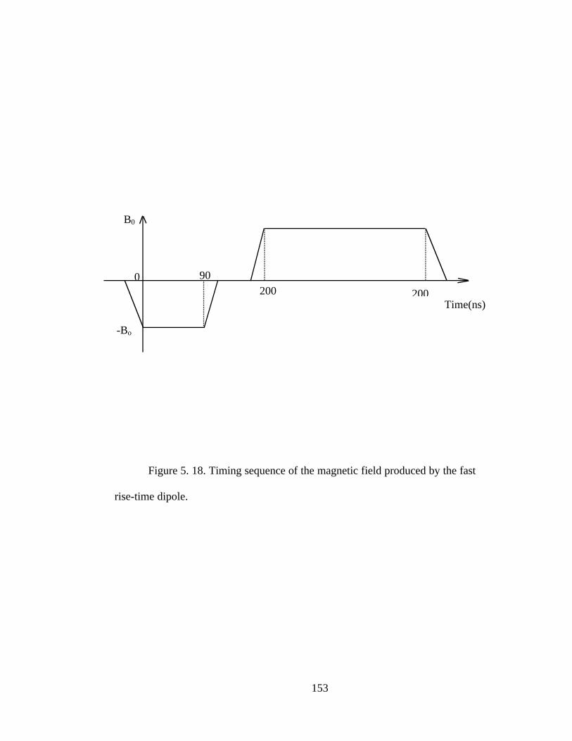
153
Figure 5. 18. Timing sequence of the magnetic field produced by the fast
rise-time dipole.
B0
Time(ns)
0 90200 200
-Bo
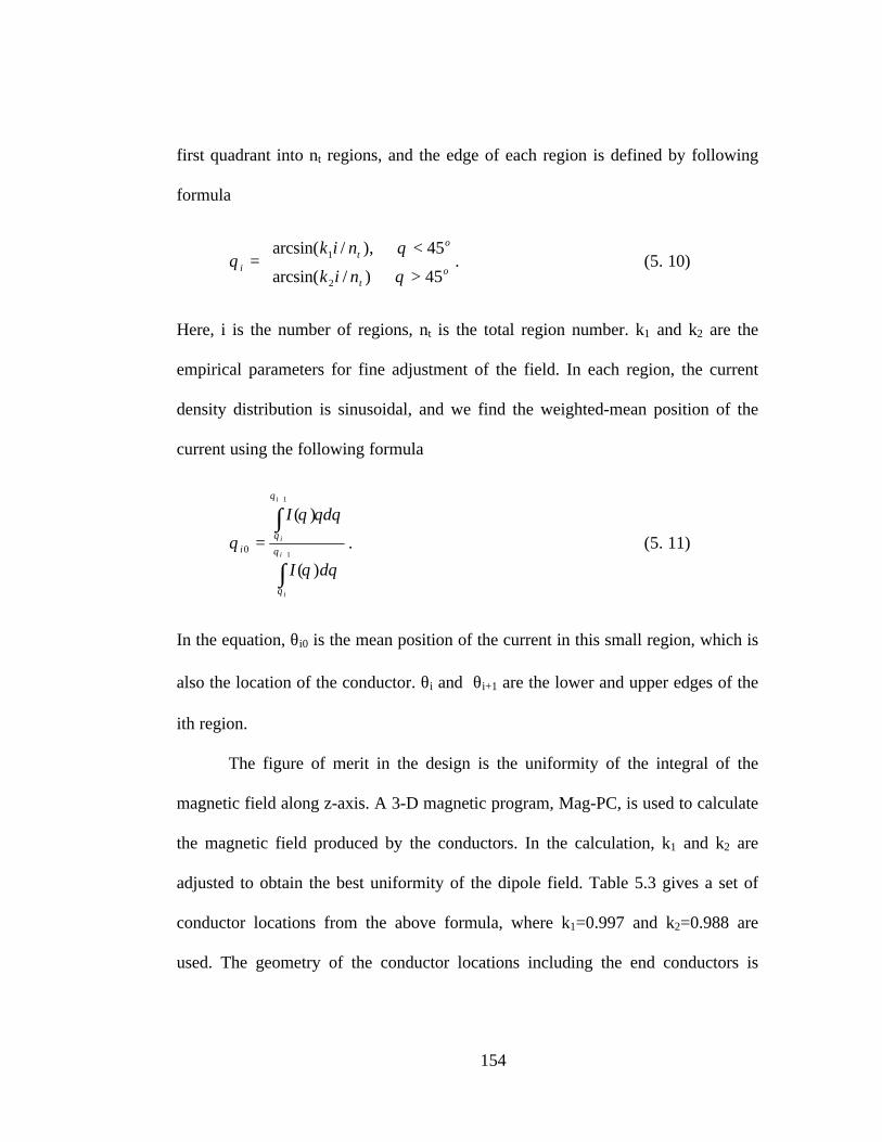
154
first quadrant into nt regions, and the edge of each region is defined by following
formula
>
<=
ot
ot
inik
nik
45)/arcsin(
45),/arcsin(
2
1
θ
θθ . (5. 10)
Here, i is the number of regions, nt is the total region number. k1 and k2 are the
empirical parameters for fine adjustment of the field. In each region, the current
density distribution is sinusoidal, and we find the weighted-mean position of the
current using the following formula
∫
∫+
+
=1
1
)(
)(
0i
i
i
i
dI
dI
i θ
θ
θ
θ
θθ
θθθ
θ . (5. 11)
In the equation, θi0 is the mean position of the current in this small region, which is
also the location of the conductor. θi and θi+1 are the lower and upper edges of the
ith region.
The figure of merit in the design is the uniformity of the integral of the
magnetic field along z-axis. A 3-D magnetic program, Mag-PC, is used to calculate
the magnetic field produced by the conductors. In the calculation, k1 and k2 are
adjusted to obtain the best uniformity of the dipole field. Table 5.3 gives a set of
conductor locations from the above formula, where k1=0.997 and k2=0.988 are
used. The geometry of the conductor locations including the end conductors is
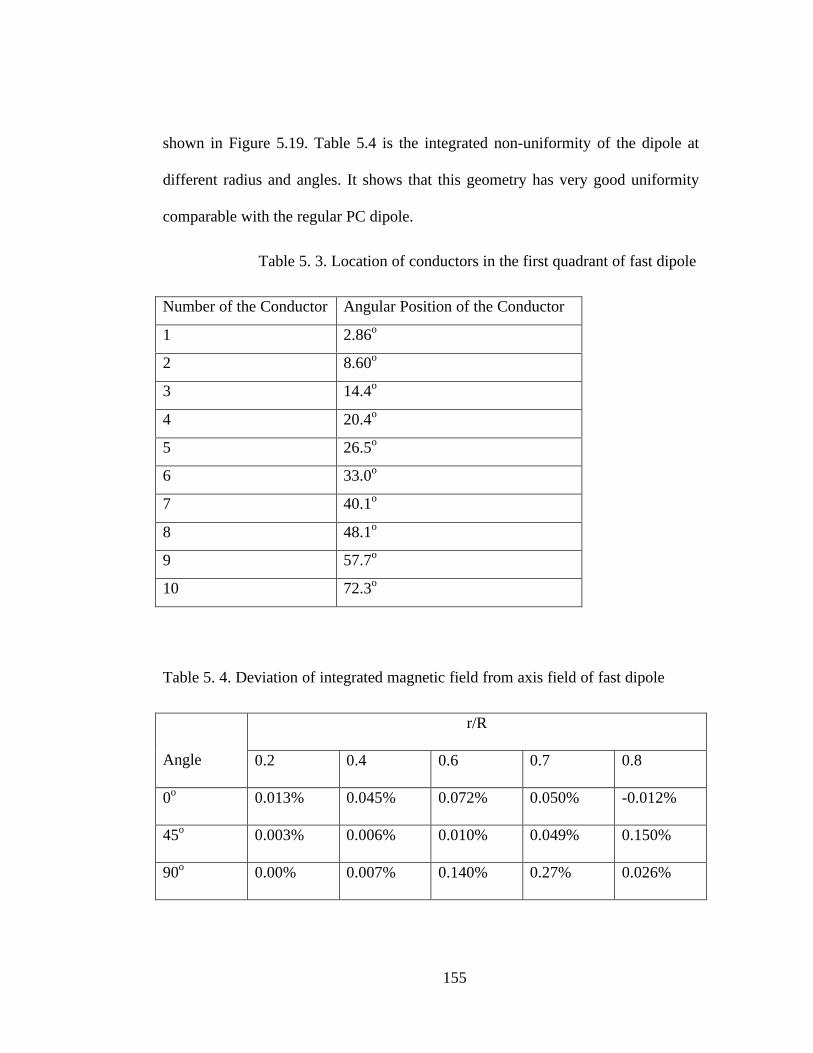
155
shown in Figure 5.19. Table 5.4 is the integrated non-uniformity of the dipole at
different radius and angles. It shows that this geometry has very good uniformity
comparable with the regular PC dipole.
Table 5. 3. Location of conductors in the first quadrant of fast dipole
Number of the Conductor Angular Position of the Conductor
1 2.86o
2 8.60o
3 14.4o
4 20.4o
5 26.5o
6 33.0o
7 40.1o
8 48.1o
9 57.7o
10 72.3o
Table 5. 4. Deviation of integrated magnetic field from axis field of fast dipole
r/R
Angle 0.2 0.4 0.6 0.7 0.8
0o 0.013% 0.045% 0.072% 0.050% -0.012%
45o 0.003% 0.006% 0.010% 0.049% 0.150%
90o 0.00% 0.007% 0.140% 0.27% 0.026%
156
Figure 5. 19. Position of conductors along the azimuthal angle.
Azimuthal angle
-180o 180o0o
157
The inductance of this geometry is very small. Based on the two
dimensional classical electrodynamics, we can estimate that the inductance of the
dipole is about 1.23×10⁻⁷ H/m. The detailed derivation of the inductance is shown
in Appendix II.
Figure 5.20 is a typical magnetic field profile on axis. The radius of the
dipole is 2.5 cm and the length of the dipole is 5 cm, which yields an aspect ratio of
one. The peak magnetic field of the dipole is 0.195 Gauss/A and the integrated field
along the axis is 58.8 Gauss-cm.
5.3.3 Inductance and Magnetic Field Measurement of a Prototype Model
To test the inductance and the field quality of this geometry, a prototype
fast dipole is made. The conductor distribution of the model is the same as in Table
5.3. But the aspect ratio is larger, which is about 1.75. To guarantee that each
conductor carries the same current, there is an accurate resistor connected in series
with each conductor. The total effective resistance of the dipole is 50 Ω for the
matching purpose.
A low voltage testing was performed to measure the inductance of this
prototype model. The circuit is shown in Figure 5.21. In the figure L and R are the
inductance and resistance of the dipole respectively. A fast pulse generator drives
the dipole with a fast rise-time, rectangular pulse, as shown in Figure 5.22a. The
signal is picked up from the resistor and is transmitted to the scope. Due to the
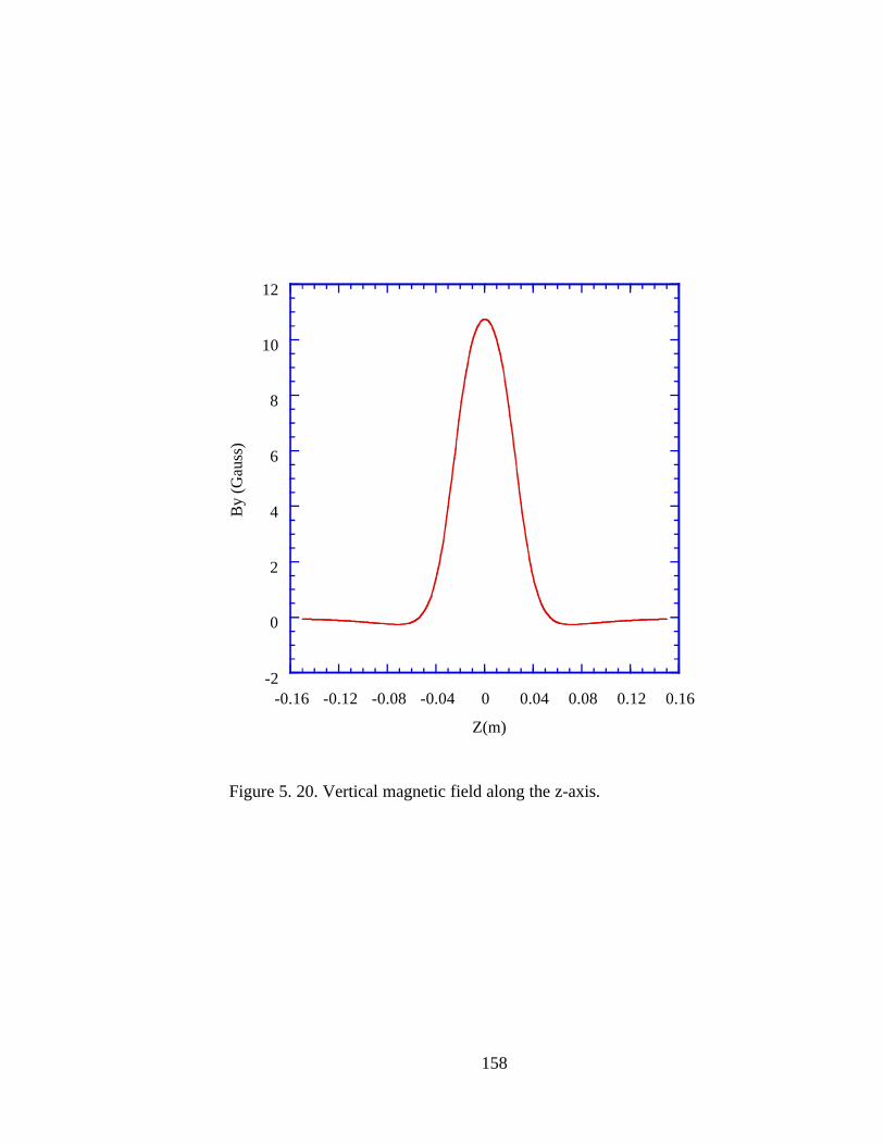
158
Figure 5. 20. Vertical magnetic field along the z-axis.
-2
0
2
4
6
8
10
12
-0.16 -0.12 -0.08 -0.04 0 0.04 0.08 0.12 0.16
By
(Gau
ss)
Z(m)
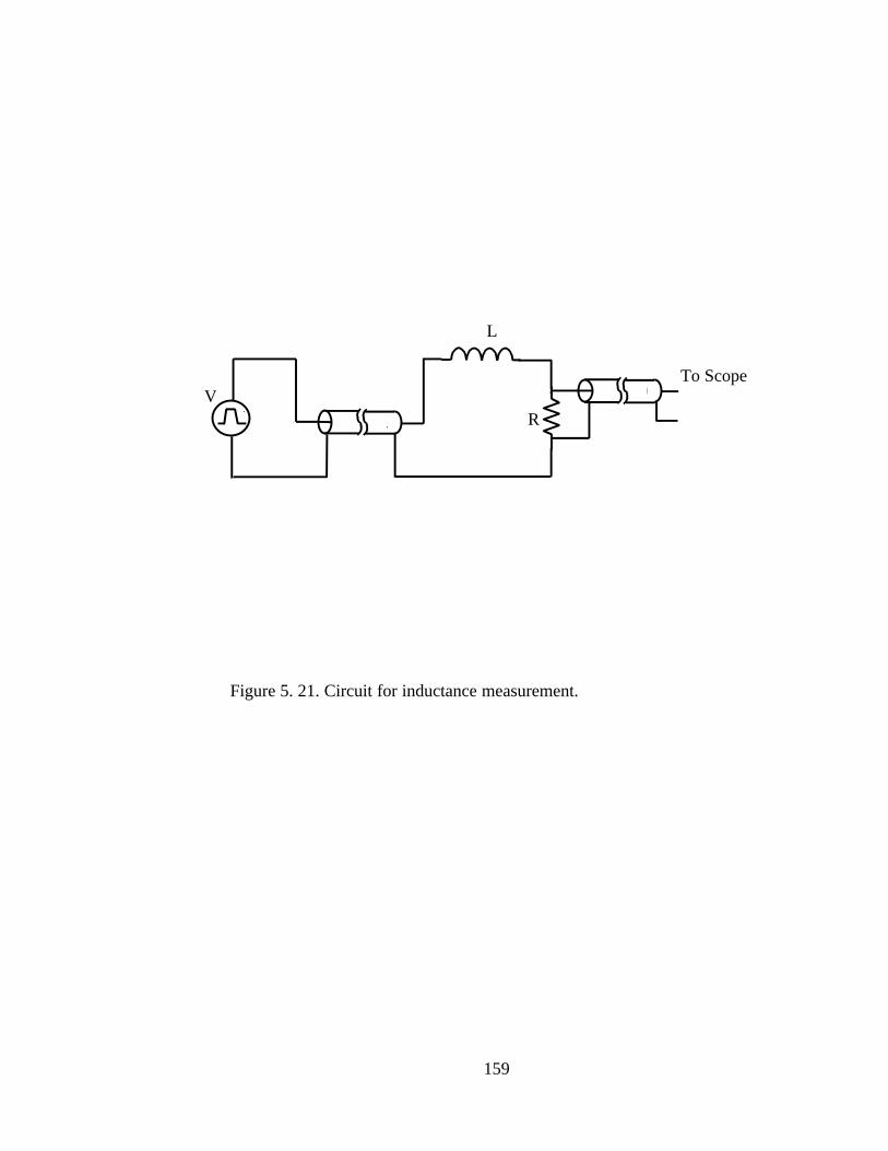
159
Figure 5. 21. Circuit for inductance measurement.
V
L
R
To Scope
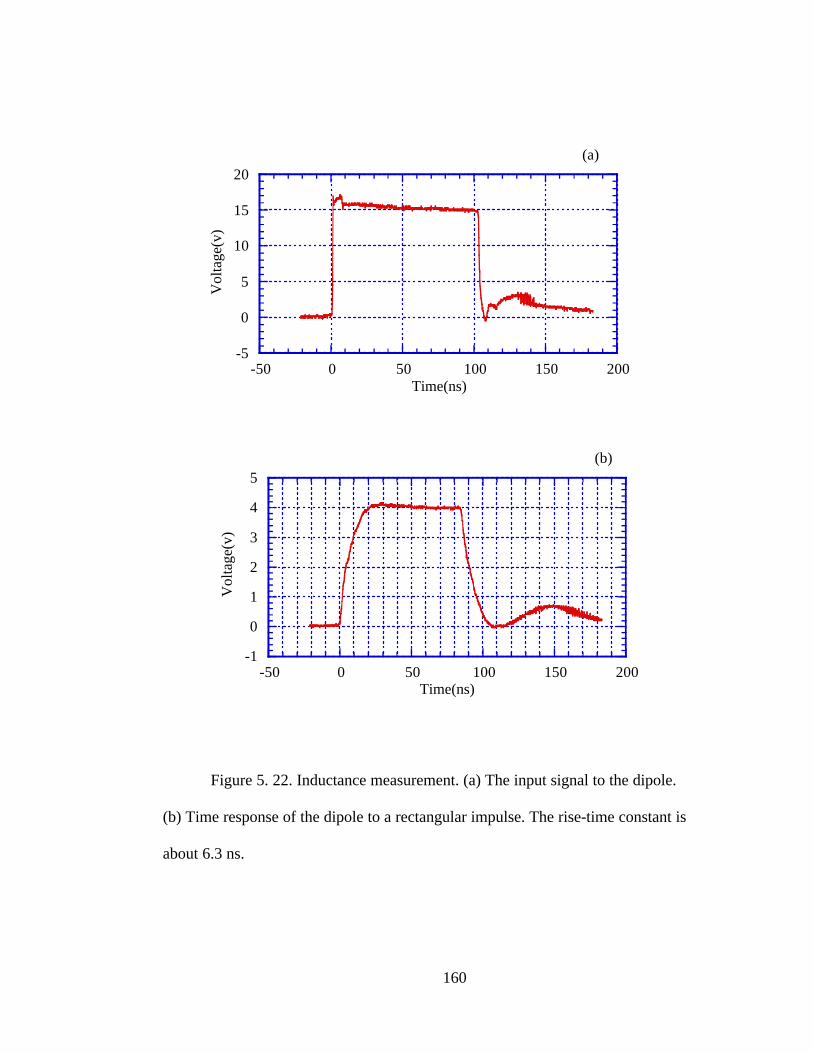
160
Figure 5. 22. Inductance measurement. (a) The input signal to the dipole.
(b) Time response of the dipole to a rectangular impulse. The rise-time constant is
about 6.3 ns.
-5
0
5
10
15
20
-50 0 50 100 150 200
Vol
tage
(v)
Time(ns)
(a)
-1
0
1
2
3
4
5
-50 0 50 100 150 200
Vol
tage
(v)
Time(ns)
(b)
161
inductance of the dipole, the rise time in the dipole is longer than the original
signal. From the rise-time of the current in the dipole, we are able to measure the
inductance of the dipole. Figure 5.23b shows the current signal in the dipole. The
rise-time constant of the current τ is about 6.4 ns. The resistance of the circuit is 50
Ω, which yields the inductance of the dipole L=Rτ is about 0.32 µH. As was
discussed previously, the calculated inductance per unit length for this dipole is
1.23×10⁻⁷ H/m, and because we connect the four quadrants in series, the inductance
is 16 times larger. The length of the dipole is 0.16 m, so the total calculated
inductance of the prototype dipole is about 0.315 µH, very close to the
measurement.
The measurement of the magnetic field of the dipole is tricky. Because the
inductance of the dipole is so small, the magnetic field is very difficult to measure
if we drive the dipole with a DC current, as we usually do. In this measurement, we
use a high frequency sinusoidal signal to modulate the dipole field, and pick up the
modulated field using a small coil. By using this method, we are able to measure
the magnetic field as small as 20 mGauss.
Assume that we modulate the dipole magnetic field as following
)()( 0 tSinBtB ω= . (5. 12)
162
Here, B0 is the amplitude of the field and ω is the frequency of the signal. If we put
a small probe coil with n turns into this time-varying field, the induced voltage in
the probe is
)()()( 002 tSinUtSinBnrtU ωωωπ == , (5.13)
where, r is the radius of the probe, n is the turns of the probe and U0 is the
amplitude of the induced signal on the probe. By measuring the induced voltage,
we are able to measure the magnetic field produced by the dipole. Figure 5.23
shows the circuit diagram of the measurement. In the figure, V1 is a sinusoidal
wave signal generator, R1 is the effective resistance of the dipole, L1 is the
inductance of the dipole. L2 and R2 are the internal inductance and resistance of the
probe coil. The signal is picked up from the probe directly to the scope. Table 5.5
gives the parameters for the measurement.
Table 5. 5. Experimental parameters for field measurements of fast dipole
Modulating
frequency f
Coil turns Coil
inductance
Coil internal
resistance
Coil radius
1.515 MHz 20 2.1µA 0.3 Ω 2.6 mm
Notice that because we use 50 Ω channel of the scope, the voltage reading
in the scope is not the total voltage induced in the coil. Even though the coil
resistance is very small, its reactance will affect the results at this frequency range.
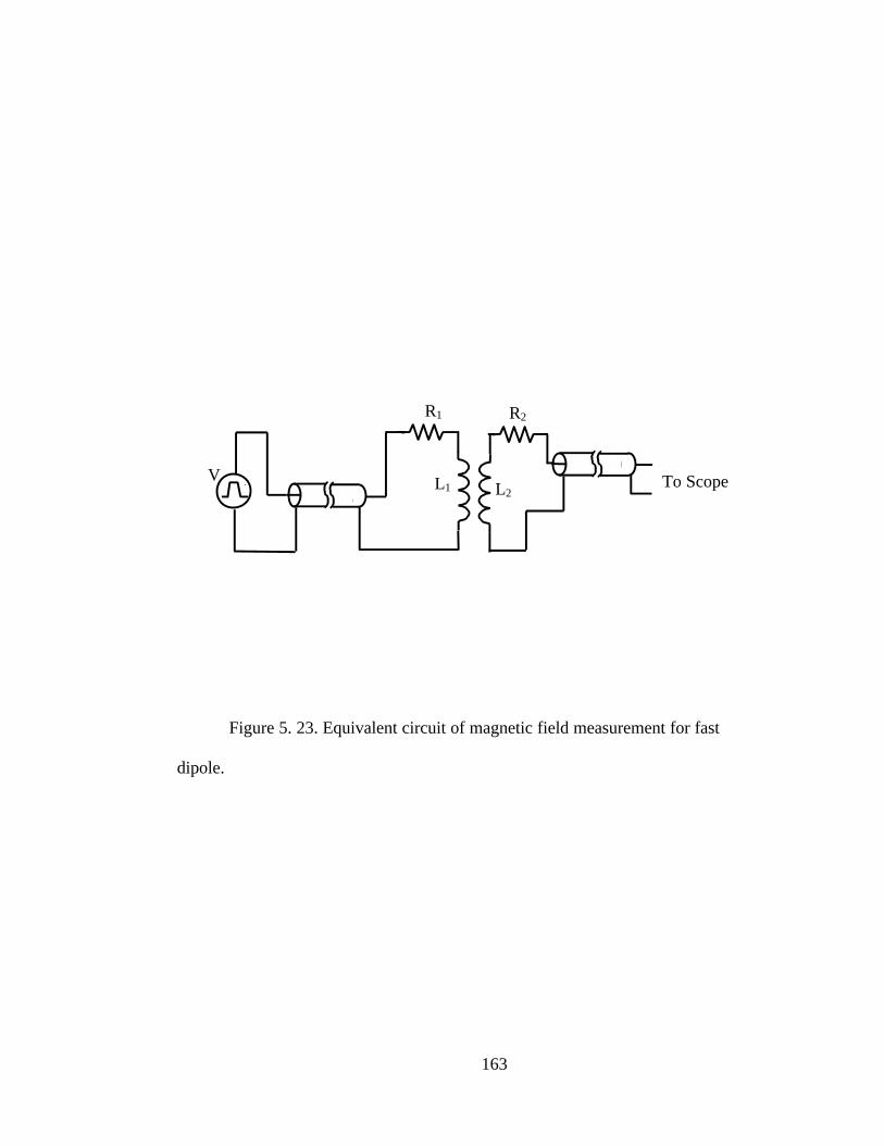
163
Figure 5. 23. Equivalent circuit of magnetic field measurement for fast
dipole.
L1 To ScopeV
R1
L2
R2
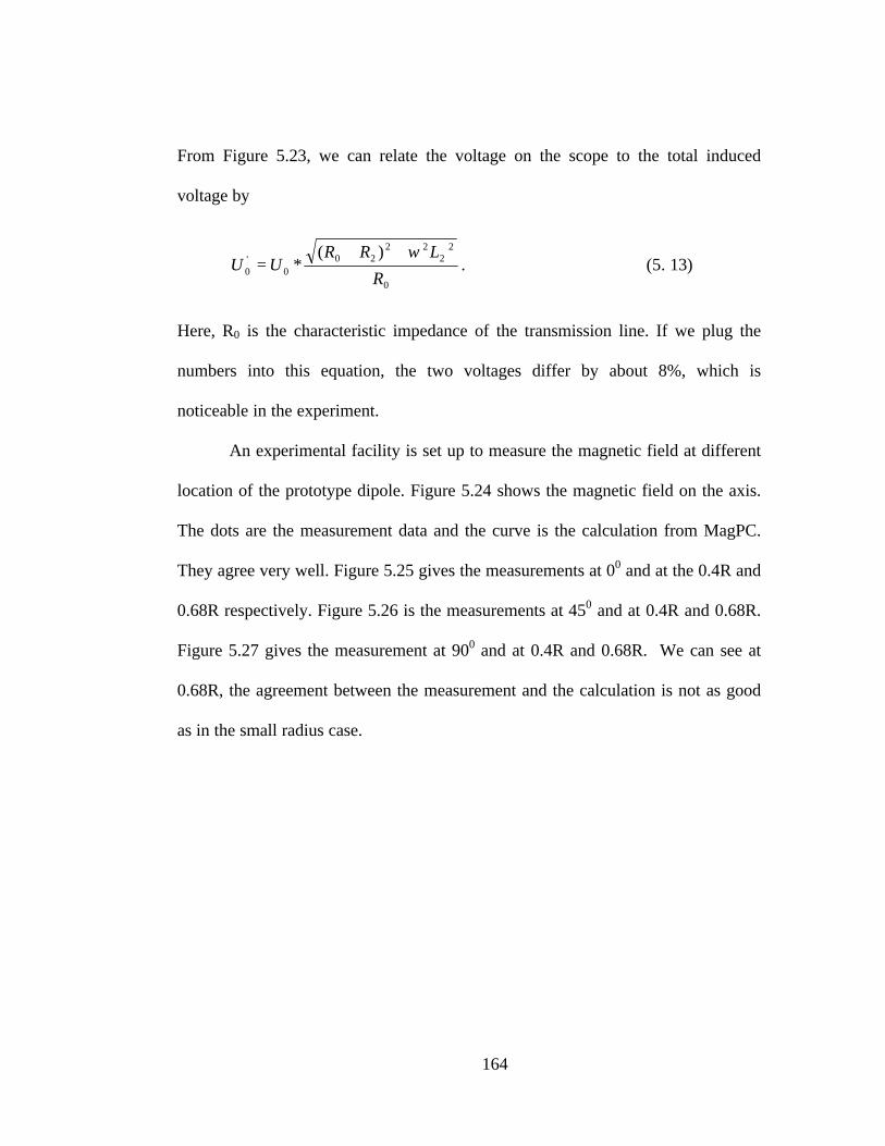
164
From Figure 5.23, we can relate the voltage on the scope to the total induced
voltage by
0
22
2220
0'0
)(*
R
LRRUU
ω++= . (5. 13)
Here, R0 is the characteristic impedance of the transmission line. If we plug the
numbers into this equation, the two voltages differ by about 8%, which is
noticeable in the experiment.
An experimental facility is set up to measure the magnetic field at different
location of the prototype dipole. Figure 5.24 shows the magnetic field on the axis.
The dots are the measurement data and the curve is the calculation from MagPC.
They agree very well. Figure 5.25 gives the measurements at 00 and at the 0.4R and
0.68R respectively. Figure 5.26 is the measurements at 450 and at 0.4R and 0.68R.
Figure 5.27 gives the measurement at 900 and at 0.4R and 0.68R. We can see at
0.68R, the agreement between the measurement and the calculation is not as good
as in the small radius case.

165
Figure 5. 24. Measurement and Mag-PC calculation of the vertical magnetic
field on axis.
-0.005
0
0.005
0.01
0.015
0.02
0.025
-0.2 -0.15 -0.1 -0.05 0 0.05 0.1 0.15 0.2
By(
Gau
ss)
Distance from the midplane (m)
Curve: theoretical calculationDots: measurement data
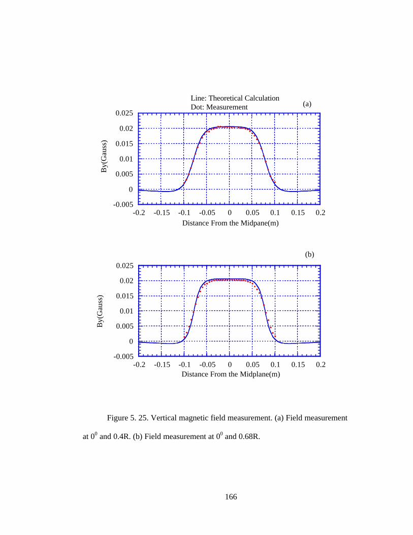
166
Figure 5. 25. Vertical magnetic field measurement. (a) Field measurement
at 00 and 0.4R. (b) Field measurement at 00 and 0.68R.
-0.005
0
0.005
0.01
0.015
0.02
0.025
-0.2 -0.15 -0.1 -0.05 0 0.05 0.1 0.15 0.2
By(
Gau
ss)
Distance From the Midpane(m)
Line: Theoretical CalculationDot: Measurement (a)
-0.005
0
0.005
0.01
0.015
0.02
0.025
-0.2 -0.15 -0.1 -0.05 0 0.05 0.1 0.15 0.2
By(
Gau
ss)
Distance From the Midplane(m)
(b)
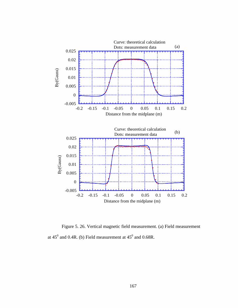
167
Figure 5. 26. Vertical magnetic field measurement. (a) Field measurement
at 450 and 0.4R. (b) Field measurement at 450 and 0.68R.
-0.005
0
0.005
0.01
0.015
0.02
0.025
-0.2 -0.15 -0.1 -0.05 0 0.05 0.1 0.15 0.2
By(
Gau
ss)
Distance from the midplane (m)
Curve: theoretical calculationDots: measurement data (a)
-0.005
0
0.005
0.01
0.015
0.02
0.025
-0.2 -0.15 -0.1 -0.05 0 0.05 0.1 0.15 0.2
By(
Gau
ss)
Distance from the midplane (m)
Curve: theoretical calculationDots: measurement data (b)

168
Figure 5. 27. Vertical magnetic field measurement. (a) Field measurement
at 900 and 0.4R. (b) Field measurement at 900 and 0.68R.
-0.005
0
0.005
0.01
0.015
0.02
0.025
-0.2 -0.15 -0.1 -0.05 0 0.05 0.1 0.15 0.2
By(
Gau
ss)
Distance from the midplane (m)
Curve: theoretical calculationDots: measurement data (a)
-0.005
0
0.005
0.01
0.015
0.02
0.025
-0.2 -0.15 -0.1 -0.05 0 0.05 0.1 0.15 0.2
By(
Gau
ss)
Distance from the midplane (m)
(b)
169
5.4 Summary
In this chapter, the overall design of the UMER was introduced and
discussed. The principle of capacitive BPM was studied and a prototype capacitive
BPM was designed and tested. The test result showed that our understanding of the
capacitive BPM is correct and the accuracy of the BPM is good enough to be used
in the UMER. Work has also been conducted to study a fast rise-time dipole. By
using the combination of parallel and series structure, we demonstrated that the
rise-time and the field profile of this kind of dipole could meet the requirements of
the UMER.
170
Chapter 6
Conclusion
Systematic and pioneering experimental work has been performed to study
the resistive-wall instability of space-charge waves in space-charge dominated
electron beam. In the linear regime, we were able to observe the propagation and
growth or decay of space-charge waves in the resistive environment. However, in
the nonlinear regime, we observed the abnormal increase of the fast wave
amplitude and the growth or decaying rate of the fast waves is amplitude
dependent. By doing the same experiments in the conducting wall, we
demonstrated that this abnormal phenomenon only occurs in the resistive pipe. So
far, there are no analytical theories or simulations that would predict this
phenomenon.
The energy spread measurement of the space-charge dominated beam is a
challenge and mystery in our lab. People always observed large energy spread from
the beam. In this thesis, it was demonstrated that this large energy spread is due to
the imperfection of the energy analyzer itself. As a consequence, a new structure of
the energy analyzer was designed. Both simulation and experimental test showed
that the new energy analyzer has much better resolution and can be used to
characterize the energy profile of electron beam with high resolution.
171
So far, all the experiments were performed on a linear transport system. The
short distance of the system limits a lot experiment work. UMER, which is being
designed and built at the University of Maryland, will offer a much better tool to
study and bench test the space-charge-dominated beam. Even if the beam only
propagate by several turns, it already has a much longer transport distance than the
linear system that we currently are using. To guarantee the success of the UMER,
we must be able to measure the beam position accurately and steer the beam back
to the orbit. A prototype capacitive BPM has been designed and bench tested. The
results showed that this kind of BPM has good enough time response and accuracy
for the UMER. A real BPM is being designed and will be tested.
At the junction of the injection line and the UMER main ring, we need a
fast rise-time dipole to steer the beam into the ring. Some work has been performed
to study a method to reduce the inductance, therefore, the rise-time, of this dipole.
The test of a prototype structure of this kind of dipole showed that it is possible to
reduce the inductance to the desired value by using a combination of parallel and
series structure. Of course, there is a lot of engineering work to do to design a real
fast dipole for the UMER.
For the future work, more experiments could be done to study the resistive-
wall instability. For example, the capacitive effect on the growth rate is a very
interesting topic. The experiments on the slow waves were limited due to the
cathode condition. With the new cathode, more work can be done to study the
172
amplitude related growth rate of the slow wave. In addition, the measurement of the
possible emittance growth due to resistive wall is also very interesting and
challenging. After the UMER is completed, we are also able to study the beam
instability due to the induction gap impedance in a much longer distance and more
valuable results could be obtained.
The newly designed energy analyzer will be a promising tool to study the
beam energy profile in different situations. For example, we are able to measure the
energy spread increase due to the Boersch effect and the longitudinal-longitudinal
relaxation effect etc.
After all, many achievements have been presented in the thesis. However,
more valuable and challenging work can be done in this area with facilities already
developed in our lab and with the completion of UMER.
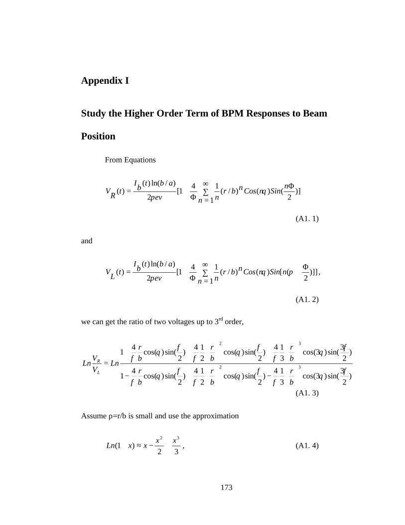
173
Appendix I
Study the Higher Order Term of BPM Responses to Beam
Position
From Equations
)]2
()1
()/(14
1[2
)/ln()()(
Φ∑∞
=Φ+=
nSin
nnCosnbr
nv
abtb
It
RV θ
πε
(A1. 1)
and
)]]2
([)1
()/(14
1[2
)/ln()()(
Φ+∑
∞
=Φ+= πθ
πεnSin
nnCosnbr
nv
abtb
It
LV ,
(A1. 2)
we can get the ratio of two voltages up to 3rd order,
)2
3sin()3cos(
3
14)
2sin()cos(
2
14)
2sin()cos(
41
)2
3sin()3cos(
3
14)
2sin()cos(
2
14)
2sin()cos(
41
32
32
φθ
φφ
θφ
φθ
φ
φθ
φφ
θφ
φθ
φ
−
+−
+
++
=
b
r
b
r
b
r
b
r
b
r
b
r
LnV
VLn
L
R
(A1. 3)
Assume ρ=r/b is small and use the approximation
32)1(
32 xxxxLn +−≈+ , (A1. 4)
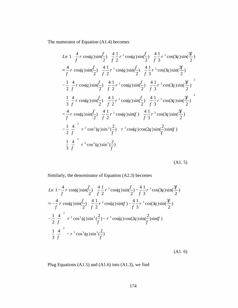
174
The numerator of Equation (A1.4) becomes
+
+
−
++=
+++
++−
++≈
+++
)2
(sin)(cos4
3
1
)sin()2
sin()2cos()cos()2
(sin)(cos4
2
1
)2
3sin()3cos(
3
14)sin()cos(
2
14)
2sin()cos(
4
)2
3sin()3cos(
3
14)
2sin()cos(
2
14)
2sin()cos(
4
3
1
)2
3sin()3cos(
3
14)
2sin()cos(
2
14)
2sin()cos(
4
2
1
)2
3sin()3cos(
3
14)
2sin()cos(
2
14)
2sin()cos(
4
)2
3sin()3cos(
3
14)
2sin()cos(
2
14)
2sin()cos(
41
333
3
3222
2
32
3
32
2
32
32
32
φθρ
φ
φφ
θθρφ
θρφ
φθρ
φφθρ
φφ
θρφ
φθρ
φφ
θρφ
φθρ
φ
φθρ
φφ
θρφ
φθρ
φ
φθρ
φφ
θρφ
φθρ
φ
φθρ
φφ
θρφ
φθρ
φLn
(A1. 5)
Similarly, the denominator of Equation (A2.3) becomes
−
+
−
−
−+−≈
−+−
)2
(sin)(cos4
3
1
)sin()2
sin()2cos()cos()2
(sin)(cos4
2
1
)2
3sin()3cos(
3
14)sin()cos(
2
14)
2sin()cos(
4
)2
3sin()3cos(
3
14)
2sin()cos(
2
14)
2sin()cos(
41
333
3
3222
2
32
32
φθρ
φ
φφ
θθρφ
θρφ
φθρ
φφθρ
φφ
θρφ
φθρ
φφ
θρφ
φθρ
φLn
(A1. 6)
Plug Equations (A1.5) and (A1.6) into (A1.3), we find

175
)(cos)
2(sin
3
128)2cos()cos(
)2
sin()sin(16
)2
3sin(
)3cos(3
8)cos(
)2
sin(8
333
3
32
3
θρφ
φ
θθρφ
φφ
φ
φ
θρθρφ
φ
+−
+=l
R
V
VLn
(A1. 7)
Using the relationships
bx /)cos( =θρ ,
( ) 3233 /3)3cos( bxyx −=θρ ,
( ) 3233 /)2cos()cos( bxyx −=θθρ , and
3333 /)(cos bx=θρ ,
Equation (A1.7) becomes
3
2
2
3
3
3
3
2
)2
sin()sin(16
)2
3sin(
8
)2
(sin
3
128)
2sin()sin(
16)
2
3sin(
3
8
10
20)
2sin(
10
160
ln10
2020
b
xy
b
x
Lnb
x
Ln
V
V
LnV
VLog
L
R
l
R
+−+
+−+=
=
φ
φφ
φ
φ
φ
φ
φ
φφ
φ
φ
φ
φ
(A1. 8)
This is Equation (5.7) in Chapter 5.
Note if we want the coupling term to vanish, we let
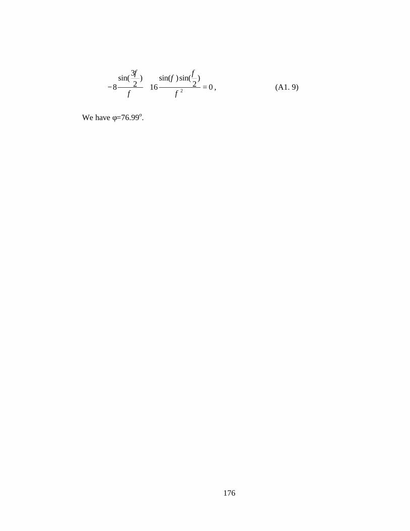
176
0)
2sin()sin(
16)
23
sin(8 2 =+−
φ
φφ
φ
φ
, (A1. 9)
We have φ=76.99o.
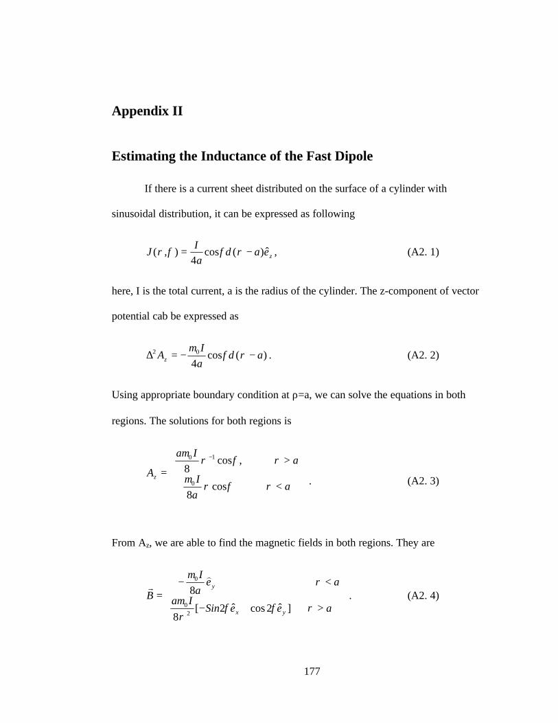
177
Appendix II
Estimating the Inductance of the Fast Dipole
If there is a current sheet distributed on the surface of a cylinder with
sinusoidal distribution, it can be expressed as following
zeaa
IJ ˆ)(cos
4),( −= ρφδφρ , (A2. 1)
here, I is the total current, a is the radius of the cylinder. The z-component of vector
potential cab be expressed as
)(cos4
02 aa
IAz −−=∆ ρφδ
µ. (A2. 2)
Using appropriate boundary condition at ρ=a, we can solve the equations in both
regions. The solutions for both regions is
<
>=
−
aa
I
aIa
Az
ρφρµ
ρφρµ
cos8
,cos8
0
10
. (A2. 3)
From Az, we are able to find the magnetic fields in both regions. They are
>+−
<−=
aeeSinIa
aea
I
B
yx
y
ρφφρµ
ρµ
]ˆ2cosˆ2[8
8
20
0 )r
. (A2. 4)
178
Associated the magnetic field, the energy in the space can also be found, it is
202
0 0
02
642)2/( IddBW
πµφρπρµ
π
== ∫ ∫∞
. (A2. 5)
The total energy is related to the inductance of the system by
202
1ILW = , (A2. 6)
here, L0 is the inductance per unit length of the system, and I is the current. From
this relation, we can find the inductance per unit length as
)/(1023.132
700 mHL −×==
πµ(A2. 7)
The dipole length D is 0.05 m, and if we connect the four quadrants in series, the
total inductance of the dipole is
)(1084.916 80 HDLL −×=×= (A2. 8)

179
References
[1] M. Reiser, Theory and Design of Charged Particle Beams (John Wiley & Sons,
Inc, New York, 1994).
[2] E. P. Lee, Nuovo Cimento, 106A (1993).
[3] T. C. Marshall, Free Electron Lasers (Macmillan Pub. Co., New York, 1985).
[4] D. Kehne, Ph.D. Dissertation, Department of Electrical Engineering,
University of Maryland, 1992.
[5] J. G. Wang, S. Bernal, P. Chin, et al., Nucl. Instr. & Meth. in Phys. Res.,
A(415) 422 (1998).
[6] J. G. Wang and M. Reiser, Phys. Plasmas, 5(5) (1998).
[7] H. Suk, Ph.D. Dissertation, Physics Department, University of Maryland at
College Park, 1996.
[8] C. K. Birdsall, G. R. Brewer, and A. V. Haeff, Proc. of The I.R.E., 41(7) 865
(1953).
[9] M. Sarstedt, P. Herz, W. B. Kunkel, et al. PAC, 1995, Dallas, Texas.
[10] V. V. Aleksandrov, N. S. Dikansky, N. C. Kot, et al., Phys. Rev. A, 46(10)
6628 (1992).
[11] D. Habs, J. Kramp, P. Krause, et al., Phys. Scr., T22 269 (1988).
[12] H. Poth, Phys. Rep., 196 (1990).

180
[13] J. G. Wang, E. Boggasch, P. Haldemann, et al., IEEE Tran. Elec. Dev., 37(12)
2622 (1990).
[14] J. G. Wang, D. X. Wang, and M. Reiser, Nucl. Instr. & Meth. in Phys. Res.,
A316 112 (1992).
[15] C. K. Birdsall and J. R. Whinnery, J. Appl. Phys., 24(3) 314 (1953).
[16] E. Lee. Proceedings of the 1981 Linear Accelerator Conference, Santa Fe,
NM, 1981.
[17] D. A. Callahan, A. B. Langdon, and A. Frideman, J. Appl. Phys., 81(8) 3398
(1997).
[18] J. G. Wang, Y. Zou, H. Suk, et al. PAC Conference, 1999, New York.
[19] H. Suk, J. G. Wang, Y. Zou, et al. PAC Conf., 1997, Vancouver.
[20] H. Suk, J. G. Wang, M. Reiser, et al., J. Appl. Phys., 86(3) 1699 (1999).
[21] J. G. Wang and M. Reiser, Phys. Fluids B, 5(7) 2286 (1993).
[22] J. G. Wang, H. Suk, and M. Reiser, Phys. Rev. Lett., 79(6) 1042 (1997).
[23] J. G. Wang, M. Reiser, W. M. Guo, et al., Pat. Accel., 37-38(181) (1992).
[24] J. G. Wang and M. Reiser. IEE Particle Accelerator Conference, 1991, San
Francisco, CA.
[25] D. C. Davidson, Theory of Nonneutral Plasmas (Addison-Wesley, Menlo
Park, CA, 1989).
[26] D. A. Callahan, Ph.D. Dissertation, University of California, DAvis, 1989.
181
[27] J. G. Wang, D. X. Wang, and M. Reiser, Phys. Rev. Lett., 71(12) 1836
(1993).
[28] J. G. Wang, D. X. Wang, H. Suk, et al., Phys. Rev. Lett., 74(16) 3153 (1995).
[29] V. I. Kudelainen, V. A. Lebedev, and I. N. Meshkov, Sov. Phys. JETP, 56(6)
1191 (1982).
[30] M. Reiser, P. G. O'Shea, R. A. Kishek, et al. PAC Conference, 1999, New
York.
[31] N. Brown, Ph.D. Dissertation, Physics Department, University of Maryland at
College Park, 1995.
[32] J. A. Simpson, Rev. Sci. Instr., 32(12) 1283 (1961).
[33] A. B. El-Kareh and M. A. Simither, Journal of applied Physics, 50(9) 5596
(1979).
[34] A. Faltens, E. P. Lee, and S. S. Rosenblum, J. Appl. Phys., 61(12) 5219
(1987).
[35] G. H. Jansen, Coulomb Interactions in Particle Beams (Academic Press,
INC., Boston, 1990).
[36] M. Reiser, S. Bernal, A. Dragt, et al., Fus. Eng. Des., 00 (1996).
[37] T. J. Fessenden, B. W. Stallard, and G. G. Berg, Rev. Sci. Instr., 43(12) 1789
(1972).
[38] H. Suk, J. G. Wang, S. Bernal, et al. PAC, 1997, Vancouver, Canada.
182
[39] F. J. Deadrick, J. J. Barnard, T. J. Fessenden, et al. PAC, 1995, Dallas, TX.
[40] T. F. Godlove, S. Bernal, and M. Reiser. PAC, 1995.
[41] A. Friedman, D. P. Grote, and I. Haber, Phys. Fluids, B 4(7) 2203 (1992).
[42] I. Haber, D. A. Callahan, A. Friedman, et al. 1995 Particle Accelerator
Conference and International Conference on High-Energy Accelerators, 1995,
Dallas, Texas.
[43] Y. Zou, J.G. Wang, H. Suk, M. Reiser, Accepted for publication at Phys. Rev.
Lett., May 2000.
[44] C.D. Child, Phys. Rev. Ser. I 32, 492 (1911).
[45] I. Langmuir, Phys. Rev. Ser. II, 2, 450 (1913).