Embed Size (px)
Citation preview

JSPS-EPSRC-DFG Core-to-Core Programme
York-Tohoku-Kaiserslautern Research Symposium on
“New-Concept Spintronics Devices”
Abstracts
12-14 June 2019
Departments of Physics and Electronic Engineering University of York

– 1 –
FML '( : V CP ') : V 6Z ' : V.0)& 2Z IV 6 T WV.0) M V 7ZILa.0 & 2 ZSIZL 8 TTMJZIVL.0 I IN U BP ZI.0 &/0&&/0'&/0(&/0)&/0 &/0 &
'&0&& BI T CMVLTMZ DV WN GWZS'&0'& 8 LMW PVW CWPWS DV'&0(& WJ W DMVW :B B WVLWV'&0)& :WPV 8IVL 5 BA3'&0 &'&0 &''0&&''0'&''0(&''0)&''0 &''0 &'(0&&'(0'&'(0(&'(0)&'(0 &'(0 &')0&&')0'&')0(&')0)&')0 &')0 &' 0&&' 0'&' 0(&' 0)&' 0 &' 0 &' 0&&' 0'&' 0(&' 0)&' 0 &' 0 &' 0&&' 0'&' 0(&' 0)&' 0 &' 0 &'-0&&'-0'&'-0(&'-0)&'-0 &'-0 &
B V3ITWZ ZWV KIVL
IV TI WV
MV VO
B V ZWV K: VK WV
IOVM KBSaZU WV
5 IVOMTW I I WIVVWCD I MZ TI MZV
PW WOZI P
I IN U BP ZICWPWS DV
M P K MVVIDV WN GWZS
3WNNMM CMI 2ZMIS
VKP IVL W MZ
3WNNMM CMI 2ZMIS
VKP IVL W MZ
BP OMU b SIUCWPWS DV
5 R BI WPCWPWS DV DV WN
CWSaW
:B BZM MV I WV
1 IU I U ZI:B B WVLWV
1VNMZZWUIOVM KB V ZWV K
8M TMZ 1TTWa4M KM
B V CWZY M4M KM
B M PMV KE MDV WN 7TI OW
E VKMV 2IT bB V MK
1 MT 8WNNUIVV1ZOWVVM I T IJ
GW P VWJ ISI IVDV WN 5TMK ZW 3WUU V
BIU S 4 I7 ICWPWS DV
AWJMZ 3IZ MV MZUMK
CISIP LM JW ICWPWS DV
3PIWT IVO HPIVOCWPWS DV
I IP W C R SI ICWPWS DV
: V TIVLZWCWPWS DV
D3MZMUWVa
7eV MZ AMDV WN 2 MTMNMTL
:W 2IZSMZDV WN MML
:WPIV B MZUMK
3PZ W PMZ IZZWDV WN MML
1 ZM 6MZZM ZIDV WN GWZS
: V IS ICWPWS DV
(4 B V4M KM IVLCW WTWO KIT5NNMK
7MWZO WV 6ZMaUIVVCD I MZ TI MZV
8 ZWIS B SMOI I9 B
3WNNMM CMI 2ZMIS 3WNNMM CMI 2ZMIS
B V AIVLWU1KKM
MUWZa
JWZ BUMRSIT3bMKP 1KIL WN BK
8 LMW PVWCWPWS DV
2MZVIZL 4 dVaB V MK
1VLZM MVM GWZS DV
2 ZSIZL 8 TTMJZIVLCD I MZ TI MZV
CIS aI BI WPCWSaW 9V WN CMKPI P I Tc
:7 DV WN I Vb
IOVWV KIVL B V4aVIU K
FM KPIW GCWPWS DV
1 N U 8 ZWPI IDV WN GWZS
I MZ IT4M MTW UMVNWZ B V ZWV K4M KM
CPWUI CPWU WVDV WN IVKPM MZ
3WNNMM CMI 2ZMIS
1VLZM ZIDV WN GWZS
WS CISIVI PCWPWS DV
IZS M VIZDV WN 2 MTMNMTL
S P SW WOIVMCWPWS DV

– 2 –
Wednesday, 12 June
07:45 Bus departure from Holiday Inn York City Centre
08:00 Bus departure from York Pavilion Hotel
08:15 Registration Entrance, Exhibition Centre
08:30 Opening Chair: Atsufumi Hirohata (P/X 001)
08:30~08:35 Brian Fulton (Dean of Science, Univ. of York)
08.35~08.40 Kevin O’Grady (UK PI, Univ. of York)
08:40~08:45 Burkard Hillebrands (German PI, Technical Univ. of Kaiserslautern)
08:45~08.50 Masafumi Shirai (Japanese PI, Tohoku Univ.)
08:50 Spintronic Junctions Chair: Atsufumi Hirohata (P/X 001)
08:50~09:20 Masafumi Shirai (Tohoku Univ.), “Computational mining of quaternary
Heusler alloys possessing high spin polarization and high Curie temperature”
09:20~09:50 Günter Reiss (Univ. of Bielefeld), “Thermal properties of magnetic tunnel
junctions”
09:50~10:20 Keith McKenna (Univ. of York), “Structure and properties of extended defects
in spintronic materials through first principles calculations and electron microscopy”
10:20~10:50 Vincent Baltz (Spintec), “Different aspects around the topic of
antiferromagnetic spintronics”
10:50 Coffee/Tea Break (P/T 005)
11:10 Magnonics and Spin Dynamics Chair: Evangelos Papaioannou (P/X 001)
11:10~11:40 Burkard Hillebrands (Technical Univ. of Kaiserslautern), “Magnonics with
macroscopic quantum states”
11:40~12:10 Yoshinobu Nakatani (Univ. of Electro-Commun.), “Reducing the switching
current with an antiferromagnetic coupling structure in nanomagnets with perpendicular
anisotropy”
12:10~12:40 Georg von Freymann (Technical Univ. of Kaiserslautern), “Light induced optics
for spin-waves”
12:40 Lunch and Poster (P/T 005)
14:00 Spin Caloritronics and Manipulation Chair: Hiroaki Sukegawa (P/X 001)
14:00~14:30 Eiji Saitoh (Tohoku Univ. & Univ. of Tokyo), “Spin current in quantum spin
liquids and superconductions”
14:30~15:00 Matthias Kläui (Johannes Gutenberg Univ. of Mainz), “Topological spin
dynamics in ferro- and antiferromagnets”
15:00~15:20 Joseph Barker (Univ. of Leeds), “Quantum thermodynamics of yttrium iron
garnet”
15:20~15:40 Evangelos Papaioannou (Technical Univ. of Kaiserslautern), “Revealing the

– 3 –
coupling mechanism of plasmonic and magneto-optically induced near-fields in
Bi:YIG/Au nanostructures”
15:40 Coffee/Tea Break (P/T 005)
16:00 Spin Random Access Memory Chair: Keith McKenna (P/X 001)
16:00~16:30 Hideo Ohno (Tohoku Univ.), “Spintronics nanodevice – From integrated circuit
application to mimicking brain function –”
16:30~17:00 Bernard Diény (Spintec), “Perpendicular shape anisotropy STT-MRAM: A
route towards sub-10nm STT-MRAM scaling”
17:00~17:30 Andrew Kent (New York Univ.), “Spin-transfer switching and magnetic
interactions in perpendicular magnetic tunnel junctions nanopillars”
17:30~18:00 Johan Swerts (imec), “Material and integration challenges of magnetic tunnel
junctions in advanced spintronic applications”
18:10 Bus departure from the University
18:20 Bus arrival at York Pavilion Hotel
18:30 Bus arrival and departure from Holiday Inn York City Centre
18:40 Bus departure from the University Library for those staying at the Franklin House
18:50 Bus departure from York Pavilion Hotel
19:15 Bus arrival at St Vincent Arms
19:15 Dinner (invited guests only) St Vincent Arms
22:00 Departure from St Vincent Arms
22:25 Arrival at York Pavilion Hotel
22:35 Arrival at the University Library for those staying at the Franklin House
22:45 Arrival at Holiday Inn York City Centre

– 4 –
Thursday, 13 June
08:15 Bus departure from Holiday Inn York City Centre
08:30 Bus departure from York Pavilion Hotel
08:45 Registration Entrance, Exhibition Centre
09:00 Magnetic Skyrmions Chair: Gonzalo Vallejo-Fernandez (P/X 001)
09:00~09:30 Axel Hoffmann (Argonne Nat’l Lab.), “Spin current generation, detection, and
transport with antiferromagnets”
09:30~10:00 Stephen McVitie (Univ. of Glasgow), “Lorentz microscopy study of hybrid
walls and skyrmion nucleation in multilayer materials”
10:00 MOU Ceremony Chair: Kevin O’Grady (P/X 001)
10:00~10:10 Saul Tendler (Acting Vice-Chancellor, Univ. of York)
10:10~10:20 Hideo Ohno (President, Tohoku Univ.)
10:20~10:30 Nobuo Ueno (Director, JSPS London)
10:30~10:40 John Hand (Lead of Physical Sciences, EPSRC)
10:40 Photograph (Entrance)
10:50 Coffee/Tea Break (P/T 005)
11:10 Material Development for Spintronic Devices Chair: Takahide Kubota (P/X 001)
11:10~11:40 Koki Takanashi (Tohoku Univ.), “Spin-caloritronics in ordered-alloy thin films”
11:40~12:10 Atsufumi Hirohata (Univ. of York), “Spintronic devices: From materials
development to characterisation”
12:10~12:30 Hiroaki Sukegawa (NIMS), “Significant TMR oscillation effect in magnetic
tunnel junctions with a MgAl2O4 barrier”
12:30~12:50 Andrew Pratt (Univ. of York), “Effect of surface anisotropy on magnetic
domain formation at the surface of Fe3O4(001)”
12:50 Lunch and Poster (P/T 005)
14:00 JSPS Presentation Chair: Masafumi Shirai (P/X 001)
14:00~14:20 Asami Matsumura (JSPS London)
14:20 Antiferromagnetic Spintronics Chair: Masafumi Shirai (P/X 001)
14:20~14:50 Takuya Satoh (Tokyo Inst. of Technol.), “Magnon and phonon-polariton
excitations in multiferroic BiFeO3”
14:50~15:20 Libor Šmejkal (Czech Acad. of Sci.), “Topological antiferromagnetic spintronics:
crystal Hall antiferromagnets”
15:20~15:40 Weichao Yu (Tohoku Univ.), “A theoretical proposal of an in-memory spin-
wave logic gate for all Boolean operations”
15:40 Coffee/Tea Break (P/T 005)
16:00 2D Spin Devices and Topological Effects Chair: Shigemi Mizukami (P/X 001)

– 5 –
16:00~16:30 Junsaku Nitta (Tohoku Univ.), “Topological Transition in Rashba Spin
Interferometers”
16:30~17:00 Aires Ferreira (Univ. of York), “Gate-tunable charge-to-spin interconversion in
atomically-thin van der Waals heterostructures at room temperature”
17:00~17:20 Justin Llandro (Tohoku Univ.), “Size dependence of the influence of edge effects
in nanoscale perpendicular-anisotropy magnetic tunnel junctions”
17:20~17:50 Christopher Marrows (Univ. of Leeds), “Skyrmions in chiral magnetic
multilayers”
18:00 Bus departure from the University
18:10 Bus arrival at York Pavilion Hotel
18:20 Bus arrival and departure from Holiday Inn York City Centre
18:30 Bus departure from the University Library for those staying at the Franklin House
18:40 Bus departure from York Pavilion Hotel
1900 Bus arrival at Loch Fyne
19:00 Dinner (invited guests only) Loch Fyne
22:00 Departure from Loch Fyne
22:15 Arrival at the University Library for those staying at the Franklin House
22:25 Arrival at York Pavilion Hotel

– 6 –
Friday, 14 June
08:15 Bus departure from Holiday Inn York City Centre
08:30 Bus departure from York Pavilion Hotel
09:00 Heusler-Alloy Devices Chair: Mikihiko Oogane (P/X 001)
09:00~09:30 Shigemi Mizukami (Tohoku Univ.), “Magnetic tunnel junction with a
manganese nano-layer”
09:30~09:50 Robert Carpenter (imec), “Enabling BEOL compatibility in top-pinned STT-
MRAM”
09:50~10:10 Takahide Kubota (Tohoku Univ.), “Mn-based perpendicularly magnetized
films with Cu2Sb-type crystal structure”
10:10~10:40 Markus Meinart (Univ. of Bielefeld), “Ultra-low switching current density in
all-amorphous W-Hf/CoFeB/TaOx film stacks with perpendicular magnetic anisotropy”
10:40~11:00 Masahito Tsujikawa (Tohoku Univ.), “Voltage-controlled magnetic anisotropy
on Ir doped Co-based Heusler alloys”
11:00 Coffee/Tea Break (P/T 005)
11:30 Spin-Torque Devices Chair: Andrew Pratt (P/X 001)
11:30~12:00 Thomas Thomson (Univ. of Manchester), “Temperature-dependent studies of
coupled Fe55Pt45/Fe49Rh51 thin films and patterned elements”
12:00~12:20 Samik DuttaGupta (Tohoku Univ.), “Spin Hall magnetoresistance in
antiferromagnet/nonmagnet metallic structures”
12:20~12:40 Chaoliang Zhang (Tohoku Univ.), “Efficient control of magnetization utilizing
spin-orbit torque and spin-transfer torque”
12:40~13:10 Mikihiko Oogane (Tohoku Univ.), “Development high-sensitive magnetic
tunnel junction based sensors”
13:15 Bus departure from the University
13:25 Bus arrival at York Railway Station

– 7 –
Abstracts of Oral Presentations

– 8 –
Computational mining of quaternary Heusler alloys possessing high spin polarization and high Curie temperature
Masafumi Shirai1, 2, 3
1. Research Institute of Electrical Communication (RIEC), Tohoku University 2. Center for Spintronics Research Network (CSRN), Tohoku University
3. Center for Science and Innovation of Spintronics (CSIS), Tohoku University Half-metallic Heusler alloys have been studied extensively for application to electrode materials of
magnetic tunnel junctions (MTJ). The inevitable obstacle of the MTJ using Heusler alloys is considerable reduction of magnetoresistance (MR) with increasing temperature. In order to predict promising materials which overcome the obstacle, we carried out comprehensive exploration of quaternary Heusler alloys possessing high spin polarization and high Curie temperature by using ab initio density-functional calculation with the aid of machine learning.
We constructed a database which stores the physical quantities, e.g. equilibrium lattice constants, total energy, magnetization, spin polarization, Curie temperature and so on, evaluated by ab initio calculation for randomly selected 4,434 quaternary Heusler alloys. Then, we developed a predictor based on Random Forest [1] to predict the stability and the Curie temperature of quaternary Heusler alloys. We examined the feasibility of the predictor and confirmed relatively high precision; i.e. the accuracy for classification prediction of the stability reaches 87% and the correlation coefficient between predicted and ab initio values of the Curie temperature becomes greater than 0.76. The predictor revealed about 500 candidates which are stable and possess the Curie temperature higher than 800 K from among 96,768 sorts of quaternary Heusler alloys. We performed ab initio calculations for the candidates including for verification and successfully predicted about 20 sorts of half-metallic Heusler alloys which had not been reported so far.
In conclusion, we demonstrated that the machine learning is quite useful for efficient screening of materials possessing desirable properties.
This work was accomplished in collaboration with T. Kanemura, T. Roy, and M. Tsujikawa, and was partly supported by JST CREST (JPMJCR17J5), JSPS Core-to-Core program “New-Concept Spintronics Devices” and CSRN, Tohoku University. [1] W. S. Noble, Nat. Biotech. 24, 1565 (2006).
Session 1: Spintronic Junctions Chair: Atsufumi Hirohata 08:50~10:50 (P/X 001)

– 9 –
Thermal properties of magnetic tunnel junctions
G Reiss University of Bielefeld
Two types of responses of magnetic tunnel junctions (MTJs) to temperature will be discussed: A thermal gradient across the tunneling barrier generates a spin-dependent Seebeck voltage know
as Tunneling Magneto Seebeck (TMS) effect. The amplitude of both the Seebeck background voltage Vs as well as of the TMS, however, have been limited to small values for conventional CoFeB electrodes. For Heusler compounds with a band edge of one spin species close to the Fermi level, however, we demonstrate both large values of Vs and the TMS in agreement with arguments based on the band structure of the material.
For CoFeB based magnetically perpendicular MTJs, a thermally activated superparamagnetic (sp) behaviour can be found that is caused most probably by a granular character of the very thin CoFeB electrodes. We discuss entropic and energetic influences on the sp-switching rates and demonstrate their dependence on magnetic and electric fields as external input parameters. The results allow to realize tuning curves for networks of sp-MTJs that can mimic noisy neural-like networks with large redundancy.

– 10 –
Structure and properties of extended defects in spintronic materials through first principles calculations and electron microscopy
Keith McKenna
Department of Physics, University of York Extended defects such as grain boundaries, heterointerfaces and surfaces are ubiquitous in real
materials and spintronic devices. Often extended defects are deliberately introduced to realise particular functionalities (for example to inject spin polarized currents across an interface). In many other cases they are present simply as a result of growth technique employed or the device architecture. In either case a proper understanding of the structure, magnetic, electronic and spin transport properties of extended defects is essential to realise high performance. In this talk, I will present some of our recent work combining predictive first principles modelling with experimental transmission electron microscopy to unravel the structure and properties of extended defects with relevance to applications in spintronics and magnetism. These include MgO grain boundaries and dislocations with relevance to magnetoresistive tunnel junctions [1-5] and antiphase boundary defects in pure and Zn-doped iron oxides [6-8]. [1] Z-C. Wang et al, Nature 479, 380-383 (2011) [2] Z-C. Wang et al, Nature Communications 5, 3239 (2014) [3] Z-C. Wang et al, Nano Letters 16, 1530 (2016) [4] J. J. Bean et al, Scientific Reports 7, 45594 (2017) [5] J. J. Bean and K. P. McKenna, Physical Review Materials 2, 125002 (2018) [6] K. P. McKenna et al, Nature Communications 5, 5740 (2014) [7] D. Gilks et al, Scientific Reports 6, 20943 (2016) [8] N. Fontaina-Troitino et al, Journal of Materials Chemistry C 6, 12800 (2018)
– 11 –
Different aspects around the topic of antiferromagnetic spintronics
O. Gladii, R. L. Seeger, L. Frangou, G. Forestier, A. Hallal, P. Noël, S. Auffret, M. Rubio-Roy, I. Joumard, L. Vila, M. Chshiev, C. Gomez,
S. Gambarelli, M. Houzet, and V. Baltz Univ. Grenoble Alpes, CNRS, CEA, Grenoble INP
SPINTEC – CIME Nanotech – SYMMES – PHELIQS [email protected]
The paradigm shift consisting of using the spin-dependent properties of antiferromagnets in
electronics led to many exciting challenges around this topic.1,2 In this talk, we will first discuss experimental results about the use of spin pumping as a generic
probe to identify spin fluctuations and explore the physics of phase transitions. By selecting representative materials as spin-sinks - ferromagnetic and antiferromagnetic orders, metallic and insulating electrical states - and by choosing specific interacting environments to promote either electronic or magnonic transport, the results show that the phenomenon applies with all kinds of ordering and electrical states and all kinds of spin current.3-6
In search for spin fluctuations in several spin-sinks, we will also discuss how we found experimental evidence of self-induced spin Hall effect, corroborating the results of first-principle calculations.7,8
Beyond spin currents, we will finally present a stimulating example of how antiferromagnets and superconductors may envision a common future by showing how to infer essential information about domain walls using Cooper pairs through antiferromagnets.9,10 1 T. Jungwirth et al, Nat. Nanotechnol. 11, 231 (2016). 2 V. Baltz et al, Rev. Mod. Phys. 90, 015005 (2018). 3 Y. Ohnuma et al, Phys. Rev. B 89, 174417 (2014). 4 L. Frangou et al, Phys. Rev. Lett. 116, 077203 (2016). 5 Z. Qiu et al, Nat. Commun. 7, 12670 (2016). 6 O. Gladii et al, Phys. Rev. B 98, 094422 (2018) ; Appl. Phys. Express 12, 023001 (2019). 7 A. Tsukahara et al, Phys. Rev. B 89, 235317 (2014). 8 O. Gladii et al, to be published. 9 A. I. Buzdin, Rev. Mod. Phys. 77, 935 (2005). 10 R. L. Seeger et al, to be published.

– 12 –
Magnonics with macroscopic quantum states
Burkard Hillebrands Fachbereich Physik and Landesforschungszentrum OPTIMAS,
Technische Universität Kaiserslautern, 67663 Kaiserslautern, Germany With the fast growth in the volume of information being processed, researchers are charged with
the primary task of finding new ways for fast and efficient processing and transfer of data. Spin excitations—spin waves and their quanta magnons—open up a very promising branch of high-speed and low-power information processing.
Magnons are bosons, and thus they are able to form spontaneously a spatially extended, coherent macroscopic quantum state—magnon Bose-Einstein condensates (BEC), which can be established independently of the magnon excitation mechanism even at room temperature. An extraordinary challenge is the use of macroscopic quantum phenomena such as the magnon BEC for the information transfer and processing.
The information transfer can be realized by means of magnon supercurrents, which constitute the transport of angular momentum, driven by a phase gradient in the magnon-condensate wave function. Recently we have succeeded to create such a supercurrent by introducing a time-dependent spatial phase gradient into the wave function of a magnon BEC [1]. The temporal evolution of the BEC formed in a parametrically populated magnon gas was studied by means of time-, frequency-, and wavevector-resolved Brillouin light scattering spectroscopy in room-temperature YIG films. It has been found that local heating in the focal point of a probing laser beam leads to the excessive decay of the freely evolving BEC, which is a fingerprint of the supercurrent efflux of condensed magnons.
Here, I will also present the observation of a macroscopic BEC transport mechanism related to another type of motion of quantum condensates—second sound [2]. The condensed magnons being pushed out from the potential well within the heated area form compact density humps, which propagate through the thermally homogeneous film areas many hundreds of micrometers and reflect from sample edges. We refer to them as a superposition of Bogoliubov waves with oscillations of both the amplitude and the phase of the magnon BEC’s wave function. In the long-wavelength limit, realized in our experiment, these waves have a linear dispersion law and, thus, can be considered as a magnon second sound potentially featuring viscosity-free propagation.
The discovery of the long-distance macroscopic magnonic quantum state transport further advances the frontier of the physics of quasiparticles and allows for the application of related transport phenomena for low-loss data transfer in perspective magnon spintronics devices.
Financial support within the ERC Advanced Grant 694709 SuperMagnonics – ‘Supercurrents of Magnon Condensates for Advanced Magnonics’ is gratefully acknowledged.
[1] D. A. Bozhko, A. A. Serga, P. Clausen, V. I. Vasyuchka, F. Heussner, G. A. Melkov, A. Pomyalov,
V. S. L’vov, B. Hillebrands, Supercurrent in a room temperature Bose-Einstein magnon condensate, Nat. Phys. 12, 1057 (2016).
[2] D. A. Bozhko, A. J. E. Kreil, H. Yu. Musiienko-Shmarova, A. A. Serga, A. Pomyalov, V. S. L’vov, B. Hillebrands, Bogoliubov waves and distant supercurrent transport of magnon condensate at room temperature, Nat. Comm., submitted.
Session 2: Magnonics and Spin Dynamics Chair: Evangelos Papaioannou 11:10~12:40 (P/X 001)

– 13 –
Reducing the switching current with an antiferromagnetic coupling structure in nanomagnets with perpendicular anisotropy
Keisuke Kubota1, Keisuke Yamada2, Yoshinobu Nakatani1 1Graduate School of Informatics and Engineering, The University of Electro-Communications
2Faculty of Engineering, Gifu University
Reducing the switching current keeping the thermal stability is the key issue to realize STT-MRAM. As a method of reducing switching current while maintaining thermal stability, an ECC structure has been proposed [1-2]. In this study, an antiferromagnetic coupled structure (AFC) was proposed and the switching current was investigated by the simulation.
Figure 1 shows the MTJ structures used in this study. AFC consists of antiferromagnetically coupled a hard and soft layers [3]. SL is the conventional single layer structure to compared with the switching current (Fig. 1 (a)). In AFC, the thicknesses of the hard layer was 2 nm, and the thickness of the soft layer (hs) was varied from 0.5 to 1.5nm. The thickness of SL was 2nm. The diameters of AFC and SL were 30nm. The material parameters used in the simulation were a saturation magnetization Ms = 600 emu/cm3, a gyromagnetic ratio γ = 17.6 Mrad/(s・Oe), an exchange stiffness constant AIL = 1.6 μerg/cm, an inter layer exchange coupling AIL = -1.6 μerg/cm, the Gilbert damping constant α = 0.001~0.03. The thermal stability factor (Δ) changes by the perpendicular anisotropy constant (Ku) and thickness. We investigated the anisotropy constant to keep the thermal stability factor of Δ = 60 [3] by simulations. The anisotropy of SL was Ku
SL = 3.48 Merg/cm3. The anisotropy of the soft layer of AFC was KuAFC
s = 0 erg/cm3. The anisotropy of the hard layer of AFC for 0.5, 1.0, and 1.5 nm of hs were Ku
AFC = 4.20, 4.82, and 5.36 Merg/cm3, respectively. The pulse width of the spin current (tp) was 1.0 ns. A macrospin model was used in the simulation. Magnetization motion was calculated using the Landau-Lifshitaz-Gilbert equation with a spin-transfer term.
Figure 2 shows the effect of the thickness of the soft layer and the Gilbert damping constant on the switching current density. The swtiching current of AFC is larger than that of SL for largeα, however it is smaller than that of SL for small α. When α = 0.001, the switching current of AFC decreases as hs is increased. The reduction rate of the switching current with hs = 1.5 nm was 67% compared with SL.
References [1] H. Yoda, et al., “The Pursuit of Saving Energy Consumption of Memory Systems by MRAMs, from STT-MRAM to Voltage-Control Spintronics Memory (VoCSM).” Digests of Magnetics Conference (INTERMAG), 2018 IEEE International (2018). [2] K. Machida, et al., “Numerical study on a novel Curie temperature controlled hybrid thermo-magnetic structure for magnetic random access” Digests of Magnetics Conference (INTERMAG), 2017 IEEE International (2017). [3] K.Yamada et al., Appl. Phys. Lett. 106, 042402 (2015).

– 14 –
Light induced optics for spin-waves
Georg von Freymann1,2 1Physics Department and Research Center OPTIMAS, Technische Universität Kaiserslautern TUK,
67663 Kaiserslautern, Germany 2Fraunhofer Institute for Industrial Mathematics ITWM, 67663 Kaiserslautern, Germany
Guiding spin-waves in in-plane magnetized films is challenging due to the anisotropic dispersion
relations. We evaluate different optical elements, e.g. graded-refractive-index lenses, axicons, diffraction gratings, to understand how far analogies from conventional optics hold for the different spin-wave dispersions in YIG thin films. Combining several optical elements allows for creating a hardware Fourier-transformation (see Fig. 1), perhaps useful for redistributing spin-waves into different channels.
All optical elements can be realized in a reprogrammable fashion using light induced magnetization landscapes [1,2]. Even analogies to discrete optics can be realized in spin-wave systems, demonstrating the power of wave-based concepts.
Figure 1: (a) Spin wave GRIN lens. (b) Functionality of GRIN lases for different SW modes in a range of temperature differences. (c) GRIN lens-based SW Fourier optical system.
[1] Optically-Reconfigurable Magnetic Materials M. Vogel, A. V. Chumak, E. H. Waller, T. Langner, V. I. Vasyuchka, B. Hillebrands, and G. von Freymann Nat. Phys. 11, 487 (2015); https://dx.doi.org/10.1038/nphys3325
[2] Control of spin-wave propagation using magnetisation gradients M. Vogel, R. Aßmann, P. Pirro, A.V. Chumak, B. Hillebrands, G. von Freymann Scientific Reports 8, 11099 (2018); https://doi.org/10.1038/s41598-018-29191-2

– 15 –
Spin current in quantum spin liquids and superconductions
Eiji Saitoh1-5 1 ERATO-SQR, JST, Japan
2 Department of Applied Physics, The University of Tokyo, Japan 3 WPI-AIMR, Tohoku University, Japan
4 IMR, Tohoku University, Japan 5 ASRC, JAEA, Japan
Various types of spin current has been found in condensed matter. Such currents give rise to
various functions of matter, and they have led the recent progress of spintronics physics. The firstly discovered spin current is so called conduction-electron spin current, detected in terms
of the inverse spin Hall effect [1]. Secondly, we found spin-wave spin current in ferrimagnetic materials, in which spin waves carry angular momentum when their population is antisymmetric in the momentum space. Spin-wave spin current can also be created by heat current, which we named the spin Seebek effect. The concept of spin-wave spin current was expanded to other magnetically ordered phases such as antiferromagnets. Thirdly, we recently found that spin current can also be carried by spinons [2]; excitation from quantum spin liquid states.
In my talk, I will give an introduction to spin-wave spin current phenomena in antiferromagnets [3,4] with a well-defined Neel vector, spinon-spin injection into 1D quantum spin liquids, spin induced phenomena in antiferromagnets with DM interaction, and some related spin-current effects in antiferromagnets. This work was done with Dr. D. Hou, Dr. Z. Qiu, Dr. D. Hirobe, Dr. T. Kikkawa, Dr. K. Shiomi, Dr. K. Yamamoto, Prof. Y. Tserkovnyak, Prof. O. Gomonay, and Prof. G.E.W. Bauer.
[1] E. Saitoh et al. "Conversion of spin current into charge current at room temperature: inverse soin-Hall effect" Appl.Phys. Let. 88 (2006) 182509. [2] D. Hirobe, E. Saitoh et al. “One-dimensional spinon spin currents” Nature Phys. 13(2017)20. [3] Z. Qiu, E. Saitoh et al.“Spin-current probe for phase transition in an Insulators” Nature Com. 7 (2016) 12670. [4] Z Qiu, E Saitoh et al. “Spin colossal magnetoresistance in an antiferromagnetic insulator” Nature Mat. (2018).
Session 3: Spin Caloritronics and Manipulation Chair: Hiroaki Sukegawa 14:00~15:40 (P/X 001)

– 16 –
Topological Spin Dynamics in ferro- and antiferromagnets
Mathias Kläui1,2* 1Institute of Physics, Johannes Gutenberg University Mainz, 55099 Mainz, Germany
2Materials Science in Mainz, Staudinger Weg 9, 55128 Mainz, Germany In our information-everywhere society IT is a major player for energy consumption. Novel
spintronic devices can play a role in the quest for GreenIT if they are stable and can transport and manipulate spin rapidly and with low power.
Firstly, to obtain ultimate stability, topologically stabilized spin structures, such as chiral domain walls and skyrmions can be used [1-3]. We have investigated in detail their dynamics and find that it is governed by the topology of their spin structures [1]. By designing the materials, we can even obtain a skyrmion lattice phase as the ground state of the thin films [2]. By analyzing the thermal energy landscape, we find that depending on the parameters (field, temperature, etc.), stripe domain or skyrmion phases constitute the lowest energy state [3].
Secondly, for ultimately efficient spin manipulation, we use spin-orbit torques: we combine ultimately stable skyrmions with spin orbit torques into a skyrmion racetrack device [2,4]. By optimizing the acting torques [5], we can obtain fast skyrmion motion [4] and real time imaging of the trajectories allows us to quantify the novel skyrmion Hall effect [4]. By studying the temperature dependence of the skyrmion Hall effect, we identify the acting mechanisms that lead to different dependences of the skyrmion Hall angle on the current density for the creep and the viscous flow regime [4].
Finally, we recently observed thermally activated skyrmion dynamics showing that skyrmions exhibit diffusion and this is applied to a skyrmion reshuffler device for stochastic computing [6].
Beyond using ferromagnets, antiferromagnetic systems exhibit faster dynamics in the THz regime [7]. We study the properties of these systems and find that surprisingly long spin diffusion lengths are found for instance in insulating antiferromagnetic hematite [8], the main constituent of rust. [1] F. Büttner et al., Nature Phys. 11, 225 (2015) [2] S. Woo et al, Nature Mater. 15, 501 (2016) [3] I. Lemesh et al., Adv. Mater. 1805461 (2018) [4] K. Litzius et al., Nature Phys. 13, 170 (2017) [5] G. Karnad et al., Phys. Rev. Lett. 121, 147203 (2018) [6] J. Zazvorka et al., arXiv:1805.05924 [7] T. Kampfrath et al., Nature Photon. 5, 31 (2011) [8] R. Lebrun et al., Nature 561, 222 (2018) Topological spin structures are reviewed in the Perspectives Article:
K. Everschor-Sitte et al., J. Appl. Phys. 124, 240901 (2018)

– 17 –
Quantum thermodynamics of yttrium iron garnet
Joseph Barker University of Leeds
Atomistic spin dynamics is a common method used to calculate dynamics and thermodynamics of
magnets. It is a classical formalism based on the Heisenberg Hamiltonian. Magnetic materials can be modelled in exquisite detail, with the exchange and additional Hamiltonian terms parameterised from ab initio or experiments. It is a good approach for modelling complex magnets where simple magnon band theories can be inadequate. Even though such complex models can be built, the formalism still lacks quantitative power because classical (Rayleigh-Jeans) statistics are generally used, which are inappropriate at low temperatures. This is equivalent to the ultraviolet catastrophe of black-body physics, but for magnons.
We have incorporated a quantum thermostat into atomistic spin dynamics so that the magnons now obey Planck statistics. This allows truly quantitative calculations to be performed. We apply this method to calculate thermodynamic and magnon transport properties in the complex ferrimagnet yttrium iron garnet (YIG). This magnetic insulator is used across many research fields due to its ultra-low Gilbert damping. The large unit cell, containing 20 magnetic atoms cannot be approximated easily, as we will show. We have calculated thermodynamic quantities of interest in spintronics—such as the magnon heat capacity and magnon spin conductivity. These are extremely difficult to measure in experiments and often limited to only the low temperature regime. Our calculations at low temperature show excellent agreement with experimental measurements. Calculating beyond this regime we show the deficiency of analytic methods in such complex systems, due to their crude approximation of the magnon spectrum.

– 18 –
Revealing the coupling mechanism of plasmonic and magneto-optically induced near-fields in Bi:YIG/Au nanostructures
Evangelos Th. Papaioannou
Fachbereich Physik and Forschungszentrum OPTIMAS, Technische Universität Kaiserslautern, Erwin-Schrödinger-Strasse 56, 67663 Kaiserslautern, Germany.
The field of magneto-plasmonics allows to explore the influence of the strong localization of light,
enabled by resonant plasmonic structures, on the response of magneto-optically active adjacent materials [1]. Nowadays, it is generally accepted that the strong confinement of light in plasmonic structures results in large local field enhancements, which increase enormously the interaction of light with the magnetic material. However, no conclusive quantification of the effect has been discussed. Recently, first steps in this direction were taken by showing the correlation of near- and far-field effects to design the magneto-optic response of a magneto-plasmonic material [1]. Here, we focus on the origin of the magneto-optical/plasmonic interaction using nanoparticles that support localized surface plasmons (gold nanoparticles-AuNPs) embedded in ferri-magnetic dielectric layers composed of bismuth substituted yttrium iron garnet (Bi:YIG). The optical properties of this sort of system are mainly determined by Localized Surface Plasmon resonances (LSPs), rather than by geometrical-lattice resonances.
The Kerr rotation as a function of the light wavelength clearly shows a large anomalous modification of the magneto-optical response of Bi:YIG originating from LSPs. In order to gain insight into the deeper mechanism of the observed anomalous magneto-optic activity, we need to answer the following question: Is the magneto-optic behavior of the hybrid Bi:YIG/AuNPs attributed to a possible modification of the off-diagonal elements of the dielectric tensor of Bi:YIG, caused by the intensified electric field of the LSPs, or is it simply attributed to the modification of the light scattering / absorption close to the resonant wavelength of the AuNPs?
For this, we measured and calculated the reflectivity for s- and p-polarized light Rss and Rpp respectively, as well as the polarization conversion efficiency Rps and Rsp in the L-MOKE geometry using numerical calculations were based on the Finite Integration Technique (FIT) method. We furthermore studied the electric near-field components and correlate the magneto-optical far-filed spectral features with the magneto-optically induced near-fields. From the simulated data we can conclude that the sign of Kerr rotation in the far-field, as well as its absolute value in the LMOKE geometry, is an interplay between the main oscillating field optical resonances and the coupled magneto-optically induced resonances. We finally show the engineering of the magneto-optic response, by mapping experimentally and with simulations the the strength of the coupled plasmonic and magneto-optic oscillating modes in magneto-plasmonic noble metal/ferrimagnetic dielectric structures. Acknowledgements We gratefully acknowledge the Deutsche Forschungsgemeinschaft program SFB/TRR 173: SPIN+X Project B07. References [1] M. Rollinger, P. Thielen, E. Melander, E. Östman, V. Kapaklis, B. Obry, M. Cinchetti, A. García Martín, M. Aeschlimann and E. Th. Papaioannou, Light Localization and Magneto-Optic Enhancement in Ni Antidot Arrays, Nano Letters Vol. 36, 2432–2438, 2016.

– 19 –
Spintronics Nanodevice - From integrated circuit application to mimicking brain function -
Hideo Ohno1-5*
1Laboratory for Nanoelectronics and Spintronics, Research Institute of Electrical Communication, Tohoku University, 2-1-1 Katahira, Aoba-ku, Sendai, 980-8577 Japan
2 Center for Innovative Integrated Electronic Systems, Tohoku University 3 Center for Spintronics Research Network, Tohoku University
4 Center for Science and Innovation in Spintronics, Tohoku University 5 WPI-Advanced Institute for Materials Research, Tohoku University
*Email: [email protected] Development of spintronics nonvolatile nanodevices and their integration with CMOS circuits has
resulted in realizing low-energy, yet high performance integrated circuits for Internet-of-Things (IoT), high-performance computing and artificial intelligence. Magnetic tunnel junction (MTJ) [1, 2] is the device employed for such a purpose. I will first give an overview of the development of MTJs, and discuss about its ultimate scalability in the X nm dimension [3]. I will then describe the work on three-terminal devices that separate the write current path from the read current path. Here I focus on devices that utilize spin-orbit torque arising from structures involving heavy metals as well as from antiferromagnets [4-6]; the latter is shown to operate as artificial synapse as well as neuron for neuromorphic applications [7, 8].
Work done in collaboration with S. Fukami and the CSIS team and supported in part by the ImPACT Program of CSTI, the R & D for Next-Generation Information Technology of MEXT, Grant-in-Aid for Specially Promoted Research (17H06093) and the FIRST Program. References [1] S. Ikeda, et al. Nature Materials, 9, 721 (2010). [2] H. Sato, et al. IEDM 2013 and Appl. Phys. Lett. 105, 062403 (2014). [3] K. Watanabe, et al. Nature Comm. doi:10.1038/s41467-018-03003-7 (2018). [4] S. Fukami et al. Nature Nanotech. doi:10.1028/nnano2016.29 (2016). [5] S. Fukami et al. 2016 Symp. on VLSI Tech., T06-5 (2016). [6] S. Fukami et al. Nature Materials 15, 535 (2016); doi:10.1038/nmat4566. [7] W. A. Borders et al., Appl. Phys. Express 10, 013007 (2017). [8] A. Kurenkov, et al., Advanced Materials 31, 1900636 (2019).
Session 4: Spin Random Access Memory Chair: Keith McKenna 16:00~18:00 (P/X 001)
– 20 –
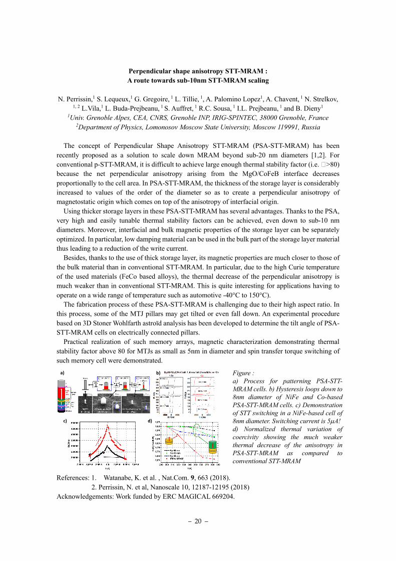
Perpendicular shape anisotropy STT-MRAM : A route towards sub-10nm STT-MRAM scaling
N. Perrissin,1 S. Lequeux,1 G. Gregoire, 1 L. Tillie, 1, A. Palomino Lopez1, A. Chavent, 1 N. Strelkov,
1, 2 L.Vila,1 L. Buda-Prejbeanu, 1 S. Auffret, 1 R.C. Sousa, 1 I.L. Prejbeanu, 1 and B. Dieny1 1Univ. Grenoble Alpes, CEA, CNRS, Grenoble INP, IRIG-SPINTEC, 38000 Grenoble, France
2Department of Physics, Lomonosov Moscow State University, Moscow 119991, Russia
The concept of Perpendicular Shape Anisotropy STT-MRAM (PSA-STT-MRAM) has been recently proposed as a solution to scale down MRAM beyond sub-20 nm diameters [1,2]. For conventional p-STT-MRAM, it is difficult to achieve large enough thermal stability factor (i.e. �>80) because the net perpendicular anisotropy arising from the MgO/CoFeB interface decreases proportionally to the cell area. In PSA-STT-MRAM, the thickness of the storage layer is considerably increased to values of the order of the diameter so as to create a perpendicular anisotropy of magnetostatic origin which comes on top of the anisotropy of interfacial origin.
Using thicker storage layers in these PSA-STT-MRAM has several advantages. Thanks to the PSA, very high and easily tunable thermal stability factors can be achieved, even down to sub-10 nm diameters. Moreover, interfacial and bulk magnetic properties of the storage layer can be separately optimized. In particular, low damping material can be used in the bulk part of the storage layer material thus leading to a reduction of the write current.
Besides, thanks to the use of thick storage layer, its magnetic properties are much closer to those of the bulk material than in conventional STT-MRAM. In particular, due to the high Curie temperature of the used materials (FeCo based alloys), the thermal decrease of the perpendicular anisotropy is much weaker than in conventional STT-MRAM. This is quite interesting for applications having to operate on a wide range of temperature such as automotive -40°C to 150°C).
The fabrication process of these PSA-STT-MRAM is challenging due to their high aspect ratio. In this process, some of the MTJ pillars may get tilted or even fall down. An experimental procedure based on 3D Stoner Wohlfarth astroïd analysis has been developed to determine the tilt angle of PSA-STT-MRAM cells on electrically connected pillars.
Practical realization of such memory arrays, magnetic characterization demonstrating thermal stability factor above 80 for MTJs as small as 5nm in diameter and spin transfer torque switching of such memory cell were demonstrated.
References: 1. Watanabe, K. et al. , Nat.Com. 9, 663 (2018). 2. Perrissin, N. et al, Nanoscale 10, 12187-12195 (2018) Acknowledgements: Work funded by ERC MAGICAL 669204.
a) b)
c) d)
Figure : a) Process for patterning PSA-STT-MRAM cells. b) Hysteresis loops down to 8nm diameter of NiFe and Co-based PSA-STT-MRAM cells. c) Demonstration of STT switching in a NiFe-based cell of 8nm diameter. Switching current is 5µA! d) Normalized thermal variation of coercivity showing the much weaker thermal decrease of the anisotropy in PSA-STT-MRAM as compared to conventional STT-MRAM

– 21 –
Spin-transfer switching and magnetic interactions in perpendicular magnetic tunnel junctions nanopillars
Andrew D. Kent
Center for Quantum Phenomena, Department of Physics, New York University, New York, NY 10003 [email protected]
Perpendicularly magnetized magnetic tunnel junctions (pMTJs) are very promising candidates for
high-density and non-volatile random access data storage. In order to achieve reliable and fast devices, as well as long-term thermal stability, the magnetization reversal mechanisms [1-2] and magnetic parameters of the pMTJ's free layer need to be characterized. We study the reversal mechanisms experimentally, by performing single-shot time-resolved measurements of circular pMTJs of varying sizes, allowing for precise extraction of the time when switching occurs (switching time, tsw ,50% conductance change), as well as the time needed to complete the switching process from 25% to 75% of the conductance change between the P and AP states (transition time, ttrans, see Fig. 1). In Fig. 1 we show exemplary data from a 70 nm diameter device transitioning from the P to the AP state, where the current flowing through the junction has been recorded in time, which characterizes the free layer magnetization projected onto the reference layer during the switching process. We observe ramp-like time traces (Fig. 1(a)), indicating the dominant switching mechanism to be domain wall propagation. The distributions of switching and transition times are shown in Fig. 1(b) and (c), respectively. A decrease in tsw and ttrans is observed with increasing pulse amplitude, as is reflected in the slope and onset time of the switches shown in (a). This means less time needed for the onset of switching and for completing it with increasing pulse amplitude. Assuming propagation of a domain wall across the sample width, the measured ttrans allow us to extract domain wall velocities of tens of m/s and to study their increase with increasing spin torque. We also characterize the spin-wave spectra in pMTJ free layers using spin-transfer FMR, which enables a measure of the exchange stiffness and estimates of the critical diameter for coherent spin-transfer switching [1].
Fig.1 (a) Three time traces at -0.5V, -0.7V and -0.85V pulse amplitudes showing increasingly fast reversal for increasing pulse amplitude. Switching (b) and transition (c) times extracted from 1000 time traces per voltage pulse level. Line color indicates the amplitude of the voltage pulse shown in (a). Acknowledgements Research was supported by Spin Memory and conducted in collaboration with Christian Hahn, Jamileh Beik Mohammadi and Jinting Hang at NYU and Georg Wolf, Bartek Kardasz, Steve Watts and Mustafa Pinarbasi at Spin Memory. References [1] G. D. Chaves-O’Flynn et al., Phys. Rev. Applied 4, 024010 (2015) [2] C. Hahn et al., Phys. Rev. B 94, 214432 (2016) [3] G. Wolf et al., Proc. SPIE 9167, Spintronics VII, 91671H (2014)
Fig. 1: (a) Three time traces at -0.5V, -0.7V and -0.85V showing increasingly faster reversal processes for increasingpulse amplitude. Switching (b) and transition (c) times extracted from 1000 time traces per voltage level. Line colorindicates the amplitude of the voltage pulse shown in (a).

– 22 –
Material and integration challenges of magnetic tunnel junctions in advanced spintronic applications
J. Swerts, S. Couet, R. Carpenter, E. Liu*, K. Hon, S. Mertens, K. Sankaran, S. Rao, W. Kim, K. Garello, S. Kundu, L. Souriau, F. Yasin, S. H. Sharifi, S. Van Elshocht, D. Crotti, and G. S. Kar
imec, Belgium. *currently at NUS, Singapore
The CoFeB/MgO/CoFeB based magnetic tunnel junction (MTJ) is the key component in many
spintronic devices that aim to replace conventional memory or logic devices. One of the MTJ-based devices, namely STT-MRAM, is currently being industrialized by major semiconductor foundries to replace embedded FLASH memory [1]. That breakthrough has been enabled by optimizing the MTJ stack to overcome major challenges encountered in CMOS processing such as back-end-of-line compatibility. The era of spintronics in semiconductor industry has begun. On the one hand the existing STT-MRAM MTJ stacks are being improved to extend its usage for next technologies nodes. On the other hand, other than E-Flash technologies, such as SRAM [2] are envisaged requiring specific properties of the STT-MRAM stack to be improved. In addition to STT-MRAM, alternative MTJ-based spintronic devices are being assessed for its strengths and weakness’ to replace or complement conventional technologies. Among them the spin-orbit-torque (SOT) MRAM where the MTJ is used for read-out, while writing occurs via current induced spin-orbit coupling in a 3-terminal device configuration. SOT-MRAM targets to replace L1/2 SRAM cache. Next to the device performance gaps that need to be addressed by materials and stack engineering, key integration challenges have to be solved to enable SOT-MRAM in a 300mm Si wafer production environment [3]. MTJ-based devices are also researched for logic applications. The domain-wall based spin-torque majority gate (DW-STMG) is one example [4]. Both SOT-MRAM and DW-STMG rely on a top-pinned MTJ stack design. That stack design differs from the stack currently being used in the STT-MRAM for E-Flash, which is the bottom pinned design. Recently, major progress in the thermal robustness of these top-pinned stacks [5, 6] has been reported paving the way for manufacturability of top-pinned based MTJ technologies.
In this paper, we review key development challenges for MTJ stacks in advanced spintronic applications with focus on the stack design, the materials, and their integration in 300mm Si wafer platforms.
References: [1] M. Lapedus, “Four foundries back MRAM”, Semiconductor Engineering (Aug 23rd,2017). [2] S. Sakhare et al. IEDM 18-3 (2018), [3] K. Garello et al., VLSI (2018) [4] M. Manfrini et al. AIP Advances 8 (5), 055921 9 (2018). [5]. J. Swerts et al. IEDM, 38-6 (2017). [6] E. Liu et al., Phys. Rev. Applied 10, 054054 (2018).

– 23 –
Spin current generation, detection, and transport with antiferromagnets
Axel Hoffmannc Materials Science Division, Argonne National Laboratory, Argonne, IL 60439, USA
Harnessing spin currents is a promising pathway towards low-power electronics [1]. Towards this
end, it recently has been recognized that antiferromagnetic materials can play a more active role beyond their traditional use for providing a reference magnetization direction via exchange bias. Namely, antiferromagnets may be conduits for spin currents, as well as, actively enable spin current generation and detection [2]. With respect to the later, we demonstrated spin current generation both via spin Hall effects in conducting antiferromagnets and spin Seebeck effects in insulating antiferromagnets. Using CuAu-I-type metallic antiferromagnets (PtMn, IrMn, PdMn, and FeMn) we showed by using spin pumping that these alloys have significant spin Hall effects, which in the case of PtMn become comparable to the ubiquitously used Pt [3]. The spin Hall angles increase for the alloys with heavier element; a behavior that is well reproduced by first-principle calculations of the spin Hall conductivities based on intrinsic spin Hall effects. Furthermore, the calculations suggest pronounced anisotropies of the spin Hall conductivities, which we tested using spin transfer torque ferromagnetic resonance measurements using epitaxially grown antiferromagnetic films [4]. We observe that indeed the spin Hall conductivity is maximized for different growth orientations (a-axis for PtMn and PdMn, and c-axis for IrMn) in accordance with the first principle calculations. Interestingly, despite this striking anisotropy the influence of the exact microscopic antiferromagnetic spin structures appears to have a negligible influence on the spin orbit torques [5]. In addition, using spin pumping measurements with permalloy/FeMn/W trilayers, we observe that there are two distinct mechanism for transporting a spin current in the metallic antiferromagnet, which we associate with electronic and magnonic spin transport, respectively [6].
This work was supported by the U.S. DOE, Office of Science, Materials Sciences and Engineering Division, French Projet d’Investissement d’Avenir project “Lorraine Université d’Excellence,” Project No. ANR-15-IDEX-04-LUE, and DFG. [1] A. Hoffmann and S. D. Bader, Phys. Rev. Appl. 4, 047001 (2015). [2] J. Železný, P. Wadley, K. Olejník, A. Hoffmann, and H. Ohno, Nature Phys. 14, 220 (2018). [3] W. Zhang, M. B. Jungfleisch, W. Jiang, J. E. Pearson, A. Hoffmann, F. Freimuth, and
Y. Mokrousov, Phys. Rev. Lett. 113, 196602 (2014). [4] W. Zhang, M. B. Jungfleisch, F. Freimuth, W. Jiang, J. Sklenar, J. E. Pearson, J. B. Ketterson,
Y. Mokrousov, and A. Hoffmann, Phys. Rev. B 92, 144405 (2015). [5] H. Saglam, J. C. Rojas-Sanchez, S. Petit, M. Hehn, W. Zhang, J. E. Pearson, S. Mangin, and
A. Hoffmann, Phys. Rev. B 98, 094407 (2018). [6] H. Saglam, W. Zhang, M. B. Jungfleisch, J. Sklenar, W. Jiang, J. E. Pearson, J. B. Ketterson, and
A. Hoffmann, Phys. Rev. B 94, 140412(R) (2016).
Session 5: Magnetic Skyrmions Chair: Gonzalo Vallejo-Fernandez 09:00~10:00 (P/X 001)

– 24 –
Lorentz microscopy study of hybrid walls and skyrmion nucleation in multilayer materials
Kayla Fallon, Sean Hughes, Damien McGrouther, Samuel McFadzean, William Smith, and Stephen McVitie
SUPA School of Physics and Astronomy, University of Glasgow, Glasgow, G12 8QQ, United Kingdom
Katharina Zeissler and Christopher Marrows School of Physics and Astronomy, University of Leeds, Leeds, LS2 9JT, United Kingdom
William Legrand, Fernando Ajejas, Davide Maccariello, Sophie Collin, Nicolas Reyren, and Vincent Cros Unité Mixte de Physique, CNRS, Thales, Univ. Paris-Sud, Université Paris-Saclay, 91767,
Palaiseau, France
Skyrmions are the subject of intense current interest with those supported in magnetic multilayer systems likely to provide potential for future applications as memory and logic devices. We report on transmission electron microscope (TEM) studies of detailed of the wall structure and skyrmion nucleation at nanoscale defect sites in polycrystalline magnetic multilayer samples with interfacial exchange. The latter are created in a controlled manner with focused ion beam (FIB) irradiation. Using the FIB method we are able to nucleate compact individual skyrmions local to the point artificial defect sites and, for specific ion doses, these remain stable both at room temperature and in zero applied magnetic field. The size of the skyrmion nucleated by this method matches that supported by the unmodified material system where the skynrmions appear at random positions during reversal - in this case between 100 and 200 nm. The physical, compositional and magnetic structure of the defects and skyrmions are characterised using a range of transmission electron microscopy techniques. This provides a correlation of the effect on dose on the nature of the defect and its influence on the behaviour of the skyrmions. Results ate presented from two different film systems with doses varying over 3 orders of magnitudewhich will show the best conditions for the controlled skyrmion nucleation.
Additionally we report on the detailed domain wall structure in such multilayer films. Depending on the multilayer stack geometry we are able to identify walls as either pure Néel or hybrid types. The latter are a mixture of internal Bloch and surface Néel contributions in a structure that provides a flux closure structure through the stack thickness. We report on the variation of wall structure with stack geometry using quantitative Lorentz TEM microscopy in conjunction with other microscopic methods.

– 25 –
Spin-caloritronics in ordered-alloy thin films
Koki Takanashi1,2, Masaki Mizuguchi1,2,3, Takeshi Seki1,2 1Institute for Materials Research, Tohoku University
2Center for Spintronics Research Network, Tohoku University 3CREST, Japan Science and Technology Agency
Spin-caloritronics, which concerns the interplay between spin, charge and heat, has attracted much
attention as a development of spintronics. Anomalous Nernst effect (ANE), which induces an electric voltage in the direction perpendicular to both temperature gradient and magnetization, is one of well-known classical thermomagnetic phenomena. However, there have been only a few studies on ANE for metals and alloys. From the viewpoint of modern spin-caloritronics, we may say ANE is a phenomenon that a spin current induced by temperature gradient is converted into an electric current in the transverse direction due to inverse spin Hall effect.
In this work, systematic investigation of ANE has been made for perpendicularly magnetized ordered-alloy thin films, compared with uniaxial magnetic anisotropy (Ku) and anomalous Hall effect (AHE). 30 nm-thick L10-FePt, L10-FePd L10-MnGa and D022-Mn2Ga thin films were prepared on MgO(001) substrates by sputtering. The ANE increases with temperature although the signs of ANE for Fe-based ordered alloys are opposite to those for Mn-based ordered alloys. Ordered alloys with higher Ku show higher ANE, suggesting high Ku materials are suitable for thermoelectric applications [1]. The temperature dependence of ANE and AHE for L10-FePt follows the Mott relation at low temperatures (<100 K); however ANE is remarkably enhanced in comparison with the Mott relation at high temperatures. This enhancement of ANE is explained from a model: magnon spin current induced by temperature gradient is converted into conduction-electron spin current via s-d interaction, giving additional contribution to ANE [2]. Recently we have also succeeded in the observation of anomalous Ettingshausen effect as a reciprocal phenomenon of ANE through the use of lock-in thermography [3,4]. [1] K. Hasegawa et al., Appl. Phys. Lett., 106 (2015) 242405. [2] M. Mizuguchi et al., arXiv:1804.03751. [3] T. Seki et al., Appl. Phys. Lett., 112 (2018) 152403. [4] T. Seki et al., J. Phys. D: Appl. Phys., 51 (2018) 254001.
Session 6: Material Development for Spintronic Devices Chair: Takahide Kubota 11:10~12:50 (P/X 001)

– 26 –
Spintronic Devices: From Material Development to Characterisation
Atsufumi Hirohata Department of Electronic Engineering, University of York
Since the development of magnetic random access memory using spin-transfer torque reached its
commercialisation phase, spintronics has entered a new era. For further improvement of spintronic devices, a new ferromagnetic material with a small damping constant below 0.001 and 100% spin polarisation is required to be developed in a film form at room temperature [1]. Especially, Heusler alloys have been attracting intensive attention to satisfy these requirements by crystallising it into a perfectly ordered phase [2].
We have recently developed a new process to reduce the crystallisation temperature down to 80ºC for a Heusler alloy films grown on the (110) seed layer [3], which is compatible with the current memory fabrication process. Giant magnetoresistive junctions consisting of Co2FeAl0.5Si0.5/Ag/Co2FeAl0.5Si0.5 show only a small resistance change but their structures can be optimised. In such a junction, the corresponding switching current density was demonstrated to be reduced by replacing oxide insulating layers to isolate top and bottom electrodes by a ferromagnetic oxide layer to induce spin wave to assist the current-induced magnetisation switching.
These junctions were characterised by non-destructive imaging with scanning electron microscopy we developed [4]. We managed to improve the yield of such junctions by 15% by identifying the cause of damages with our imaging technique. These results pave a way for further improvement of the spintronic devices.
This work was supported by Seagate Technology, EPSRC-JSPS Core-to-Core Programme (EP/M02458X/1) and JST CREST Programme (No. JPMJCR17J5). References [1] A. Hirohata and K. Takanashi, J. Phys. D: Appl. Phys. 47, 193001 (2014). [2] C. Felser and A. Hirohata (Eds.), Heusler Alloys (Springer, Berlin, Germany, 2016). [3] W. Frost et al., J. Magn. Magn. Mater. 484, 100 (2019). [4] E. Jackson et al., Sci. Rep. 8, 7585 (2018).

– 27 –
Significant TMR oscillation effect in magnetic tunnel junctions with a MgAl2O4 barrier
H. Sukegawa and S. Mitani National Institute for Materials Science, 1-2-1 Sengen, Tsukuba 305-0047, Japan
MgO-based magnetic tunnel junctions (MTJs) exhibiting a giant tunnel magnetoresistance (TMR) effect have been widely implemented in various spintronic applications. Nevertheless, there remains “a long-standing puzzle” in MgO-based MTJs; TMR ratio significantly oscillates with respect to a barrier thickness. Surprisingly, the oscillation period is always close to 0.3 nm, independent of an atomic monolayer thickness of MgO(001). This peculiar behavior is observed not only in Fe/MgO/Fe(001) [1] but also in Co-based Heusler alloy MTJs [2]. So far, many theoretical approaches have failed to reproduce this effect completely. These situations make it difficult to specify the physical origin of the oscillation. Investigations using barrier materials other than MgO would be necessary for understanding the possible origin further.
In this talk, we will introduce our recent experimental trials using a new epitaxial barrier, MgAl2O4 (spinel) to achieve better lattice-matching between Fe electrodes and a barrier [3]. An Fe/MgAl2O4/Fe(001) MTJ structure can have lattice-matched and atomically-flat interfaces, enabling us to highlight the oscillation effect. We fabricated micrometer-size MTJs with a stack structure of MgO(001) substrate/Cr (40 nm)/Fe (100 nm)/MgAl2O4 (tMAO)/Fe (7 nm)/IrMn (12 nm)/Ru cap using a magnetron sputtering system. A wedge-shaped MgAl2O4 barrier was prepared by a linear motion shutter equipped with the sputtering system to evaluate tMAO dependences of a TMR ratio [3]. A typical TMR ratio was 220% at 300 K (390% at 5 K).
We observed strong oscillatory behavior of a TMR ratio with the period tMAO ~ 0.3 nm at 300 K and 5 K, almost identical to the MgO-based MTJs. The oscillation amplitude in the TMR ratio reaches 30% at 300 K (60% at 5 K), much larger than an Fe/MgO/Fe (10% at 293 K) [1]. In addition to the TMR oscillation, we found that tunnel anisotropic magnetoresistance (TAMR), the conductance difference between in-plane and perpendicular magnetized states, also oscillated with almost the same period (tMAO ~ 0.3 nm). These results suggest close correlation between TMR and TAMR origins. This work was partly supported by the ImPACT Program of Council for Science, Technology and Innovation, Japan, and JSPS KAKENHI Grant 16H06332. References: [1] S. Yuasa et al., Nat. Mater. 3, 868 (2004). [2] T. Marukame et al., Phys. Rev. B 81, 134432 (2010). [3] M. Belmoubarik et al., Appl. Phys. Lett. 108, 132404 (2016).

– 28 –
Effect of Surface Anisotropy on Magnetic Domain Formation at the Surface of Fe3O4(001)
Phillip Bentley1, Jason Zhang1, Xia Sun2, Mitsunori Kurahashi3, Andrew Pratt1,3, and Yasushi Yamauchi3
1. Department of Physics, University of York, York YO10 5DD, U.K. 2. University of Science and Technology of China, Hefei, Anhui 230026, China 3. National Institute for Materials Science, Tsukuba, Ibaraki 305-0047, Japan
Imaging the domain structure at the native surface of magnetic materials is important for
understanding their potential application to spintronic device fabrication. Due to the relaxation and reconstruction of surface atoms, surface magnetic properties such as the Fermi-level spin polarization, P(EF), can be drastically different to the bulk and so techniques that are sensitive to outermost atoms only are desirable. Previously, we introduced the new technique of spin-polarized metastable emission electron microscopy (SPMEEM) which achieves this task by using a beam of spin-polarized helium atoms prepared in the metastable 23S state (19.82 eV). When approaching to just a few Å above a surface, these atoms de-excite through one of two different Auger electron processes yielding extreme surface sensitivity. This novel approach to domain imaging complements the capabilities of spin-polarised low-energy electron microscopy (SPLEEM) and spin polarized photoemission electron microscopy (SPPEEM) in analyzing magnetic materials.
Here, we discuss the application of SPMEEM to the study of the domain structure at the surface of Fe3O4(100), a material in which bulk half-metallicity (P(EF)=-100%) is significantly reduced at the surface due to a deep surface reconstruction and the presence of unsaturated oxygen dangling bonds. In addition to mapping the spin polarization, we show that the magnetization vector at the surface has a significant out-of-plane component suggesting that the surface easy axis is canted more than previously believed [2]. We discuss how magnetocrystalline anisotropy in the bulk favours a <111> easy axis direction and how dipolar forces at the surface lead to some degree of in-plane magnetisation with a preferred <110> easy axis. Such results demonstrate the potential of SPMEEM in determining the detailed balance between these contributions to surface anisotropy and the magnetic properties of a material. [1] A. Pratt, M. Kurahashi, D. Gilks, X. Sun, and Y. Yamauchi, Phys. Rev. B 85, 180409(R) (2012) [2] L. Martin-Garcia, G. Chen, Y. Montana, A. Mascaraque, B. M. Pabón, A. K. Schmid, and J. de la Figuera, Sci. Rep. 8, 5991 (2018)

– 29 –
Magnon and phonon-polariton excitations in multiferroic BiFeO3
Takuya Satoh1,2*, Pritam Khan2,3, Masataka Kanamaru2, Keita Matsumoto2, Toshimitsu Ito4 1 Department of Physics, Tokyo Institute of Technology, Tokyo 152-8551, Japan
2 Department of Physics, Kyushu University, Fukuoka 819-0395, Japan 3 Department of Physics, University of Limerick, V94 T9PX Limerick, Ireland
4 National Institute of Advanced Science and Technology (AIST), Ibaraki 305-8562, Japan E-mail: [email protected]
In condensed matter physics, magnetism and ferroelectricity are the two most popular representative subjects. Bismuth ferrite (BiFeO3) is a widely studied compound which exhibits simultaneous ferroelectric and antiferromagnetic order with potential applications in spintronic devices. Owing to its ferroelectricity and consequent piezoelectric coupling BiFeO3 offers strong driving force for initiating coherent phonons. Several magnon modes were also reported using spontaneous Raman scattering. In this study, we show that coherent magnons and phonon can be photoexcited and photodetected by using the combination of linearly polarized femtosecond pump and circularly polarized probe, respectively (Fig. 1). The Fourier transform amplitude spectrum of time-resolved polarization curve reveals that the center frequencies of the oscillations are 0.53, 0.56, 0.74, and 2.4 THz. A phenomenological symmetry-based theory reveals that 2.4-THz oscillations belongs to E phonon modes. Successive temperature dependence of 2.4-THz mode does not exhibit any noticeable change in frequency, therefore confirms its phonon nature. However, on the other hand, the lifetime of the coherent phonon decreases steadily from 17.3 to 3.8 ps, when the temperature is raised from 80 to 300 K. The 0.53-, 0.56-, and 0.74-THz modes were attributed to Ψ1
(2), Ψ1(1), and Φ2 magnons from
the temperature dependence of the center frequencies. We also employed time-resolved imaging technique on BiFeO3 and found that phonon-polariton like excitation propagated out of the pump spot with the phase velocity of 20% of light velocity in BiFeO3.
Magnon and phonon-polariton excitations in multiferroic BiFeO3
Takuya Satoh1,2*, Pritam Khan2,3, Masataka Kanamaru2, Keita Matsumoto2, Toshimitsu Ito4
1 Department of Physics, Tokyo Institute of Technology, Tokyo 152-8551, Japan 2 Department of Physics, Kyushu University, Fukuoka 819-0395, Japan
3 Department of Physics, University of Limerick, V94 T9PX Limerick, Ireland 4 National Institute of Advanced Science and Technology (AIST), Ibaraki 305-8562, Japan
E-mail: [email protected]
In condensed matter physics, magnetism and ferroelectricity are the two most popular
representative subjects. Bismuth ferrite (BiFeO3) is a widely studied compound which exhibits simultaneous ferroelectric and antiferromagnetic order with potential applications in spintronic devices. Owing to its ferroelectricity and consequent piezoelectric coupling BiFeO3 offers strong driving force for initiating coherent phonons. Several magnon modes were also reported using spontaneous Raman scattering. In this study, we show that coherent magnons and phonon can be photoexcited and photodetected by using the combination of linearly polarized femtosecond pump and circularly polarized probe, respectively (Fig. 1). The Fourier transform amplitude spectrum of time-resolved polarization curve reveals that the center frequencies of the oscillations are 0.53, 0.56, 0.74, and 2.4 THz. A phenomenological symmetry-based theory reveals that 2.4-THz oscillations belongs to E phonon modes. Successive temperature dependence of 2.4-THz mode does not exhibit any noticeable change in frequency, therefore confirms its phonon nature. However, on the other hand, the lifetime of the coherent phonon decreases steadily from 17.3 to 3.8 ps, when the temperature is raised from 80 to 300 K. The 0.53-, 0.56-, and 0.74-THz modes were attributed to Ψ1
(2), Ψ1(1), and
Φ2 magnons from the temperature dependence of the center frequencies. We also employed time-resolved imaging technique on BiFeO3 and found that phonon-polariton like excitation propagated out of the pump spot with the phase velocity of 20% of light velocity in BiFeO3.
Fig.1 Time-resolved ellipticity change (Δη) of transmitted probe polarization at probe delays of (a) 20 and (b) 60 ps. The insets show the FFT amplitude spectra of the signal.
Session 7: Antiferromagnetic Spintronics Chair: Masafumi Shirai 14:20~15:40 (P/X 001)

– 30 –
Topological Antiferromagnetic Spintronics: Crystal Hall Antiferromagnets
Libor Šmejkal INSPIRE group, Johaness Gutenberg Universitat, Mainz, Germany
Departments of Spintronics and Nanoelectronics, Institute of Physics, Czech Academy of Sciences, Prague, Czech Rep.
The family of Hall effects, even 140 years after its first member was discovered, continue to play a
central role in condensed matter research for its fascinating topological, relativistic, and quantum mechanical nature as well as prospective nanoelectronic applications [1,2]. The spontaneous Hall effect was in last decade observed also in certain noncoplanar spin liquid candidates and noncollinear antiferromagnets cementing the notion of spontaneous topological and spontaneous anomalous Hall antiferromagnets [1, 2 and Refs therein].
In this talk, we will introduce a complementary mechanism in crystals whose magnetic structure alone generates no Hall response and the required breaking of time-reversal and other symmetries is caused by the combined effect of trivial magnetic order and the arrangement of non-magnetic atoms in the lattice [3]. We identify notorious collinear antiferromagnets hosting this crystal Hall effect [3] in its pristine form, which were previously anticipated to be prevented from any spontaneous Hall signals. We will classify the crystal Hall antiferromagnets, list materials candidates and discuss experimental signatures of the effect.
In the last part of the talk, we will outline future directions of the emerging field of topological antiferromagnetic spintronics [1,2], including research of Dirac-Neel antiferromagnets [4,5]. Dirac – Neel antiferromagnets, e.g. CuMnAs and Mn2Au, can simultaneously host Dirac quasiparticle electronic structure and Neel spin-orbit torques allowing for the THz control of antiferromagnetic order and relativistic metal-insulator transition. [1] LŠ and T. Jungwirth, Symmetry and topology in antiferromagnetic spintronics, Topology in Magnetism, Eds. J. Zang, V. Cros, A. Hoffmann, Springer International Publishing (2018) [2] LŠ, Yuriy Mokrousov, Binghai Yan, Allan H. MacDonald, Topological antiferromagnetic spintronics, Nature Physics 14, 242–251 (2018) [3] LŠ, Rafael Gonzalez-Hernandez, Tomas Jungwirth, Jairo Sinova, arXiv:1901.00445 (2019) [4] S. Yu. Bodnar, LŠ, I. Turek, T. Jungwirth, O. Gomonay, J. Sinova, A.A. Sapozhnik, H.-J. Elmers, M. Kläui, M. Jourdan, Writing and Reading antiferromagnetic Mn2Au: Néel spin-orbit torques and large anisotropic magnetoresistance, Nature Communications 9, 348(2018) [5] LŠ, J. Železný, J. Sinova, T. Jungwirth, Electric control of Dirac quasiparticles by spin-orbit torque in an Antiferromagnet, Phys. Rev. Lett. 118 (2017) 106402-106402.
– 31 –
A Theoretical Proposal of an In-memory Spin-Wave Logic Gate for All Boolean Operations
Weichao Yu Tohoku University
In the conventional von-Neumann computing architecture, the data storage and data processing are
separately realized in the memory and the central processing unit, communicating via the data bus. This separated architecture limits the computing speed and the energy efficiency. Here we introduce a computing concept of purely magnetic nature, which seamlessly integrates the memory and processing by employing the static magnetic texture for the data storage, and its collective excitation the spin wave for processing. Based on this processing-in-memory spin wave computing architecture, we propose an instruction-based universal logic gate, which realizes all unary and binary operations in one single structure. The spin-wave logic gate proposed here also sets a model for the future energy efficient non-volatile computing, the distributed processing-in-memory computing, and the evolvable neuromorphic computing.
– 32 –
Topological Transition in Rashba Spin Interferometers
Fumiya Nagasawa1, Henri Saarikoski2, Diego Frustaglia3, Junsaku Nitta1,4
1Department of Materials Science, Tohoku University, Japan 2 RIKEN Center for Emergent Matter Science, Japan
3Departamento de Física Aplicada II, Universidad de Sevilla, E-41012, Sevilla, Spain 4Center for Spintronics Research Network, Tohoku University, Japan
Spin-orbit interaction (SOI) plays crucial roles in diverse fields of condensed matter, including the
investigation of Majorana fermion, topological insulator, quantum information, and spintronics [1]. In III-V compound semiconductor heterostructures, there are two contributions to SOI, namely Rashba and Dresselhaus SOI due to structural and bulk inversion asymmetry, respectively. They each induce an effective magnetic field, the directions of which depend on the electron's momentum. Especially, the Rashba SOI is quite important since the strength is controlled by gate electric fields.
The Aharonov–Casher (AC) spin interference has been demonstrated in Rashba ring array [2]. By applying an in-plane magnetic field, a phase shift of the AC interference pattern towards the small SOI regions is observed. A perturbation theory for a one-dimensional Rashba ring under small in-plane fields reveals that the phase shift originates exclusively from the modulation of a pure geometric phase component of the electron spin independently from dynamical phases. The phase shift is well reproduced by perturbation theory and non -perturbative transport simulations [3]. Here, we investigate the AC spin interference by varying the Rashba SOI strength and in-plane field direction. Anisotropic spin interference depending on the in-plane field direction is observed, manifesting the coexistence of Rashba and Dresselhaus SOIs. The anisotropy shows either maximum or minimum at the in-plane field angle with respect to [100] direction. The anisotropy is reversed by varying the Rashba SOI strength while the sign of the Rashba SOI is unchanged. Anisotropy measurements in an AC spin interferometer can be utilized to reveal signatures of spin dynamic and geometric phases [4].
Topological transition in the Rashba spin interferometer under an in-plane Zeeman field has been proposed [5] on the basis of the spin geometric phase switching. The transitions are determined by the topology of the fields texture through an effective Berry phase (related to the winding parity of spin modes around poles in the Bloch sphere), irrespective of the actual complexity of the nonadiabatic spin dynamics. We discuss ways to realize topological transition in InGaAs-based quantum rings and squares with Rashba SOI and in-plane Zeeman field. [1] A. Manchon, H. C. Koo, J. Nitta, S. M. Frolov, and R. Duine, Nat. Mater. 14, 871 (2015). [2] F. Nagasawa, J. Takagi, Y. Kunihashi, M. Kohda, and J. Nitta, Phys. Rev. Lett. 108, 086801 (2012). [3] F. Nagasawa, D. Frustaglia, H. Saarikoski, K. Richter, and J. Nitta, Nat. Commun. 4, 3526 (2013). [4] F. Nagasawa, H. Saarikoski, D. Frustaglia, and J. Nitta, Phys. Rev. B 98, 245301 (2018). [5] H. Saarikoski, F. Nagasawa, J. Nitta, and D. Frustaglia, Phys. Rev. B 91, 241406(R) (2015).
Session 8: 2D Spin Devices and Topological Effects Chair: Shigemi Mizukami 16:00~17:50 (P/X 001)

– 33 –
Gate-tunable charge-to-spin interconversion in atomically-thin van der Waals heterostructures at room temperature
Aires Ferreira1
1 Department of Physics, University of York, York YO10 5DD, United Kingdom, [email protected]
The strong interplay between pseudospin and spin degrees of freedom in atomically thin materials
holds unique prospects for spintronics [1,2,3]. In graphene/semiconducting group-VI dichalcogenide bilayers, a proximity-induced spin-orbit coupling on graphene in the range 0.1 - 1 meV has been probed in recent transport measurements [4,5]. However, the emergence of a spin-momentum-locked electronic structure, pivotal for efficient electrical control of the electron’s spin [2], has remained elusive.
In this talk, I will present a van der Waals heterointerface formed between graphene and metallic layered compound 2H-TaS2 that hosts 2D Dirac states with a giant spin-orbit splitting. The graphene/2H-TaS2 bilayer is shown to support current-driven spin polarization, a relativistic transport phenomenon known as inverse spin galvanic effect (ISGE). Detailed quantum transport calculations show that the charge-to-spin conversion efficiency can be as great as 30% at room temperature. Owing to minimal charge transfer across the graphene/2H-TaS2 heterointerface, the non-equilibrium spin polarization can be fully reversed by a back-gate voltage. The ISGE gate-tunability is an elegant manifestation of entanglement between spin and lattice-pseudospin degrees of freedom arising from broken mirror inversion symmetry in two-dimensional materials. Implications for on-going experimental efforts in the field, including a new spin precession protocol for unambiguous detection of spin Hall effect and ISGE contributions to nonlocal resistances [6], will be briefly discussed. [1] Soumyanarayanan, A., Reyren, N., Fert A. & Panagopoulos, C. Emergent phenomena induced by spin-orbit coupling at surfaces and interfaces. Nature 539, 509 (2016). [2] Offidani, M., Milletari, M., Raimondi, R. & Ferreira, A. Optimal charge-to-spin conversion in graphene on transition-metal dichalcogenides. Physical Review Letters 119, 196801 (2017). [3] Offidani, M. & Ferreira, A. Anomalous Hall effect in 2D Dirac Materials. Physical Review Letters 121, 126802 (2018). [4] Avsar, A. et al. Spin-orbit proximity effect in graphene. Nature Communications 5, 4875 (2014). [5] Wang, Z. et al. Origin and magnitude of ‘designer’ spin-orbit interaction in graphene on semiconducting transition metal dichalcogenides. Physical Review X 6, 041020 (2016). [6] M. Offidani et al. Submitted (2019).

– 34 –
Size Dependence of the Influence of Edge Effects in Nanoscale Perpendicular-Anisotropy Magnetic Tunnel Junctions
J. Igarashi1, M. Shinozaki1, J. Llandro1-3, S. Fukami1-6, H. Sato1-4, and H. Ohno1-5
1Laboratory for Nanoelectronics and Spintronics, Research Institute of Electrical Communication, Tohoku University, 2-1-1 Katahira, Aoba-ku, Sendai 980-8577 Japan. 2Center for Science and Innovation in Spintronics, Tohoku University, 2-1-1 Katahira, Aoba-ku, Sendai 980-8577 Japan. 3Center for Spintronics Research Network, Tohoku University, 2-1-1 Katahira, Aoba-ku, Sendai
980-8577 Japan.4Center for Innovative Integrated Electronic Systems, Tohoku University, 468-1 Aramaki Aza Aoba, Aoba-ku, Sendai 980-0845 Japan.5WPI-Advanced Institute for Materials
Research, Tohoku University, 2-1-1 Katahira, Aoba-ku, Sendai 980-8577 Japan.
In CoFeB/MgO-based perpendicular MTJs, edge effects such as inhomogeneous stray fields and process-induced variations of edge properties must be considered in order to understand the magnetization switching behavior as the junction diameter is reduced. We report the results of investigations into the influences of these factors as a function of junction size on both field-induced and current-induced switching by employing two types of MTJ: step structures with a reference layer much larger than the free layer fabricated using a short ion milling time, and standard structures in which the reference and free layers are almost the same size made using a longer ion milling time. We study the differences between step and standard MTJs in the dependences of coercivity HC and switching current density JC versus out-of-plane magnetic bias field Hout on the diameter D of the circular free layer.
From all measurements, the step structures followed closely the expected coherent reversal model. However, measurements of the magnetic field–angle dependence of coercivity HC revealed that for D < 20 nm, standard structures do not follow the coherent rotation model. Micromagnetic simulations found that the differences could be best explained by a reduction of the effective magnetic anisotropy Keff around the free layer edge and that in comparison the influence of the reference layer stray field was small [1]. We also found that the dependence of JC on Hout showed increasingly different trends for the two structures as D was reduced below 45 nm. Measurements of the dependence of homodyne-detected ferromagnetic resonance on D revealed that the averaged Keff of the standard structure was smaller than that of the step structure and that again the difference became larger as D was reduced [2].
This work was supported in part by ImPACT Program of CSTI, JST-OPERA, JSPS KAKENHI 16K18084, and DIARE. J.L. and J.I. would like to acknowledge support from GP-Spin at Tohoku University. [1] J. Igarashi, J. Llandro, H. Sato, F. Matsukura and H. Ohno, APL 111, 132407 (2017). [2] M. Shinozaki, J. Igarashi, H. Sato and H. Ohno, APEX 11, 043001 (2018).

– 35 –
Skyrmions in chiral magnetic multilayers
Katharina Zeissler1, Simone Finizio2, Kowsar Shahbazi1, Jamie Massey1, Fatma Al Ma’Mari1, Alexandra Huxtable1, David Bracher2, Armin Kleibert2, Sebastian Wintz1,3, Sina Mayr1,4, Teresa
Weßels5, Alexandr Sadovnikov6, Mark Rosamond7, Edmund Linfield7, Thomas Moore1, Jörg Raabe2, Gavin Burnell1,and Christopher Marrows1*
1School of Physics and Astronomy, University of Leeds, Leeds LS2 9JT, United Kingdom2Swiss Light Source, Paul Scherrer Institute, 5232 Villigen, Switzerland3Institute of Ion Beam Physics
and Materials Research,Helmholtz-Zentrum Dresden-Rossendorf, 01328 Dresden, Germany4Department of Materials, Laboratory for Mesoscopic Systems, ETH Zürich, 8093
Zürich, Switzerland5Ernst Ruska-Centre for Microscopy and Spectroscopy with Electrons and Peter Grünberg Institute, Forschungszentrum Jülich, 52425 Jülich, Germany6Laboratory
“Metamaterials”, Saratov State University, Saratov, 410012, Russia7School of Electronic and Electrical Engineering, University of Leeds,Leeds LS2 9JT, United Kingdom
Magnetic skyrmions are topologically-nontrivial spin textures with particle-like properties1. Their
size, topological stability, and mobility suggest their use in future generations of spintronic devices, the prototype of which is the skyrmion racetrack2. To realise a racetrack requires three basic operations: the nucleation (writing), propagation (manipulation), and detection (reading) of a skyrmion, all by electrical means. Here we show that all three are experimental feasible at room temperature in Pt/Co/Ir or Pt/CoB/Ir multilayers in which the different heavy metals above and below the magnetic layer break inversion symmetry and induce chirality by means of the Dzyaloshinskii-Moriya interaction, defining the structure of Néel skyrmion spin textures3. We show deterministic nucleation on nanosecond timescales using an electrical point contact on top of the multilayer4 (Figure 1), current-driven propagation along a wire in which they are channelled by defects in the multilayer, and detection by means of the Hall effect (Figure 2) that reveals an unexpectedly large contribution to the Hall signal that correlates with the topological winding number5. 1Nagaosa, N. & Tokura, Y. (2013). Topological properties and dynamics of magnetic skyrmions. Nat. Nanotech. 8, 899. 2Fert, A. et al. (2013). Skyrmions on the track. Nature Nanotech. 8, 152. 3Zeissler, K. et al. (2017). Pinning and hysteresis in the field dependent diameter evolution of skyrmions in Pt/Co/Ir superlattice stacks. Sci. Rep. 7, 15125. 4Finizio, S. et al., Deterministic field-free skyrmion nucleation at a nano-engineered injector device. arXiv:1902.10435. 4Zeissler, K, et al. (2018). Discrete Hall resistivity contribution from Néel skyrmions in multilayer nanodiscs. Nature Nanotech. 13, 1161.
Figure 1. STXM images before and after nucleation of a skyrmion at a 500 nm wide point
contact to a Pt/CoB/Ir multilayer.
Figure 2. STXM image of two skyrmions in a electrically-connected 1 µm diameter Pt/Co/Ir
multilayer dot. 500 nm scale bar.
– 36 –
Magnetic tunnel junction with a manganese nano-layer
Shigemi Mizukami1,2,3
1 WPI Advanced Institute for Materials Research, Tohoku University, Japan 2Center for Spintronics Research Network, Tohoku University, Japan
3Center for Science and Innovation in Spintronics (CSIS), Core Research Cluster (CRC), Tohoku University, Japan
A magnetic tunnel junction with a perpendicular magnetic easy axis is a key device for spintronic
memory applications. In this talk, we show recent research results on magnetic tunnel junction with a magnetic nanolayer with a perpendicular magnetic easy axis and negligible magnetization [1]. Even though a manganese metal is paramagnetic or antiferromagnetic in bulk form, a few manganese monolayers grown on a paramagnetic ordered alloy template and capped by an oxide layer exhibit a strong perpendicular magnetic anisotropy field exceeding 19 T as well as a negligible magnetization of 25 kA/m. The nanolayer shows tunnel magnetoresistance at room temperature. Further the perpendicular magnetic anisotropy for the nanolayer can be reduced by applying an electric voltage for the junction. These findings will provide new insight into a creation of new nanolayer magnets. This work was partially supported by the ImPACT program and KAKENHI. [1] K. Z. Suzuki, S. Kimura, H. Kubota, and S. Mizukami, ACS Appl. Mater. Interfaces 10, 43305 (2018).
Session 9: Heusler-Alloy Devices Chair: Mikihiko Oogane 09:00~11:00 (P/X 001)

– 37 –
Enabling BEOL Compatibility in Top-Pinned STT-MRAM R. Carpenter, J. Swerts, S. Couet, K. Hon, S. Mertens, K. Sankaran, S. Rao, W. Kim, K. Garello, S.
Kundu, L. Souriau, F. Yasin, S. H. Sharifi, S. Van Elshocht, D. Crotti, and G. S. Kar Imec, Belgium
Perpendicular Magnetic Tunnel Junctions (MTJ) are widely researched as a key component in Spin
Transfer Torque Magnetic Random-Access Memory (STT-MRAM). Bottom Pinned (BP) MTJs (fig 1.a) are the favoured design due to their compatibility with Back End of Line (BEOL) processing temperatures up to 400°C [1-4]. Their annealing tolerance is due to the robust Synthetic AntiFerromagnetic (SAF) pinning layer (PL) that is grown on a (111) texture inducing seed to obtain a high perpendicular magnetic anisotropy (PMA). For a top pinned (TP) MTJ (fig 1.b/1.c) design the PL is grown on top of the (100) textured CoFeB/MgO/CoFeB MTJ giving poor seeding and therefore insufficient robustness at 400°C. Despite this disadvantage, TP MTJs are still studied as they are a vital component in alternative MRAM e.g. Spin Orbit Torque (SOT)-MRAM.
Firstly, this work will cover a path to BEOL compatibility in TP MTJ stacks. Hypotheses on the sources of performance loss will be reviewed and a selection will be discussed in depth with accompanying solutions [5]. Secondly, MTJs utilising stacks developed with these hypotheses will be shown in device and discussed. These model systems (fig 1.b/1.c) allow experimental investigation of the impact of the stray field profile on the free layer switching performance which can then be compared to previously reported theoretical calculations [6].
[1] L. Thomas et al., J. Appl. Phys. 115, 172615 (2014) [2] J. Swerts et al. Appl. Phys. Lett. 116, 262407 (2015) [3] G. S. Kar. et al., IEDM, (2014) [4] T. Devolder et al. Appl. Phys. Lett. 118, 172409 (2016) [5] J. Swerts et al., IEDM, (2017) [6] E. Liu et al., Phys. Rev. A 10, 054054 (2018)
Figure 1 - Comparison of STT-MRAM stack designs from a) BP to b) TP-SAF and c) TP-SFM
– 38 –
Mn-based Perpendicularly Magnetized Films with Cu2Sb-type Crystal Structure
Takahide Kubota1,2 and Koki Takanashi1,2 1Institute for Materials Research, Tohoku University, Sendai 980-8577, Japan
2Center for Spintronics Research Network, Tohoku University, Sendai 980-8577, Japan
Magnetic materials showing large uniaxial magnetocrystalline anisotropy, Ku, and small saturation magnetization, Ms, are important for spintronics applications which require small critical current for the current induced magnetization switching and less bit-to-bit cross talk caused by the stray field. Some Mn-based alloys, such as L10- or D022-Mn-Ga[1,2], D022-Mn3Ge [3], Mn-Ru-Ga[4], and ultra-thin Mn films[5], are of interest for the research field. Among the materials, we are interested in MnAlGe and related alloys with the Cu2Sb-type crystal structure which is also called as the C38 phase. The lattice is a tetragonal structure consisting of two Al-Ge layers sandwiched by Mn layers. Relatively small Ms of 250 – 290 emu/cm3 and moderate Ku of about 5 × 10⁶ erg/cm3 were reported in balk and film samples[6-8]. Compared with other Mn-alloys with perpendicular magnetic anisotropy, the moderate Ku is an issue to be improved for the Cu2Sb-type Mn alloys. On the other hand, a merit is (001)-preferentially oriented surface for films[9,10], which fits with MgO-based magnetic tunnel junctions. In this talk, we will present our recent studies on MnAlGe films and some other related alloys, which are aimed for enhancing Ku and application to samples using silicon substrates.
This work was partially supported by a research grant from The Murata Science Foundation. This work was a part of a cooperative program (Grant No. 18G0413) of the CRDAM-IMR, Tohoku University [1] F. Wu et al., Appl. Phys. Lett. 94, 122503 (2009). [2] S. Mizukami et al., Phys. Rev. Lett. 106, 117201 (2011). [3] S. Mizukami et al., Appl. Phys. Express 3, 123002 (2013). [4] H. Kurt et al., Phys. Rev. Lett. 112, 027201 (2014). [5] K. Z. Suzuki et al., ACS Appl. Mater. Interfaces 10, 43305 (2018). [6] N. S. S. Murthy et al., J. Appl. Phys. 40, 1870 (1969). [7] K. Shibata et al., J. Phys. Soc. Jpn. 35, 448 (1973). [8] S. Mizukami et al., Appl. Phys. Lett. 103, 142405 (2013). [9] E. Sawatzky and G. Bryan Street, J. Appl. Phys. 44, 1789 (1973). [10] R. Y. Umetsu, 2015 Fiscal Year Final Research Report of Grants-in-Aid for Scientific Research Program by Japan Society for Promotion of Science (2016), in Japanese.
– 39 –
Ultra-low switching current density in all-amorphous W-Hf/CoFeB/TaOx film stacks with perpendicular magnetic anisotropy
Marcus Meinert
University of Bielefeld
In our previous work [1], we investigated the spin Hall effect of W-Hf thin films, which exhibit a phase transition from a segregated phase mixture to an amorphous alloy below 70% W. Accompanied by a jump in resistivity, the spin Hall angle shows a pronounced maximum at the composition of the phase transition. A maximum spin Hall angle of θ_SH=-0.20 was obtained for amorphous W0.7Hf0.3.
Using polar Kerr microscopy, we study the domain wall structure and magnetization switching of amorphous W-Hf / CoFeB / TaOx stacks with perpendicular magnetic anisotropy and large spin Hall angle. We observe current-induced domain wall motion without an in-plane assist field, indicating Néel-type domain walls with an effective Dzyaloshinskii-Moriya field strength of B_DMI = 10mT. Investigations of magnetization switching as a function of in-plane assist-field and current pulse-widths reveal switching current densities as low as 3 x 10^9 A/m² for milliseconds-long pulses. We trace this ultra-low switching current density back to the very low depinning current density, or, equivalently, to the very small depinning field. We compare our results with typical nanocrystalline Ta / CoFeB / MgO / TaOx films, which we adjust to have the same perpendicular anisotropy field. This system typically shows switching current densities about two orders of magnitude larger. The ratio of switching current density and depinning current density is approximately the same in both systems. Our work demonstrates that careful control of domain wall pinning in spin-orbit torque based devices is mandatory to unleash their full potential. [1] K. Fritz, S. Wimmer, H. Ebert, and M. Meinert, Phys. Rev. B 98, 094433 (2018)
– 40 –
Voltage-controlled magnetic anisotropy on Ir doped Co-based Heusler alloys
M. Tsujikawa1,2 and M. Shirai1,2,3 1 Research Institute of Electrical Communication, Tohoku University, Sendai 980-8577, Japan
2Research Network, Tohoku University, Sendai 980-8577, Japan 3 Center for Science and Innovation in Spintronics (Core Research Center), Tohoku University,
Sendai 980-8577, Japan
The enhancement of voltage-controlled magnetic anisotropy (VCMA) is required for realizing ultra-low power and ultara-fast magnetization switching in magnetic tunnel junctions. Recently, large VCMA of 320 fJ/Vm was obtained for the Ir-doped Fe/MgO film [1]. However, tunnel magnetoresistance (TMR) ratio was reduced by the Ir-doping. Relatively large VCMA was also reported for the Co2FeAl Huelser alloy thin film [2]. The Co-based Heusler alloy may be promising materials for managing both large VCMA and high TMR ratio. In this work, we theoretically investigated the VCMA of Ir-doped Co-based Heusler alloys.
We have carried out first-principles electronic-structure calculations by using the Vienna ab initio simulation package. We estimated the electric-field modulation of magnetic anisotropy energy (MAE) for the CoIrMnSi/MgO and CoIrMnGa/MgO films. The MAE was estimated by using the magnetic force theorem.
First, we investigated the electronic structure of the CoIrMnSi and CoIrMnGa bulk. The spin polarizations of the CoIrMnSi and CoIrMnGa estimated from the density of states at the Fermi energy are 100% and 75%, respectively, which are almost the same with those for the alloys without Ir doping. Next, we calculated the electric-field modulation of MAE. The VCMA coefficients of the CoIrMnSi/MgO and CoIrMnGa/MgO are estimated to be 206 and 608 fJ/Vm, respectively. The VCMA coefficients of Ir-doped Huelser films are enough larger than that of Fe/MgO film (98fJ/Vm). We also estimated the MAE from the 2nd-order perturbation of the spin-orbit coupling, and found that the spin-conserving contribution from majority spin states of the sub-interfacial Ir atom is the main origin of the large VCMA.
This work was funded by ImPACT Program of Council for Science, Technology and Innovation (Cabinet Office, Government of Japan). [1] T. Nozaki et al., NPG Asia Materials 9, e451 (2017). [2] Z. Wen et al., Sci. Rep. 7, 45026 (2017).

– 41 –
Temperature-Dependent Studies of Coupled Fe55Pt45/Fe49Rh51 Thin Films and Patterned elements
Tom Thomson
University of Manchester
Equiatomic Fe49Rh51, with its highly unusual antiferromagnetic to ferromagnetic phase transition at approximately 370 K [1], provides the ability to create artificial multifunctional materials when combine with high-anisotropy magnetic thin films in an exchange-mediated structure [2]. We investigate the temperature dependence of switching in L10 Fe55Pt45/Fe49Rh51 bilayer thin films, where the Fe49Rh51 assists the switching of the Fe55Pt45 at modestly increased temperatures [3]. A simple layered macrospin model is able to capture the switching characteristics of these films and shows good agreement with experimental results. Patterned L10 Fe55Pt45/Fe49Rh51 structures measured using the anomalous Hall effect, figure.1, show a similar temperature-dependent switching behavior, paving the way for reduced switching fields in future applications including heat-assisted bit-patterned-media recording and spintronic devices.
Figure 1: Pt Hall cross and AHE measurement geometry. The FePt/FeRh island is located under the centre Pt Hall cross, where the width of the Hall cross arms is 2.5 μm. AHE measurements are taken by applying an AC current, I, down one arm of the cross and the resulting Hall voltage, VH, is measured across the adjacent arm as the applied magnetic field (H) is varied. [1] J.S. Kouvel and C. C. Hartelius, “Anomalous magnetic moments and transformations in ordered alloy FeRh”, J. Appl. Phys. 33 (1962) 1343-1344. [2] J.U. Thiele et al. “FeRh/FePt exchange spring films for thermally assisted magnetic recording media”, Appl. Phys. Lett. 82 (2003) 2859-2861. [3] R.A. Griffiths, T. Thomson et al. "Temperature-Dependent Studies of Coupled Fe55Pt45/Fe49Rh51 Thin Films" Phys. Rev. Appl. 10 (2018) 054015.
Session 10: Spin-Torque Devices Chair: Andrew Pratt 11:30~13:10 (P/X 001)

– 42 –
Spin Hall Magnetoresistance in antiferromagnet/nonmagnet metallic structures
S. DuttaGupta 1-3*, R. Itoh 3, A. Kurenkov 1-3, S. Fukami 1-5 and H. Ohno 1-5 1CSIS, Tohoku University, Sendai 980-8577, Japan. 2CSRN, Tohoku University, Sendai 980-8577, Japan 3RIEC, Tohoku University, Sendai 980-8577, Japan 4CIES, Tohoku University, Sendai 980-0845, Japan
5WPI-AIMR, Tohoku University, Sendai 980-8577, Japan
The possibility for utilization of antiferromagnets (AFMs) as multifunctional components of spintronic devices has opened new directions in the field of spintronics [1-4]. The major hurdles concerning the realization of pure antiferromagnetic spintronics concerns electrical reading and writing of antiferromagnetic bits having no net magnetization. Recent results have revealed that the interaction of antiferromagnetic moments with charge/spin currents might serve as a robust electrical probe for detection [5-7]. However, an investigation concerning the magnetoresistance (MR) effects in AFM/NM metallic structures have remained elusive. Here, we study magnetoresistive effects in PtMn/Pt and show the existence of an appreciable MR in this metallic structure.
Heterostructures of sub./Ta/Pt/MgO/Pt0.38Mn0.62/Pt/Ru [PtMn/Pt, hereafter] and sub./Ta/Pt/MgO/Pt0.38Mn0.62/Ru [sub./PtMn, hereafter] are patterned into µm-sized devices by photolithography and Ar ion milling. We investigate PtMn thickness (tPtMn) dependence of longitudinal and transverse MR for applied magnetic field rotations along three mutually perpendicular (x-y, y-z and x-z) planes. Quantification of the various MR effects in PtMn/Pt and sub./Pt structures are obtained from tPtMn dependence of MR and their respective functional dependencies. Our experimental results indicate a dominant role played by spin Hall magnetoresistance towards the observed MR behavior in PtMn/Pt [8]. The present study highlights the possibility of electrical detection schemes in AFM/NM metallic structures offering an unexplored pathway for antiferromagnetic spintronics.
A portion of this work was supported by the ImPACT Program of CSTI, JST-OPERA, Core-to-Core Project of JSPS, JSPS KAKENHI 17H06093, 17H06511, 19H00858 and Cooperative Research Projects of RIEC and CSRN, Tohoku University. [1] T. Jungwirth, X. Marti, P. Wadley and J. Wunderlich, Nature Nanotech. 11, 231 (2016). [2] S. Fukami, C. Zhang, S. DuttaGupta, A. Kurenkov and H. Ohno, Nature Mater 15, 535 (2016). [3] V. Baltz, A. Manchon, M Tsoi, T. Moriyama, T. Ono and Y. Tserkovnyak, Rev. Mod. Phys. 90, 015005 (2018). [4] J. Železený, P. Wadley, K. Olejník, A. Hoffmann and H. Ohno, Nature Phys. 14, 220 (2018). [5] X. Marti, I. Fina, C. Frontera, J. Liu, P. Wadley, Q. He, R. J. Paull, J. D. Clarkson, J. Kudrnovský, I. Turek, J. Kuneš, D. Yi, J-H. Chu, C. T. Nelson, L. You, E. Arenholz, S. Salahuddin, J. Fontcuberta, T. Jungwirth, R. Ramesh, Nature Mater. 13, 367 (2014). [6] J. Fischer, O. Gomonay, R. Schlitz, K. Ganzhorn, N. Vlietstra, M. Althammer, H. Hubel, M. Opel, R. Gross, S. T. B. Goennenwein and S. Geprägs, Phys. Rev. B. 97, 014417 (2018). [7] L. Baldarati, A. Ross, T. Niizeki, C. Schneider, R. Ramos, J. Cramer, O. Gomonay, M. Filianina, T. Savchenko, D. Heinze, A. Kleibert, E. Sitoh, J. Sinova and M. Kläui, Phys. Rev. B. 98, 024422 (2018). [8] S. DuttaGupta, R. Itoh, S. Fukami and H. Ohno, Appl. Phys. Lett. 113, 202404 (2018).

– 43 –
Efficient control of magnetization utilizing spin-orbit torque and spin-transfer torque
C. Zhang1,2,3,4, Y. Takeuchi2, Y. Takahashi2, S. Fukami,2,3,4,5,6,7, and H. Ohno2,3,4,5.6.7 FRIS, Tohoku Univ.1, Laboratory for Nanoelectronics and Spintronics, RIEC, Tohoku Univ.2, CSIS,
Tohoku Univ.3, CIES, Tohoku Univ.4, CSRN, Tohoku Univ.5,WPI-AIMR, Tohoku Univ.6, WLRCS, Tohoku Univ.7
E-mail: [email protected]
Magnetization controlled by spin-transfer torque (STT)1,2 or spin-orbit torque (SOT)3-5 has been extensively studied in two or three-terminal magnetic tunnel junctions (MTJs), respectively. Recently, the magnetization reversal under both STT and SOT has been predicted to be faster with lower power consumption compared to the conventional schemes in calculation studies.6,7 We here experimentally investigate the combinational effect of SOT and STT on magnetization reversal in two and three-terminal MTJs. The devices have elliptic and in-plane magnetized CoFeB/MgO-based MTJs with Ta/W channels. STT and SOT are induced by vertical and horizontal components of current, respectively. The resistance-area product of MgO tunneling barrier is 31 Wµm2 and the channel resistance is 2.6 kW, with which STT and SOT become comparable in magnitude under a single input current. We prepare devices with various angles (f) between the major axis of elliptic MTJs and channels, allowing to control mutual directions between SOT and STT. We first check the combinational effects of SOT and STT on magnetization reversal in devices with f = 90o using two different measurement setups; anti-parallel (“STT–SOT” hereafter) or parallel (“STT+SOT” hereafter) relation between SOT and STT depending on the channel current direction. The threshold current of magnetization reversal for “STT+SOT” configuration is smaller than “STT–SOT” configuration, evidencing an additive effect of STT and SOT. We then study threshold current for various pulse widths tp and find a strong dependence on f especially at tp < 1 ns. Thanks to the combination effect of SOT and STT, we achieve magnetization reversal by sub-ns pulses down to 0.2 ns for a device with f = 0o in the absence of magnetic field. This work demonstrates a field-free switching scheme to enhance speed at reduced voltage/current in the two and three-terminal MTJ devices. A portion of this work was supported by the ImPACT Program of CSTI and JST-OPERA, and JSPS KAKENHI 18K13796. References [1] J. C. Slonczewski et al., J. Magn. Magn. Mater. 159, L1 (1996). [2] L. Berger, Phys. Rev. B 54, 9353 (1996). [3] I. M. Miron, et al., Nature Mater. 9, 231 (2010). [4] L. Q. Liu et al., Science 336, 555 (2012). [5] S. Fukami et al., Nature Nanotech. 11, 611 (2016). [6] A. van den Brink et al., Appl. Phys. Lett. 104, 012403 (2014). [7] Y. Q. Gao et al., IEEE Trans. Nanotechnol. 16, 1138 (2017).

– 44 –
Development high-sensitive magnetic tunnel junction based sensors
Mikihiko Oogane Department of Applied Physics, Tohoku University
We develop magnetic sensor devices with high sensitivity, small size, low power consumption and
low cost using magnetic tunnel junctions (MTJs). MTJ-based magnetic sensors can be widely used in various fields, such as environment, security, medical appliances, information technology, and automobiles etc. Recently, we have succeeded to demonstrate real-time magnetocardiography (MCG) and magnetoencephalography (MEG) measurements at room temperature by improvement of the sensitivity of MTJ-based sensors. In addition, we developed linear MTJ-based magnetic sensors with a wide sensing field range and very small nonlinearity using perpendicular ferromagnetic material. The developed MTJs with a high reliability can be applied to magnetic sensors for automobiles. We have also fabricated MTJ-based magnetic sensors for non-destructive inspections for micro-sized cracks at surface of metals. We have succeeded to detect very small surface cracks of metals (ca. 100µm) with a high signal-to-noise-ratio by the integration of MTJ devices.

– 45 –
List of Poster Presentations

– 46 –
01 David Breitbach (Technical University of Kaiserslautern)
Excitation of spin wave beams in unpatterned NiFe films
02 Wei-Hong Hsu (Kyushu University)
Magnon and phonon Raman scattering in Y3Fe5O12
03 Anna-Maria Friedel (Technical University of Kaiserslautern)
Implementation of the stimulated-Raman-adiabatic-passage mechanism in magnonics
04 Minori Kichise (Kyushu University)
Angle-resolved polarized Raman spectroscopy of magnons in BiFeO3
05 Jing Wu (University of York)
Magnetic damping in Fe3O4
06 Milan Ender (Technical University of Kaiserslautern)
Engineering of spin wave dispersion in waveguides by a software-controlled
micromagnetic framework
07 Mai Kameda (Tohoku University)
Numerical study of magnetic excitations in amorphous ferromagnets
08 Jonas Hoefer (Technical University of Kaiserslautern)
Photon energy dependent ultrafast magnetisation dynamics in Ni
09 Keita Matsumoto (Kyushu University)
Coherent magnon and phonon-polariton excited by ultrashort pulse laser
10 Martin Stiehl (Technical University of Kaiserslautern)
All optical switching in technologically relevant materials – FePt + dopant
11 Genadi Naydenov (University of York)
Thermoelectric materials: converting heat into electricity
12 Maki Umeda (Tohoku University)
Temperature dependence of spin Seebeck effect in superconductor/magnet junctions
13 James Muten (University of York)
Spin to charge conversion in Dirac hybrids
14 Min Liu (Tohoku University)
Fabrication of Weyl semimetal Heusler alloy Co2TiSi epitaxial films for large anomalous
Hall effect
15 Ryan Thompson (Tohoku University)
Current direction-dependent spin Hall magnetoresistance in epitaxial Pt/Co bilayers on
MgO (110)
16 Alexandra Huxtable (University of Leeds)
XMCD-STXM magnetic imaging of skyrmions with in-situ Hall transport measurements in
Pt/Co/Ir multilayer Hall discs

– 47 –
17 Marjan Samiepour (University of York)
Current-induced domain-wall motion in pinned magnetic wires
18 Risalat Khan (University of Leeds)
Magnetic Domain Wall Pinning at a Ferromagnet-Antiferromagnet Interface
19 Luke Elliott (University of York)
Dynamic modeling of spin accumulation
20 Thomas Moore (University of Leeds)
Pt/CoFeB/Ir and Pt/CoB/Ir multilayers on ferroelectric substrates
21 Aleksandr Kurenkov (Tohoku University)
Antiferromagnet/ferromagnet heterostructures for artificial neurons and synapses
22 Joseph Gompertz (University of York)
Low temperature interface effects on coercivity and training in exchange bias systems
23 Junlin Wang (University of York)
Control and manipulation of magnetic skyrmion in Co thin film
24 Tomoki Tsuchiya (Tohoku University)
Magnetic properties and TMR effect of fully compensated ferrimagnetic Mn-Co-V-Al
Heusler alloy
25 William Frost (University of York)
Perpendicular anisotropy in Heusler alloys with all-metal interfaces
26 Junichi Ikeda (Tohoku University)
Magnetic properties of metastable bcc-CoxFeyMnz alloy thin films deposited on
MgO(001) substrates
27 Yuta Onodera (Tohoku University)
Thin film fabrication of NiCrMnSi equiatomic quaternary Heusler alloys
28 Kelvin Elphick (University of York)
Structural and magnetic properties of CoFeCrAl and NiCrMnSi quaternary Heusler alloys
29 Long Jie Yu (Tohoku University)
Magnetic properties of L10 (MnCo)Al thin film with high perpendicular magnetic
anisotropy on Pt seed layer
30 Longjie Yu (Tohoku University)
Magnetic properties of L10 (MnCo)Al thin film with high perpendicular magnetic
anisotropy on Pt seed layer
31 Philip Thompson (University of Manchester)
Structural and magnetic properties of L10 ordered FePt thin films
32 Thanh Binh Nguyen (University of York)
The influence of the finite-size effect on the Curie temperature of L10-FePt
– 48 –
33 Will Griggs (University of Manchester)
Probing depth- and temperature-resolved magnetic properties of [Co/Pd]8/NiFe exchange
springs using polarised neutron reflectometry
34 Takahiro Ogasawara (Tohoku University)
In-plane and perpendicular exchange bias effect induced by an antiferromagnetic D019
Mn2FeGa thin film
35 Sarah Jenkins (University of York)
Complex magnetic anisotropy of ordered L12 Iridium Manganese
36 Laura Clark (University of Glasgow)
Visualising the antiferromagnetic to ferromagnetic transition in gradient-doped FeRh-
based thin films, using differential phase contrast imaging
37 Richard Evans (University of York)
Scalable and hierarchical calculation of dipole fields for atomistic spin models
38 Jhuma Sannigrahi (Loughborough University)
Commensurate to incommensurate magnetic phase transition in honeycomb-lattice
pyrovanadate Mn2V2O7
39 Adam Kerrigan (University of York)
Nickel oxide for the water-gas shift reaction
40 S. Akamatsu (Tohoku University)
Fabrication of Sendust thin films for application to magnetic tunnel junction sensors
41 Shunsuke Komori (Tohoku University)
Effect of magnetic domain structure on noise property in magnetic tunnel junction based
sensor
42 Hiroki Arisawa (Tohoku University)
Magnetomechanical coupling in a magnetic micro bridge structure and its theoretical
analysis
43 Phillip Bentley (University of York)
Spin-polarised metastable emission electron microscopy (SPMEEM): a new technique to
map the surface spin-polarisation of magnetic materials
44 Ilaria Bergenti (Institute of Nanostructured Materials ISMN CNR)
Interfaces with molecular layers: new functionalities for spintronics
45 Leonardo Lari (University of York)
Characterization of Carbon Nanotubes for Inkjet printing of electronic devices
46 James Lees (University of York)
Using scanning thermal microscopy to study the thermal transport properties of thin film
multilayers

– 49 –
47 Amir Mehrnejat (Loughborough University)
Towards manipulating spintronic devices based on 2d materials with ionic liquids
48 Georgios Manginas (University of York)
Heat assisted magnetic recording using exchange bias
49 Trevor Almeida (University of Glasgow)
Focused electron beam induced deposition and electron holography investigation of bi-
magnetic core-shell nanostructures
50 Toby Bird (University of York)
Controlling reactivity in metal/metal oxide nanoparticles
51 Daniel Clarke (University of York)
A high frequency B-H looper for hyperthermia applications

– 50 –
Bus stop for guests staying at Franklin House
Franklin House (Taxi via Alcuin Way)
Symposium venue