Embed Size (px)
Citation preview

Yield Modeling and AnalysisProf. Robert C. Leachman
IEOR 130Fall, 2020

Introduction• Yield losses in wafer fabrication take two forms: line yield and die yield.• Line yield losses include physical damage to the wafers from mis-handling
and mis-processing (e.g., skipping or duplicating a process step, wrong recipe, equipment-out-of-control).
• Mis-processing is detected either by in-line inspections interspersed through the wafer fabrication process or by an electrical parametric test of a special test pattern on the wafer.
• This parametric test is almost always performed just before the wafer leaves the fabrication facility to go to the wafer probe area. It is also sometimes performed at one or more points within the wafer fabrication process flow.

Introduction (cont.)
• Many die yield losses are the result of tiny defects. Defects are defined as any physical anomaly that causes a circuit to fail. This includes shorts or resistive paths or opens caused by particles, excess metal that bridges across steep underlying contours causing shorts, photoresist splatters and flakes, weak spots in insulators, pinholes, opens due to step coverage problems, scratches, etc. In some companies, this is called contamination.
• It is natural to think of defects as being randomly distributed across the wafer surface, and to speak about the density of defects on the wafer surface, i.e., the number of circuit faults per unit area. If we postulate that a die will not work unless it is completely free of defects, then the probability that a die works is the probability that no defects lie within its area.
• Obviously, the larger the die area, the more the chance it includes one or more defects, and so the less the probability that the die works.

Introduction (cont.)
• Thus wafers with large die printed on them will have a lower die yield than will wafers with small die printed on them, if the two types of wafers are made in the same fabrication process and are subject to the same density of defects.
• To fairly compare die yields of products with different die areas made in different factories, it is desirable to find the underlying defect density in each factory. A factory with a lower defect density is capable of producing with a higher die yield.
• Not all die yield losses are due to defects. Some mis-processing escapes detection at in-line optical inspections in the fabrication process as well as at parametric test. And some types of mis-processing affect only a portion of the dice printed on the wafer.
Introduction (cont.)
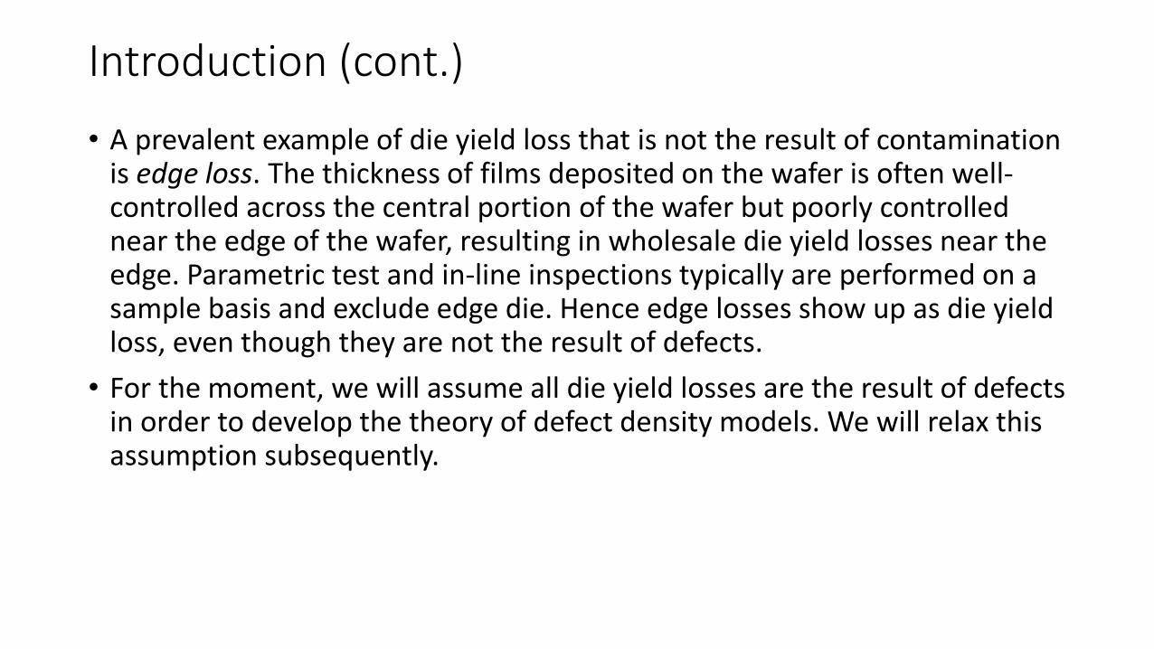
• A prevalent example of die yield loss that is not the result of contamination is edge loss. The thickness of films deposited on the wafer is often well-controlled across the central portion of the wafer but poorly controlled near the edge of the wafer, resulting in wholesale die yield losses near the edge. Parametric test and in-line inspections typically are performed on a sample basis and exclude edge die. Hence edge losses show up as die yield loss, even though they are not the result of defects.
• For the moment, we will assume all die yield losses are the result of defects in order to develop the theory of defect density models. We will relax this assumption subsequently.

The Poisson Model
• Suppose the mean number of defects per die is λ0. According to the Poisson probability distribution function, the probability that a die has kdefects is given by
• The probability the die works is P(0); the expected die yield is therefore
• If the mean defect density is D0 defects per square centimeter, and the die area is A sq cm, then we should take λ0 = D0A. We therefore write
• This is called the Poisson die yield model.
,2,1,0for ,!
)( 00
==−
kk
ekP
kλλ
.)0( 0λ−== ePDY
.0 ADeDY −=

The Poisson Model (cont.)
• Given an observed die yield DY for a product with die area A, we can infer that the underlying defect density in the fab is
• A very useful feature of the Poisson model is the additivity of defects. If the overall defect density D0 is decomposable into defectivity contributions at different steps or different mask layers, e.g.,
D0 = D1 + D2 + D3 + … + Dn ,then the yield loss contribution of each step or layer is easily identified, as the overall die yield has a product form:
.ln0 A
DYD −=
.1
10 ∏=
−−
− =∑
== =
n
i
ADDA
AD i
n
ii
eeeDY

The Poisson Model (cont.)
• Using this product form, one can calculate the yield improvement to be gained from reductions in defect density achieved at various steps or layers. For example, if the defect density in layer j is reduced from Dj to Dj –∆Dj, then the new die yield is
• Empirically, the Poisson yield model has been found to give accurate yield predictions for small die (when A ≤ 0.25 sq cm) and when the expected number of defects per die is low (when D0A ≪ 1.0). In the case of large die areas, it tends to underestimate die yield, for reasons that will be explained later. Nonetheless, in almost any situation, it is accurate for estimating small changes in die yield as a function of small changes in step-level or layer defect densities.
.1
DYeeeDY jij DAn
i
ADDANEW ∆
=
−∆ == ∏
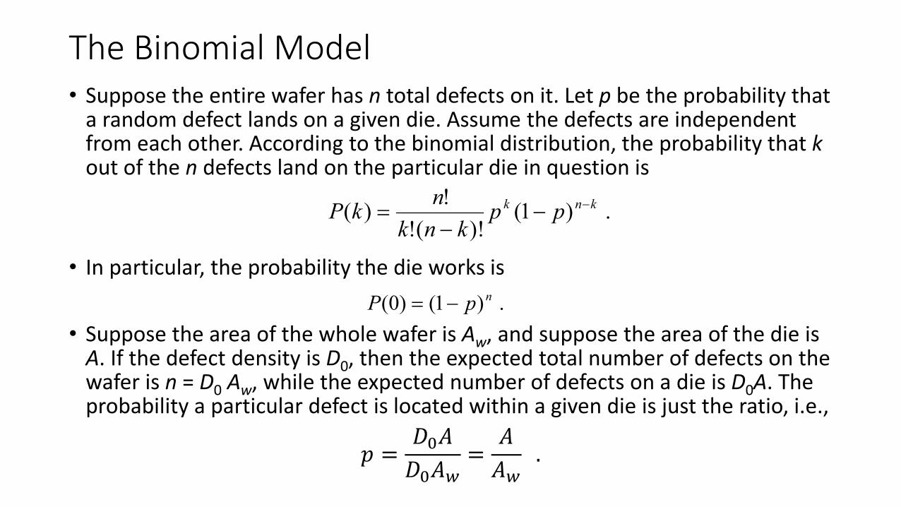
The Binomial Model• Suppose the entire wafer has n total defects on it. Let p be the probability that
a random defect lands on a given die. Assume the defects are independent from each other. According to the binomial distribution, the probability that kout of the n defects land on the particular die in question is
• In particular, the probability the die works is
• Suppose the area of the whole wafer is Aw, and suppose the area of the die is A. If the defect density is D0, then the expected total number of defects on the wafer is n = D0 Aw, while the expected number of defects on a die is D0A. The probability a particular defect is located within a given die is just the ratio, i.e.,
𝑝𝑝 =𝐷𝐷0𝐴𝐴𝐷𝐷0𝐴𝐴𝑤𝑤
=𝐴𝐴𝐴𝐴𝑤𝑤
.
.)1()!(!
!)( knk ppknk
nkP −−−
=
.)1()0( npP −=
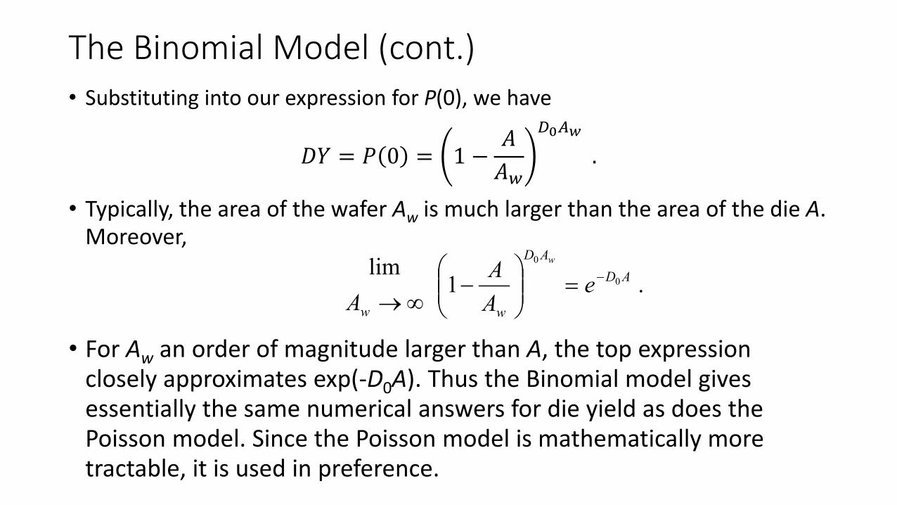
The Binomial Model (cont.)• Substituting into our expression for P(0), we have
𝐷𝐷𝐷𝐷 = 𝑃𝑃 0 = 1 −𝐴𝐴𝐴𝐴𝑤𝑤
𝐷𝐷0𝐴𝐴𝑤𝑤.
• Typically, the area of the wafer Aw is much larger than the area of the die A. Moreover,
• For Aw an order of magnitude larger than A, the top expression closely approximates exp(-D0A). Thus the Binomial model gives essentially the same numerical answers for die yield as does the Poisson model. Since the Poisson model is mathematically more tractable, it is used in preference.
.1lim
0
0
ADAD
ww
eAA
A
w
−=
−
∞→

Mixed Distribution Models• Actual data on defects shows that defect and particle densities vary widely
from chip to chip, from wafer to wafer, and even from lot to lot. In fact, the defects frequently tend to cluster together. Because of this, the Poisson model tends to underestimate die yield when the expected number of defects per chip is greater than one or when the die area is relatively large. (When the defects cluster together in some die, then other die can be relatively defect-free, thereby increasing the yield compared to the case when defects are more spread out.)
• One approach for dealing with this problem is to posit that the defect density D itself varies according to a probability distribution f(D). This was first done by B. T. Murphy of Bell Labs. The expected die yield in this case is expressed as
∫∞
−=0
.)( dDDfeDY DA

Mixed Distribution Models (cont.)• By definition, the distribution f(D) has mean D0, but beyond that, we don't
have much of an idea as to what it should look like. If one assumes D is distributed uniformly between 0 and 2D0, the previous integral expression simplifies to
• If one assumes D is distributed according to a symmetrical triangular distribution extending from 0 to 2D0 with peak at D0, it can be shown that the integral simplifies to
• This expression is commonly referred to as the Murphy model for die yield.Given a die yield DY and the chip area A, one can numerically solve for D0.
.2
1
0
2 0
ADeDY
AD−−=
.12
0
0
−=
−
ADeDY
AD

Mixed Distribution Models (cont.)• If one assumes D is distributed according to an exponential distribution,
i.e.,
it can be shown that the integral simplifies to
which is known as the Seeds model for die yield.
,1)( 0
0
DD
eD
Df−
=
,1
1
0ADDY
+=

Mixed Distribution Models (cont.)• A variant of the Seeds model, known as the Bose-Einstein model for die yield,
is a product form
where n is the number of critical mask layers. The idea behind the Bose-Einstein model is that most fatal defects are deposited in certain difficult (“critical”) mask layers. For example, metal layers are especially prone to the generation of fatal defects. We would expect that a device fabricated in a process technology with a given number of critical layers (say, four metal layers) will have a lower die yield than a device with the same area fabricated in another technology with fewer critical layers (say, two metal layers).
The Bose-Einstein model can be developed assuming die yield in each critical layer is expressed using the Seeds model, and overall die yield is the product of defect-limited yields in all the critical layers.
,1
10
n
ADDY
+
=

Mixed Distribution Models (cont.)• If f(D) is assumed to be a Gamma distribution, it has been shown that the
integral reduces to a Negative Binomial model, i.e.,
where α is called the cluster parameter. If defect data is available, this parameter can be estimated from the defect data as
Here, �̅�𝜆 is the mean number of defects per die and σ is the standard deviation of the number of defects per die.
,1 0α
α
−
+=
ADDY
( ) .2
2
λσλα
−=
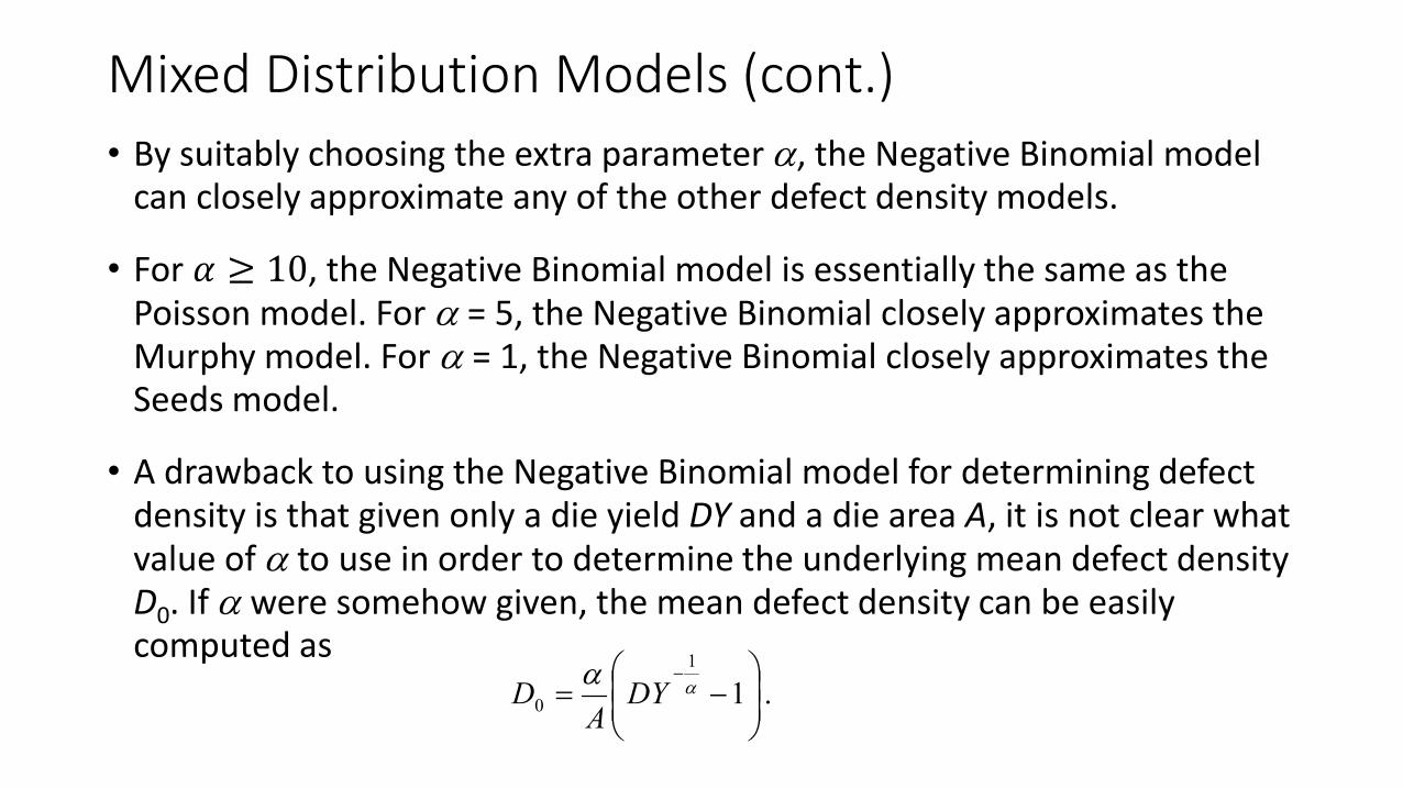
Mixed Distribution Models (cont.)• By suitably choosing the extra parameter α, the Negative Binomial model
can closely approximate any of the other defect density models.
• For 𝛼𝛼 ≥ 10, the Negative Binomial model is essentially the same as the Poisson model. For α = 5, the Negative Binomial closely approximates the Murphy model. For α = 1, the Negative Binomial closely approximates the Seeds model.
• A drawback to using the Negative Binomial model for determining defect density is that given only a die yield DY and a die area A, it is not clear what value of α to use in order to determine the underlying mean defect density D0. If α were somehow given, the mean defect density can be easily computed as
.11
0
−=
−αα DY
AD

Practical Defect Density Models• For small die sizes A ≤ 0.25 sq cm, or for low defect densities AD0 ≪ 1, the
simple Poisson model (2) is widely used and is accurate. Moreover, if one is only concerned about the change in die yield given a change in defect density at one or several process steps, an analysis using the Poisson model is sufficiently accurate.
• For large die sizes, the Negative Binomial model is the most flexible and potentially most accurate model. However, the extra parameter α needs to be determined by statistical methods or by estimation from actual defect data. Where such data are not available, the Murphy model is frequently used.

Models Incorporating Both Random and Systematic Yield Losses• Now suppose that in addition to random defects there are losses
independent of die size that we shall term systematic yield losses. We decompose overall die yield as DY = YSYR, where YR is the defect-limited yield and YS is the systematic-limited yield. If we posit a simple Poisson Model for defects, we have
• Using linear regression, we can determine a best fit of the two parameters YS and D0 to actual data on DY vs. A if we take logs of both sides of the above equation:
.0ADSRS eYYYDY −==
.lnln 0ADYDY S −=

Models With Random and Systematic Yield Losses (cont.)
• Here, ln YS is the constant and D0 is the coefficient on the independent variable A. If we had die yield data for many different-sized products produced in the same fab, we could compute least-squares regression estimates of ln Ys and D0.
• But suppose there is only one product being produced. As explained in following slides, we can determine these unknown parameters from wafer map data for the product using what is known as the windowing technique.
• A wafer map presents the yield by die position on the wafer. An example of a stacked wafer map, showing the average yield by die position for many wafers of the same product, is depicted in Figure 1.
.lnln 0ADYDY S −=

Figure 1. Sample Wafer Map

Models With Random and Systematic Yield Losses (cont.)• The windowing technique is explained as follows. The average die yield for
the product vs. the die area of the product constitutes one data point. Now suppose we group the dice printed across the wafer surface into pairs, and pretend that the pair is a single die with area 2A. This paired single-die only works if both component dice work. From review of the wafer map, the die yield of this paired single-die can be identified. This provides a second data point. The procedure can be repeated for die groups of size 3, 4, 5, 6, 7, 8, etc., providing more data points for the regression.
• Just as for the simple Poisson model for defect density, any of the compound defect density models could be appended with a systematic-limited yield coefficient YS. In practice, a two-parameter model such as the simple Poisson with a systematic-limited yield coefficient is typically sufficient for practical purposes.

Models With Random and Systematic Yield Losses (cont.)• We remark that the windowing technique simply sorts out yield losses into
those that are independent of die area versus those that are dependent on die area. This is not equivalent to a decomposition of yield losses by point-defect mechanisms vs. systematic mechanisms. For example, edge losses will be larger for wafers with larger-sized dice printed on them than for wafers with small dice. Thus losses from some of the non-defect mechanisms such as edge loss would end up being accounted for in the D0parameter rather than in the YS parameter.
• So to sort out truly random defect losses from losses stemming from systematic mechanisms, we need a different approach …

Models With Baseline Random and Systematic Yield Losses • A different and useful decomposition of die yield stems from an SPC-type
viewpoint. Suppose we posit that the truly random die yield losses all must come from a stable, stationary system of chance causes that we classify as baseline defects.
• There may be occasional excursions (significant additional yield losses from this baseline) when the process or equipment drifts out of control, either misprocessing or depositing excessive particles. Losses from such excursions, as well as chronic losses that are not randomly distributed, are termed systematic yield losses.
• Systematic yield losses have an observable signature. It could be a signature over time (e.g., one or several lots with exceptionally poor yields), or a spatial signature (e.g., certain die positions on the wafer or certain wafer positions within the lot with much lower-than-average yields). Edge loss is a good example of a systematic yield loss with a spatial signature.

Models With Baseline Random and Systematic Yield Losses (cont.) • Suppose we abstractly collect all systematic losses into a single term 1-YS
and all random losses into a single term 1-YR. (YS is known as the systematic limited yield, YR is the baseline defect-limited yield.) The overall die yield is DY = YRYS.
• Improvement of baseline yield requires fundamental improvement in the cleanliness of the process and equipment.
• Improvement of systematic yield requires improved process execution and/or improved process monitoring and control (to detect excursions from baseline losses and react to contain losses from such excursions).
• Typically, faster progress in yield improvement can be made on the systematic side, whereby signatures can be analyzed to help determine root causes and to help devise and carry out engineering projects to mitigate specific systematic yield losses.

Models With Baseline Random and Systematic Yield Losses (cont.) • It is therefore helpful to know the YR vs. YS breakdown of overall die yield,
as well as the breakdown of 1-YS into its many component losses.
• Some insight for the decomposition of yield into YR and YS components may be gained by viewing a wafer yield histogram in addition to the wafer yield map. An example wafer yield histogram is presented in Figure 2. From a large sample of wafers, the number of good die per wafer vs. the number of wafers achieving that yield is plotted.

0
10
20
30
40
50
60
No.
of w
afer
s
Yield (%)
Figure 2. Example of Yield Histogram
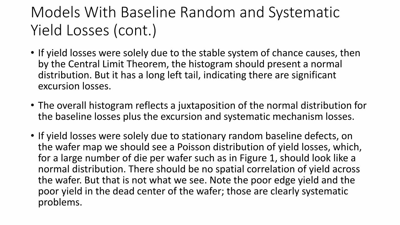
Models With Baseline Random and Systematic Yield Losses (cont.) • If yield losses were solely due to the stable system of chance causes, then
by the Central Limit Theorem, the histogram should present a normal distribution. But it has a long left tail, indicating there are significant excursion losses.
• The overall histogram reflects a juxtaposition of the normal distribution for the baseline losses plus the excursion and systematic mechanism losses.
• If yield losses were solely due to stationary random baseline defects, on the wafer map we should see a Poisson distribution of yield losses, which, for a large number of die per wafer such as in Figure 1, should look like a normal distribution. There should be no spatial correlation of yield across the wafer. But that is not what we see. Note the poor edge yield and the poor yield in the dead center of the wafer; those are clearly systematic problems.

Figure 1. Sample Wafer Map

Models With Baseline Random and Systematic Yield Losses (cont.) • Suppose we looked at a wafer map developed solely from wafers that to the best
of our knowledge were not involved in any excursions. Suppose we focus on the best-observed-yielding die site in that map, probably located near the center of this wafer map. We will certainly ignore the die sites near the edge that exhibit edge losses, and we will ignore the poor-yielding die site in the center of the map in Figure 1, as well as any other die sites exhibiting a spatial signature. In Figure 1, the best-yielding die site exhibits a die yield of 54%, and there is only one die site achieving this yield.
• For baseline random defects, die yield is well-characterized by a Binomial distribution. (Recall that a Poisson model and a Binomial model are equivalent when the number of die per wafer is sufficiently large.) For Binomial die yield, the distribution exhibited by the wafer histogram should be a normal distribution, if the wafer sample is sufficiently large. For such a distribution, a span of 6σ should contain (almost) all observations and the peak should be centered 3σ from the maximum die yield.

Models With Baseline Random and Systematic Yield Losses (cont.) • The overall yield distribution as seen in Figure 2 is a juxtaposition of the
baseline random defect-limited yield and the systematic mechanisms-limited yield. We might expect that excursions add a long left-hand tail, while chronic systematic losses (such as edge losses) shift some of the distribution to the left.
• We can argue that the only time the best-observed yield is achieved is when no systematic losses are present and we are witnessing a point that is at the right-hand edge of the (unseen) normal distribution for the baseline random yield. We therefore could expect the distance between the mean of the baseline random yield distribution and the maximum die yield identified on a stacked wafer map to be approximately 3σ of the distribution that results from the baseline random defect-limited yield, as long as the number of die per wafer is sufficiently large. We can use this observation to estimate YR as follows.

Models With Baseline Random and Systematic Yield Losses (cont.) • For a Binomial model with mean YR, the standard deviation of the average
yield is given by
where m is the total number of wafers in the stack. Let MY denote the maximum die yield that is observed. The difference between MY and the unknown YR depends on the number of die sites that were considered and at how many die sites MY was observed. For example, suppose there were 300 die sites considered (die sites subject to edge loss or other chronic systematic loss mechanisms are ignored), and suppose MY was observed at 2die sites. Using a normal approximation, that would suggest MY occurred at Φ -1(1-2/300) standard deviations above YR where Φ denotes the cumulative standard normal density function.
mYY RR /)1( −=σ

Models With Baseline Random and Systematic Yield Losses (cont.) • More generally, if we apply the normal approximation so that the distance from
YR to MY is Φ -1(1 – l/n)σ, where l is the number of instances MY appears on the stacked wafer map and n is the number of die sites considered on the stacked wafer map, then we estimate MY occurs at YR + kσ where k = Φ -1(1 – l/n)σ.
• In particular, if MY were observed at 2 out of 88 die sites, that would suggest that MY is two standard deviations above YR, and if MY were observed at 1 out of 714 die sites, that would suggest that MY is three standard deviations above YR.
• Using this approximation, we have
which may be solved using the quadratic formula to find YR. Once YR is determined, we can divide it into DY to determine YS .
mYYnlkYMY RRR /)1()/1(1 −−Φ==− −σ

Models With Baseline Random and Systematic Yield Losses (cont.) • This binomial-sigma method will result in a smaller systematic mechanism
limited yield than the YS term computed using the windowing method.
• The virtue of this approach to match maximum-observed-yield is that edge losses and defect excursions are excluded from the determination of YR (to the extent that they do not contribute to the die sites exhibiting maximum yield).
• That is, defect losses are sorted out into baseline losses present across all die sites on every wafer vs. other losses with a spatial or temporal signature.

Figure 1. Sample Wafer Map

Models With Baseline Random and Systematic Yield Losses (cont.) • As an example, the wafer map in Figure 1 provided the average yields by
die site over a large group of wafers, in this case, 755 wafers.
• As for candidate die sites, we ignore the top three rows of dice, seemingly subject to some systematic mechanism. Starting in the fourth row and ignoring the edge die subject to edge loss, we have one row of 15, one row of 17, two rows of 19, then 10 rows of 21, 2 rows of 19, one row of 17, one row of 15, one row of 13, and one row of 9, ignoring the bottom row subject to edge loss. This makes for a total of 372 candidate die sites for observing the maximum die yield.
• The maximum observed die yield is 57%, occurring at only one site out of the 372 candidate die sites. Then k = Φ -1(1 – 1/372) = 2.78. Solving the quadratic equation, we obtain the estimate YR = 51.8%. The average die yield is 43.1%, implying YS = 83.2%.