Embed Size (px)
Citation preview
Concepts of Optimizing Power Semiconductor Devices Using Novel Nano-Structure for Low Losses 209
Concepts of Optimizing Power Semiconductor Devices Using Novel Nano-Structure for Low Losses
Ye, Hua and Haldar, Pradeep
x
Concepts of Optimizing Power Semiconductor Devices Using Novel
Nano-Structure for Low Losses
Ye, Hua1 and Haldar, Pradeep2 1Microsoft Corporation
2College of Nanoscale Science and Engineering State University of New York at Albany
USA
1. Introduction
In the chapter, the authors discuss two new concepts of optimizing power devices that directly addressing the limitations of current IGBT (Insulated Gate Bipolor Transistors) and SJ (Superjunction) MOSFET technologies. Power MOSFETs and IGBTs are the two main competing power semiconductor devices for switching electric power in electrical power conversion systems at mid-voltage ratings. Power MOSFETs conduct current as soon as a forward bias voltage is applied between the drain and the source electrodes; however, as the blocking voltage capability increases, the on-resistance of conventional power MOSFETs increases proportionally to the second order of its blocking voltage (Hu, 1979). In order to overcome the limitation of conventional power MOSFET, IGBT is introduced. Unlike conventional power MOSFET, the forward voltage drop of IGBTs does not follow a second order dependence on blocking voltage because the conductivity of the voltage blocking drift layer can modulated by carrier injection during forward bias. However, IGBTs cannot carry any significant current until the external bias surpasses an internal barrier voltage (heel voltage). This distinction, among other considerations, makes the selection of power semiconductor switches a trade-off between MOSFETs and IGBTs. For instance, paralleling IGBTs will not reduce the heel voltage. Another technology to address the limitation of conventional power MOSFET is SJ MOSFET that employs the charge compensation concept have been significantly researched in an effort to break the “silicon limit” and led to growing commercialization (Coe, 1988; Chen, 1993; Fujihira, 1997; Shenoy, et al., 1999; Deboy, et al., 1998). These devices use an alternating p and n charge compensation structure to replace the planar voltage-blocking drift layer in the conventional power MOSFET, where the n-columns can be much more heavily doped than the planar drift layer, leading to significant reduction in specific on-resistance. The breakdown voltage of an SJ MOSFET is proportional to the depth of the p and n columns. At the same time, reducing the widths of the alternating p and n columns leads to higher allowable doping levels and thus smaller on-resistance (Fujihira, 1997). However, fabricating the SJ structure with increasing depths of p and n columns and decreasing
9
www.intechopen.com
Semiconductor Technologies210
column sizes leads to increasing process difficulties. In addition, the criticality of match the doping levels in the p and n regions with their widths on the breakdown voltage further increases the process difficulties (Shenoy, et al., 1999). State-of-the-art fabrication techniques -- such as high-energy implantation, multi-epitaxial growth, and trench-filling -- have been demonstrated to be only sufficient to create low to mid voltage range (<1000V) devices (Deboy, et al., 1998; Miura, et al., 2005; von Borany, et al., 2004; Rub, et al., 2004; Onishi, et al., 2002; Minato, et al., 2000; Rochefort, et al., 2002; Saito, et al., 2005; Liang, et al., 2001; Chen & Liang, 2007; Gan, et al., 2001; ). The first concept discussed in this chapter is a proposal of a mid-to-high voltage power switch that utilizes reverse band-to-band tunneling and an avalanche injection mechanism called Tunnelling Junction Enhanced MOSFET (TJE-MOSFET) (Ye & Haldar, 2008). This device is predicted to have the best properties of both power MOSFETs and IGBTs (Insulated Gate Bipolar Transistors) - the two main competing power semiconductor technologies at mid-voltage (500-1000V) ratings. The structure and the operating mechanism of the TJE-MOSFET are described. The proposed novel device operates in a way similar to an IGBT; however, due to the inclusion of a nano-structured band-to-band tunneling junction, the internal barrier voltage for forward conduction is much smaller than that in an IGBT. Numerical simulation suggests that, at the same current level, the forward voltage drop of the TJE-MOSFET is much smaller than that of an IGBT. Compared to power MOSFETs, the new device has a lower forward voltage drop even at very low current levels. The second concept is a novel SJ MOSFET fabrication process based on porous silicon formation (Ye & Haldar, 2008). The voltage blocking SJ structure is directly created within the lightly doped thin silicon wafer instead of growing the costly thick epitaxial layer. The charge compensating structures are created by etching the structured macro-pores, followed by passivating the walls and filling the pores with oppositely charged poly-silicon. The effects of charge imbalance and the thickness of the passivation layer are studied by physics-based numerical device simulations. It is found that even with some amount of charge imbalance, the proposed method can still produce high-voltage MOSFETs with much better performance than existing technology. A thick oxide layer between the p and n columns is found to be helpful in alleviating the JFET (Junction-Field-Effect Transitor) effect when the doping concentrations in the p and n columns are low in comparison with a conventional SJ structure. The inclusion of an oxide layer between the p and n columns is found to help increase the device efficiency in addition to its ability to prevent dopant interdiffusion.
2. Tunnelling Junction Enhanced MOSFET (TJE-MOSFET)
2.1 Background A band-to-band tunneling junction diode working in the forward bias regime has been widely used in a variety of the applications such as switching, oscillation, and amplification by taking advantage of its negative resistance characteristics. Reverse-biased tunneling has received much less attention until recently. A few attempts of taking advantage of reverse band-to-band tunneling breakdown in order to create a new family of transistors that aims at replacing the today’s CMOS technology have been reported recently (Aydin, et al., 2004). In addition, reverse band-to-band tunneling is also found to be important in CMOS at room temperature for dopant concentrations above 17 35 10 cm , which presents a limit to scaling of future CMOS technology (Solomon, et al, 2004). Solomon et al. (Solomon, et al, 2004) have
studied ion-implanted p/n junction diodes with doping levels up to 1020 cm-3 by measuring current-voltage characteristics in both forward and reverse bias conditions. Their measurements show that for a highly doped p/n junction diode, very high current densities are achieved at very low reverse bias voltage, which is dominated by band-to-band tunneling. They conclude that the higher the junction doping concentration, the smaller the effective tunneling distance, resulting in higher tunneling current densities. In this section, a novel power switch is proposed, which utilizes a reverse biased nanoscale band-to-band tunneling structure in order to reduce the forward voltage drop during conduction. The device structure and the operating mechanism are described. The proposed TJE-MOSFET operates in a way similar to an IGBT. However, by taking advantage of a reverse-biased band-to-band tunneling junction, the internal barrier voltage for forward conduction is much smaller than that of an IGBT. Numerical simulation suggests that, at the same current level, the forward voltage drop of the TJE-MOSFET is much smaller than that of an IGBT. Compared to power MOSFETs (conventional as well as the superjunction MSOFETs), the TJE-MOSFET has a much lower forward voltage drop even at very low current levels.
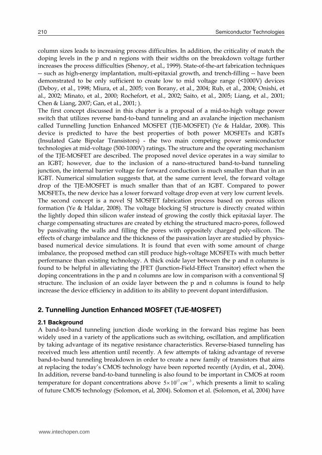
2.2 Structure and Operation Mechanism of the Device The structure of the TJE-MOSFET is very similar to that of a power MOSFET or IGBT as shown in Figure 1(a-c), where they all share a similar gate structure. They all feature a lightly-doped n- drift layer which is used to block the high voltage during the OFF-state when the junction between this layer and the p-base layer (J2) is reverse biased. The differences are at the back side of the devices. Compared to power MOSFETs and IGBTs, the TJE-MOSFET features a unique sharp (abrupt) and highly doped p++/n++ junction J1. The doping levels in the p++ and n++ layer are on the orders of 3 x 10¹⁹ to 1 x 1021 cm-3. The p++ layer has to be very thin with thickness on the order of several to several tens of nanometers. An optional n layer several microns thick with mid-level doping can be included as a minority carrier injection buffer layer and/or field-stop layer if a punch-through design is desired. The operation of the device is similar to a power MOSFET or IGBT in that the ON and the OFF states of the device are controlled by altering the bias voltage at the gate electrode.
n++
p+p base (3e17)
n++
p++
n- drift (~1e14)
junction J1
junction J2
Gate electrode Source electrode
Drain electrode
channel
e-
e-
e-
h+
h+
h+
n buffer
n++
p+p base
n++
n- drift
Gate electrode Source electrode
Drain electrode
channel
e-
Band-to-band tunnelingand carrier injection
n++
p+p base
p+
n- drift
Gate electrode Emitter electrode
Collector electrode
channel
e-
n buffer
(a) (b) (c) Fig. 1 (a) Structure of the device; (b) power MOSFET; (c) IGBT During the forward conduction mode or switch-on, the channels near the gate oxide in the p-base region are created by applying a positive gate-to-source bias voltage above the gate
www.intechopen.com
Concepts of Optimizing Power Semiconductor Devices Using Novel Nano-Structure for Low Losses 211
column sizes leads to increasing process difficulties. In addition, the criticality of match the doping levels in the p and n regions with their widths on the breakdown voltage further increases the process difficulties (Shenoy, et al., 1999). State-of-the-art fabrication techniques -- such as high-energy implantation, multi-epitaxial growth, and trench-filling -- have been demonstrated to be only sufficient to create low to mid voltage range (<1000V) devices (Deboy, et al., 1998; Miura, et al., 2005; von Borany, et al., 2004; Rub, et al., 2004; Onishi, et al., 2002; Minato, et al., 2000; Rochefort, et al., 2002; Saito, et al., 2005; Liang, et al., 2001; Chen & Liang, 2007; Gan, et al., 2001; ). The first concept discussed in this chapter is a proposal of a mid-to-high voltage power switch that utilizes reverse band-to-band tunneling and an avalanche injection mechanism called Tunnelling Junction Enhanced MOSFET (TJE-MOSFET) (Ye & Haldar, 2008). This device is predicted to have the best properties of both power MOSFETs and IGBTs (Insulated Gate Bipolar Transistors) - the two main competing power semiconductor technologies at mid-voltage (500-1000V) ratings. The structure and the operating mechanism of the TJE-MOSFET are described. The proposed novel device operates in a way similar to an IGBT; however, due to the inclusion of a nano-structured band-to-band tunneling junction, the internal barrier voltage for forward conduction is much smaller than that in an IGBT. Numerical simulation suggests that, at the same current level, the forward voltage drop of the TJE-MOSFET is much smaller than that of an IGBT. Compared to power MOSFETs, the new device has a lower forward voltage drop even at very low current levels. The second concept is a novel SJ MOSFET fabrication process based on porous silicon formation (Ye & Haldar, 2008). The voltage blocking SJ structure is directly created within the lightly doped thin silicon wafer instead of growing the costly thick epitaxial layer. The charge compensating structures are created by etching the structured macro-pores, followed by passivating the walls and filling the pores with oppositely charged poly-silicon. The effects of charge imbalance and the thickness of the passivation layer are studied by physics-based numerical device simulations. It is found that even with some amount of charge imbalance, the proposed method can still produce high-voltage MOSFETs with much better performance than existing technology. A thick oxide layer between the p and n columns is found to be helpful in alleviating the JFET (Junction-Field-Effect Transitor) effect when the doping concentrations in the p and n columns are low in comparison with a conventional SJ structure. The inclusion of an oxide layer between the p and n columns is found to help increase the device efficiency in addition to its ability to prevent dopant interdiffusion.
2. Tunnelling Junction Enhanced MOSFET (TJE-MOSFET)
2.1 Background A band-to-band tunneling junction diode working in the forward bias regime has been widely used in a variety of the applications such as switching, oscillation, and amplification by taking advantage of its negative resistance characteristics. Reverse-biased tunneling has received much less attention until recently. A few attempts of taking advantage of reverse band-to-band tunneling breakdown in order to create a new family of transistors that aims at replacing the today’s CMOS technology have been reported recently (Aydin, et al., 2004). In addition, reverse band-to-band tunneling is also found to be important in CMOS at room temperature for dopant concentrations above 17 35 10 cm , which presents a limit to scaling of future CMOS technology (Solomon, et al, 2004). Solomon et al. (Solomon, et al, 2004) have
studied ion-implanted p/n junction diodes with doping levels up to 1020 cm-3 by measuring current-voltage characteristics in both forward and reverse bias conditions. Their measurements show that for a highly doped p/n junction diode, very high current densities are achieved at very low reverse bias voltage, which is dominated by band-to-band tunneling. They conclude that the higher the junction doping concentration, the smaller the effective tunneling distance, resulting in higher tunneling current densities. In this section, a novel power switch is proposed, which utilizes a reverse biased nanoscale band-to-band tunneling structure in order to reduce the forward voltage drop during conduction. The device structure and the operating mechanism are described. The proposed TJE-MOSFET operates in a way similar to an IGBT. However, by taking advantage of a reverse-biased band-to-band tunneling junction, the internal barrier voltage for forward conduction is much smaller than that of an IGBT. Numerical simulation suggests that, at the same current level, the forward voltage drop of the TJE-MOSFET is much smaller than that of an IGBT. Compared to power MOSFETs (conventional as well as the superjunction MSOFETs), the TJE-MOSFET has a much lower forward voltage drop even at very low current levels.
2.2 Structure and Operation Mechanism of the Device The structure of the TJE-MOSFET is very similar to that of a power MOSFET or IGBT as shown in Figure 1(a-c), where they all share a similar gate structure. They all feature a lightly-doped n- drift layer which is used to block the high voltage during the OFF-state when the junction between this layer and the p-base layer (J2) is reverse biased. The differences are at the back side of the devices. Compared to power MOSFETs and IGBTs, the TJE-MOSFET features a unique sharp (abrupt) and highly doped p++/n++ junction J1. The doping levels in the p++ and n++ layer are on the orders of 3 x 10¹⁹ to 1 x 1021 cm-3. The p++ layer has to be very thin with thickness on the order of several to several tens of nanometers. An optional n layer several microns thick with mid-level doping can be included as a minority carrier injection buffer layer and/or field-stop layer if a punch-through design is desired. The operation of the device is similar to a power MOSFET or IGBT in that the ON and the OFF states of the device are controlled by altering the bias voltage at the gate electrode.
n++
p+p base (3e17)
n++
p++
n- drift (~1e14)
junction J1
junction J2
Gate electrode Source electrode
Drain electrode
channel
e-
e-
e-
h+
h+
h+
n buffer
n++
p+p base
n++
n- drift
Gate electrode Source electrode
Drain electrode
channel
e-
Band-to-band tunnelingand carrier injection
n++
p+p base
p+
n- drift
Gate electrode Emitter electrode
Collector electrode
channel
e-
n buffer
(a) (b) (c) Fig. 1 (a) Structure of the device; (b) power MOSFET; (c) IGBT During the forward conduction mode or switch-on, the channels near the gate oxide in the p-base region are created by applying a positive gate-to-source bias voltage above the gate
www.intechopen.com
Semiconductor Technologies212
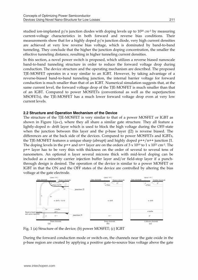
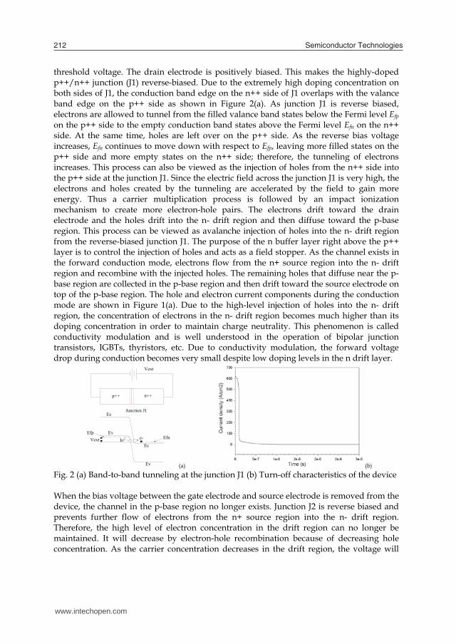
threshold voltage. The drain electrode is positively biased. This makes the highly-doped p++/n++ junction (J1) reverse-biased. Due to the extremely high doping concentration on both sides of J1, the conduction band edge on the n++ side of J1 overlaps with the valance band edge on the p++ side as shown in Figure 2(a). As junction J1 is reverse biased, electrons are allowed to tunnel from the filled valance band states below the Fermi level Efp on the p++ side to the empty conduction band states above the Fermi level Efn on the n++ side. At the same time, holes are left over on the p++ side. As the reverse bias voltage increases, Efn continues to move down with respect to Efp, leaving more filled states on the p++ side and more empty states on the n++ side; therefore, the tunneling of electrons increases. This process can also be viewed as the injection of holes from the n++ side into the p++ side at the junction J1. Since the electric field across the junction J1 is very high, the electrons and holes created by the tunneling are accelerated by the field to gain more energy. Thus a carrier multiplication process is followed by an impact ionization mechanism to create more electron-hole pairs. The electrons drift toward the drain electrode and the holes drift into the n- drift region and then diffuse toward the p-base region. This process can be viewed as avalanche injection of holes into the n- drift region from the reverse-biased junction J1. The purpose of the n buffer layer right above the p++ layer is to control the injection of holes and acts as a field stopper. As the channel exists in the forward conduction mode, electrons flow from the n+ source region into the n- drift region and recombine with the injected holes. The remaining holes that diffuse near the p-base region are collected in the p-base region and then drift toward the source electrode on top of the p-base region. The hole and electron current components during the conduction mode are shown in Figure 1(a). Due to the high-level injection of holes into the n- drift region, the concentration of electrons in the n- drift region becomes much higher than its doping concentration in order to maintain charge neutrality. This phenomenon is called conductivity modulation and is well understood in the operation of bipolar junction transistors, IGBTs, thyristors, etc. Due to conductivity modulation, the forward voltage drop during conduction becomes very small despite low doping levels in the n drift layer.
n++p++
Junction J1
Vext
Vext
Ec
EvEfp
Ec
Ev
Efne-h+
(a) (b)
Fig. 2 (a) Band-to-band tunneling at the junction J1 (b) Turn-off characteristics of the device When the bias voltage between the gate electrode and source electrode is removed from the device, the channel in the p-base region no longer exists. Junction J2 is reverse biased and prevents further flow of electrons from the n+ source region into the n- drift region. Therefore, the high level of electron concentration in the drift region can no longer be maintained. It will decrease by electron-hole recombination because of decreasing hole concentration. As the carrier concentration decreases in the drift region, the voltage will
gradually build up at the reverse biased junction J2, and this junction will sustain all the applied OFF-state voltage. The decrease of the forward current follows a similar pattern to the turn-off operation of IGBTs. As the gate voltage reduces below the gate threshold voltage, the electron current component will suddenly decrease to zero leading to a sharp drop of total current. However, current continues to flow through the device due to the high hole concentration in the n- drift region. This current gradually decreases as the hole concentration in the n- drift region gradually decreases by electron-hole recombination. The turn-off curve is illustrated in Figure 2(b) as obtained from numerical simulation that is described in the next section. Unlike an IGBT, where high-level injection occurs only when the applied voltage across the p/n junction near the collector electrode increases above the internal barrier of the junction (0.7V at room temperature), high-level injection in the TJE-MOSFET can happen at much smaller forward bias. Numerical simulations suggest that a much smaller forward voltage drop can be realized in the device when compared to an IGBT with the same current density level. Simulations also suggest that the forward voltage drop decreases with increasing doping concentration at the p++/n++ junction J1.
2.2 Numerical Simulation and Discussion
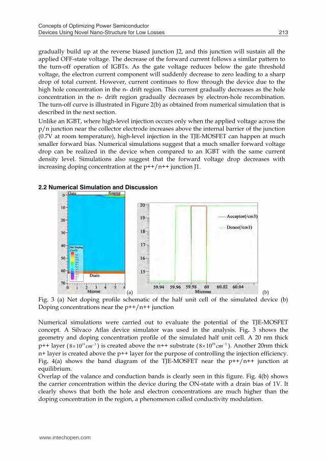
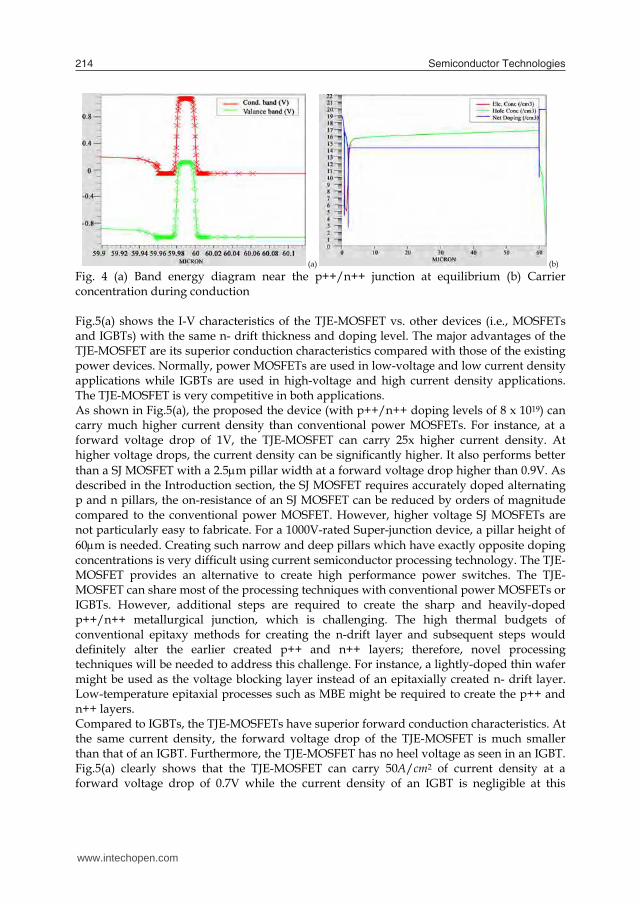
(a) (b) Fig. 3 (a) Net doping profile schematic of the half unit cell of the simulated device (b) Doping concentrations near the p++/n++ junction Numerical simulations were carried out to evaluate the potential of the TJE-MOSFET concept. A Silvaco Atlas device simulator was used in the analysis. Fig. 3 shows the geometry and doping concentration profile of the simulated half unit cell. A 20 nm thick p++ layer ( 19 38 10 cm ) is created above the n++ substrate ( 19 38 10 cm ). Another 20nm thick n+ layer is created above the p++ layer for the purpose of controlling the injection efficiency. Fig. 4(a) shows the band diagram of the TJE-MOSFET near the p++/n++ junction at equilibrium. Overlap of the valance and conduction bands is clearly seen in this figure. Fig. 4(b) shows the carrier concentration within the device during the ON-state with a drain bias of 1V. It clearly shows that both the hole and electron concentrations are much higher than the doping concentration in the region, a phenomenon called conductivity modulation.
www.intechopen.com
Concepts of Optimizing Power Semiconductor Devices Using Novel Nano-Structure for Low Losses 213
threshold voltage. The drain electrode is positively biased. This makes the highly-doped p++/n++ junction (J1) reverse-biased. Due to the extremely high doping concentration on both sides of J1, the conduction band edge on the n++ side of J1 overlaps with the valance band edge on the p++ side as shown in Figure 2(a). As junction J1 is reverse biased, electrons are allowed to tunnel from the filled valance band states below the Fermi level Efp on the p++ side to the empty conduction band states above the Fermi level Efn on the n++ side. At the same time, holes are left over on the p++ side. As the reverse bias voltage increases, Efn continues to move down with respect to Efp, leaving more filled states on the p++ side and more empty states on the n++ side; therefore, the tunneling of electrons increases. This process can also be viewed as the injection of holes from the n++ side into the p++ side at the junction J1. Since the electric field across the junction J1 is very high, the electrons and holes created by the tunneling are accelerated by the field to gain more energy. Thus a carrier multiplication process is followed by an impact ionization mechanism to create more electron-hole pairs. The electrons drift toward the drain electrode and the holes drift into the n- drift region and then diffuse toward the p-base region. This process can be viewed as avalanche injection of holes into the n- drift region from the reverse-biased junction J1. The purpose of the n buffer layer right above the p++ layer is to control the injection of holes and acts as a field stopper. As the channel exists in the forward conduction mode, electrons flow from the n+ source region into the n- drift region and recombine with the injected holes. The remaining holes that diffuse near the p-base region are collected in the p-base region and then drift toward the source electrode on top of the p-base region. The hole and electron current components during the conduction mode are shown in Figure 1(a). Due to the high-level injection of holes into the n- drift region, the concentration of electrons in the n- drift region becomes much higher than its doping concentration in order to maintain charge neutrality. This phenomenon is called conductivity modulation and is well understood in the operation of bipolar junction transistors, IGBTs, thyristors, etc. Due to conductivity modulation, the forward voltage drop during conduction becomes very small despite low doping levels in the n drift layer.
n++p++
Junction J1
Vext
Vext
Ec
EvEfp
Ec
Ev
Efne-h+
(a) (b)
Fig. 2 (a) Band-to-band tunneling at the junction J1 (b) Turn-off characteristics of the device When the bias voltage between the gate electrode and source electrode is removed from the device, the channel in the p-base region no longer exists. Junction J2 is reverse biased and prevents further flow of electrons from the n+ source region into the n- drift region. Therefore, the high level of electron concentration in the drift region can no longer be maintained. It will decrease by electron-hole recombination because of decreasing hole concentration. As the carrier concentration decreases in the drift region, the voltage will
gradually build up at the reverse biased junction J2, and this junction will sustain all the applied OFF-state voltage. The decrease of the forward current follows a similar pattern to the turn-off operation of IGBTs. As the gate voltage reduces below the gate threshold voltage, the electron current component will suddenly decrease to zero leading to a sharp drop of total current. However, current continues to flow through the device due to the high hole concentration in the n- drift region. This current gradually decreases as the hole concentration in the n- drift region gradually decreases by electron-hole recombination. The turn-off curve is illustrated in Figure 2(b) as obtained from numerical simulation that is described in the next section. Unlike an IGBT, where high-level injection occurs only when the applied voltage across the p/n junction near the collector electrode increases above the internal barrier of the junction (0.7V at room temperature), high-level injection in the TJE-MOSFET can happen at much smaller forward bias. Numerical simulations suggest that a much smaller forward voltage drop can be realized in the device when compared to an IGBT with the same current density level. Simulations also suggest that the forward voltage drop decreases with increasing doping concentration at the p++/n++ junction J1.
2.2 Numerical Simulation and Discussion
(a) (b) Fig. 3 (a) Net doping profile schematic of the half unit cell of the simulated device (b) Doping concentrations near the p++/n++ junction Numerical simulations were carried out to evaluate the potential of the TJE-MOSFET concept. A Silvaco Atlas device simulator was used in the analysis. Fig. 3 shows the geometry and doping concentration profile of the simulated half unit cell. A 20 nm thick p++ layer ( 19 38 10 cm ) is created above the n++ substrate ( 19 38 10 cm ). Another 20nm thick n+ layer is created above the p++ layer for the purpose of controlling the injection efficiency. Fig. 4(a) shows the band diagram of the TJE-MOSFET near the p++/n++ junction at equilibrium. Overlap of the valance and conduction bands is clearly seen in this figure. Fig. 4(b) shows the carrier concentration within the device during the ON-state with a drain bias of 1V. It clearly shows that both the hole and electron concentrations are much higher than the doping concentration in the region, a phenomenon called conductivity modulation.
www.intechopen.com
Semiconductor Technologies214
(a) (b)
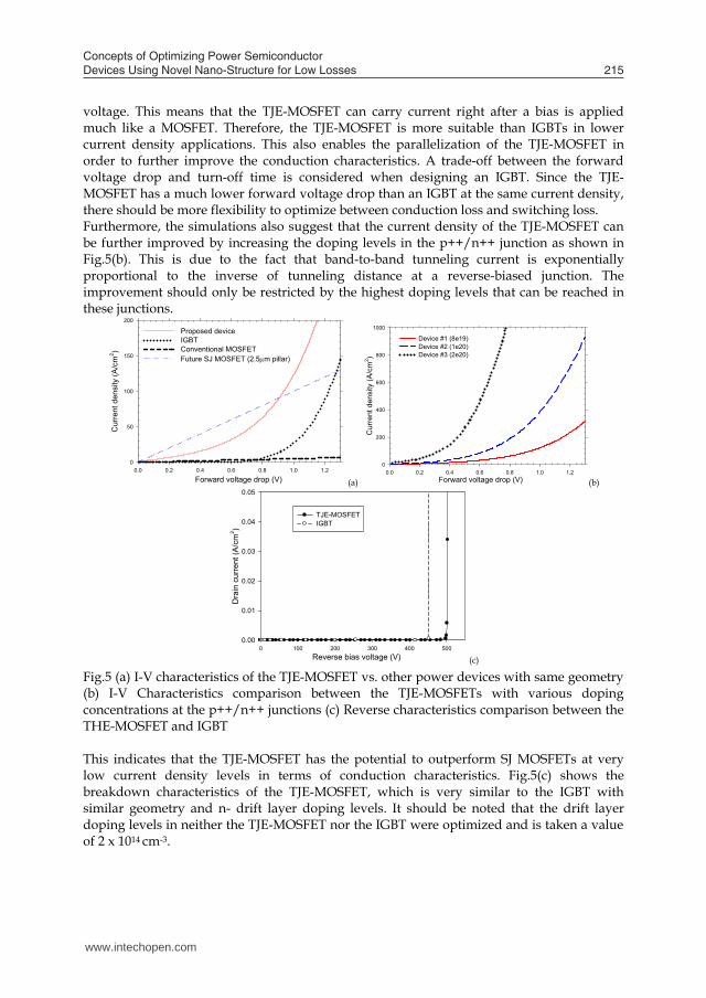
Fig. 4 (a) Band energy diagram near the p++/n++ junction at equilibrium (b) Carrier concentration during conduction Fig.5(a) shows the I-V characteristics of the TJE-MOSFET vs. other devices (i.e., MOSFETs and IGBTs) with the same n- drift thickness and doping level. The major advantages of the TJE-MOSFET are its superior conduction characteristics compared with those of the existing power devices. Normally, power MOSFETs are used in low-voltage and low current density applications while IGBTs are used in high-voltage and high current density applications. The TJE-MOSFET is very competitive in both applications. As shown in Fig.5(a), the proposed the device (with p++/n++ doping levels of 8 x 10¹⁹) can carry much higher current density than conventional power MOSFETs. For instance, at a forward voltage drop of 1V, the TJE-MOSFET can carry 25x higher current density. At higher voltage drops, the current density can be significantly higher. It also performs better than a SJ MOSFET with a 2.5m pillar width at a forward voltage drop higher than 0.9V. As described in the Introduction section, the SJ MOSFET requires accurately doped alternating p and n pillars, the on-resistance of an SJ MOSFET can be reduced by orders of magnitude compared to the conventional power MOSFET. However, higher voltage SJ MOSFETs are not particularly easy to fabricate. For a 1000V-rated Super-junction device, a pillar height of 60m is needed. Creating such narrow and deep pillars which have exactly opposite doping concentrations is very difficult using current semiconductor processing technology. The TJE-MOSFET provides an alternative to create high performance power switches. The TJE-MOSFET can share most of the processing techniques with conventional power MOSFETs or IGBTs. However, additional steps are required to create the sharp and heavily-doped p++/n++ metallurgical junction, which is challenging. The high thermal budgets of conventional epitaxy methods for creating the n-drift layer and subsequent steps would definitely alter the earlier created p++ and n++ layers; therefore, novel processing techniques will be needed to address this challenge. For instance, a lightly-doped thin wafer might be used as the voltage blocking layer instead of an epitaxially created n- drift layer. Low-temperature epitaxial processes such as MBE might be required to create the p++ and n++ layers. Compared to IGBTs, the TJE-MOSFETs have superior forward conduction characteristics. At the same current density, the forward voltage drop of the TJE-MOSFET is much smaller than that of an IGBT. Furthermore, the TJE-MOSFET has no heel voltage as seen in an IGBT. Fig.5(a) clearly shows that the TJE-MOSFET can carry 50A/cm2 of current density at a forward voltage drop of 0.7V while the current density of an IGBT is negligible at this
voltage. This means that the TJE-MOSFET can carry current right after a bias is applied much like a MOSFET. Therefore, the TJE-MOSFET is more suitable than IGBTs in lower current density applications. This also enables the parallelization of the TJE-MOSFET in order to further improve the conduction characteristics. A trade-off between the forward voltage drop and turn-off time is considered when designing an IGBT. Since the TJE-MOSFET has a much lower forward voltage drop than an IGBT at the same current density, there should be more flexibility to optimize between conduction loss and switching loss. Furthermore, the simulations also suggest that the current density of the TJE-MOSFET can be further improved by increasing the doping levels in the p++/n++ junction as shown in Fig.5(b). This is due to the fact that band-to-band tunneling current is exponentially proportional to the inverse of tunneling distance at a reverse-biased junction. The improvement should only be restricted by the highest doping levels that can be reached in these junctions.
Forward voltage drop (V)0.0 0.2 0.4 0.6 0.8 1.0 1.2
Cur
rent
den
sity
(A/c
m2 )
0
50
100
150
200
Proposed deviceIGBTConventional MOSFETFuture SJ MOSFET (2.5m pillar)
(a) Forward voltage drop (V)0.0 0.2 0.4 0.6 0.8 1.0 1.2
Cur
rent
den
sity
(A/c
m2 )
0
200
400
600
800
1000
Device #1 (8e19)Device #2 (1e20)Device #3 (2e20)
(b)
Reverse bias voltage (V)0 100 200 300 400 500
Dra
in c
urre
nt (A
/cm
2 )
0.00
0.01
0.02
0.03
0.04
0.05
TJE-MOSFETIGBT
(c)
Fig.5 (a) I-V characteristics of the TJE-MOSFET vs. other power devices with same geometry (b) I-V Characteristics comparison between the TJE-MOSFETs with various doping concentrations at the p++/n++ junctions (c) Reverse characteristics comparison between the THE-MOSFET and IGBT This indicates that the TJE-MOSFET has the potential to outperform SJ MOSFETs at very low current density levels in terms of conduction characteristics. Fig.5(c) shows the breakdown characteristics of the TJE-MOSFET, which is very similar to the IGBT with similar geometry and n- drift layer doping levels. It should be noted that the drift layer doping levels in neither the TJE-MOSFET nor the IGBT were optimized and is taken a value of 2 x 1014 cm-3.
www.intechopen.com
Concepts of Optimizing Power Semiconductor Devices Using Novel Nano-Structure for Low Losses 215
(a) (b)
Fig. 4 (a) Band energy diagram near the p++/n++ junction at equilibrium (b) Carrier concentration during conduction Fig.5(a) shows the I-V characteristics of the TJE-MOSFET vs. other devices (i.e., MOSFETs and IGBTs) with the same n- drift thickness and doping level. The major advantages of the TJE-MOSFET are its superior conduction characteristics compared with those of the existing power devices. Normally, power MOSFETs are used in low-voltage and low current density applications while IGBTs are used in high-voltage and high current density applications. The TJE-MOSFET is very competitive in both applications. As shown in Fig.5(a), the proposed the device (with p++/n++ doping levels of 8 x 10¹⁹) can carry much higher current density than conventional power MOSFETs. For instance, at a forward voltage drop of 1V, the TJE-MOSFET can carry 25x higher current density. At higher voltage drops, the current density can be significantly higher. It also performs better than a SJ MOSFET with a 2.5m pillar width at a forward voltage drop higher than 0.9V. As described in the Introduction section, the SJ MOSFET requires accurately doped alternating p and n pillars, the on-resistance of an SJ MOSFET can be reduced by orders of magnitude compared to the conventional power MOSFET. However, higher voltage SJ MOSFETs are not particularly easy to fabricate. For a 1000V-rated Super-junction device, a pillar height of 60m is needed. Creating such narrow and deep pillars which have exactly opposite doping concentrations is very difficult using current semiconductor processing technology. The TJE-MOSFET provides an alternative to create high performance power switches. The TJE-MOSFET can share most of the processing techniques with conventional power MOSFETs or IGBTs. However, additional steps are required to create the sharp and heavily-doped p++/n++ metallurgical junction, which is challenging. The high thermal budgets of conventional epitaxy methods for creating the n-drift layer and subsequent steps would definitely alter the earlier created p++ and n++ layers; therefore, novel processing techniques will be needed to address this challenge. For instance, a lightly-doped thin wafer might be used as the voltage blocking layer instead of an epitaxially created n- drift layer. Low-temperature epitaxial processes such as MBE might be required to create the p++ and n++ layers. Compared to IGBTs, the TJE-MOSFETs have superior forward conduction characteristics. At the same current density, the forward voltage drop of the TJE-MOSFET is much smaller than that of an IGBT. Furthermore, the TJE-MOSFET has no heel voltage as seen in an IGBT. Fig.5(a) clearly shows that the TJE-MOSFET can carry 50A/cm2 of current density at a forward voltage drop of 0.7V while the current density of an IGBT is negligible at this
voltage. This means that the TJE-MOSFET can carry current right after a bias is applied much like a MOSFET. Therefore, the TJE-MOSFET is more suitable than IGBTs in lower current density applications. This also enables the parallelization of the TJE-MOSFET in order to further improve the conduction characteristics. A trade-off between the forward voltage drop and turn-off time is considered when designing an IGBT. Since the TJE-MOSFET has a much lower forward voltage drop than an IGBT at the same current density, there should be more flexibility to optimize between conduction loss and switching loss. Furthermore, the simulations also suggest that the current density of the TJE-MOSFET can be further improved by increasing the doping levels in the p++/n++ junction as shown in Fig.5(b). This is due to the fact that band-to-band tunneling current is exponentially proportional to the inverse of tunneling distance at a reverse-biased junction. The improvement should only be restricted by the highest doping levels that can be reached in these junctions.
Forward voltage drop (V)0.0 0.2 0.4 0.6 0.8 1.0 1.2
Cur
rent
den
sity
(A/c
m2 )
0
50
100
150
200
Proposed deviceIGBTConventional MOSFETFuture SJ MOSFET (2.5m pillar)
(a) Forward voltage drop (V)0.0 0.2 0.4 0.6 0.8 1.0 1.2
Cur
rent
den
sity
(A/c
m2 )
0
200
400
600
800
1000
Device #1 (8e19)Device #2 (1e20)Device #3 (2e20)
(b)
Reverse bias voltage (V)0 100 200 300 400 500
Dra
in c
urre
nt (A
/cm
2 )
0.00
0.01
0.02
0.03
0.04
0.05
TJE-MOSFETIGBT
(c)
Fig.5 (a) I-V characteristics of the TJE-MOSFET vs. other power devices with same geometry (b) I-V Characteristics comparison between the TJE-MOSFETs with various doping concentrations at the p++/n++ junctions (c) Reverse characteristics comparison between the THE-MOSFET and IGBT This indicates that the TJE-MOSFET has the potential to outperform SJ MOSFETs at very low current density levels in terms of conduction characteristics. Fig.5(c) shows the breakdown characteristics of the TJE-MOSFET, which is very similar to the IGBT with similar geometry and n- drift layer doping levels. It should be noted that the drift layer doping levels in neither the TJE-MOSFET nor the IGBT were optimized and is taken a value of 2 x 1014 cm-3.
www.intechopen.com
Semiconductor Technologies216
3. Novel High Voltage SJ MOSFET Based on Porous Silicon Formation
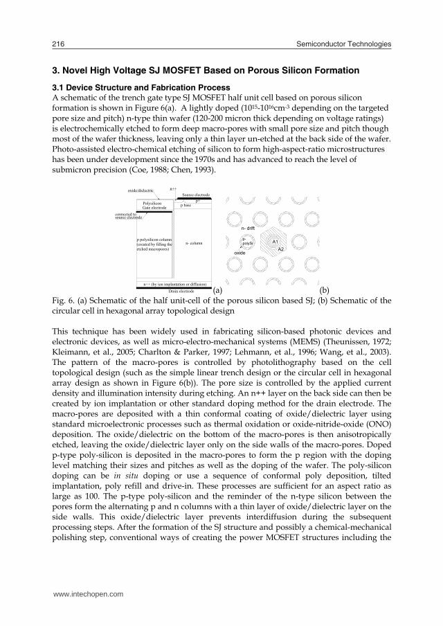
3.1 Device Structure and Fabrication Process A schematic of the trench gate type SJ MOSFET half unit cell based on porous silicon formation is shown in Figure 6(a). A lightly doped (1015-1016cm-3 depending on the targeted pore size and pitch) n-type thin wafer (120-200 micron thick depending on voltage ratings) is electrochemically etched to form deep macro-pores with small pore size and pitch though most of the wafer thickness, leaving only a thin layer un-etched at the back side of the wafer. Photo-assisted electro-chemical etching of silicon to form high-aspect-ratio microstructures has been under development since the 1970s and has advanced to reach the level of submicron precision (Coe, 1988; Chen, 1993).
n++ (by ion implantation or diffusion)
n- column
Drain electrode
p baseGate electrode
oxide/dielectric n++Source electrode
p+Polysilicon
source electrodeconnected to
p polysilicon column (created by filling the etched macropores)
(a)
A1A2
n- drift
p- polySi
oxide
(b) Fig. 6. (a) Schematic of the half unit-cell of the porous silicon based SJ; (b) Schematic of the circular cell in hexagonal array topological design This technique has been widely used in fabricating silicon-based photonic devices and electronic devices, as well as micro-electro-mechanical systems (MEMS) (Theunissen, 1972; Kleimann, et al., 2005; Charlton & Parker, 1997; Lehmann, et al., 1996; Wang, et al., 2003). The pattern of the macro-pores is controlled by photolithography based on the cell topological design (such as the simple linear trench design or the circular cell in hexagonal array design as shown in Figure 6(b)). The pore size is controlled by the applied current density and illumination intensity during etching. An n++ layer on the back side can then be created by ion implantation or other standard doping method for the drain electrode. The macro-pores are deposited with a thin conformal coating of oxide/dielectric layer using standard microelectronic processes such as thermal oxidation or oxide-nitride-oxide (ONO) deposition. The oxide/dielectric on the bottom of the macro-pores is then anisotropically etched, leaving the oxide/dielectric layer only on the side walls of the macro-pores. Doped p-type poly-silicon is deposited in the macro-pores to form the p region with the doping level matching their sizes and pitches as well as the doping of the wafer. The poly-silicon doping can be in situ doping or use a sequence of conformal poly deposition, tilted implantation, poly refill and drive-in. These processes are sufficient for an aspect ratio as large as 100. The p-type poly-silicon and the reminder of the n-type silicon between the pores form the alternating p and n columns with a thin layer of oxide/dielectric layer on the side walls. This oxide/dielectric layer prevents interdiffusion during the subsequent processing steps. After the formation of the SJ structure and possibly a chemical-mechanical polishing step, conventional ways of creating the power MOSFET structures including the
gate and source electrodes can be employed. This process can fabricate SJ structures with a column size of a couple of microns and depth up to a couple of hundred microns, with the potential to create SJ devices at voltages above 2000V.
3.2 Device Simulation Description We have used physically-based device simulation software Synopsys Sentaurus Device to perform the simulations. Fermi-Dirac statistics is employed in the carrier density calculation. For low field bulk mobility, Klaassen’s unified mobility model (Klaassen, 1992; Klaassen, 1992) is used, which considers the effects of lattice scattering, impurity scattering, carrier-carrier scattering, and impurity clustering effects at high concentration. The mobility degradation within the inversion layers is considered by employing Lombardi’s model (Lombardi, et al., 1988) that accounts for the effects of surface acoustic phonon scattering and surface roughness scattering. Canali’s model (Canali, et al., 1975) is used to account for the carrier velocity saturation in high electric fields. Doping-dependent Shockley-Read-Hall recombination and Auger recombination are considered. The breakdown of the device is simulated by employing Lackner’s avalanche generation model (Lackner, 1991). The device under consideration has a cell structure as shown in Figure 6(a) and uses the topological design of a circular cell in a hexagonal array (Figure 6(b)). In order to satisfy the charge compensation requirement, the size of the poly-silicon p columns and pitch of the p columns are designed by
21 AnAp , (1) where p is the doping density in the p-type poly-silicon column and n is the wafer doping density; A1 and A2 are the areas of the p-type poly-silicon and area of n-type silicon surrounding the p-poly, respectively, as shown in Figure 6(b). The depths of the p and n columns are taken as 160m; p-base depth is 2.7m and n+ source depth of 0.8m, giving a channel length of 1.9m. The gate oxide thickness is 50nm. Gaussian profiles are assumed for p-base and n+ source with the peak concentrations of 31017cm-3 and 1019cm-3, respectively. The thickness of the n-layer underneath the p and n columns is 5µm, and the n+ drain doping is 1019cm-3. In the baseline half unit-cell, the width of the p-poly-silicon is 1m, which is equivalent to a p-column diameter of 2m. The thickness of the oxide layer (between the p and n columns) and n-column width are 0.1m and 0.692m, respectively. This makes the p-column center-to-center distance to be 3.6m. The area ratio between the poly-silicon p-column and the n-type silicon surround it, A1/A2, is then ½. The doping level of the wafer is 91015cm-3 and the doping level of the p-poly-silicon column is 1.81016cm-3. In order to account for the cell topology of a circular cell in a hexagonal array, cylindrical symmetry is assumed in the two-dimensional device simulations for the half unit cell.
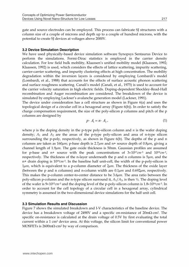
3.3 Simulation Results and Discussion Figure 7 shows the simulated breakdown and I-V characteristics of the baseline device. The device has a breakdown voltage of 2490V and a specific on-resistance of 20m·cm2. The specific on-resistance is calculated at the drain voltage of 0.5V by first evaluating the total current within a 1 cm2 device area. At this voltage, the silicon limit for conventional power MOSFETs is 2600m·cm2 by way of comparison.
www.intechopen.com
Concepts of Optimizing Power Semiconductor Devices Using Novel Nano-Structure for Low Losses 217
3. Novel High Voltage SJ MOSFET Based on Porous Silicon Formation
3.1 Device Structure and Fabrication Process A schematic of the trench gate type SJ MOSFET half unit cell based on porous silicon formation is shown in Figure 6(a). A lightly doped (1015-1016cm-3 depending on the targeted pore size and pitch) n-type thin wafer (120-200 micron thick depending on voltage ratings) is electrochemically etched to form deep macro-pores with small pore size and pitch though most of the wafer thickness, leaving only a thin layer un-etched at the back side of the wafer. Photo-assisted electro-chemical etching of silicon to form high-aspect-ratio microstructures has been under development since the 1970s and has advanced to reach the level of submicron precision (Coe, 1988; Chen, 1993).
n++ (by ion implantation or diffusion)
n- column
Drain electrode
p baseGate electrode
oxide/dielectric n++Source electrode
p+Polysilicon
source electrodeconnected to
p polysilicon column (created by filling the etched macropores)
(a)
A1A2
n- drift
p- polySi
oxide
(b) Fig. 6. (a) Schematic of the half unit-cell of the porous silicon based SJ; (b) Schematic of the circular cell in hexagonal array topological design This technique has been widely used in fabricating silicon-based photonic devices and electronic devices, as well as micro-electro-mechanical systems (MEMS) (Theunissen, 1972; Kleimann, et al., 2005; Charlton & Parker, 1997; Lehmann, et al., 1996; Wang, et al., 2003). The pattern of the macro-pores is controlled by photolithography based on the cell topological design (such as the simple linear trench design or the circular cell in hexagonal array design as shown in Figure 6(b)). The pore size is controlled by the applied current density and illumination intensity during etching. An n++ layer on the back side can then be created by ion implantation or other standard doping method for the drain electrode. The macro-pores are deposited with a thin conformal coating of oxide/dielectric layer using standard microelectronic processes such as thermal oxidation or oxide-nitride-oxide (ONO) deposition. The oxide/dielectric on the bottom of the macro-pores is then anisotropically etched, leaving the oxide/dielectric layer only on the side walls of the macro-pores. Doped p-type poly-silicon is deposited in the macro-pores to form the p region with the doping level matching their sizes and pitches as well as the doping of the wafer. The poly-silicon doping can be in situ doping or use a sequence of conformal poly deposition, tilted implantation, poly refill and drive-in. These processes are sufficient for an aspect ratio as large as 100. The p-type poly-silicon and the reminder of the n-type silicon between the pores form the alternating p and n columns with a thin layer of oxide/dielectric layer on the side walls. This oxide/dielectric layer prevents interdiffusion during the subsequent processing steps. After the formation of the SJ structure and possibly a chemical-mechanical polishing step, conventional ways of creating the power MOSFET structures including the
gate and source electrodes can be employed. This process can fabricate SJ structures with a column size of a couple of microns and depth up to a couple of hundred microns, with the potential to create SJ devices at voltages above 2000V.
3.2 Device Simulation Description We have used physically-based device simulation software Synopsys Sentaurus Device to perform the simulations. Fermi-Dirac statistics is employed in the carrier density calculation. For low field bulk mobility, Klaassen’s unified mobility model (Klaassen, 1992; Klaassen, 1992) is used, which considers the effects of lattice scattering, impurity scattering, carrier-carrier scattering, and impurity clustering effects at high concentration. The mobility degradation within the inversion layers is considered by employing Lombardi’s model (Lombardi, et al., 1988) that accounts for the effects of surface acoustic phonon scattering and surface roughness scattering. Canali’s model (Canali, et al., 1975) is used to account for the carrier velocity saturation in high electric fields. Doping-dependent Shockley-Read-Hall recombination and Auger recombination are considered. The breakdown of the device is simulated by employing Lackner’s avalanche generation model (Lackner, 1991). The device under consideration has a cell structure as shown in Figure 6(a) and uses the topological design of a circular cell in a hexagonal array (Figure 6(b)). In order to satisfy the charge compensation requirement, the size of the poly-silicon p columns and pitch of the p columns are designed by
21 AnAp , (1) where p is the doping density in the p-type poly-silicon column and n is the wafer doping density; A1 and A2 are the areas of the p-type poly-silicon and area of n-type silicon surrounding the p-poly, respectively, as shown in Figure 6(b). The depths of the p and n columns are taken as 160m; p-base depth is 2.7m and n+ source depth of 0.8m, giving a channel length of 1.9m. The gate oxide thickness is 50nm. Gaussian profiles are assumed for p-base and n+ source with the peak concentrations of 31017cm-3 and 1019cm-3, respectively. The thickness of the n-layer underneath the p and n columns is 5µm, and the n+ drain doping is 1019cm-3. In the baseline half unit-cell, the width of the p-poly-silicon is 1m, which is equivalent to a p-column diameter of 2m. The thickness of the oxide layer (between the p and n columns) and n-column width are 0.1m and 0.692m, respectively. This makes the p-column center-to-center distance to be 3.6m. The area ratio between the poly-silicon p-column and the n-type silicon surround it, A1/A2, is then ½. The doping level of the wafer is 91015cm-3 and the doping level of the p-poly-silicon column is 1.81016cm-3. In order to account for the cell topology of a circular cell in a hexagonal array, cylindrical symmetry is assumed in the two-dimensional device simulations for the half unit cell.
3.3 Simulation Results and Discussion Figure 7 shows the simulated breakdown and I-V characteristics of the baseline device. The device has a breakdown voltage of 2490V and a specific on-resistance of 20m·cm2. The specific on-resistance is calculated at the drain voltage of 0.5V by first evaluating the total current within a 1 cm2 device area. At this voltage, the silicon limit for conventional power MOSFETs is 2600m·cm2 by way of comparison.
www.intechopen.com
Semiconductor Technologies218
Drain Voltage (V)
Dra
inC
urre
nt(A
)
0 500 1000 1500 2000 2500
10-13
10-12
10-11
10-10
(a) Drain Voltage (V)
Dra
inC
urre
nt(A
/cel
l)
0 1 2 3 4 50
5E-06
1E-05
1.5E-05
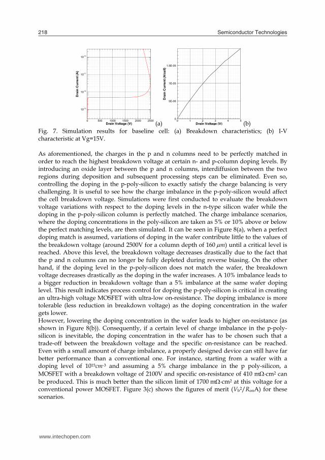
(b) Fig. 7. Simulation results for baseline cell: (a) Breakdown characteristics; (b) I-V characteristic at Vg=15V. As aforementioned, the charges in the p and n columns need to be perfectly matched in order to reach the highest breakdown voltage at certain n- and p-column doping levels. By introducing an oxide layer between the p and n columns, interdiffusion between the two regions during deposition and subsequent processing steps can be eliminated. Even so, controlling the doping in the p-poly-silicon to exactly satisfy the charge balancing is very challenging. It is useful to see how the charge imbalance in the p-poly-silicon would affect the cell breakdown voltage. Simulations were first conducted to evaluate the breakdown voltage variations with respect to the doping levels in the n-type silicon wafer while the doping in the p-poly-silicon column is perfectly matched. The charge imbalance scenarios, where the doping concentrations in the poly-silicon are taken as 5% or 10% above or below the perfect matching levels, are then simulated. It can be seen in Figure 8(a), when a perfect doping match is assumed, variations of doping in the wafer contribute little to the values of the breakdown voltage (around 2500V for a column depth of 160m) until a critical level is reached. Above this level, the breakdown voltage decreases drastically due to the fact that the p and n columns can no longer be fully depleted during reverse biasing. On the other hand, if the doping level in the p-poly-silicon does not match the wafer, the breakdown voltage decreases drastically as the doping in the wafer increases. A 10% imbalance leads to a bigger reduction in breakdown voltage than a 5% imbalance at the same wafer doping level. This result indicates process control for doping the p-poly-silicon is critical in creating an ultra-high voltage MOSFET with ultra-low on-resistance. The doping imbalance is more tolerable (less reduction in breakdown voltage) as the doping concentration in the wafer gets lower. However, lowering the doping concentration in the wafer leads to higher on-resistance (as shown in Figure 8(b)). Consequently, if a certain level of charge imbalance in the p-poly-silicon is inevitable, the doping concentration in the wafer has to be chosen such that a trade-off between the breakdown voltage and the specific on-resistance can be reached. Even with a small amount of charge imbalance, a properly designed device can still have far better performance than a conventional one. For instance, starting from a wafer with a doping level of 1015cm-3 and assuming a 5% charge imbalance in the p poly-silicon, a MOSFET with a breakdown voltage of 2100V and specific on-resistance of 410 m·cm2 can be produced. This is much better than the silicon limit of 1700 m·cm2 at this voltage for a conventional power MOSFET. Figure 3(c) shows the figures of merit (Vb2/RonA) for these scenarios.
Doping in n silicon wafer (cm-3)1e+15 1e+16
Brea
kdow
n Vo
ltage
(V)
0
500
1000
1500
2000
2500
Perfect match90% match95% match105% match110% match
(a) Doping in n silicon wafer (cm-3)0 5e+15 1e+16 2e+16 2e+16
Spe
cific
On-
resi
stan
ce (O
hm/c
m2 )
0.1
0.2
0.3
0.4
0.5
Perfect match90% match95% match105% match110% match
(b)
Doping in n silicon wafer (cm-3)1e+15 1e+16
Figu
re o
f Mer
it (M
W/c
m2 )
1
10
100
1000
Perfect match90% match95% match105% match110% match
(c) Fig.3. (8) Breakdown voltage, (b) specific on-resistance, and (c) figure of merit vs. doping concentration of silicon wafer for various charge imbalance conditions It shows that a figure of merit of more than 500 MW/cm2 is possible if perfect control of the p-poly-doping can be achieved. A small amount of charge imbalance greatly reduces the figure of merit. However, with a 5% charge imbalance, figures of merit between 10 and 30 MW/cm2 are achievable for wafer doping levels between 1015 to 1016 cm-3, which covers breakdown voltages between 2100 and 1000 V. This is still much better than the figures of merit of silicon limits for conventional power MOSFETs, which are between 2.5 and 4 MW/cm2 at these voltage ratings.
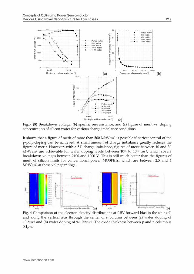
(a) (b) Fig. 4 Comparison of the electron density distributions at 0.5V forward bias in the unit cell and along the vertical axis through the center of n column between (a) wafer doping of 1015cm-3 and (b) wafer doping of 91015cm-3. The oxide thickness between p and n column is 0.1m.
www.intechopen.com
Concepts of Optimizing Power Semiconductor Devices Using Novel Nano-Structure for Low Losses 219
Drain Voltage (V)
Dra
inC
urre
nt(A
)
0 500 1000 1500 2000 2500
10-13
10-12
10-11
10-10
(a) Drain Voltage (V)
Dra
inC
urre
nt(A
/cel
l)
0 1 2 3 4 50
5E-06
1E-05
1.5E-05
(b) Fig. 7. Simulation results for baseline cell: (a) Breakdown characteristics; (b) I-V characteristic at Vg=15V. As aforementioned, the charges in the p and n columns need to be perfectly matched in order to reach the highest breakdown voltage at certain n- and p-column doping levels. By introducing an oxide layer between the p and n columns, interdiffusion between the two regions during deposition and subsequent processing steps can be eliminated. Even so, controlling the doping in the p-poly-silicon to exactly satisfy the charge balancing is very challenging. It is useful to see how the charge imbalance in the p-poly-silicon would affect the cell breakdown voltage. Simulations were first conducted to evaluate the breakdown voltage variations with respect to the doping levels in the n-type silicon wafer while the doping in the p-poly-silicon column is perfectly matched. The charge imbalance scenarios, where the doping concentrations in the poly-silicon are taken as 5% or 10% above or below the perfect matching levels, are then simulated. It can be seen in Figure 8(a), when a perfect doping match is assumed, variations of doping in the wafer contribute little to the values of the breakdown voltage (around 2500V for a column depth of 160m) until a critical level is reached. Above this level, the breakdown voltage decreases drastically due to the fact that the p and n columns can no longer be fully depleted during reverse biasing. On the other hand, if the doping level in the p-poly-silicon does not match the wafer, the breakdown voltage decreases drastically as the doping in the wafer increases. A 10% imbalance leads to a bigger reduction in breakdown voltage than a 5% imbalance at the same wafer doping level. This result indicates process control for doping the p-poly-silicon is critical in creating an ultra-high voltage MOSFET with ultra-low on-resistance. The doping imbalance is more tolerable (less reduction in breakdown voltage) as the doping concentration in the wafer gets lower. However, lowering the doping concentration in the wafer leads to higher on-resistance (as shown in Figure 8(b)). Consequently, if a certain level of charge imbalance in the p-poly-silicon is inevitable, the doping concentration in the wafer has to be chosen such that a trade-off between the breakdown voltage and the specific on-resistance can be reached. Even with a small amount of charge imbalance, a properly designed device can still have far better performance than a conventional one. For instance, starting from a wafer with a doping level of 1015cm-3 and assuming a 5% charge imbalance in the p poly-silicon, a MOSFET with a breakdown voltage of 2100V and specific on-resistance of 410 m·cm2 can be produced. This is much better than the silicon limit of 1700 m·cm2 at this voltage for a conventional power MOSFET. Figure 3(c) shows the figures of merit (Vb2/RonA) for these scenarios.
Doping in n silicon wafer (cm-3)1e+15 1e+16
Brea
kdow
n Vo
ltage
(V)
0
500
1000
1500
2000
2500
Perfect match90% match95% match105% match110% match
(a) Doping in n silicon wafer (cm-3)0 5e+15 1e+16 2e+16 2e+16
Spe
cific
On-
resi
stan
ce (O
hm/c
m2 )
0.1
0.2
0.3
0.4
0.5
Perfect match90% match95% match105% match110% match
(b)
Doping in n silicon wafer (cm-3)1e+15 1e+16
Figu
re o
f Mer
it (M
W/c
m2 )
1
10
100
1000
Perfect match90% match95% match105% match110% match
(c) Fig.3. (8) Breakdown voltage, (b) specific on-resistance, and (c) figure of merit vs. doping concentration of silicon wafer for various charge imbalance conditions It shows that a figure of merit of more than 500 MW/cm2 is possible if perfect control of the p-poly-doping can be achieved. A small amount of charge imbalance greatly reduces the figure of merit. However, with a 5% charge imbalance, figures of merit between 10 and 30 MW/cm2 are achievable for wafer doping levels between 1015 to 1016 cm-3, which covers breakdown voltages between 2100 and 1000 V. This is still much better than the figures of merit of silicon limits for conventional power MOSFETs, which are between 2.5 and 4 MW/cm2 at these voltage ratings.
(a) (b) Fig. 4 Comparison of the electron density distributions at 0.5V forward bias in the unit cell and along the vertical axis through the center of n column between (a) wafer doping of 1015cm-3 and (b) wafer doping of 91015cm-3. The oxide thickness between p and n column is 0.1m.
www.intechopen.com
Semiconductor Technologies220
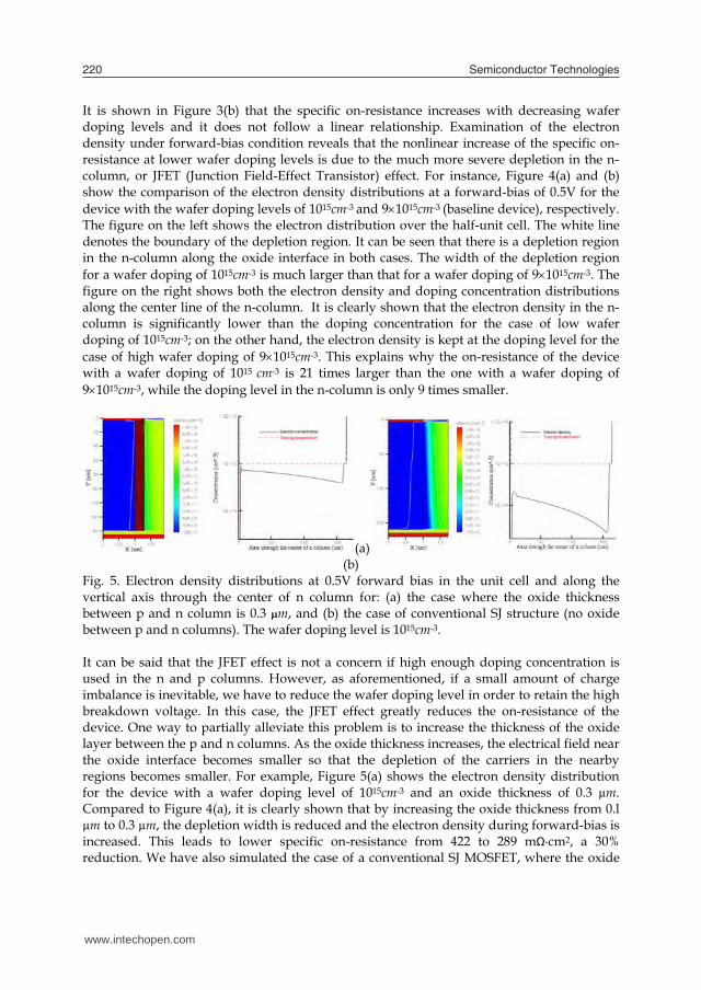
It is shown in Figure 3(b) that the specific on-resistance increases with decreasing wafer doping levels and it does not follow a linear relationship. Examination of the electron density under forward-bias condition reveals that the nonlinear increase of the specific on-resistance at lower wafer doping levels is due to the much more severe depletion in the n-column, or JFET (Junction Field-Effect Transistor) effect. For instance, Figure 4(a) and (b) show the comparison of the electron density distributions at a forward-bias of 0.5V for the device with the wafer doping levels of 1015cm-3 and 91015cm-3 (baseline device), respectively. The figure on the left shows the electron distribution over the half-unit cell. The white line denotes the boundary of the depletion region. It can be seen that there is a depletion region in the n-column along the oxide interface in both cases. The width of the depletion region for a wafer doping of 1015cm-3 is much larger than that for a wafer doping of 91015cm-3. The figure on the right shows both the electron density and doping concentration distributions along the center line of the n-column. It is clearly shown that the electron density in the n-column is significantly lower than the doping concentration for the case of low wafer doping of 1015cm-3; on the other hand, the electron density is kept at the doping level for the case of high wafer doping of 91015cm-3. This explains why the on-resistance of the device with a wafer doping of 1015 cm-3 is 21 times larger than the one with a wafer doping of 91015cm-3, while the doping level in the n-column is only 9 times smaller.
(a) (b)
Fig. 5. Electron density distributions at 0.5V forward bias in the unit cell and along the vertical axis through the center of n column for: (a) the case where the oxide thickness between p and n column is 0.3 µm, and (b) the case of conventional SJ structure (no oxide between p and n columns). The wafer doping level is 1015cm-3. It can be said that the JFET effect is not a concern if high enough doping concentration is used in the n and p columns. However, as aforementioned, if a small amount of charge imbalance is inevitable, we have to reduce the wafer doping level in order to retain the high breakdown voltage. In this case, the JFET effect greatly reduces the on-resistance of the device. One way to partially alleviate this problem is to increase the thickness of the oxide layer between the p and n columns. As the oxide thickness increases, the electrical field near the oxide interface becomes smaller so that the depletion of the carriers in the nearby regions becomes smaller. For example, Figure 5(a) shows the electron density distribution for the device with a wafer doping level of 1015cm-3 and an oxide thickness of 0.3 µm. Compared to Figure 4(a), it is clearly shown that by increasing the oxide thickness from 0.l µm to 0.3 µm, the depletion width is reduced and the electron density during forward-bias is increased. This leads to lower specific on-resistance from 422 to 289 mΩ·cm2, a 30% reduction. We have also simulated the case of a conventional SJ MOSFET, where the oxide
layer is nonexistent. It turns out that, at the same wafer doping level of 1015cm-3, the JFET effect is much more severe as shown in Figure 5(b); the specific on-resistance turns out to be 1084 mΩ·cm2, almost 4 times that of the device with a 0.3 µm oxide layer. Further simulations on device breakdown have shown that adding an oxide layer between the p and n columns has almost no effect on the breakdown voltage. This clearly shows that putting an oxide layer between the p and n columns not only helps to prevent interdiffusion between the columns during processing but increases the performance of the device as well by reducing the JFET effect at lower wafer doping levels. This is important when charge imbalance is expected and wafer doping is purposely reduced to maintain the device breakdown voltage.
Oxide thickness (m)0.0 0.1 0.2 0.3 0.4
Spe
cific
on-
resi
stan
ce (
cm2 )
0.01
0.1
1
10
100
5e14 1e15 2e15 3e15 4e15 6e15 9e15
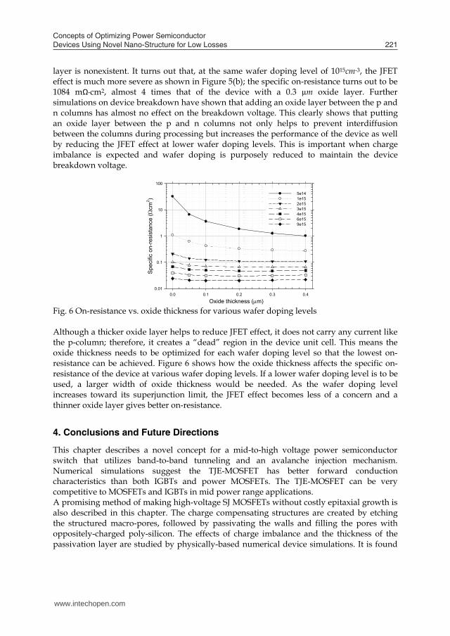
Fig. 6 On-resistance vs. oxide thickness for various wafer doping levels Although a thicker oxide layer helps to reduce JFET effect, it does not carry any current like the p-column; therefore, it creates a “dead” region in the device unit cell. This means the oxide thickness needs to be optimized for each wafer doping level so that the lowest on-resistance can be achieved. Figure 6 shows how the oxide thickness affects the specific on-resistance of the device at various wafer doping levels. If a lower wafer doping level is to be used, a larger width of oxide thickness would be needed. As the wafer doping level increases toward its superjunction limit, the JFET effect becomes less of a concern and a thinner oxide layer gives better on-resistance.
4. Conclusions and Future Directions
This chapter describes a novel concept for a mid-to-high voltage power semiconductor switch that utilizes band-to-band tunneling and an avalanche injection mechanism. Numerical simulations suggest the TJE-MOSFET has better forward conduction characteristics than both IGBTs and power MOSFETs. The TJE-MOSFET can be very competitive to MOSFETs and IGBTs in mid power range applications. A promising method of making high-voltage SJ MOSFETs without costly epitaxial growth is also described in this chapter. The charge compensating structures are created by etching the structured macro-pores, followed by passivating the walls and filling the pores with oppositely-charged poly-silicon. The effects of charge imbalance and the thickness of the passivation layer are studied by physically-based numerical device simulations. It is found
www.intechopen.com
Concepts of Optimizing Power Semiconductor Devices Using Novel Nano-Structure for Low Losses 221
It is shown in Figure 3(b) that the specific on-resistance increases with decreasing wafer doping levels and it does not follow a linear relationship. Examination of the electron density under forward-bias condition reveals that the nonlinear increase of the specific on-resistance at lower wafer doping levels is due to the much more severe depletion in the n-column, or JFET (Junction Field-Effect Transistor) effect. For instance, Figure 4(a) and (b) show the comparison of the electron density distributions at a forward-bias of 0.5V for the device with the wafer doping levels of 1015cm-3 and 91015cm-3 (baseline device), respectively. The figure on the left shows the electron distribution over the half-unit cell. The white line denotes the boundary of the depletion region. It can be seen that there is a depletion region in the n-column along the oxide interface in both cases. The width of the depletion region for a wafer doping of 1015cm-3 is much larger than that for a wafer doping of 91015cm-3. The figure on the right shows both the electron density and doping concentration distributions along the center line of the n-column. It is clearly shown that the electron density in the n-column is significantly lower than the doping concentration for the case of low wafer doping of 1015cm-3; on the other hand, the electron density is kept at the doping level for the case of high wafer doping of 91015cm-3. This explains why the on-resistance of the device with a wafer doping of 1015 cm-3 is 21 times larger than the one with a wafer doping of 91015cm-3, while the doping level in the n-column is only 9 times smaller.
(a) (b)
Fig. 5. Electron density distributions at 0.5V forward bias in the unit cell and along the vertical axis through the center of n column for: (a) the case where the oxide thickness between p and n column is 0.3 µm, and (b) the case of conventional SJ structure (no oxide between p and n columns). The wafer doping level is 1015cm-3. It can be said that the JFET effect is not a concern if high enough doping concentration is used in the n and p columns. However, as aforementioned, if a small amount of charge imbalance is inevitable, we have to reduce the wafer doping level in order to retain the high breakdown voltage. In this case, the JFET effect greatly reduces the on-resistance of the device. One way to partially alleviate this problem is to increase the thickness of the oxide layer between the p and n columns. As the oxide thickness increases, the electrical field near the oxide interface becomes smaller so that the depletion of the carriers in the nearby regions becomes smaller. For example, Figure 5(a) shows the electron density distribution for the device with a wafer doping level of 1015cm-3 and an oxide thickness of 0.3 µm. Compared to Figure 4(a), it is clearly shown that by increasing the oxide thickness from 0.l µm to 0.3 µm, the depletion width is reduced and the electron density during forward-bias is increased. This leads to lower specific on-resistance from 422 to 289 mΩ·cm2, a 30% reduction. We have also simulated the case of a conventional SJ MOSFET, where the oxide
layer is nonexistent. It turns out that, at the same wafer doping level of 1015cm-3, the JFET effect is much more severe as shown in Figure 5(b); the specific on-resistance turns out to be 1084 mΩ·cm2, almost 4 times that of the device with a 0.3 µm oxide layer. Further simulations on device breakdown have shown that adding an oxide layer between the p and n columns has almost no effect on the breakdown voltage. This clearly shows that putting an oxide layer between the p and n columns not only helps to prevent interdiffusion between the columns during processing but increases the performance of the device as well by reducing the JFET effect at lower wafer doping levels. This is important when charge imbalance is expected and wafer doping is purposely reduced to maintain the device breakdown voltage.
Oxide thickness (m)0.0 0.1 0.2 0.3 0.4
Spe
cific
on-
resi
stan
ce (
cm2 )
0.01
0.1
1
10
100
5e14 1e15 2e15 3e15 4e15 6e15 9e15
Fig. 6 On-resistance vs. oxide thickness for various wafer doping levels Although a thicker oxide layer helps to reduce JFET effect, it does not carry any current like the p-column; therefore, it creates a “dead” region in the device unit cell. This means the oxide thickness needs to be optimized for each wafer doping level so that the lowest on-resistance can be achieved. Figure 6 shows how the oxide thickness affects the specific on-resistance of the device at various wafer doping levels. If a lower wafer doping level is to be used, a larger width of oxide thickness would be needed. As the wafer doping level increases toward its superjunction limit, the JFET effect becomes less of a concern and a thinner oxide layer gives better on-resistance.
4. Conclusions and Future Directions
This chapter describes a novel concept for a mid-to-high voltage power semiconductor switch that utilizes band-to-band tunneling and an avalanche injection mechanism. Numerical simulations suggest the TJE-MOSFET has better forward conduction characteristics than both IGBTs and power MOSFETs. The TJE-MOSFET can be very competitive to MOSFETs and IGBTs in mid power range applications. A promising method of making high-voltage SJ MOSFETs without costly epitaxial growth is also described in this chapter. The charge compensating structures are created by etching the structured macro-pores, followed by passivating the walls and filling the pores with oppositely-charged poly-silicon. The effects of charge imbalance and the thickness of the passivation layer are studied by physically-based numerical device simulations. It is found
www.intechopen.com
Semiconductor Technologies222
that even with a small amount of charge imbalance, the proposed method can still produce high-voltage MOSFETs with much better performance than existing technology. A thick oxide layer between the p and n columns is found to be helpful of alleviating the JFET effects when the doping concentrations in the p and n columns are low. In comparison with a conventional superjunction structure, the inclusion of an oxide layer between p and n columns is found to help increase the device efficiency in addition to its ability to prevent dopant interdiffusion.
5. References
Aydin, C., Zaslavsky, A., Luryi, S., Cristoloveanu, S., Mariolle, D., Fraboulet, D., and Deleonibus, S. (2004). Lateral interband tunneling transistor in silicon-on-insulator. Applied Physics Letters. vol. 84, no. 10, pp. 1780-1782.
Canali, C., Majni, G., Minder, R., and Ottaviani, G. (1975). Electron and Hole Drift Velocity Measurements in Silicon and Their Empirical Relation to Electric Field and Temperature. IEEE Transactions on Electron Devices. vol. 22, no. 11, pp. 1045-1047.
Charlton, M.D.B. and Parker, G.J. (1997). Fabrication of High Aspect Ratio Silicon Microstructures by Anodic Etching. Journal of Micromechanics and Microengineering. vol. 7, pp.155-158.
Chen, X. (1993)Semiconductor power devices with alternating conductivity type high-voltage breakdown regions. US Patent 5216275.
Chen, Y., and Liang, Y. C. (2007). Design of Gradient Oxide-Bypassed Superjunction Power MOSFETE Devices. IEEE Transactions on Power Electronics, vol. 22, no. 4, pp. 1303-1310.
Coe, D. J. (1998). High voltage semiconductor device. US Patent 4754310. Deboy, G., März, M., Stengle, J.-P., Strack, H., Tihanyi, J., and Weber, H. (1998). A new
generation of high voltage MOSFETs breaks the limit line of silicon. Technical Digest of IEDM 98, Dec. 1998, pp. 683-685.
Fujihira, T. (1997). Theory of Semiconductor Superjunction Devices. Japan Journal of Applied Physcis, vol. 36, no.10, pp. 6254-6262.
Gan, K. P., Liang, Y. C., Samudra, G. S., and Yong, L. (2001). A Simple Technology for Superjunction Device Fabrication: Polyflanked VDMOSFET. IEEE Electron Device Letters, vol. 22, no. 8, pp. 407-409.
Hu, C. (1979). Optimum doping profile for minimum ohmic resistance and high-breakdown voltage. IEEE Transactions on Electron Devices, vol. 26, no. 3, pp. 243-244.
Klaassen, D. B. M. (1992). A unified mobility model for device simulation--I. Model equations and concentration dependence. Solid-State Electron. vol. 35, no. 7, pp. 953-959.
Klaassen, D. B. M. (1992). A unified mobility model for device simulation--II. Temperature dependence of carrier mobility and lifetime. Solid-State Electron. vol. 35, no. 7, pp. 961-967.
Kleimann, P., Badel, X., and Linnros, J. (2005). Toward the Formation of Three-Dimensional Nanostructures by Electrochemical Etching of Silicon. Applied Physics Letters. vol. 86, pp.183108.
Lackner, T. (1991). Avalanche Multiplication in Semiconductors: A Modification of Chynoweth's Law. Solid-State Electron. vol. 34, no. 1, pp. 33-42.
Lehmann, V., Honlein, W., Reisinger, H., Spitzer, A., Wendt, H., and Willer, J. (1996). A Novel Capacitor Technology Based on Porous Silicon. Thin Solid Films. vol.276, pp.138-142.
Liang, Y. C., Gan, K. P., and Samudra, G. S. (2001). Oxide-bypassed VDMOS (OBVDMOS): An alternative to superjunction high voltage MOS power devices. IEEE Electron Device Letters. vol. 22, no. 8, pp. 407-409.
Lombardi, C., Manzini, S., Saporito, A., and Vanzi, M. (1988). A physically based mobility model for numerical simulation of nonplanar devices. Computer-Aided Design of Integrated Circuits and Systems, IEEE Transactions on. vol. 7, no. 11, pp. 1164-1171.
Minato, T., Nitta, T., Uenisi, A., Yano, M., Harada, M., and Hine, S. (2000). Which is cooler, Trench or Multi-Epitaxy. in Proc.of the 12th International Symposium on Power Semiconductor Devices and ICs, Toulous, France: pp. 73-76, 2000.
Miura, Y., Ninomiya, H., and Kobayashi, K. (2005). High Performance Superjunction UMOSFETs with Split P-Colums Fabricated by Multi-Ion-Implantations. in Proc.of the 17th International Symposium on Power Semiconductor Devices & IC's, Santa Barbara, CA: pp. 1-4.
Onishi, Y., Iwamoto, S., Sato, T., Nagaoka, T., Ueno, K., and Fujihira, T. (2002). 24 mcm2 680 V silicon superjunction MOSFET. in Proc.of the 14th International Symposium on Power Semiconductor Devices and ICs, pp. 241-244.
Rochefort, C., van Dalen, R., Duhayon, N., and Vandervorst, W. (2002). Manufacturing of high aspect-ratio p-n junctions using vapor phase doping for application in multi-Resurf devices. in Proc.of the 14th International Symposium on Power Semiconductor Devices and ICs, pp. 237-240, 2002.
Rub, M., Bar, M., Deboy, G., Niedernostheide, F. J., Schmitt, M., Schulze, H. J., and Willmeroth, A. (2004). 550V Superjunction 3.9mm2 Transistor Formed by 25 MeV Masked Boron Implantation. in Proc.of the 16th International Symposium on Power Semiconductor Devices & IC's, Kitakyushu, Japan: pp. 445-458.
Shenoy, P.M., Bhalla, A., and Dolny, G.M. (1999). Analysis of the Effect of Charge Imbalance on the Static and Dynamic Characteristics of the Super Junction MOSFET. Proceedings of ISPSD’99, May 1999, pp. 99-102.
Solomon, P. M., Frank, D. J., D'Emic, C., Dokumaci, O., Ronsheim, P., and Haensch, W. E., Universal tunneling behavior in technologically relevant P/N junction diodes. Journal of Applied Physics. vol. 95, no. 10, pp. 5800-5812.
Theunissen, M.J.J. (1972). Etch Channel Formation during Anodic Dissolution of N-Type Silicon in Aqueous Hydrofluoric Acid. Solid-State Science and Technology. vol.119, no. 3, pp.351-360.
von Borany, J., Friedrich, M., Rüb, M., Deboy, G., Butschke, J., and Letzkus, F. (2004). Application of Ultra-High Energy Boron Implantation for Superjunction Power (CoolMOS TM) Devices. Nuclear Inst. and Methods in Physics Research, B, vol. 237, no. 1-2, pp. 62-67.
W. Saito, I. Omura, S. Aida, S. Koduki, M. Izumisawa, H. Yoshioka, and T. Ogura, "Over 1000V Semi-Superjunction MOSFET with Ultra-Low On-Resistance Blow the Si-Limit," in Proc.of 17th International Symposium on Power Semiconductor Device & IC's, Santa Barbara, CA: 2005.
www.intechopen.com
Concepts of Optimizing Power Semiconductor Devices Using Novel Nano-Structure for Low Losses 223
that even with a small amount of charge imbalance, the proposed method can still produce high-voltage MOSFETs with much better performance than existing technology. A thick oxide layer between the p and n columns is found to be helpful of alleviating the JFET effects when the doping concentrations in the p and n columns are low. In comparison with a conventional superjunction structure, the inclusion of an oxide layer between p and n columns is found to help increase the device efficiency in addition to its ability to prevent dopant interdiffusion.
5. References
Aydin, C., Zaslavsky, A., Luryi, S., Cristoloveanu, S., Mariolle, D., Fraboulet, D., and Deleonibus, S. (2004). Lateral interband tunneling transistor in silicon-on-insulator. Applied Physics Letters. vol. 84, no. 10, pp. 1780-1782.
Canali, C., Majni, G., Minder, R., and Ottaviani, G. (1975). Electron and Hole Drift Velocity Measurements in Silicon and Their Empirical Relation to Electric Field and Temperature. IEEE Transactions on Electron Devices. vol. 22, no. 11, pp. 1045-1047.
Charlton, M.D.B. and Parker, G.J. (1997). Fabrication of High Aspect Ratio Silicon Microstructures by Anodic Etching. Journal of Micromechanics and Microengineering. vol. 7, pp.155-158.
Chen, X. (1993)Semiconductor power devices with alternating conductivity type high-voltage breakdown regions. US Patent 5216275.
Chen, Y., and Liang, Y. C. (2007). Design of Gradient Oxide-Bypassed Superjunction Power MOSFETE Devices. IEEE Transactions on Power Electronics, vol. 22, no. 4, pp. 1303-1310.
Coe, D. J. (1998). High voltage semiconductor device. US Patent 4754310. Deboy, G., März, M., Stengle, J.-P., Strack, H., Tihanyi, J., and Weber, H. (1998). A new
generation of high voltage MOSFETs breaks the limit line of silicon. Technical Digest of IEDM 98, Dec. 1998, pp. 683-685.
Fujihira, T. (1997). Theory of Semiconductor Superjunction Devices. Japan Journal of Applied Physcis, vol. 36, no.10, pp. 6254-6262.
Gan, K. P., Liang, Y. C., Samudra, G. S., and Yong, L. (2001). A Simple Technology for Superjunction Device Fabrication: Polyflanked VDMOSFET. IEEE Electron Device Letters, vol. 22, no. 8, pp. 407-409.
Hu, C. (1979). Optimum doping profile for minimum ohmic resistance and high-breakdown voltage. IEEE Transactions on Electron Devices, vol. 26, no. 3, pp. 243-244.
Klaassen, D. B. M. (1992). A unified mobility model for device simulation--I. Model equations and concentration dependence. Solid-State Electron. vol. 35, no. 7, pp. 953-959.
Klaassen, D. B. M. (1992). A unified mobility model for device simulation--II. Temperature dependence of carrier mobility and lifetime. Solid-State Electron. vol. 35, no. 7, pp. 961-967.
Kleimann, P., Badel, X., and Linnros, J. (2005). Toward the Formation of Three-Dimensional Nanostructures by Electrochemical Etching of Silicon. Applied Physics Letters. vol. 86, pp.183108.
Lackner, T. (1991). Avalanche Multiplication in Semiconductors: A Modification of Chynoweth's Law. Solid-State Electron. vol. 34, no. 1, pp. 33-42.
Lehmann, V., Honlein, W., Reisinger, H., Spitzer, A., Wendt, H., and Willer, J. (1996). A Novel Capacitor Technology Based on Porous Silicon. Thin Solid Films. vol.276, pp.138-142.
Liang, Y. C., Gan, K. P., and Samudra, G. S. (2001). Oxide-bypassed VDMOS (OBVDMOS): An alternative to superjunction high voltage MOS power devices. IEEE Electron Device Letters. vol. 22, no. 8, pp. 407-409.
Lombardi, C., Manzini, S., Saporito, A., and Vanzi, M. (1988). A physically based mobility model for numerical simulation of nonplanar devices. Computer-Aided Design of Integrated Circuits and Systems, IEEE Transactions on. vol. 7, no. 11, pp. 1164-1171.
Minato, T., Nitta, T., Uenisi, A., Yano, M., Harada, M., and Hine, S. (2000). Which is cooler, Trench or Multi-Epitaxy. in Proc.of the 12th International Symposium on Power Semiconductor Devices and ICs, Toulous, France: pp. 73-76, 2000.
Miura, Y., Ninomiya, H., and Kobayashi, K. (2005). High Performance Superjunction UMOSFETs with Split P-Colums Fabricated by Multi-Ion-Implantations. in Proc.of the 17th International Symposium on Power Semiconductor Devices & IC's, Santa Barbara, CA: pp. 1-4.
Onishi, Y., Iwamoto, S., Sato, T., Nagaoka, T., Ueno, K., and Fujihira, T. (2002). 24 mcm2 680 V silicon superjunction MOSFET. in Proc.of the 14th International Symposium on Power Semiconductor Devices and ICs, pp. 241-244.
Rochefort, C., van Dalen, R., Duhayon, N., and Vandervorst, W. (2002). Manufacturing of high aspect-ratio p-n junctions using vapor phase doping for application in multi-Resurf devices. in Proc.of the 14th International Symposium on Power Semiconductor Devices and ICs, pp. 237-240, 2002.
Rub, M., Bar, M., Deboy, G., Niedernostheide, F. J., Schmitt, M., Schulze, H. J., and Willmeroth, A. (2004). 550V Superjunction 3.9mm2 Transistor Formed by 25 MeV Masked Boron Implantation. in Proc.of the 16th International Symposium on Power Semiconductor Devices & IC's, Kitakyushu, Japan: pp. 445-458.
Shenoy, P.M., Bhalla, A., and Dolny, G.M. (1999). Analysis of the Effect of Charge Imbalance on the Static and Dynamic Characteristics of the Super Junction MOSFET. Proceedings of ISPSD’99, May 1999, pp. 99-102.
Solomon, P. M., Frank, D. J., D'Emic, C., Dokumaci, O., Ronsheim, P., and Haensch, W. E., Universal tunneling behavior in technologically relevant P/N junction diodes. Journal of Applied Physics. vol. 95, no. 10, pp. 5800-5812.
Theunissen, M.J.J. (1972). Etch Channel Formation during Anodic Dissolution of N-Type Silicon in Aqueous Hydrofluoric Acid. Solid-State Science and Technology. vol.119, no. 3, pp.351-360.
von Borany, J., Friedrich, M., Rüb, M., Deboy, G., Butschke, J., and Letzkus, F. (2004). Application of Ultra-High Energy Boron Implantation for Superjunction Power (CoolMOS TM) Devices. Nuclear Inst. and Methods in Physics Research, B, vol. 237, no. 1-2, pp. 62-67.
W. Saito, I. Omura, S. Aida, S. Koduki, M. Izumisawa, H. Yoshioka, and T. Ogura, "Over 1000V Semi-Superjunction MOSFET with Ultra-Low On-Resistance Blow the Si-Limit," in Proc.of 17th International Symposium on Power Semiconductor Device & IC's, Santa Barbara, CA: 2005.
www.intechopen.com
Semiconductor Technologies224
Wang, L., Nichelatti, A., Schellevis, H., de Boer, C., Visser, C., Nguyen, T.N., and Sarro, P.M. (2003). High Aspect Ratio Through-Wafer Interconnections for 3D-Microsystems. Proc. of IEEE MEMS-03 Kyoto, pp.634-637.
Ye, H. and Haldar, P., (2008). A MOS Gated Power Semiconductor Switch Using Band-to-Band Tunneling and Avalanche Injection Mechanism. IEEE Trans. On Electron Devices. Vol.55, No.6, pp.1524-1528.
Ye, H. and Haldar, P. (2008). Optimization of the Porous Silicon Based Superjunction Power MOSFET. IEEE Trans. On Electron Devices. Vol.55, No.8, pp.2246-2251.
www.intechopen.com
Semiconductor TechnologiesEdited by Jan Grym
ISBN 978-953-307-080-3Hard cover, 462 pagesPublisher InTechPublished online 01, April, 2010Published in print edition April, 2010
InTech EuropeUniversity Campus STeP Ri Slavka Krautzeka 83/A 51000 Rijeka, Croatia Phone: +385 (51) 770 447 Fax: +385 (51) 686 166www.intechopen.com
InTech ChinaUnit 405, Office Block, Hotel Equatorial Shanghai No.65, Yan An Road (West), Shanghai, 200040, China
Phone: +86-21-62489820 Fax: +86-21-62489821
Semiconductor technologies continue to evolve and amaze us. New materials, new structures, newmanufacturing tools, and new advancements in modelling and simulation form a breeding ground for novelhigh performance electronic and photonic devices. This book covers all aspects of semiconductor technologyconcerning materials, technological processes, and devices, including their modelling, design, integration, andmanufacturing.
How to referenceIn order to correctly reference this scholarly work, feel free to copy and paste the following:
Ye, Hua and Haldar, Pradeep (2010). Concepts of Optimizing Power Semiconductor Devices Using NovelNano-Structure for Low Losses, Semiconductor Technologies, Jan Grym (Ed.), ISBN: 978-953-307-080-3,InTech, Available from: http://www.intechopen.com/books/semiconductor-technologies/concepts-of-optimizing-power-semiconductor-devices-using-novel-nano-structure-for-low-losses

© 2010 The Author(s). Licensee IntechOpen. This chapter is distributedunder the terms of the Creative Commons Attribution-NonCommercial-ShareAlike-3.0 License, which permits use, distribution and reproduction fornon-commercial purposes, provided the original is properly cited andderivative works building on this content are distributed under the samelicense.


![pradeep sharma[1]](https://img.pdfslide.us/doc/110x75/5540e948550346c4778b4c48/pradeep-sharma1.jpg)