Embed Size (px)
Citation preview
XRT82D20SINGLE CHANNEL E1 LINE INTERFACE UNIT
AUGUST 2006 REV. 1.0.8
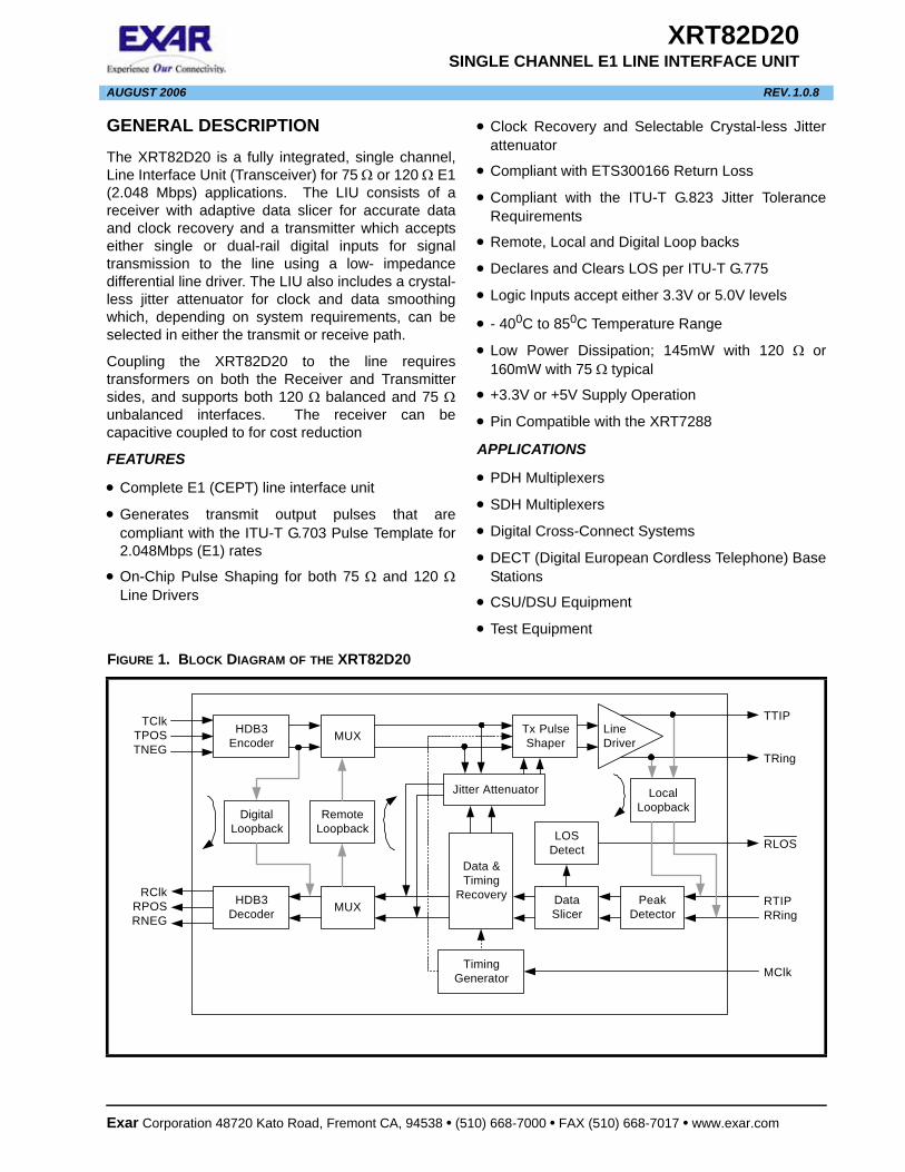
GENERAL DESCRIPTIONThe XRT82D20 is a fully integrated, single channel, Line Interface Unit (Transceiver) for 75 Ω or 120 Ω E1 (2.048 Mbps) applications. The LIU consists of a receiver with adaptive data slicer for accurate data and clock recovery and a transmitter which accepts either single or dual-rail digital inputs for signal transmission to the line using a low- impedance differential line driver. The LIU also includes a crystal-less jitter attenuator for clock and data smoothing which, depending on system requirements, can be selected in either the transmit or receive path.
Coupling the XRT82D20 to the line requires transformers on both the Receiver and Transmitter sides, and supports both 120 Ω balanced and 75 Ωunbalanced interfaces. The receiver can be capacitive coupled to for cost reduction
FEATURES
• Complete E1 (CEPT) line interface unit
• Generates transmit output pulses that are compliant with the ITU-T G.703 Pulse Template for 2.048Mbps (E1) rates
• On-Chip Pulse Shaping for both 75 Ω and 120 ΩLine Drivers
Exar Corporation 48720 Kato Road, Fremont CA, 94538 • (5
• Clock Recovery and Selectable Crystal-less Jitter attenuator
• Compliant with ETS300166 Return Loss
• Compliant with the ITU-T G.823 Jitter Tolerance Requirements
• Remote, Local and Digital Loop backs
• Declares and Clears LOS per ITU-T G.775
• Logic Inputs accept either 3.3V or 5.0V levels
• - 400C to 850C Temperature Range
• Low Power Dissipation; 145mW with 120 Ω or 160mW with 75 Ω typical
• +3.3V or +5V Supply Operation
• Pin Compatible with the XRT7288
APPLICATIONS
• PDH Multiplexers
• SDH Multiplexers
• Digital Cross-Connect Systems
• DECT (Digital European Cordless Telephone) Base Stations
• CSU/DSU Equipment
• Test Equipment
FIGURE 1. BLOCK DIAGRAM OF THE XRT82D20
HDB3Encoder
PeakDetector
LocalLoopback
LOSDetect
DataSlicer
Data &Timing
Recovery
RemoteLoopback
HDB3Decoder
DigitalLoopback
Tx PulseShaperMUX
MUX
LineDriver
TClkTPOSTNEG
RClkRPOSRNEG
TTIP
TRing
RLOS
RTIPRRing
MClkTiming
Generator
Jitter Attenuator
10) 668-7000 • FAX (510) 668-7017 • www.exar.com
XRT82D20 SINGLE CHANNEL E1 LINE INTERFACE UNIT REV. 1.0.8
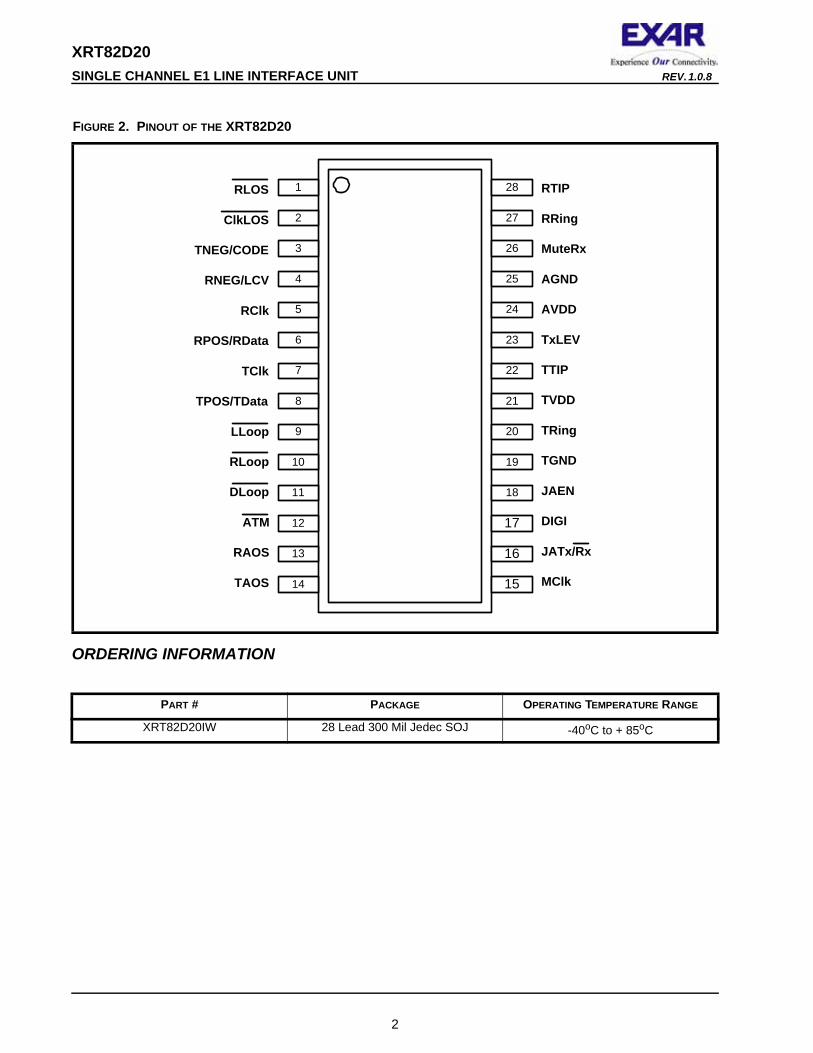
ORDERING INFORMATION
FIGURE 2. PINOUT OF THE XRT82D20
PART # PACKAGE OPERATING TEMPERATURE RANGE
XRT82D20IW 28 Lead 300 Mil Jedec SOJ -40oC to + 85oC
RLOS
ClkLOS
TNEG/CODE
RNEG/LCV
RClk
RPOS/RData
TClk
TPOS/TData
LLoop
RLoop
DLoop
ATM
RAOS
TAOS
RTIP
RRing
MuteRx
AGND
AVDD
TxLEV
TTIP
TVDD
TRing
TGND
JAEN
DIGI
JATx/Rx
MClk
1
2
9
13
12
11
10
8
7
6
5
4
3
14
28
27
20
16
17
18
19
21
22
23
24
25
26
15
2
XRT82D20REV. 1.0.8 SINGLE CHANNEL E1 LINE INTERFACE UNIT
TABLE OF CONTENTS
GENERAL DESCRIPTION................................................................................................ 1FEATURES................................................................................................................................................. 1APPLICATIONS.......................................................................................................................................... 1
FIGURE 1. BLOCK DIAGRAM OF THE XRT82D20............................................................................................................................... 1FIGURE 2. PINOUT OF THE XRT82D20............................................................................................................................................. 2
ORDERING INFORMATION .............................................................................................................................. 2TABLE OF CONTENTS ............................................................................................................ IPIN DESCRIPTIONS......................................................................................................... 3
FIGURE 3. INTERFACE TIMING DIAGRAM IN BOTH SINGLE-RAIL AND DUAL-RAIL MODE, WITH DIGI (PIN 17) = “0” ............................... 6FIGURE 4. INTERFACE TIMING DIAGRAM IN DUAL-RAIL MODE ONLY, WITH DIGI (PIN 17) = “1” ........................................................... 6
ELECTRICAL CHARACTERISTICS................................................................................. 7TABLE 1: RECEIVER CHARACTERISTICS ............................................................................................................................................ 7TABLE 2: TRANSMITTER CHARACTERISTICS ....................................................................................................................................... 7TABLE 3: 3.3V POWER CONSUMPTION INCLUDING LINE POWER DISSIPATION, TRANSMISSION AND RECEIVE PATHS ALL ACTIVE .......... 7TABLE 4: 5V POWER CONSUMPTION INCLUDING LINE POWER DISSIPATION, TRANSMISSION AND RECEIVE PATHS ALL ACTIVE ............. 8TABLE 5: AC ELECTRICAL CHARACTERISTICS .................................................................................................................................. 8TABLE 6: DC ELECTRICAL CHARACTERISTICS ................................................................................................................................... 9
ABSOLUTE MAXIMUM RATINGS.............................................................................................................. 9FIGURE 5. RECEIVER MAXIMUM JITTER TOLERANCE, TEST CONDITIONS: TEST PATTERN 215-1, (-6DB) CABLE LOSS ....................... 10FIGURE 6. RECEIVER JITTER TRANSFER FUNCTION (JITTER ATTENUATOR DISABLED), TEST CONDITIONS: TEST PATTERN 215-1, INPUT JIT-
TER 0.5UIP-P ................................................................................................................................................................ 10FIGURE 7. RECEIVER JITTER TRANSFER FUNCTION (JITTER ATTENUATOR ENABLED) TEST CONDITIONS: TEST PATTERN 215-1, INPUT JITTER
75% OF MAXIMUM JITTER TOLERANCE........................................................................................................................... 11SYSTEM DESCRIPTION................................................................................................. 121.0 THE RECEIVE SECTION....................................................................................................................... 12
1.1 JITTER ATTENUATOR ..................................................................................................................................... 121.2 THE TRANSMIT SECTION................................................................................................................................ 12
FIGURE 8. ILLUSTRATION ON HOW THE XRT82D20 SAMPLES THE DATA ON THE TPOS AND TNEG INPUT PINS ................................ 131.3 THE PULSE SHAPING CIRCUIT ...................................................................................................................... 13
FIGURE 9. ILLUSTRATION OF THE ITU-T G.703 PULSE TEMPLATE FOR E1 APPLICATION .................................................................. 141.4 INTERFACING THE TRANSMIT SECTION OF THE XRT82D20 TO THE LINE.............................................. 15
FIGURE 10. ILLUSTRATION OF HOW TO INTERFACE THE XRT82D20 TO THE LINE FOR 75 OHM APPLICATIONS AND 3.3V OPERATION ONLY 15
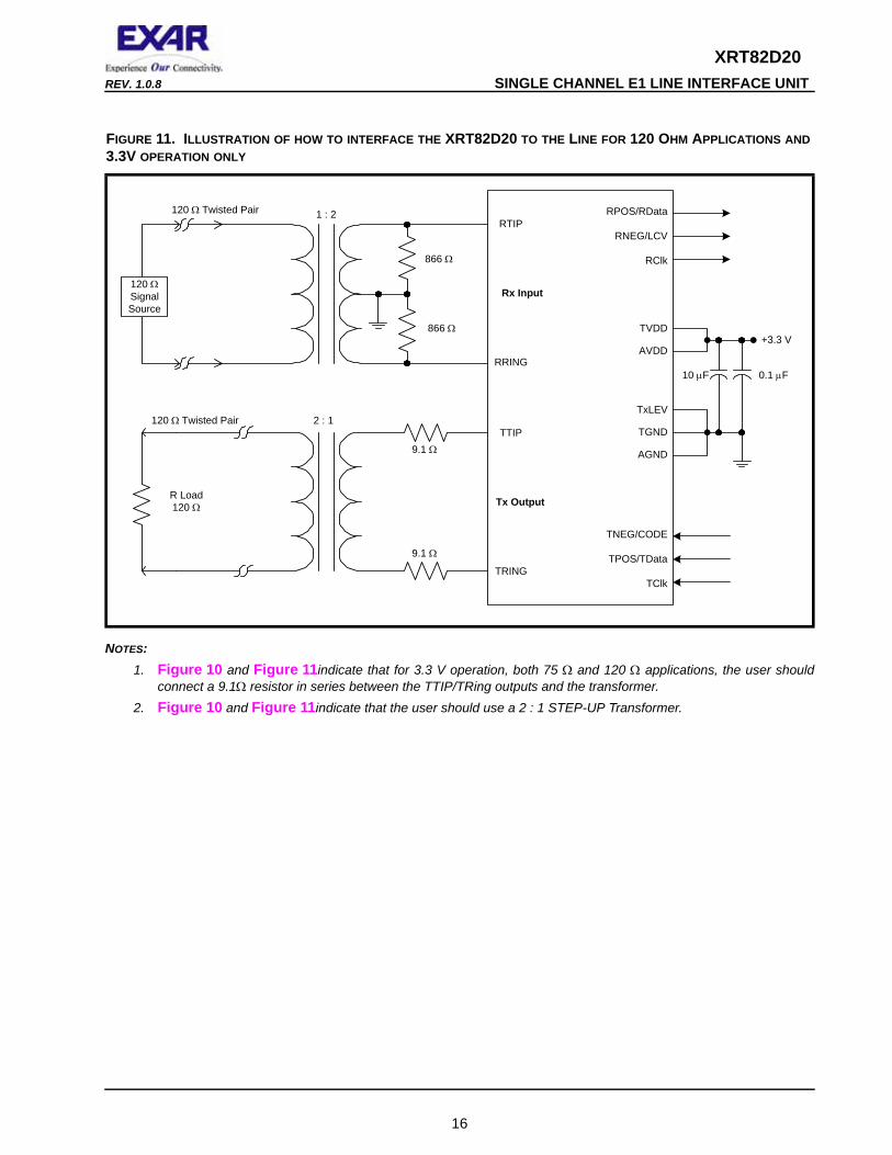
FIGURE 11. ILLUSTRATION OF HOW TO INTERFACE THE XRT82D20 TO THE LINE FOR 120 OHM APPLICATIONS AND 3.3V OPERATION ONLY 16
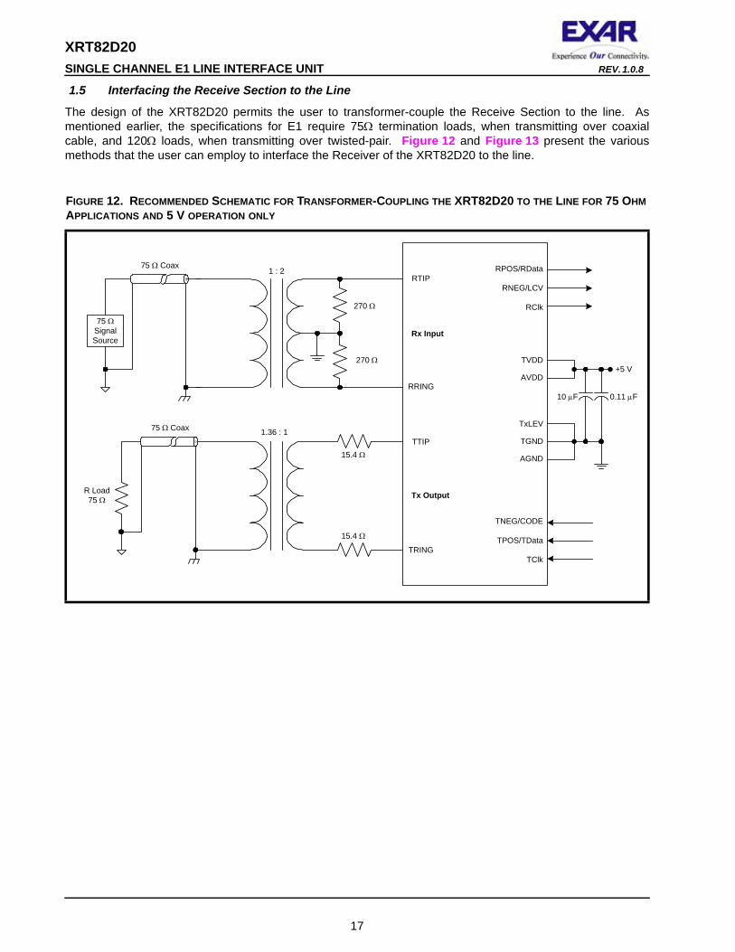
1.5 INTERFACING THE RECEIVE SECTION TO THE LINE.................................................................................. 17FIGURE 12. RECOMMENDED SCHEMATIC FOR TRANSFORMER-COUPLING THE XRT82D20 TO THE LINE FOR 75 OHM APPLICATIONS AND 5
V OPERATION ONLY ....................................................................................................................................................... 17FIGURE 13. RECOMMENDED SCHEMATIC FOR TRANSFORMER-COUPLING THE XRT82D20 TO THE LINE FOR 120 OHM APPLICATIONS AND 5
V OPERATION ONLY ....................................................................................................................................................... 181.6 CAPACITIVELY-COUPLING THE RECEIVE SECTION(S) OF THE XRT82D20 TO THE LINE...................... 19
FIGURE 14. CAPACITIVELY-COUPLING THE RECEIVE SECTION FOR 75 OHM APPLICATION AND 3.3V SUPPLY ..................................... 19FIGURE 15. CAPACITIVELY-COUPLING THE RECEIVE SECTION FOR 120 OHM APPLICATION AND 3.3V SUPPLY ................................... 20FIGURE 16. CAPACITIVELY-COUPLING THE RECEIVE SECTION FOR 75 OHM APPLICATION AND 5V SUPPLY ........................................ 21FIGURE 17. CAPACITIVELY-COUPLING THE RECEIVE SECTION FOR 120 OHM APPLICATION AND 5V SUPPLY ...................................... 22
2.0 DIAGNOSTIC FEATURES..................................................................................................................... 232.1 THE LOCAL LOOP-BACK MODE .................................................................................................................... 23
FIGURE 18. ILLUSTRATION OF THE ANALOG LOCAL LOOP-BACK WITHIN THE XRT82D20.................................................................. 232.2 THE REMOTE LOOP BACK MODE.................................................................................................................. 24
FIGURE 19. ILLUSTRATION OF THE REMOTE LOOP-BACK PATH, WITHIN THE XRT82D20................................................................... 24PACKAGE OUTLINE DRAWING.................................................................................... 25
REVISION HISTORY ..................................................................................................................................... 26
I
XRT82D20 SINGLE CHANNEL E1 LINE INTERFACE UNIT REV. 1.0.8
3
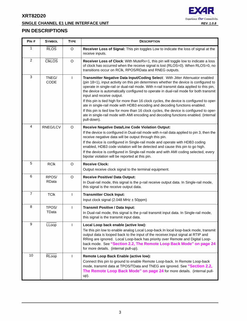
PIN DESCRIPTIONS
PIN # SYMBOL TYPE DESCRIPTION
1 RLOS O Receiver Loss of Signal: This pin toggles Low to indicate the loss of signal at the receive inputs.
2 ClkLOS O Receiver Loss of Clock: With MuteRx=1, this pin will toggle low to indicate a loss of clock has occurred when the receive signal is lost (RLOS=0). When RLOS=0, no transitions occur on RClk, RPOS/RData and RNEG outputs.
3 TNEG/CODE
I Transmitter Negative Data Input/Coding Select: With Jitter Attenuator enabled (pin 18=1), input activity on this pin determines whether the device is configured to operate in single-rail or dual-rail mode. With n-rail transmit data applied to this pin, the device is automatically configured to operate in dual-rail mode for both transmit input and receive output.If this pin is tied high for more than 16 clock cycles, the device is configured to oper-ate in single-rail mode with HDB3 encoding and decoding functions enabled.If this pin is tied low for more than 16 clock cycles, the device is configured to oper-ate in single-rail mode with AMI encoding and decoding functions enabled. (internal pull-down).
4 RNEG/LCV O Receive Negative Data/Line Code Violation Output:If the device is configured in Dual-rail mode with n-rail data applied to pin 3, then the receive negative data will be output through this pin.If the device is configured in Single-rail mode and operate with HDB3 coding enabled, HDB3 code violation will be detected and cause this pin to go high. If the device is configured in Single-rail mode and with AMI coding selected, every bipolar violation will be reported at this pin.
5 RClk O Receive Clock:Output receive clock signal to the terminal equipment.
6 RPOS/RData
O Receive Positive/ Data Output:In Dual-rail mode, this signal is the p-rail receive output data. In Single-rail mode, this signal is the receive output data.
7 TClk I Transmitter Clock Input:Input clock signal (2.048 MHz ± 50ppm)
8 TPOS/TData
I Transmit Positive / Data Input:In Dual-rail mode, this signal is the p-rail transmit input data. In Single-rail mode, this signal is the transmit input data.
9 LLoop I Local Loop back enable (active low):Tie this pin low to enable analog Local Loop-back.In local loop-back mode, transmit output data is looped back to the input of the receiver.Input signal at RTIP and RRing are ignored. Local Loop-back has priority over Remote and Digital Loop-back mode. See “Section 2.2, The Remote Loop Back Mode” on page 24 for more details. (internal pull-up).
10 RLoop I Remote Loop Back Enable (active low):Connect this pin to ground to enable Remote Loop-back. In Remote Loop-back mode, transmit data at TPOS/TData and TNEG are ignored. See “Section 2.2, The Remote Loop Back Mode” on page 24 for more details. (internal pull-up).
XRT82D20REV. 1.0.8 SINGLE CHANNEL E1 LINE INTERFACE UNIT
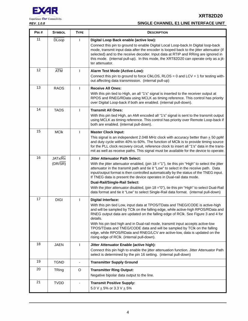
11 DLoop I Digital Loop Back enable (active low):Connect this pin to ground to enable Digital Local Loop-back.In Digital loop-back mode, transmit input data after the encoder is looped back to the jitter attenuator (if selected) and to the receive decoder. Input data at RTIP and RRing are ignored in this mode. (internal pull-up). In this mode, the XRT82D20 can operate only as a jit-ter attenuator.
12 ATM I Alarm Test Mode (Active-Low):Connect this pin to ground to force ClkLOS, RLOS = 0 and LCV = 1 for testing with-out affecting data transmission. (internal pull-up)
13 RAOS I Receive All Ones:With this pin tied to High, an all “1’s” signal is inserted to the receiver output at RPOS and RNEG/RData using MCLK as timing reference. This control has priority over Digital Loop-back if both are enabled. (internal pull-down).
14 TAOS I Transmit All Ones:With this pin tied High, an AMI encoded all “1’s” signal is sent to the transmit output using MCLK as timing reference. This control has priority over Remote Loop-back if both are enabled. (internal pull-down).
15 MClk I Master Clock Input:This signal is an independent 2.048 MHz clock with accuracy better than + 50 ppM and duty cycle within 40% to 60%. The function of MClk is to provide timing source for the PLL clock recovery circuit, reference clock to insert all “1’s” data in the trans-mit as well as receive paths. This signal must be available for the device to operate.
16 JATx/Rx(DR/SR)
I Jitter Attenuator Path Select:With the jitter attenuator enabled, (pin 18 =”1”), tie this pin “High” to select the jitter attenuator in the transmit path and tie it “Low” to select in the receive path. Data input/output format is then controlled automatically by the status of the TNEG input. If TNEG data is present the device operates in Dual-rail data mode.Dual-Rail/Single-Rail Select:With the jitter attenuator disabled, (pin 18 =”0”), tie this pin “High” to select Dual-Rail data format and tie it “Low” to select Single-Rail data format. (internal pull-down)
17 DIGI I Digital Interface:With this pin tied Low, input data at TPOS/TData and TNEG/CODE is active-high and will be sampled by TClk on the falling edge, while active-high RPOS/RData and RNEG output data are updated on the falling edge of RClk. See Figure 3 and 4 for details.With his pin tied high and in Dual-rail mode, transmit input accepts active-low TPOS/TData and TNEG/CODE data and will be sampled by TClk on the falling edge, while RPOS/RData and RNEG/LCV are active-low, data is updated on the rising edge of RClk. (internal pull-down).
18 JAEN I Jitter Attenuator Enable (active high):Connect this pin high to enable the jitter attenuation function. Jitter Attenuator Path select is determined by the pin 16 setting. (internal pull-down)
19 TGND - Transmitter Supply Ground
20 TRing O Transmitter Ring Output:Negative bipolar data output to the line.
21 TVDD - Transmit Positive Supply: 5.0 V + 5% or 3.3 V + 5%
PIN # SYMBOL TYPE DESCRIPTION
4
XRT82D20 SINGLE CHANNEL E1 LINE INTERFACE UNIT REV. 1.0.8
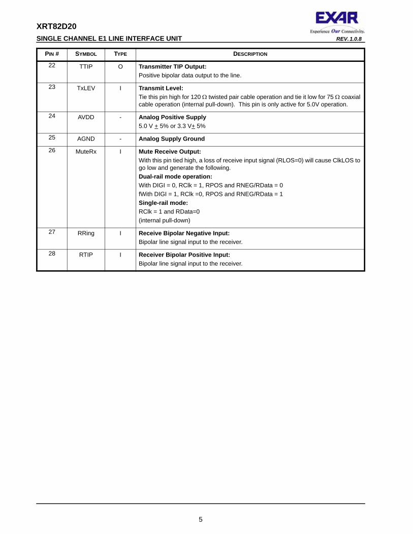
22 TTIP O Transmitter TIP Output:Positive bipolar data output to the line.
23 TxLEV I Transmit Level:Tie this pin high for 120 Ω twisted pair cable operation and tie it low for 75 Ω coaxial cable operation (internal pull-down). This pin is only active for 5.0V operation.
24 AVDD - Analog Positive Supply5.0 V + 5% or 3.3 V+ 5%
25 AGND - Analog Supply Ground
26 MuteRx I Mute Receive Output:With this pin tied high, a loss of receive input signal (RLOS=0) will cause ClkLOS to go low and generate the following.Dual-rail mode operation:With DIGI = 0, RClk = 1, RPOS and RNEG/RData = 0fWith DIGI = 1, RClk =0, RPOS and RNEG/RData = 1Single-rail mode:RClk = 1 and RData=0(internal pull-down)
27 RRing I Receive Bipolar Negative Input:Bipolar line signal input to the receiver.
28 RTIP I Receiver Bipolar Positive Input:Bipolar line signal input to the receiver.
PIN # SYMBOL TYPE DESCRIPTION
5

XRT82D20REV. 1.0.8 SINGLE CHANNEL E1 LINE INTERFACE UNIT
FIGURE 3. INTERFACE TIMING DIAGRAM IN BOTH SINGLE-RAIL AND DUAL-RAIL MODE, WITH DIGI (PIN 17) = “0”
FIGURE 4. INTERFACE TIMING DIAGRAM IN DUAL-RAIL MODE ONLY, WITH DIGI (PIN 17) = “1”
TClk
TPOS/TDataor
TNEG/CODE
Active High
Active High
RClk
RPOS/RDataor
RNEG/LCV
TClk
tr tf
tr tf
tRCD
tRSU
tRHO
tTHOtTSU
TClk
TPOS/TData Active Low
Active Low
RClk
RPOS/RData
tr tf
TClk
tTSU tTHO
tr tf
tRSU
tRHO
tRCD
6

XRT82D20 SINGLE CHANNEL E1 LINE INTERFACE UNIT REV. 1.0.8
ELECTRICAL CHARACTERISTICS
TABLE 1: RECEIVER CHARACTERISTICS
TA = 25°C, VDD = 3.3V± 5% or 5V± 5% Unless otherwise specified
PARAMETER MIN. TYP. MAX UNIT
Receiver Sensitivity 0.7 4.2 Vp
Interference Margin with -6db Cable Loss -18 -14 - dB
Input Impedance measured between RTIP or RRing to ground
0.9 2.0 - kΩ
Recovered Clock Jitter Transfer Corner FrequencyPeaking Amplitude
--
180.1
360.5
kHzdB
Jitter Attenuator Corner Frequency (-3dB curve) - 20 40 Hz
Return Loss51kHz-102kHz102kHz-2048kHz2048kHz-3072kHz
121814
253525
---
dBdBdB
TABLE 2: TRANSMITTER CHARACTERISTICS
TA = 25°C, VDD = 3.3V± 5% or 5V± 5% Unless otherwise specified
PARAMETER MIN. TYP. MAX UNIT
AMI Output Pulse Amplitude75 Ω Application120 Ω Application
2.142.70
2.373.00
2.603.30
VV
Output Pulse Width 224 244 264 ns
Output Pulse Amplitude Ratio 0.9 1.0 1.1
Jitter Added by the Transmitter Output - 0.025 0.050 UIpp
Output Return Loss:51kHz -102kHz102kHz-2048kHz2048kHz-3072kHz
---
202520
---
dBdBdB
TABLE 3: 3.3V POWER CONSUMPTION INCLUDING LINE POWER DISSIPATION, TRANSMISSION AND RECEIVE PATHS ALL ACTIVE
TA = -40° to 85°C, VDD = 3.3V± 5% Unless otherwise specified
SYMBOL
PARAMETER MIN. TYP. MAX UNIT CONDITIONS
PC Power Consumption - 100 140 mW 75Ω load, operating at 50% Mark Density
PC Power Consumption - 92 130 mW 120Ω load, operating at 50% Mark Density
PC Power Consumption - 150 190 mW 75Ω load, operating at 100% Mark Density
7

XRT82D20REV. 1.0.8 SINGLE CHANNEL E1 LINE INTERFACE UNIT
PC Power Consumption - 125 160 mW 120Ω load, operating at 100% Mark Den-sity
TABLE 4: 5V POWER CONSUMPTION INCLUDING LINE POWER DISSIPATION, TRANSMISSION AND RECEIVE PATHS ALL ACTIVE
(TA = -40° to 85°C, VDD = 5V ± 5% Unless otherwise specified)
SYMBOL
PARAMETER MIN. TYP. MAX UNIT CONDITIONS
PC Power Consumption - 160 210 mW 75Ω load, operating at 50% Mark Density
PC Power Consumption - 145 195 mW 120Ω load, operating at 50% Mark Density
PC Power Consumption - 200 260 mW 75Ω load, operating at 100% Mark Density
PC Power Consumption - 180 240 mW 120Ω load, operating at 100% Mark Den-sity
TABLE 5: AC ELECTRICAL CHARACTERISTICS
TA = -40 to +85 °C, VDD = 3.3V± 5% or 5V ± 5% Unless otherwise specified
PARAMETER SYMBOL MIN. TYP MAX UNITS
Clock Frequency MClk -50 ppm 2.048 +50ppm MHz
Clock Duty Cycle MClk 40 50 60 %
Clock Period TClk - 244 - ns
TClk Duty Cycle TCDU 30 50 70 %
Transmit Data Setup Time tTSU 40 - - ns
Transmit Data Hold Time tTHO 40 - - ns
TClk Rise Time (10% /90%) tr - - 40 ns
TClk Fall Time (90% / 10%) tf - - 40 ns
RClk Duty Cycle RCDU 45 50 55 %
Receive Data Setup Time tRSU 150 244 - ns
Receive Data Hold Time tRHO 150 244 - ns
RClk to Data Delay tRCD - - 40 ns
RClk Rise Time (10%/90%) tr - - 40 ns
RClk Fall Time (90%/10%) tf - - 40 ns
TABLE 3: 3.3V POWER CONSUMPTION INCLUDING LINE POWER DISSIPATION, TRANSMISSION AND RECEIVE PATHS ALL ACTIVE
TA = -40° to 85°C, VDD = 3.3V± 5% Unless otherwise specified
SYMBOL
PARAMETER MIN. TYP. MAX UNIT CONDITIONS
8
XRT82D20 SINGLE CHANNEL E1 LINE INTERFACE UNIT REV. 1.0.8
NOTE: All Digital output pins except pin 1 and pin 2, which typically source 20µA at VOH and sink -4mA at VOL
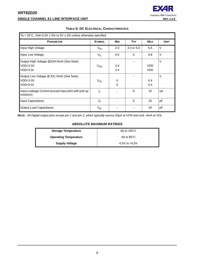
TABLE 6: DC ELECTRICAL CHARACTERISTICS
Ta = 25°C, Vdd=3.3V ± 5% or 5V ± 5% unless otherwise specified
PARAMETER SYMBOL MIN TYP MAX UNIT
Input High Voltage VIH 2.0 3.3 or 5.0 5.5 V
Input Low Voltage VIL 0.5 0 0.8 V
Output High Voltage @IOH=5mA (See Note)VDD=3.3VVDD=5.0v
VOH 2.42.4
-VDDVDD
V
Output Low Voltage @ IOL=5mA (See Note)VDD=3.3VVDD=5.0v
VOL 00
-0.40.4
V
Input Leakage Current (except input pins with pull-up resistors)
IL - 0 10 uA
Input Capacitance CI - 5 20 pF
Output Load Capacitance CO - - 20 pF
ABSOLUTE MAXIMUM RATINGS
Storage Temperature -65 to 150°C
Operating Temperature -40 to 85°C
Supply Voltage -0.5V to +5.5V
9
XRT82D20REV. 1.0.8 SINGLE CHANNEL E1 LINE INTERFACE UNIT
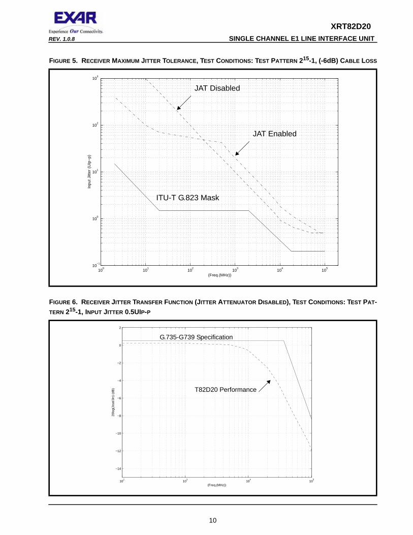
FIGURE 5. RECEIVER MAXIMUM JITTER TOLERANCE, TEST CONDITIONS: TEST PATTERN 215-1, (-6dB) CABLE LOSS
FIGURE 6. RECEIVER JITTER TRANSFER FUNCTION (JITTER ATTENUATOR DISABLED), TEST CONDITIONS: TEST PAT-TERN 215-1, INPUT JITTER 0.5UIP-P
100
101
102
103
104
105
10−1
100
101
102
103
(Freq.(MHz))
Inpu
t Jitt
er (
UIp
−p)
JAT Disabled
ITU-T G.823 Mask
JAT Enabled
102
103
104
105
−14
−12
−10
−8
−6
−4
−2
0
2
(Freq.(MHz))
20lo
g(Jo
ut/J
in)
(dB
) T82D20 Performance
G.735-G739 Specification
10
XRT82D20 SINGLE CHANNEL E1 LINE INTERFACE UNIT REV. 1.0.8
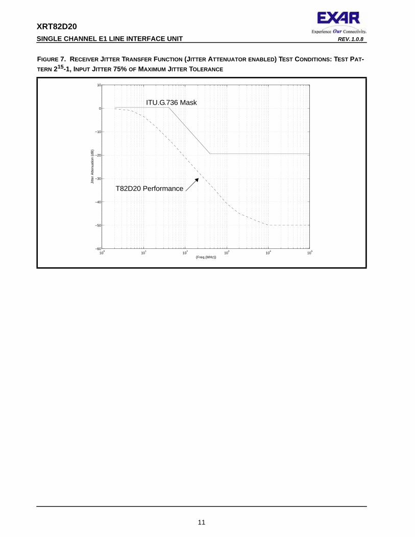
FIGURE 7. RECEIVER JITTER TRANSFER FUNCTION (JITTER ATTENUATOR ENABLED) TEST CONDITIONS: TEST PAT-TERN 215-1, INPUT JITTER 75% OF MAXIMUM JITTER TOLERANCE
100
101
102
103
104
105
−60
−50
−40
−30
−20
−10
0
10
(Freq.(MHz))
Jitte
r A
ttenu
atio
n (d
B)
T82D20 Performance
ITU.G.736 Mask
11
XRT82D20REV. 1.0.8 SINGLE CHANNEL E1 LINE INTERFACE UNIT
SYSTEM DESCRIPTIONThe XRT82D20 is a single channel E1 transceiver that provides an electrical interface for 2.048Mbps applications. XRT82D20 includes a receive circuit that converts an ITU-T G.703 compliant bipolar signal into a TTL compatible logic levels. The receiver also includes an LOS (Loss of Signal) detection circuit. Similarly, in the Transmit Direction, the Transmitter converts TTL compatible logic levels into a G.703 compatible bipolar signal.
The XRT82D20 consists of both a Receive Section, Jitter Attenuator and Transmit Section; each of these sections will be discussed below.
1.0 THE RECEIVE SECTION
At the receiver input, cable attenuated AMI signal can be coupled to the receiver using a capacitor or transformer. The receive data first goes through the peak detector and data slicer for accurate data recovery.The digital representation of the AMI signals go to the clock recovery circuit for timing recovery and subsequently to the decoder (if selected) for HDB3 decoding before being output to the RPOS/RData and RNEG/LCV pins. The digital data output can be in NRZ or RZ format depending the mode of operation selected and with the option to be in dual-rail or single rail mode. Clock timing recovery of the line interface is accomplished by means of a digital PLL scheme which has high input jitter tolerance.
The purpose of the Receive Output Interface block is to interface directly with the Receiving Terminal Equipment. The Receive Output Interface block outputs the data (which has been recovered from the incoming line signal) to the Receive Terminal Equipment via the RPOS and RNEG output pins.
If the Receive Section of the XRT82D20 has received a Positive-Polarity pulse, via the RTIP and
RRing input pins, then the Receive Output Interface will output a pulse at the RPOS output pin.
Similarly, if the Receive Section of the XRT82D20 has received a Negative-Polarity pulse, via the RTIP and RRing input pins, then the Receive Output Interface will output a pulse at the RNEG output pin.
1.1 JITTER ATTENUATOR
To reduce frequency jitter in the transmit clock or receive clock, a crystal-less jitter attenuator is provided. The jitter attenuator can be selected either in the transmit or receive path or it can be disabled.
1.2 THE TRANSMIT SECTION
In general, the purpose of the Transmit Section (within the XRT82D20) is to accept TTL/CMOS level digital data (from the Terminal Equipment), and to encode it into a format such that it can:1. Be efficiently transmitted over coaxial- or twisted pair cable at the E1 data rate; and 2. Be reliably received by the Remote Terminal Equipment at the other end of the E1 data link.3. Comply with the ITU-T G.703 pulse template requirements, for E1 applications
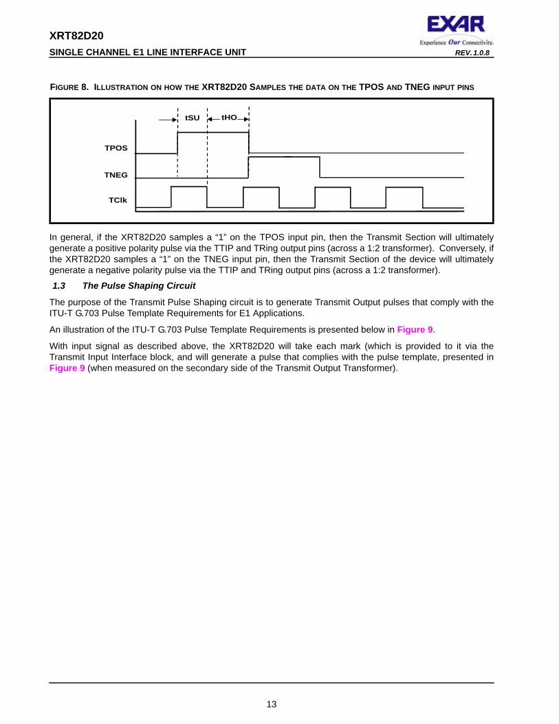
A 2.048 MHz clock is applied to the TClk input pin and NRZ data at the TPOS and TNEG input pins. The Transmit Input Interface circuit will sample the data, at the TPOS and TNEG input pins, upon the falling edge of TClk, as illustrated in Figure 8 below.
12
XRT82D20 SINGLE CHANNEL E1 LINE INTERFACE UNIT REV. 1.0.8
In general, if the XRT82D20 samples a “1” on the TPOS input pin, then the Transmit Section will ultimately generate a positive polarity pulse via the TTIP and TRing output pins (across a 1:2 transformer). Conversely, if the XRT82D20 samples a “1” on the TNEG input pin, then the Transmit Section of the device will ultimately generate a negative polarity pulse via the TTIP and TRing output pins (across a 1:2 transformer).
1.3 The Pulse Shaping Circuit
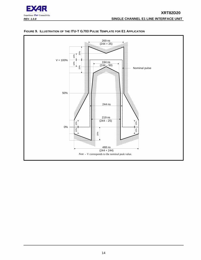
The purpose of the Transmit Pulse Shaping circuit is to generate Transmit Output pulses that comply with the ITU-T G.703 Pulse Template Requirements for E1 Applications.
An illustration of the ITU-T G.703 Pulse Template Requirements is presented below in Figure 9.
With input signal as described above, the XRT82D20 will take each mark (which is provided to it via the Transmit Input Interface block, and will generate a pulse that complies with the pulse template, presented in Figure 9 (when measured on the secondary side of the Transmit Output Transformer).
FIGURE 8. ILLUSTRATION ON HOW THE XRT82D20 SAMPLES THE DATA ON THE TPOS AND TNEG INPUT PINS
TClk
TPOS
TNEG
tSU tHO
13
XRT82D20REV. 1.0.8 SINGLE CHANNEL E1 LINE INTERFACE UNIT
FIGURE 9. ILLUSTRATION OF THE ITU-T G.703 PULSE TEMPLATE FOR E1 APPLICATION
10%
10%
10%
10%
10%
10%
269 ns(244 + 25)
194 ns(244 – 50)
244 ns
219 ns(244 – 25)
488 ns(244 + 244)
0%
50%
20%
V = 100%
Nominal pulse
Note – V corresponds to the nominal peak value.
20%
20%
14

XRT82D20 SINGLE CHANNEL E1 LINE INTERFACE UNIT REV. 1.0.8
1.4 Interfacing the Transmit Section of the XRT82D20 to the Line
ITU-T G.703 specifies that the E1 line signal can be transmitted over coaxial cable and terminated with 75Ω or transmitted over twisted-pair and terminated with 120Ω.
In both applications (e.g., 75Ω or 120Ω, the user is advised to interface the Transmitter to the Line, in the manner as depicted in Figure 10 and Figure 11, respectively.
FIGURE 10. ILLUSTRATION OF HOW TO INTERFACE THE XRT82D20 TO THE LINE FOR 75 OHM APPLICATIONS AND 3.3V OPERATION ONLY
R Load75 Ω
270 Ω
270 Ω
9.1 Ω
9.1 Ω
1 : 2
2 : 1
RTIP
RRING
TTIP
TRING
+3.3 V
0.1 µF
TVDD
AVDD
TxLEV
TNEG/CODE
TPOS/TData
TClk
RPOS/RData
RNEG/LCV
RClk
AGND
TGND
10µF
Rxx Input
Tx Output
75 Ω Coax
75 Ω Coax
75 ΩSignalSource
15
XRT82D20REV. 1.0.8 SINGLE CHANNEL E1 LINE INTERFACE UNIT
NOTES:1. Figure 10 and Figure 11indicate that for 3.3 V operation, both 75 Ω and 120 Ω applications, the user should
connect a 9.1Ω resistor in series between the TTIP/TRing outputs and the transformer.2. Figure 10 and Figure 11indicate that the user should use a 2 : 1 STEP-UP Transformer.
FIGURE 11. ILLUSTRATION OF HOW TO INTERFACE THE XRT82D20 TO THE LINE FOR 120 OHM APPLICATIONS AND 3.3V OPERATION ONLY
866 Ω
866 Ω
R Load120 Ω
9.1 Ω
9.1 Ω
1 : 2
2 : 1
RTIP
RRING
TTIP
TRING
+3.3 V
0.1 µF
TVDD
AVDD
TxLEV
TNEG/CODE
TPOS/TData
TClk
RPOS/RData
RNEG/LCV
RClk
AGND
TGND
10 µF
120 Ω Twisted Pair
120 ΩSignalSource
120 Ω Twisted Pair
Rx Input
Tx Output
16
XRT82D20 SINGLE CHANNEL E1 LINE INTERFACE UNIT REV. 1.0.8
1.5 Interfacing the Receive Section to the Line
The design of the XRT82D20 permits the user to transformer-couple the Receive Section to the line. As mentioned earlier, the specifications for E1 require 75Ω termination loads, when transmitting over coaxial cable, and 120Ω loads, when transmitting over twisted-pair. Figure 12 and Figure 13 present the various methods that the user can employ to interface the Receiver of the XRT82D20 to the line.
FIGURE 12. RECOMMENDED SCHEMATIC FOR TRANSFORMER-COUPLING THE XRT82D20 TO THE LINE FOR 75 OHM APPLICATIONS AND 5 V OPERATION ONLY
270 Ω
270 Ω
15.4 Ω
15.4 Ω
1 : 2
1.36 : 1
RTIP
RRING
TTIP
TRING
+5 V
0.11 µF
TVDD
AVDD
TxLEV
TNEG/CODE
TPOS/TData
TClk
RPOS/RData
RNEG/LCV
RClk
AGND
TGND
10 µF
R Load75 Ω
75 Ω Coax
75 Ω Coax
75 ΩSignalSource
Rx Input
Tx Output
17
XRT82D20REV. 1.0.8 SINGLE CHANNEL E1 LINE INTERFACE UNIT
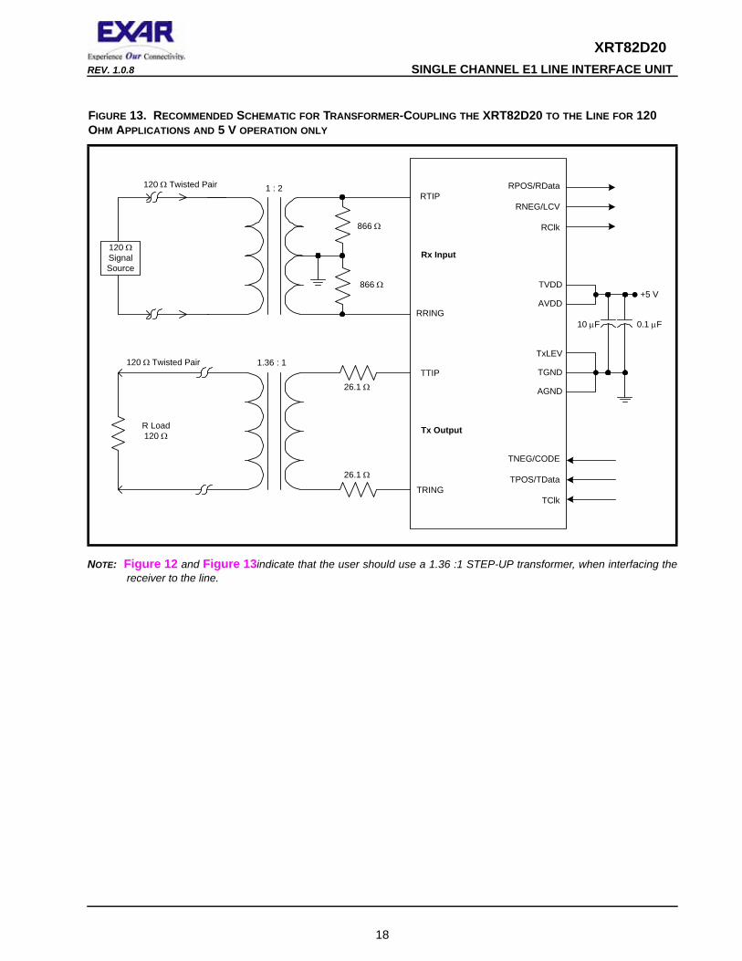
NOTE: Figure 12 and Figure 13indicate that the user should use a 1.36 :1 STEP-UP transformer, when interfacing the receiver to the line.
FIGURE 13. RECOMMENDED SCHEMATIC FOR TRANSFORMER-COUPLING THE XRT82D20 TO THE LINE FOR 120 OHM APPLICATIONS AND 5 V OPERATION ONLY
866 Ω
866 Ω
26.1 Ω
26.1 Ω
1 : 2
1.36 : 1
RTIP
RRING
TTIP
TRING
+5 V
0.1 µF
TVDD
AVDD
TxLEV
TNEG/CODE
TPOS/TData
TClk
RPOS/RData
RNEG/LCV
RClk
AGND
TGND
10 µF
R Load120 Ω
120 Ω Twisted Pair
120 ΩSignalSource
120 Ω Twisted Pair
Tx Output
Rx Input
18
XRT82D20 SINGLE CHANNEL E1 LINE INTERFACE UNIT REV. 1.0.8
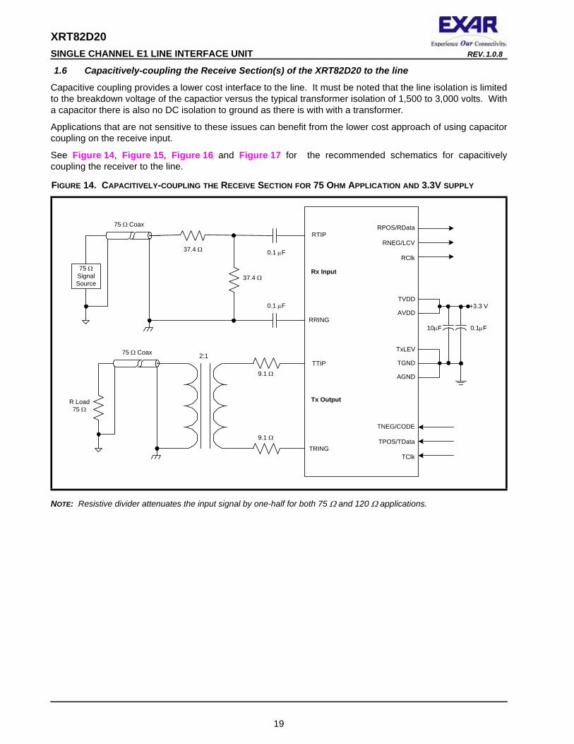
1.6 Capacitively-coupling the Receive Section(s) of the XRT82D20 to the line
Capacitive coupling provides a lower cost interface to the line. It must be noted that the line isolation is limited to the breakdown voltage of the capactior versus the typical transformer isolation of 1,500 to 3,000 volts. With a capacitor there is also no DC isolation to ground as there is with with a transformer.
Applications that are not sensitive to these issues can benefit from the lower cost approach of using capacitor coupling on the receive input.
See Figure 14, Figure 15, Figure 16 and Figure 17 for the recommended schematics for capacitively coupling the receiver to the line.
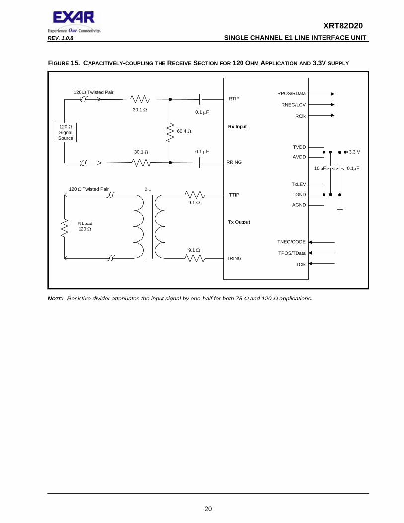
NOTE: Resistive divider attenuates the input signal by one-half for both 75 Ω and 120 Ω applications.
FIGURE 14. CAPACITIVELY-COUPLING THE RECEIVE SECTION FOR 75 OHM APPLICATION AND 3.3V SUPPLY
R Load75 Ω
75 Ω Coax
75 Ω Coax
75 ΩSignalSource
37.4 Ω
37.4 Ω
9.1 Ω
9.1 Ω
2:1
RTIP
RRING
TTIP
TRING
+3.3 V
0.1µF
TVDD
AVDD
TxLEV
TNEG/CODE
TPOS/TData
TClk
RPOS/RData
RNEG/LCV
RClk
AGND
TGND
10µF
Rx Input
Tx Output
0.1 µF
0.1 µF
19
XRT82D20REV. 1.0.8 SINGLE CHANNEL E1 LINE INTERFACE UNIT
NOTE: Resistive divider attenuates the input signal by one-half for both 75 Ω and 120 Ω applications.
FIGURE 15. CAPACITIVELY-COUPLING THE RECEIVE SECTION FOR 120 OHM APPLICATION AND 3.3V SUPPLY
30.1 Ω
60.4 Ω
9.1 Ω
9.1 Ω
2:1
RTIP
RRING
TTIP
TRING
+3.3 V
0.1µF
TVDD
AVDD
TxLEV
TNEG/CODE
TPOS/TData
TClk
RPOS/RData
RNEG/LCV
RClk
AGND
TGND
10 µF
Rx Input
Tx Output
0.1 µF
0.1 µF30.1 Ω
R Load120 Ω
120 Ω Twisted Pair
120 ΩSignalSource
120 Ω Twisted Pair
20
XRT82D20 SINGLE CHANNEL E1 LINE INTERFACE UNIT REV. 1.0.8
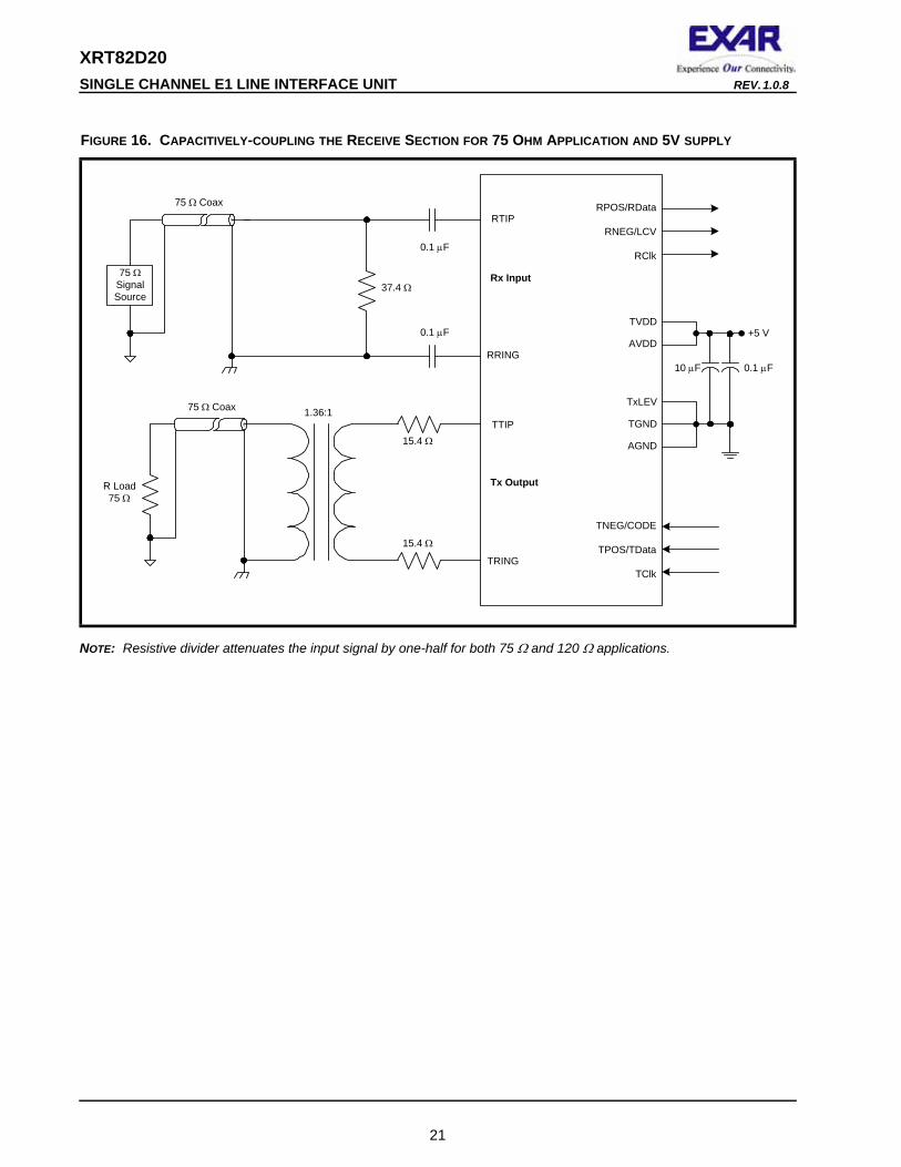
NOTE: Resistive divider attenuates the input signal by one-half for both 75 Ω and 120 Ω applications.
FIGURE 16. CAPACITIVELY-COUPLING THE RECEIVE SECTION FOR 75 OHM APPLICATION AND 5V SUPPLY
R Load75 Ω
75 Ω Coax
75 Ω Coax
75 ΩSignalSource
37.4 Ω
15.4 Ω
15.4 Ω
1.36:1
RTIP
RRING
TTIP
TRING
+5 V
0.1 µF
TVDD
AVDD
TxLEV
TNEG/CODE
TPOS/TData
TClk
RPOS/RData
RNEG/LCV
RClk
AGND
TGND
10 µF
Rx Input
Tx Output
0.1 µF
0.1 µF
21
XRT82D20REV. 1.0.8 SINGLE CHANNEL E1 LINE INTERFACE UNIT
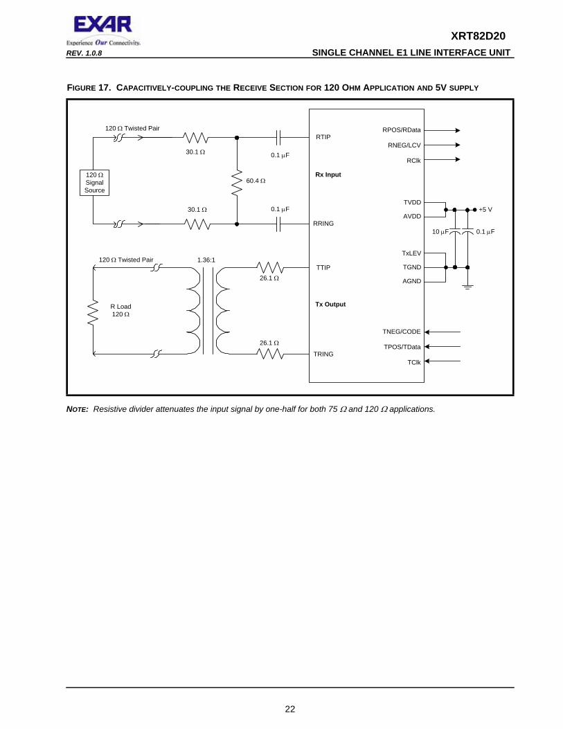
NOTE: Resistive divider attenuates the input signal by one-half for both 75 Ω and 120 Ω applications.
FIGURE 17. CAPACITIVELY-COUPLING THE RECEIVE SECTION FOR 120 OHM APPLICATION AND 5V SUPPLY
30.1 Ω
60.4 Ω
26.1 Ω
26.1 Ω
1.36:1
RTIP
RRING
TTIP
TRING
+5 V
0.1 µF
TVDD
AVDD
TxLEV
TNEG/CODE
TPOS/TData
TClk
RPOS/RData
RNEG/LCV
RClk
AGND
TGND
10 µF
Rx Input
Tx Output
0.1 µF
0.1 µF30.1 Ω
R Load120 Ω
120 Ω Twisted Pair
120 ΩSignalSource
120 Ω Twisted Pair
22
XRT82D20 SINGLE CHANNEL E1 LINE INTERFACE UNIT REV. 1.0.8
2.0 DIAGNOSTIC FEATURES
In order to support diagnostic operations, the XRT82D20 supports the following loop-back modes:
• Local Loopback
• Remote Loopback
• Digital Loopback
Each of these loop-back modes will be discussed below.
2.1 The Local Loop-Back Mode
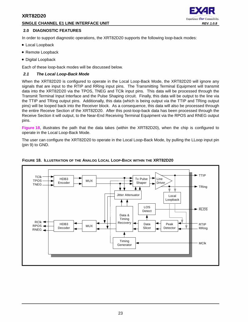
When the XRT82D20 is configured to operate in the Local Loop-Back Mode, the XRT82D20 will ignore any signals that are input to the RTIP and RRing input pins. The Transmitting Terminal Equipment will transmit data into the XRT82D20 via the TPOS, TNEG and TClk input pins. This data will be processed through the Transmit Terminal Input Interface and the Pulse Shaping circuit. Finally, this data will be output to the line via the TTIP and TRing output pins. Additionally, this data (which is being output via the TTIP and TRing output pins) will be looped back into the Receiver block. As a consequence, this data will also be processed through the entire Receive Section of the XRT82D20. After this post-loop-back data has been processed through the Receive Section it will output, to the Near-End Receiving Terminal Equipment via the RPOS and RNEG output pins.
Figure 18, illustrates the path that the data takes (within the XRT82D20), when the chip is configured to operate in the Local Loop-Back Mode.
The user can configure the XRT82D20 to operate in the Local Loop-Back Mode, by pulling the LLoop input pin (pin 9) to GND.
FIGURE 18. ILLUSTRATION OF THE ANALOG LOCAL LOOP-BACK WITHIN THE XRT82D20
HDB3Encoder
PeakDetector
LocalLoopback
LOSDetect
DataSlicer
Data &Timing
RecoveryHDB3Decoder
Tx PulseShaperMUX
MUX
LineDriver
TClkTPOSTNEG
RClkRPOSRNEG
TTIP
TRing
RLOS
RTIPRRing
MClkTiming
Generator
Jitter Attenuator
23

XRT82D20REV. 1.0.8 SINGLE CHANNEL E1 LINE INTERFACE UNIT
2.2 The Remote Loop Back Mode
When the XRT82D20 is configured to operate in the Remote Loop-Back Mode, the XRT82D20 will ignore any signals that are input to the TPOS and TNEG input pins. The XRT82D20 will receive the incoming line signals, via the RTIP and RRing input pins. This data will be processed through the entire Receive Section (within the XRT82D20) and will output to the Receive Terminal Equipment via the RPOS and RNEG output pins. Additionally, this data will also be internally looped back to the Transmit Input Interface block within the Transmit Section. At this point, this data will be routed through the remainder of the Transmit Section of the XRT82D20 and will be transmitted out onto the line via the TTIP and TRing output pins.
Figure 19, illustrates the path that the data takes (within the XRT82D20) when the chip is configured to operate in the Remote Loop-Back Mode.
NOTE: During Remote Loop-Back operation, any data which is input via the RTIP and RRING input pins, will also be output to the Terminal Equipment, via the RPOS and RNEG output pins.
FIGURE 19. ILLUSTRATION OF THE REMOTE LOOP-BACK PATH, WITHIN THE XRT82D20
HDB3Encoder
PeakDetector
LOSDetect
DataSlicer
Data &Timing
Recovery
RemoteLoopback
HDB3Decoder
Tx PulseShaperMUX
MUX
LineDriver
TClkTPOSTNEG
RClkRPOSRNEG
TTIP
TRing
RLOS
RTIPRRing
MClkTiming
Generator
Jitter Attenuator
24
XRT82D20 SINGLE CHANNEL E1 LINE INTERFACE UNIT REV. 1.0.8
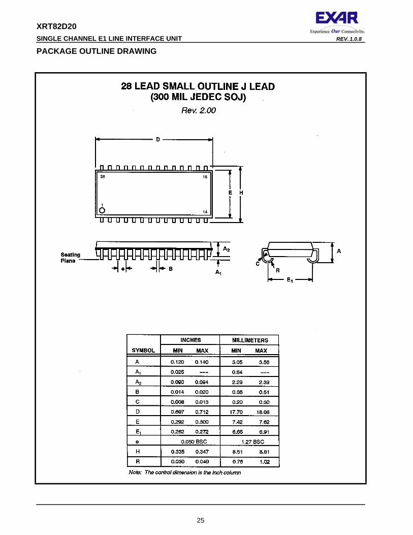
PACKAGE OUTLINE DRAWING
25
XRT82D20REV. 1.0.8 SINGLE CHANNEL E1 LINE INTERFACE UNIT
REVISION HISTORY
Rev. 1.0.6 corrections to figures, remove values from pull-up/down resistors, correct formating of ±.
Rev. 1.0.7 Minor edits of figures and text. Added 4 new figures 14, 15, 16 and 17, showing capacitive coupling of the receiver to the line.
Rev. 1.0.8 Edit Pin 9 and 10 as internal pull-up. Updated new format with new Exar logo.
26
NOTICE
EXAR Corporation reserves the right to make changes to the products contained in this publication in order to improve design, performance or reliability. EXAR Corporation assumes no responsibility for the use of any circuits described herein, conveys no license under any patent or other right, and makes no representation that the circuits are free of patent infringement. Charts and schedules contained here in are only for illustration purposes and may vary depending upon a user’s specific application. While the information in this publication has been carefully checked; no responsibility, however, is assumed for inaccuracies.
EXAR Corporation does not recommend the use of any of its products in life support applications where the failure or malfunction of the product can reasonably be expected to cause failure of the life support system or to significantly affect its safety or effectiveness. Products are not authorized for use in such applications unless EXAR Corporation receives, in writing, assurances to its satisfaction that: (a) the risk of injury or damage has been minimized; (b) the user assumes all such risks; (c) potential liability of EXAR Corporation is adequately protected under the circumstances.
Copyright 2006 EXAR Corporation
Datasheet August 2006.
Reproduction, in part or whole, without the prior written consent of EXAR Corporation is prohibited.


![Vision-Based Relative Navigation and Control for Autonomous … · American Institute of Aeronautics and Astronautics 3 with [ ] T m mx my mz ω = ω ω ω denoting the inspector](https://img.pdfslide.us/doc/110x75/5e7e173347cbfc4ede6f064a/vision-based-relative-navigation-and-control-for-autonomous-american-institute-of.jpg)

![NATURAL SCIENCES D568/12 ADMISSIONS ASSESSMENT 40 … · Ω, 2 Ω, 4 Ω, 8 Ω, 16 Ω, 32 Ω, 64 Ω, … connected in parallel with the cell. ... [2 marks] Answer: ... is used as the](https://img.pdfslide.us/doc/110x75/5f2363f7b03d7e4ce06bc15b/natural-sciences-d56812-admissions-assessment-40-2-4-8-16-32.jpg)