Embed Size (px)
Citation preview
High Power Modular Drive System
Hongyang Zhang
Master Thesis
Supervisor
Yujing Liu (ABB)
Examiner
Hans-Peter Nee (KTH)
Royal Institute of Technology (KTH)
School of Electrical Engineering
Department of Electrical Machines and Power Electronics
Stockholm 2010

XR-EE-EME 2010 :008
Author: Hongyang Zhang
Title: High Power Modular Drive System
School: Royal Institute of Technology (KTH)
Date: November 2010
Type: MastersThesis

Abstract
The novel converter topology 'Cascaded Cell Commutated drive' (CCC drive) of the brushless
DC machine for the medium voltage, high power application is investigated in this report.
Because of DC machine's good speed response and high power density, the study has been
devoted to investigate the feasibility of using the electronically commutated DC machine for
the high power (>20MW) applications where AC drives are exclusively used. The
conventional DC machines with brushes are not considered in this thesis work, since we are
aiming to develop the novel converter topology to replace the brushes with the electronic
commutator to achieve the current commutation in the coils of the machine.
During the thesis work, the coupling simulation between two software is used in order to
obtain a better comprehension of the novel converter concept, different topologies and
switching strategies of the converter are tested by the simulation, the power losses calculation
of the converters and the evaluation of the system design are given afterwards.
It was concluded that the proposed converter circuit for the CCC drive system works for the
coil current commutation and some of its important features such as high power density,
cascaded/parallel modular topology, extra low switching losses, integrated machine and
converter system make it feasible to compete or replace with the medium voltage AC drives
in the future.
Key Words: CCC drive, brushless DC , coil current commutation , converter topology

Abstrakt
Romanen omvandlare topologin "Kaskad Cell kommuterade drive" (CCC-enhet) av borstlösa DC
maskinen för mellanspänning, är hög effekt tillämpning undersöks i denna rapport.
På grund av DC maskinens bra fart respons och hög effekttäthet, har studien ägnats att undersöka
möjligheten att använda elektroniskt kommuterade DC maskin för hög effekt (> 20 MW)
applikationer där frekvensomriktare uteslutande används. Den konventionella DC-maskiner med
borstar anses inte i detta examensarbete, eftersom vi siktar på att utveckla topologi nya
omvandlaren för att ersätta borstar med den elektroniska kommutatorn att uppnå den ström
förvandling i rullar av maskinen.
Under examensarbetet är kopplingen simulering mellan två program som används för att få en
bättre förståelse av romanen omvandlare konceptet är olika topologier och koppling strategier hos
omvandlaren provas av simulering, makten förluster beräkningen av konverterare och utvärdering
av systemets konstruktion ges efteråt.
Det var slutsatsen att den föreslagna omvandlare krets för CCC drivsystemet arbetar för
spolström kommutering och några av dess viktiga funktioner som hög effekttäthet,
kaskadkopplade / parallell modulära topologi, extra låga förluster växling, integrerad maskin och
omvandlare systemet gör det möjligt att konkurrera eller ersätta med AC-drivsystem i framtiden.
Nyckelord: CCC, friktionsfri DC, spolström förvandling, omvandlare topologi

Acknowledgements
This thesis report was written for my Master of Science degree in Electric Power Engineering
at Royal Institute of Technology (KTH), the thesis work was carried out from January 14th to
the end of June at ABB Corporate Research in Västerås, Sweden (SECRC).
Firstly I wish to express my gratitude to my master thesis supervisor Dr. Yujing Liu, without
him I would not have the chance to work in ABB SECRC and I am thankful to his helpful
support, inspiration during my thesis work, although he was very busy for his work, he could
always take time to come to my place for help and whenever I had a question he could always
try to help me to solve it.
I need to say thank you to my thesis co-supervisor Dr. Pierluigi Tenca, for his profound
knowledge of the motor drive system and his excellent programming skills helped me a lot
during the thesis work. I am very thankful to Dr. Robert Chin, the group manager, for his
encouraging and support during my thesis work.
I also need to thank Dr. Rahul Kanchan, for his answers to my questions and feedbacks on my
work.
I would also like to give my special thanks to Kai Pietilaeinen in CHIND for his great help on
the ABB MV drive and Johan Lampinen in DC Machines for his study trip invitation and
valuable discussions with factory experts on the topic.
At KTH, I also owe my thanks to my master thesis supervisor and examiner Prof. Hans-Peter
Nee for his valuable help during my thesis work.
I would like to say thank you to all of my friends in Sweden, who ever helped me in the past
two years.
Last but now least, a deeply appreciation is given to my family for supporting me to study
abroad and their concerns about my life all these years. Hongyang Zhang
Västerås, Sweden
June 2010
TABLE OF CONTENTS
Abstract
Acknowledgement
1 INTRODUCTION .................................................................................................................. 1
1.1 BACKGROUND .................................................................................................................... 1
1.2 PURPOSE ............................................................................................................................. 4
1.3 SCOPE ................................................................................................................................. 4
1.4 STRUCTURE ......................................................................................................................... 4
2 LITERATURE SURVEY ...................................................................................................... 6
2.1 TRADITIONAL BLDC TOPOLOGY ......................................................................................... 6
2.2 MULTI-PHASE BLDC TOPOLOGY .......................................................................................... 6
2.3 CONCLUSIONS FOR THE LITERATURE SURVEY ................................................................... 13
3 PROPOSED CONVERTER TOPOLOGY ........................................................................ 14
3.1 SIMULATION SOFTWARE .................................................................................................... 14
3.2 PROPOSED CONVERTER TOPOLOGY ................................................................................... 16
4 SIMULATION RESULTS AND ANALYSIS .................................................................... 20
4.1 SINGLE CELL SYSTEM ........................................................................................................ 20
4.2 6-CELL SYSTEM WITH CURRENT SOURCE ........................................................................... 21
4.3 6-CELL SYSTEM WITH VOLTAGE SOURCE ........................................................................... 28
4.4 6-CELL SYSTEM WITH RECTIFIER ....................................................................................... 30
4.5 6-CELL SYSTEM WITH ADJUSTABLE SPEED ......................................................................... 33
4.6 24-CELL SYSTEM FOR HIGHER POWER ............................................................................... 34
4.7 SIMULATION FOR THE CONVERTER CIRCUIT UNDER AMATURE REACTION ......................... 37
5 POWER LOSSES IN CCC CONVERTER ....................................................................... 40
5.1 INTRODUCTION ................................................................................................................. 40
5.2 IGBT CONDUCTION LOSSES ................................................................................................ 41
5.3 DIODE CONDUCTION LOSSES ............................................................................................. 44
5.4 IGBT SWITCHING LOSSES ................................................................................................... 46
5.5 FEASIBILITY FOR IGCT- IGCT POWER LOSSES ..................................................................... 50
5.6 POWER LOSSES IN THE MULTI-CELL CIRCUIT ..................................................................... 51
6 SYSTEM DESIGN SPECIFICATION ............................................................................... 52
6.1 SYSTEM DIAGRAM ............................................................................................................. 52
6.2 COMPONENT LIST .............................................................................................................. 53
6.3 CONVERTER-MACHINE INTEGRATION ................................................................................ 56
6.4 BENCHMARKING WITH ABB'S ACS 6000 AND MEGADRIVE-LCI ........................................... 58
7 CONCLUSIONS AND FUTURE WORK .......................................................................... 62
REFERENCE .............................................................................................................................. 63
APPENDIX A .............................................................................................................................. 64
APPENDIX B ............................................................................................................................... 66
APPENDIX C .............................................................................................................................. 72
1
1 INTRODUCTION
1.1 BACKGROUND
Currently, the market for the high power, medium voltage (MV) drive has been dominated by the AC
drives, where the multi-level topology is used to produce the near-sinusoidal waveforms; hence many
research activities have been devoted on how to achieve the ideal waveform by applying more levels
or novel topologies of power electronic converters.
The typical converter topologies (load-side inverters) used for MV drive system feeding the AC
motors can be generally divided into three categories: [1]
Voltage-Source Inverters (VSIs): Now the medium voltage VSI is mainly based on the multi-
level topology and VSI can be basically divided into two categories: converters in a delta
connection and converters in a start connection.
The 3L-NPC (IGBT or IGCT based) and 4L-FC (IGBT based) shown in Figure 1-1 are typical
examples for delta-connected converters.
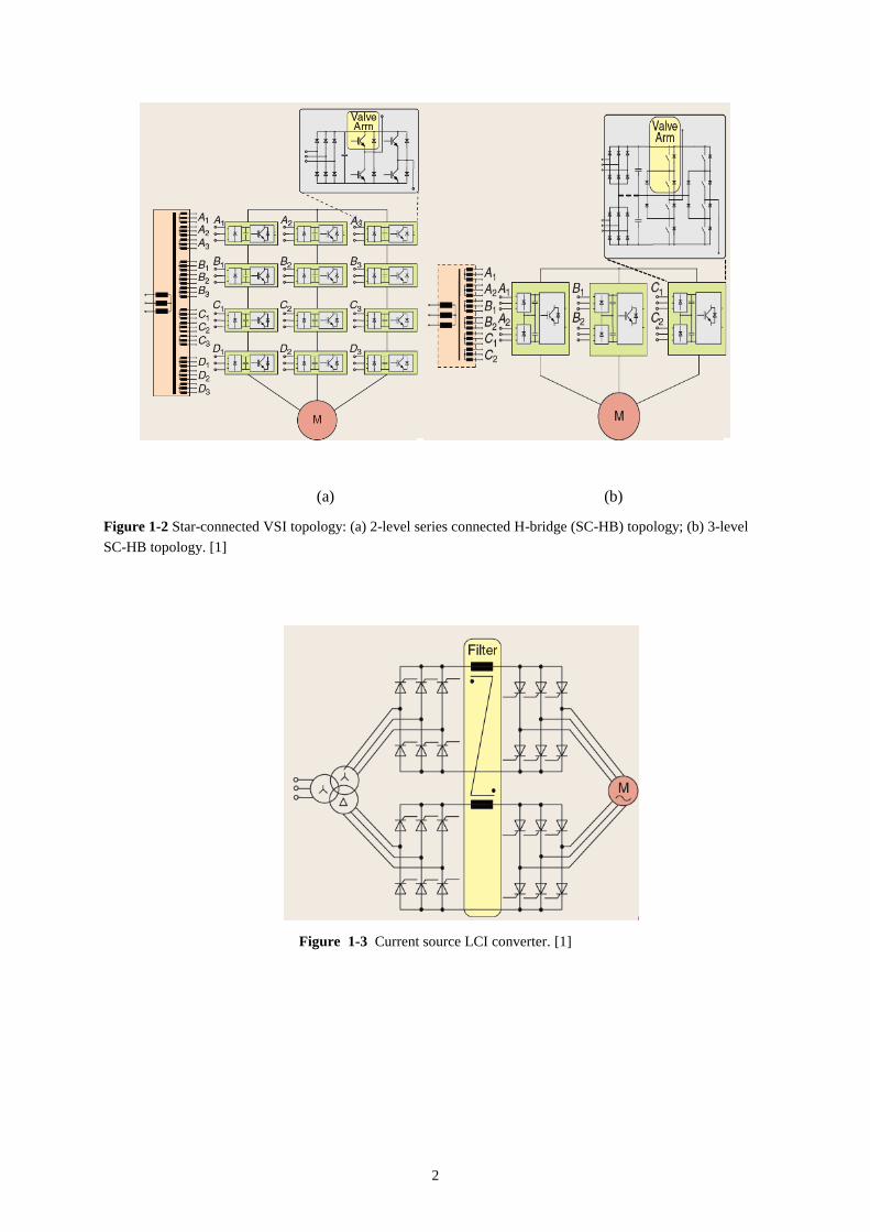
Figure 1-2 shows the star-connected VSIs which are based on the series connected H-bridge
cellular converter with 2-level or 3-level H-bridges.
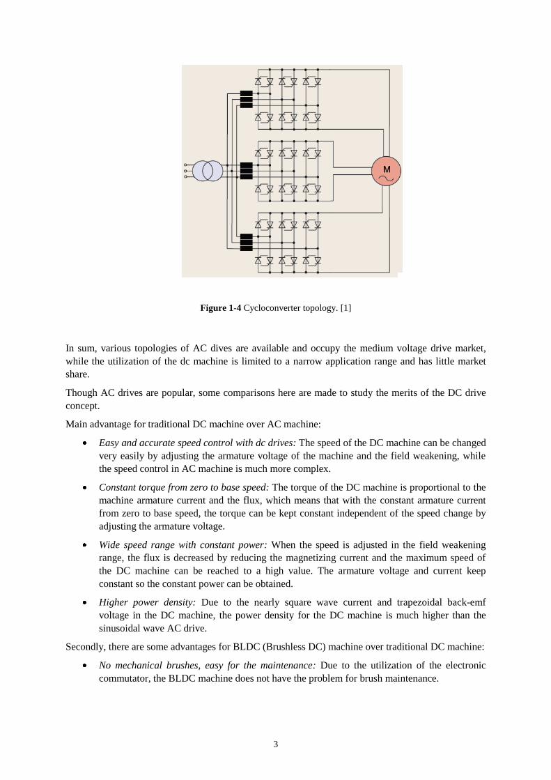
Current-Source Inverters (CSIs): Load Commutated Inverters (LCI) for high power
application (>20MW). The topology is shown in Figure 1-3.
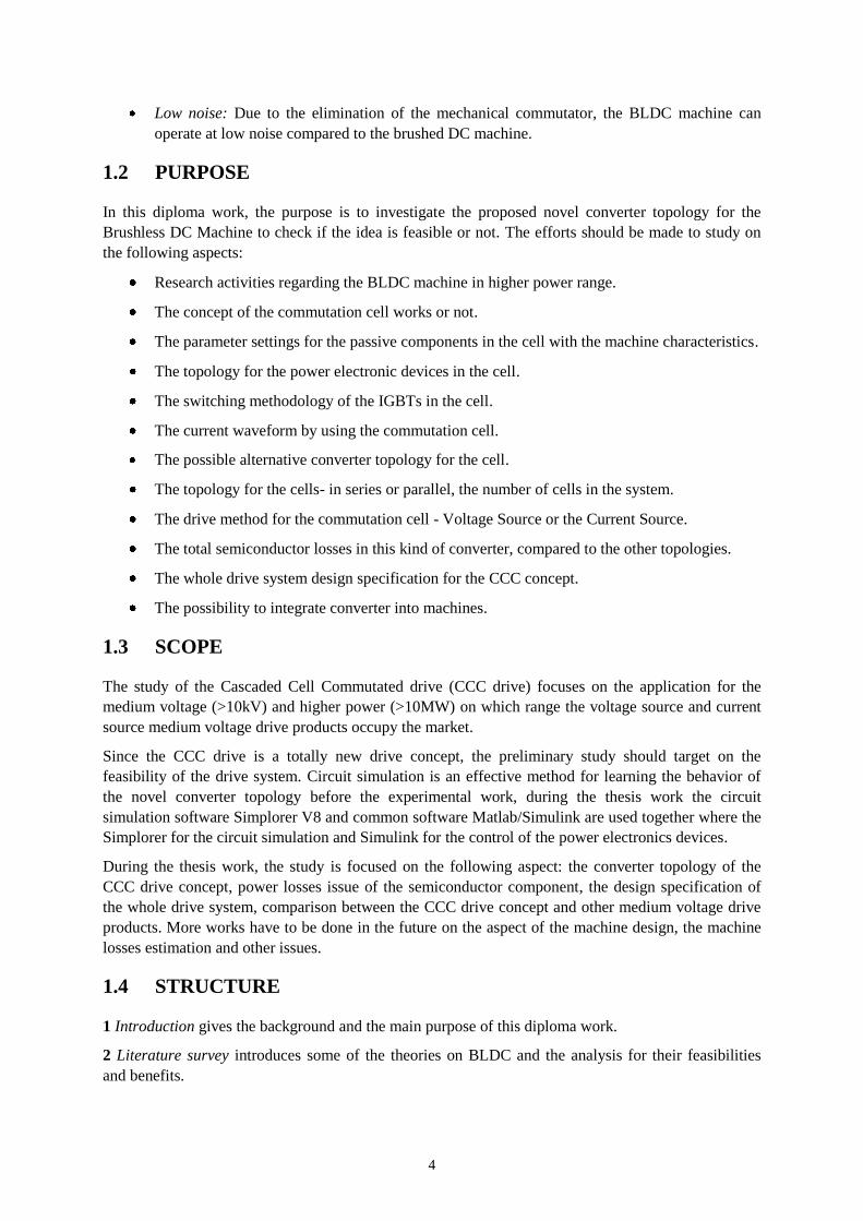
Cycloconverters (CCs): Based on the thyristor technology, designed for the low-speed, high
power applications. The topology is shown in Figure 1-4.
(a) (b)
Figure 1-1 Delta-connected VSI topology: (a) 3L-NPC topology; (b) 4L-FC topology. [1]
2
(a) (b)
Figure 1-2 Star-connected VSI topology: (a) 2-level series connected H-bridge (SC-HB) topology; (b) 3-level
SC-HB topology. [1]
Figure 1-3 Current source LCI converter. [1]
3
Figure 1-4 Cycloconverter topology. [1]
In sum, various topologies of AC dives are available and occupy the medium voltage drive market,
while the utilization of the dc machine is limited to a narrow application range and has little market
share.
Though AC drives are popular, some comparisons here are made to study the merits of the DC drive
concept.
Main advantage for traditional DC machine over AC machine:
Easy and accurate speed control with dc drives: The speed of the DC machine can be changed
very easily by adjusting the armature voltage of the machine and the field weakening, while
the speed control in AC machine is much more complex.
Constant torque from zero to base speed: The torque of the DC machine is proportional to the
machine armature current and the flux, which means that with the constant armature current
from zero to base speed, the torque can be kept constant independent of the speed change by
adjusting the armature voltage.
Wide speed range with constant power: When the speed is adjusted in the field weakening
range, the flux is decreased by reducing the magnetizing current and the maximum speed of
the DC machine can be reached to a high value. The armature voltage and current keep
constant so the constant power can be obtained.
Higher power density: Due to the nearly square wave current and trapezoidal back-emf
voltage in the DC machine, the power density for the DC machine is much higher than the
sinusoidal wave AC drive.
Secondly, there are some advantages for BLDC (Brushless DC) machine over traditional DC machine:
No mechanical brushes, easy for the maintenance: Due to the utilization of the electronic
commutator, the BLDC machine does not have the problem for brush maintenance.
4
Low noise: Due to the elimination of the mechanical commutator, the BLDC machine can
operate at low noise compared to the brushed DC machine.
1.2 PURPOSE
In this diploma work, the purpose is to investigate the proposed novel converter topology for the
Brushless DC Machine to check if the idea is feasible or not. The efforts should be made to study on
the following aspects:
Research activities regarding the BLDC machine in higher power range.
The concept of the commutation cell works or not.
The parameter settings for the passive components in the cell with the machine characteristics.
The topology for the power electronic devices in the cell.
The switching methodology of the IGBTs in the cell.
The current waveform by using the commutation cell.
The possible alternative converter topology for the cell.
The topology for the cells- in series or parallel, the number of cells in the system.
The drive method for the commutation cell - Voltage Source or the Current Source.
The total semiconductor losses in this kind of converter, compared to the other topologies.
The whole drive system design specification for the CCC concept.
The possibility to integrate converter into machines.
1.3 SCOPE
The study of the Cascaded Cell Commutated drive (CCC drive) focuses on the application for the
medium voltage (>10kV) and higher power (>10MW) on which range the voltage source and current
source medium voltage drive products occupy the market.
Since the CCC drive is a totally new drive concept, the preliminary study should target on the
feasibility of the drive system. Circuit simulation is an effective method for learning the behavior of
the novel converter topology before the experimental work, during the thesis work the circuit
simulation software Simplorer V8 and common software Matlab/Simulink are used together where the
Simplorer for the circuit simulation and Simulink for the control of the power electronics devices.
During the thesis work, the study is focused on the following aspect: the converter topology of the
CCC drive concept, power losses issue of the semiconductor component, the design specification of
the whole drive system, comparison between the CCC drive concept and other medium voltage drive
products. More works have to be done in the future on the aspect of the machine design, the machine
losses estimation and other issues.
1.4 STRUCTURE
1 Introduction gives the background and the main purpose of this diploma work.
2 Literature survey introduces some of the theories on BLDC and the analysis for their feasibilities
and benefits.

5
3 Proposed converter topology contains the introductions to the simulation software during the thesis
work, the description of the commutation cell.
4 Simulation results and analysis gives the results obtained by the simulation work.
5 Power losses in CCC converter analyze the power losses in the CCC converter.
6 System design specification describes the whole system design and the converter-machine
integration issue.
7 Conclusions and future work contains the conclusion of the diploma work and the future work on
this topic.
Appendix A Contains the simulation interface of the software.
Appendix B Contains the calculation results for the power losses in the converter.
Appendix C Contains the data sheet of the selected components.
6
2 LITERATURE SURVEY
2.1 TRADITIONAL BLDC TOPOLOGY
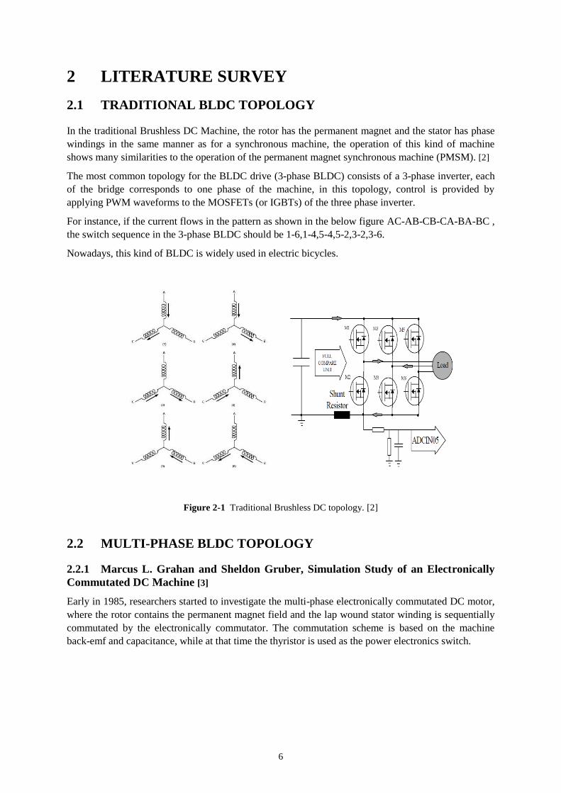
In the traditional Brushless DC Machine, the rotor has the permanent magnet and the stator has phase
windings in the same manner as for a synchronous machine, the operation of this kind of machine
shows many similarities to the operation of the permanent magnet synchronous machine (PMSM). [2]
The most common topology for the BLDC drive (3-phase BLDC) consists of a 3-phase inverter, each
of the bridge corresponds to one phase of the machine, in this topology, control is provided by
applying PWM waveforms to the MOSFETs (or IGBTs) of the three phase inverter.
For instance, if the current flows in the pattern as shown in the below figure AC-AB-CB-CA-BA-BC ,
the switch sequence in the 3-phase BLDC should be 1-6,1-4,5-4,5-2,3-2,3-6.
Nowadays, this kind of BLDC is widely used in electric bicycles.
Figure 2-1 Traditional Brushless DC topology. [2]
2.2 MULTI-PHASE BLDC TOPOLOGY
2.2.1 Marcus L. Grahan and Sheldon Gruber, Simulation Study of an Electronically
Commutated DC Machine [3]
Early in 1985, researchers started to investigate the multi-phase electronically commutated DC motor,
where the rotor contains the permanent magnet field and the lap wound stator winding is sequentially
commutated by the electronically commutator. The commutation scheme is based on the machine
back-emf and capacitance, while at that time the thyristor is used as the power electronics switch.
7
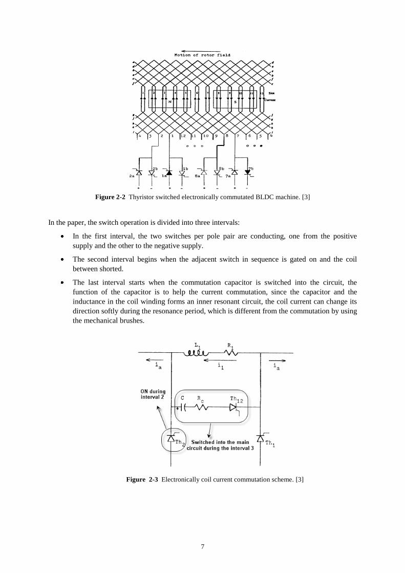
Figure 2-2 Thyristor switched electronically commutated BLDC machine. [3]
In the paper, the switch operation is divided into three intervals:
In the first interval, the two switches per pole pair are conducting, one from the positive
supply and the other to the negative supply.
The second interval begins when the adjacent switch in sequence is gated on and the coil
between shorted.
The last interval starts when the commutation capacitor is switched into the circuit, the
function of the capacitor is to help the current commutation, since the capacitor and the
inductance in the coil winding forms an inner resonant circuit, the coil current can change its
direction softly during the resonance period, which is different from the commutation by using
the mechanical brushes.
Figure 2-3 Electronically coil current commutation scheme. [3]
8
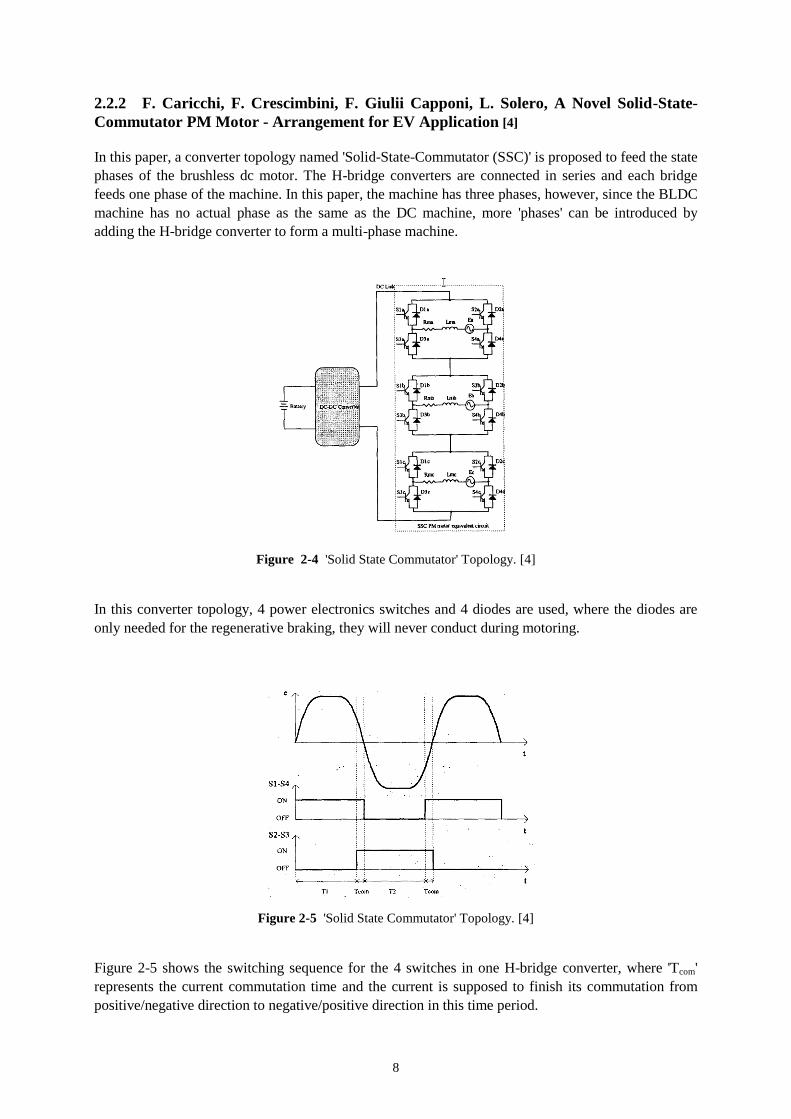
2.2.2 F. Caricchi, F. Crescimbini, F. Giulii Capponi, L. Solero, A Novel Solid-State-
Commutator PM Motor - Arrangement for EV Application [4]
In this paper, a converter topology named 'Solid-State-Commutator (SSC)' is proposed to feed the state
phases of the brushless dc motor. The H-bridge converters are connected in series and each bridge
feeds one phase of the machine. In this paper, the machine has three phases, however, since the BLDC
machine has no actual phase as the same as the DC machine, more 'phases' can be introduced by
adding the H-bridge converter to form a multi-phase machine.
Figure 2-4 'Solid State Commutator' Topology. [4]
In this converter topology, 4 power electronics switches and 4 diodes are used, where the diodes are
only needed for the regenerative braking, they will never conduct during motoring.
Figure 2-5 'Solid State Commutator' Topology. [4]
Figure 2-5 shows the switching sequence for the 4 switches in one H-bridge converter, where 'Tcom'
represents the current commutation time and the current is supposed to finish its commutation from
positive/negative direction to negative/positive direction in this time period.
9
In one period the control signal for switch 1 and 4 are on from the beginning instant of T1 to the next
positive back-emf zero-crossing time, while the switch 2 and 3 are on from the beginning of the
commutation time (Tcom) to the next negative back-emf zero-crossing time. During the rest of the time,
the control signal is off and vice-versa.
In the paper, it is pointed out that the coil current will commutate successfully from positive/negative
to negative/positive before the positive/negative emf zero-crossing time by using the above switching
strategy.
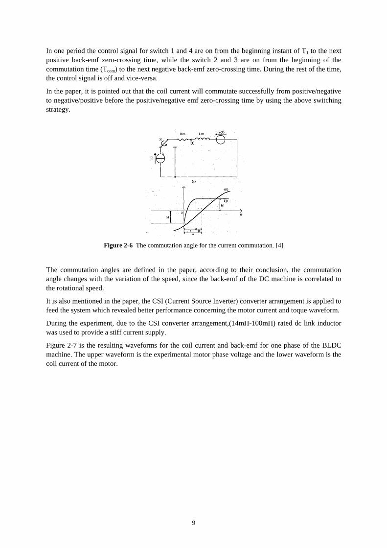
Figure 2-6 The commutation angle for the current commutation. [4]
The commutation angles are defined in the paper, according to their conclusion, the commutation
angle changes with the variation of the speed, since the back-emf of the DC machine is correlated to
the rotational speed.
It is also mentioned in the paper, the CSI (Current Source Inverter) converter arrangement is applied to
feed the system which revealed better performance concerning the motor current and toque waveform.
During the experiment, due to the CSI converter arrangement,(14mH-100mH) rated dc link inductor
was used to provide a stiff current supply.
Figure 2-7 is the resulting waveforms for the coil current and back-emf for one phase of the BLDC
machine. The upper waveform is the experimental motor phase voltage and the lower waveform is the
coil current of the motor.
10
Figure 2-7 Back-emf and coil current waveform by using the 100mH input filter. [4]
2.2.3 DDS PAPER - SPACE-SHIFT, SPLIT-PHASE HIGH SPEED MOTOR [5]
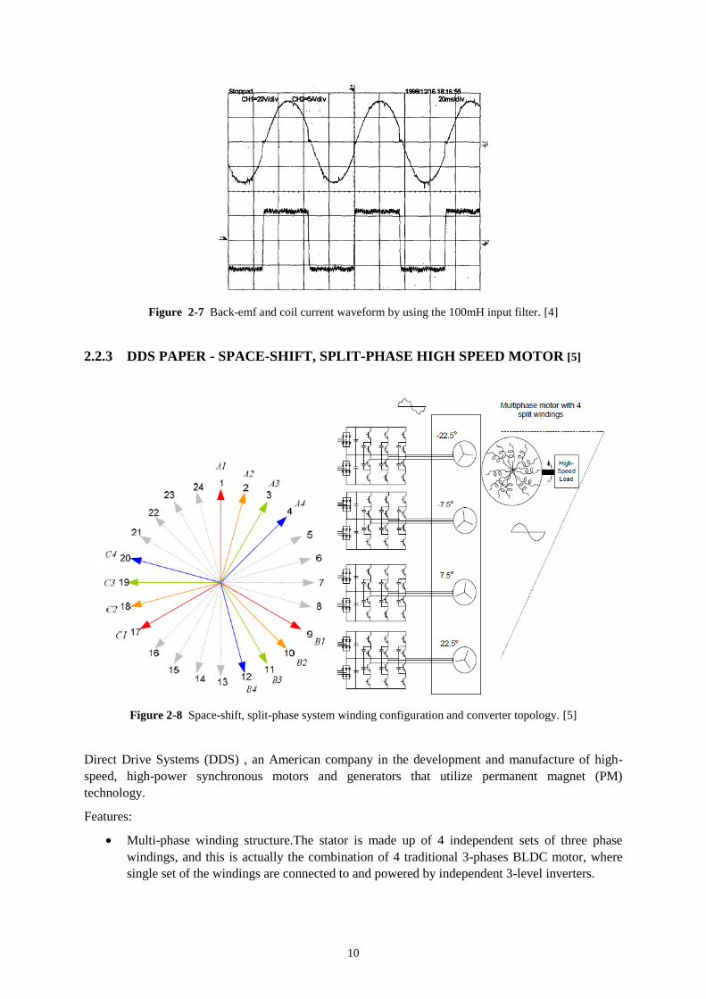
Figure 2-8 Space-shift, split-phase system winding configuration and converter topology. [5]
Direct Drive Systems (DDS) , an American company in the development and manufacture of high-
speed, high-power synchronous motors and generators that utilize permanent magnet (PM)
technology.
Features:
Multi-phase winding structure.The stator is made up of 4 independent sets of three phase
windings, and this is actually the combination of 4 traditional 3-phases BLDC motor, where
single set of the windings are connected to and powered by independent 3-level inverters.
11
Due to the introduction of this kind of winding structure, there is a phase shift between each
two phases, for instance, between A1 and A2, the phase A in the first and second 3-phase
winding sets respectively and the phase shift is dependent on the number of the independent
sets of three phase windings. In this case, there are 4 sets of three phase windings: (A1, B1,
C1), (A2, B2, C2), (A3, B3, C3), (A4, B4, C4), thus the phase shift is 180/4/3=15°
What's more, the proposed winding configuration allows the harmonic current cancellation by
using this space-shift, split-phase concept and this converter topology with this motor design
reduces the switching frequency and has a better modularity.
2.2.4 CONVERTEAM PATENT - FULL ELECTRONICALLY COMMUTATED
MACHINE [6]
CONVERTEAM, a French company, has developed a 15MW BLDC by using the novel electronically
commutated circuit inside the machine, which is named as „Active Stator Technology '.
By using this technique, the motor and the associated power electronics commutator have been
integrated together as a system.
In each switching stage, the power electronic devices RB (Reverse Blocked) -GTO has been used in
the circuit, the first RB-GTO is capable of being turned on and off by gate control having its anode
connected to the first dc terminal, while the second RB-GTO is capable of being turned on and off by
gate control have its cathode connected to the second dc terminal.
The thyristor pairs in this circuit are commutated under the help of back-emf.
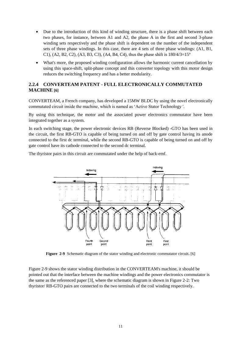
Figure 2-9 Schematic diagram of the stator winding and electronic commutator circuit. [6]
Figure 2-9 shows the stator winding distribution in the CONVERTEAM's machine, it should be
pointed out that the interface between the machine windings and the power electronics commutator is
the same as the referenced paper [3], where the schematic diagram is shown in Figure 2-2: Two
thyristor/ RB-GTO pairs are connected to the two terminals of the coil winding respectively.
12
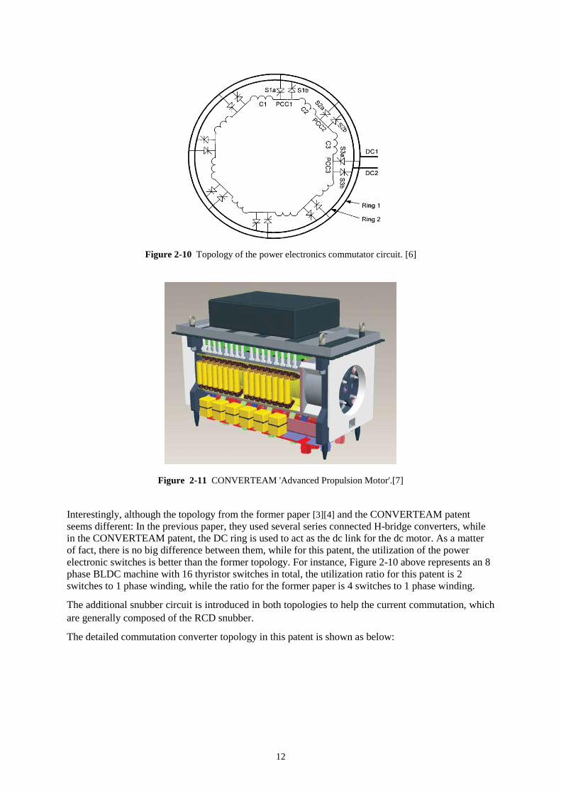
Figure 2-10 Topology of the power electronics commutator circuit. [6]
Figure 2-11 CONVERTEAM 'Advanced Propulsion Motor'.[7]
Interestingly, although the topology from the former paper [3][4] and the CONVERTEAM patent
seems different: In the previous paper, they used several series connected H-bridge converters, while
in the CONVERTEAM patent, the DC ring is used to act as the dc link for the dc motor. As a matter
of fact, there is no big difference between them, while for this patent, the utilization of the power
electronic switches is better than the former topology. For instance, Figure 2-10 above represents an 8
phase BLDC machine with 16 thyristor switches in total, the utilization ratio for this patent is 2
switches to 1 phase winding, while the ratio for the former paper is 4 switches to 1 phase winding.
The additional snubber circuit is introduced in both topologies to help the current commutation, which
are generally composed of the RCD snubber.
The detailed commutation converter topology in this patent is shown as below:
13
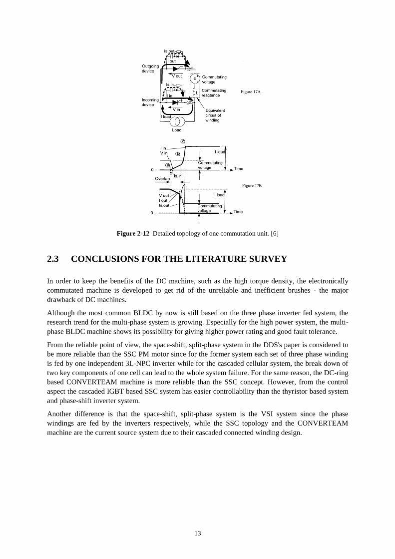
Figure 2-12 Detailed topology of one commutation unit. [6]
2.3 CONCLUSIONS FOR THE LITERATURE SURVEY
In order to keep the benefits of the DC machine, such as the high torque density, the electronically
commutated machine is developed to get rid of the unreliable and inefficient brushes - the major
drawback of DC machines.
Although the most common BLDC by now is still based on the three phase inverter fed system, the
research trend for the multi-phase system is growing. Especially for the high power system, the multi-
phase BLDC machine shows its possibility for giving higher power rating and good fault tolerance.
From the reliable point of view, the space-shift, split-phase system in the DDS's paper is considered to
be more reliable than the SSC PM motor since for the former system each set of three phase winding
is fed by one independent 3L-NPC inverter while for the cascaded cellular system, the break down of
two key components of one cell can lead to the whole system failure. For the same reason, the DC-ring
based CONVERTEAM machine is more reliable than the SSC concept. However, from the control
aspect the cascaded IGBT based SSC system has easier controllability than the thyristor based system
and phase-shift inverter system.
Another difference is that the space-shift, split-phase system is the VSI system since the phase
windings are fed by the inverters respectively, while the SSC topology and the CONVERTEAM
machine are the current source system due to their cascaded connected winding design.
14
3 PROPOSED CONVERTER TOPOLOGY
3.1 SIMULATION SOFTWARE
3.1.1 SIMPLORER
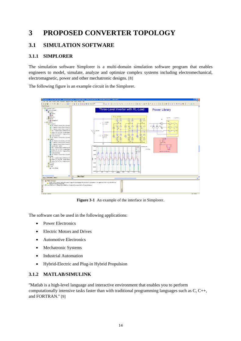
The simulation software Simplorer is a multi-domain simulation software program that enables
engineers to model, simulate, analyze and optimize complex systems including electromechanical,
electromagnetic, power and other mechatronic designs. [8]
The following figure is an example circuit in the Simplorer.
Figure 3-1 An example of the interface in Simplorer.
The software can be used in the following applications:
Power Electronics
Electric Motors and Drives
Automotive Electronics
Mechatronic Systems
Industrial Automation
Hybrid-Electric and Plug-in Hybrid Propulsion
3.1.2 MATLAB/SIMULINK
''Matlab is a high-level language and interactive environment that enables you to perform
computationally intensive tasks faster than with traditional programming languages such as C, C++,
and FORTRAN.'' [9]
15
''Simulink is an environment for multinomial simulation and Model-Based Design for dynamic and
embedded systems. It provides an interactive graphical environment and a customizable set of block
libraries that let you design , simulate, implement , and test a variety of time-varying systems,
including communications, controls ,signal processing, video processing, and image processing. '' [10]
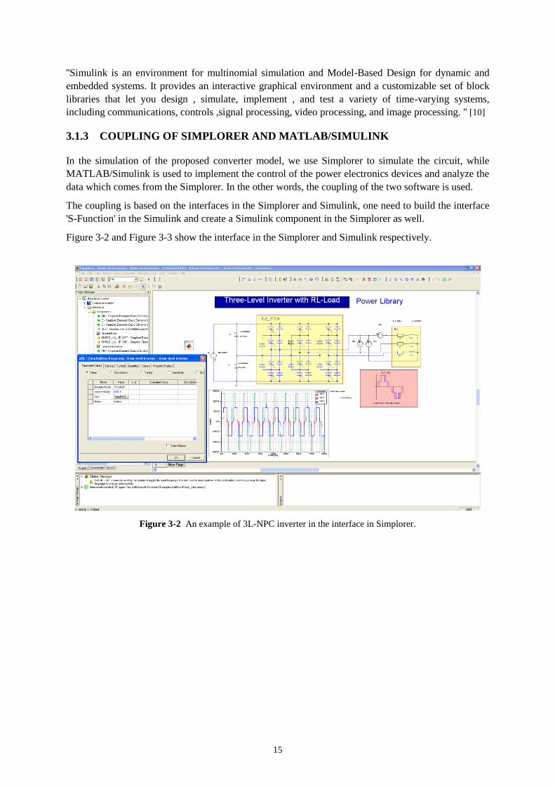
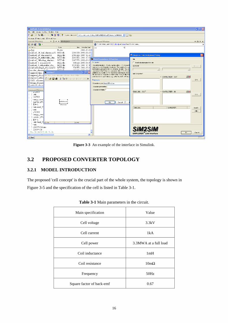
3.1.3 COUPLING OF SIMPLORER AND MATLAB/SIMULINK
In the simulation of the proposed converter model, we use Simplorer to simulate the circuit, while
MATLAB/Simulink is used to implement the control of the power electronics devices and analyze the
data which comes from the Simplorer. In the other words, the coupling of the two software is used.
The coupling is based on the interfaces in the Simplorer and Simulink, one need to build the interface
'S-Function' in the Simulink and create a Simulink component in the Simplorer as well.
Figure 3-2 and Figure 3-3 show the interface in the Simplorer and Simulink respectively.
Figure 3-2 An example of 3L-NPC inverter in the interface in Simplorer.
16
Figure 3-3 An example of the interface in Simulink.
3.2 PROPOSED CONVERTER TOPOLOGY
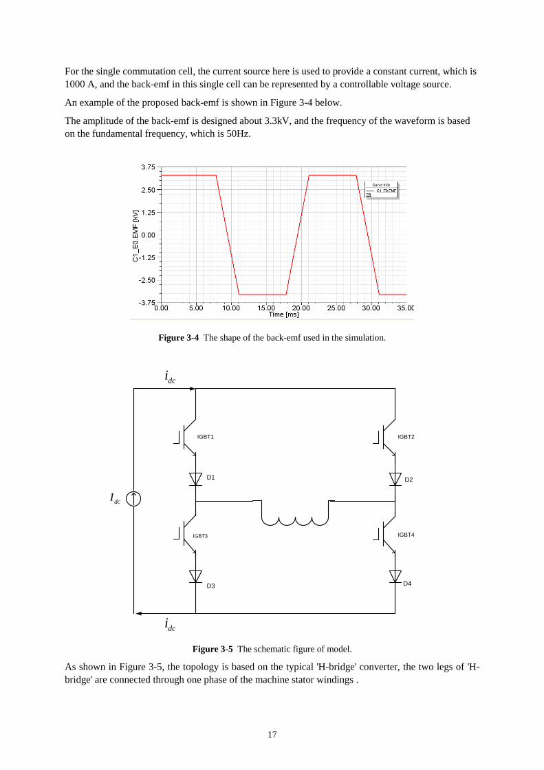
3.2.1 MODEL INTRODUCTION
The proposed 'cell concept' is the crucial part of the whole system, the topology is shown in
Figure 3-5 and the specification of the cell is listed in Table 3-1.
Table 3-1 Main parameters in the circuit.
Main specification Value
Cell voltage 3.3kV
Cell current 1kA
Cell power 3.3MWA at a full load
Coil inductance 1mH
Coil resistance 10mΩ
Frequency 50Hz
Square factor of back-emf 0.67
17
For the single commutation cell, the current source here is used to provide a constant current, which is
1000 A, and the back-emf in this single cell can be represented by a controllable voltage source.
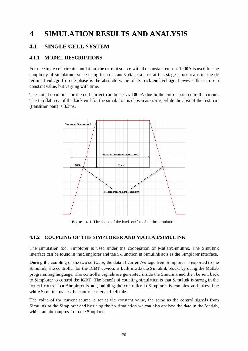
An example of the proposed back-emf is shown in Figure 3-4 below.
The amplitude of the back-emf is designed about 3.3kV, and the frequency of the waveform is based
on the fundamental frequency, which is 50Hz.
Figure 3-4 The shape of the back-emf used in the simulation.
dcI
dci
dci
IGBT1 IGBT2
IGBT3 IGBT4
D1 D2
D3 D4
Figure 3-5 The schematic figure of model.
As shown in Figure 3-5, the topology is based on the typical 'H-bridge' converter, the two legs of 'H-
bridge' are connected through one phase of the machine stator windings .
18
In the 'H-bridge', one single power electronic switch in the circuit is the combination of IGBT and
diode. On each leg of the converter, (4 legs in total) one IGBT is connected in series with one diode to
achieve to be fully controllable and bidirectional voltage blocking. The function of the diode is to
make sure that the machine current flows only in one direction when the converter is operating at the
motor mode.
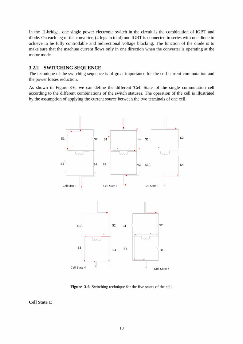
3.2.2 SWITCHING SEQUENCE
The technique of the switching sequence is of great importance for the coil current commutation and
the power losses reduction.
As shown in Figure 3-6, we can define the different 'Cell State' of the single commutation cell
according to the different combinations of the switch statuses. The operation of the cell is illustrated
by the assumption of applying the current source between the two terminals of one cell.
+ -+ -
+- +-
Cell State 2 Cell State 1
Cell State 5 Cell State 4
S1
S4S3
S2 S1 S2
S3 S4
S1 S2
S3S4
S1 S2
S3S4
+ -
Cell State 3
S1S2
S3 S4
Figure 3-6 Switching technique for the five states of the cell.
Cell State 1:
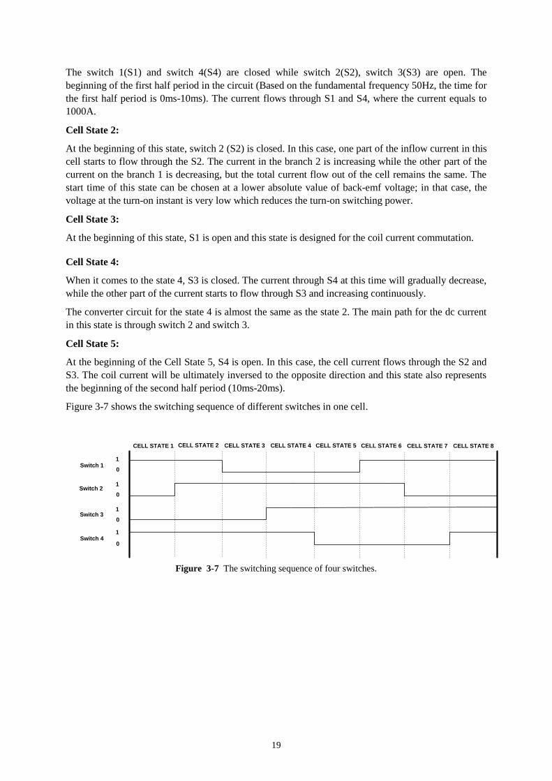
19
The switch 1(S1) and switch 4(S4) are closed while switch 2(S2), switch 3(S3) are open. The
beginning of the first half period in the circuit (Based on the fundamental frequency 50Hz, the time for
the first half period is 0ms-10ms). The current flows through S1 and S4, where the current equals to
1000A.
Cell State 2:
At the beginning of this state, switch 2 (S2) is closed. In this case, one part of the inflow current in this
cell starts to flow through the S2. The current in the branch 2 is increasing while the other part of the
current on the branch 1 is decreasing, but the total current flow out of the cell remains the same. The
start time of this state can be chosen at a lower absolute value of back-emf voltage; in that case, the
voltage at the turn-on instant is very low which reduces the turn-on switching power.
Cell State 3:
At the beginning of this state, S1 is open and this state is designed for the coil current commutation.
Cell State 4:
When it comes to the state 4, S3 is closed. The current through S4 at this time will gradually decrease,
while the other part of the current starts to flow through S3 and increasing continuously.
The converter circuit for the state 4 is almost the same as the state 2. The main path for the dc current
in this state is through switch 2 and switch 3.
Cell State 5:
At the beginning of the Cell State 5, S4 is open. In this case, the cell current flows through the S2 and
S3. The coil current will be ultimately inversed to the opposite direction and this state also represents
the beginning of the second half period (10ms-20ms).
Figure 3-7 shows the switching sequence of different switches in one cell.
CELL STATE 1 CELL STATE 2 CELL STATE 3 CELL STATE 4 CELL STATE 6 CELL STATE 7CELL STATE 5 CELL STATE 8
Switch 1
Switch 2
Switch 3
Switch 4
1
0
1
1
1
0
0
0
Figure 3-7 The switching sequence of four switches.
20
4 SIMULATION RESULTS AND ANALYSIS
4.1 SINGLE CELL SYSTEM
4.1.1 MODEL DESCRIPTIONS
For the single cell circuit simulation, the current source with the constant current 1000A is used for the
simplicity of simulation, since using the constant voltage source at this stage is not realistic: the dc
terminal voltage for one phase is the absolute value of its back-emf voltage, however this is not a
constant value, but varying with time.
The initial condition for the coil current can be set as 1000A due to the current source in the circuit.
The top flat area of the back-emf for the simulation is chosen as 6.7ms, while the area of the rest part
(transition part) is 3.3ms.
Figure 4-1 The shape of the back-emf used in the simulation.
4.1.2 COUPLING OF THE SIMPLORER AND MATLAB/SIMULINK
The simulation tool Simplorer is used under the cooperation of Matlab/Simulink. The Simulink
interface can be found in the Simplorer and the S-Function in Simulink acts as the Simplorer interface.
During the coupling of the two software, the data of current/voltage from Simplorer is exported to the
Simulink; the controller for the IGBT devices is built inside the Simulink block, by using the Matlab
programming language. The controller signals are generated inside the Simulink and then be sent back
to Simplorer to control the IGBT. The benefit of coupling simulation is that Simulink is strong in the
logical control but Simplorer is not, building the controller in Simplorer is complex and takes time
while Simulink makes the control easier and reliable.
The value of the current source is set as the constant value, the same as the control signals from
Simulink to the Simplorer and by using the co-simulation we can also analyze the data in the Matlab,
which are the outputs from the Simplorer.
21
4.1.3 SIMULATION RESULTS
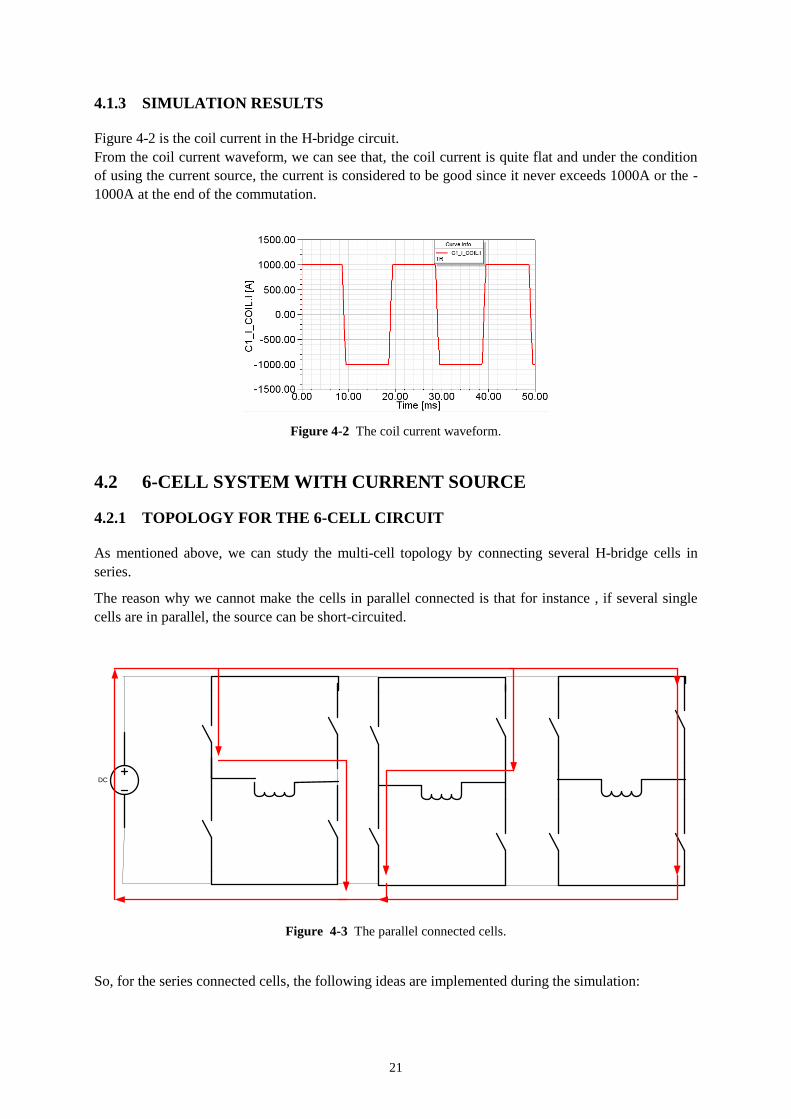
Figure 4-2 is the coil current in the H-bridge circuit.
From the coil current waveform, we can see that, the coil current is quite flat and under the condition
of using the current source, the current is considered to be good since it never exceeds 1000A or the -
1000A at the end of the commutation.
Figure 4-2 The coil current waveform.
4.2 6-CELL SYSTEM WITH CURRENT SOURCE
4.2.1 TOPOLOGY FOR THE 6-CELL CIRCUIT
As mentioned above, we can study the multi-cell topology by connecting several H-bridge cells in
series.
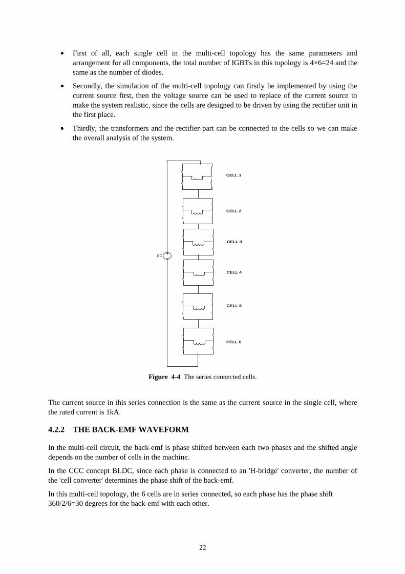
The reason why we cannot make the cells in parallel connected is that for instance , if several single
cells are in parallel, the source can be short-circuited.
DC
Figure 4-3 The parallel connected cells.
So, for the series connected cells, the following ideas are implemented during the simulation:
22
First of all, each single cell in the multi-cell topology has the same parameters and
arrangement for all components, the total number of IGBTs in this topology is 4×6=24 and the
same as the number of diodes.
Secondly, the simulation of the multi-cell topology can firstly be implemented by using the
current source first, then the voltage source can be used to replace of the current source to
make the system realistic, since the cells are designed to be driven by using the rectifier unit in
the first place.
Thirdly, the transformers and the rectifier part can be connected to the cells so we can make
the overall analysis of the system.
DC
CELL 1
CELL 2
CELL 3
CELL 4
CELL 5
CELL 6
Figure 4-4 The series connected cells.
The current source in this series connection is the same as the current source in the single cell, where
the rated current is 1kA.
4.2.2 THE BACK-EMF WAVEFORM
In the multi-cell circuit, the back-emf is phase shifted between each two phases and the shifted angle
depends on the number of cells in the machine.
In the CCC concept BLDC, since each phase is connected to an 'H-bridge' converter, the number of
the 'cell converter' determines the phase shift of the back-emf.
In this multi-cell topology, the 6 cells are in series connected, so each phase has the phase shift
360/2/6=30 degrees for the back-emf with each other.
23
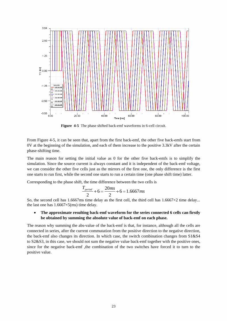
Figure 4-5 The phase shifted back-emf waveforms in 6-cell circuit.
From Figure 4-5, it can be seen that, apart from the first back-emf, the other five back-emfs start from
0V at the beginning of the simulation, and each of them increase to the positive 3.3kV after the certain
phase-shifting time.
The main reason for setting the initial value as 0 for the other five back-emfs is to simplify the
simulation. Since the source current is always constant and it is independent of the back-emf voltage,
we can consider the other five cells just as the mirrors of the first one, the only difference is the first
one starts to run first, while the second one starts to run a certain time (one phase shift time) latter.
Corresponding to the phase shift, the time difference between the two cells is
206 6 1.6667
2 2
periodT msms
So, the second cell has 1.6667ms time delay as the first cell, the third cell has 1.6667×2 time delay...
the last one has 1.6667×5(ms) time delay.
The approximate resulting back-emf waveform for the series connected 6 cells can firstly
be obtained by summing the absolute value of back-emf on each phase.
The reason why summing the abs-value of the back-emf is that, for instance, although all the cells are
connected in series, after the current commutation from the positive direction to the negative direction,
the back-emf also changes its direction. In which case, the switch combination changes from S1&S4
to S2&S3, in this case, we should not sum the negative value back-emf together with the positive ones,
since for the negative back-emf ,the combination of the two switches have forced it to turn to the
positive value.
24
DC
N CELLS
N CELLS
+ -
+-
+ -
A
H
Z
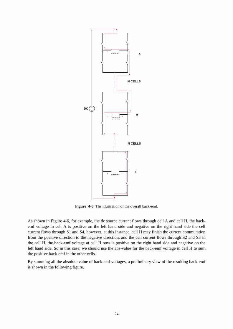
Figure 4-6 The illustration of the overall back-emf.
As shown in Figure 4-6, for example, the dc source current flows through cell A and cell H, the back-
emf voltage in cell A is positive on the left hand side and negative on the right hand side the cell
current flows through S1 and S4, however, at this instance, cell H may finish the current commutation
from the positive direction to the negative direction, and the cell current flows through S2 and S3 in
the cell H, the back-emf voltage at cell H now is positive on the right hand side and negative on the
left hand side. So in this case, we should use the abs-value for the back-emf voltage in cell H to sum
the positive back-emf in the other cells.
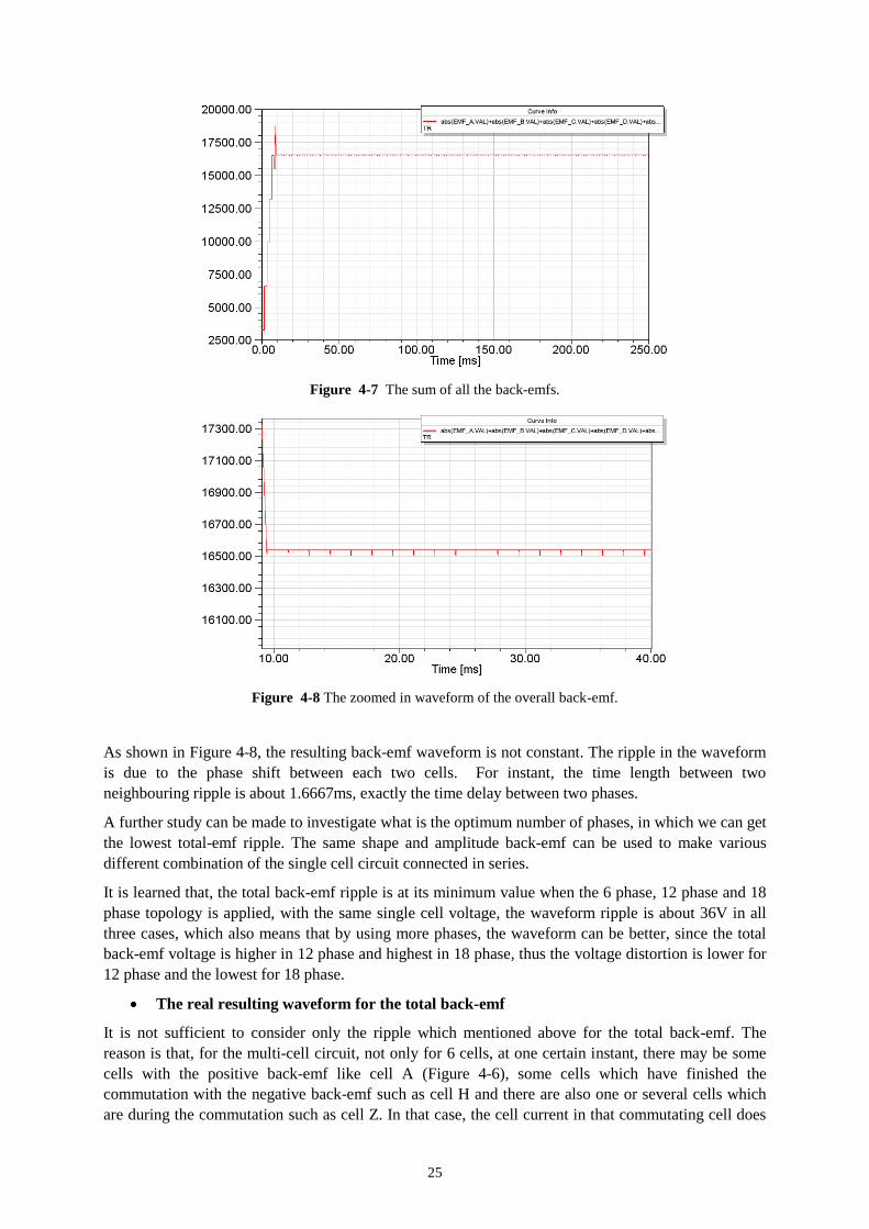
By summing all the absolute value of back-emf voltages, a preliminary view of the resulting back-emf
is shown in the following figure.
25
Figure 4-7 The sum of all the back-emfs.
Figure 4-8 The zoomed in waveform of the overall back-emf.
As shown in Figure 4-8, the resulting back-emf waveform is not constant. The ripple in the waveform
is due to the phase shift between each two cells. For instant, the time length between two
neighbouring ripple is about 1.6667ms, exactly the time delay between two phases.
A further study can be made to investigate what is the optimum number of phases, in which we can get
the lowest total-emf ripple. The same shape and amplitude back-emf can be used to make various
different combination of the single cell circuit connected in series.
It is learned that, the total back-emf ripple is at its minimum value when the 6 phase, 12 phase and 18
phase topology is applied, with the same single cell voltage, the waveform ripple is about 36V in all
three cases, which also means that by using more phases, the waveform can be better, since the total
back-emf voltage is higher in 12 phase and highest in 18 phase, thus the voltage distortion is lower for
12 phase and the lowest for 18 phase.
The real resulting waveform for the total back-emf
It is not sufficient to consider only the ripple which mentioned above for the total back-emf. The
reason is that, for the multi-cell circuit, not only for 6 cells, at one certain instant, there may be some
cells with the positive back-emf like cell A (Figure 4-6), some cells which have finished the
commutation with the negative back-emf such as cell H and there are also one or several cells which
are during the commutation such as cell Z. In that case, the cell current in that commutating cell does
26
not flow through the coils but through the switches only. For instance, in Figure 4-6 the path for the
cell current is through the S2 and S4 - during the commutation. In this case, the overall back-emf
decreases by the value of one cell's back-emf, the duration time for that phenomenon is the same as the
time for the commutation.
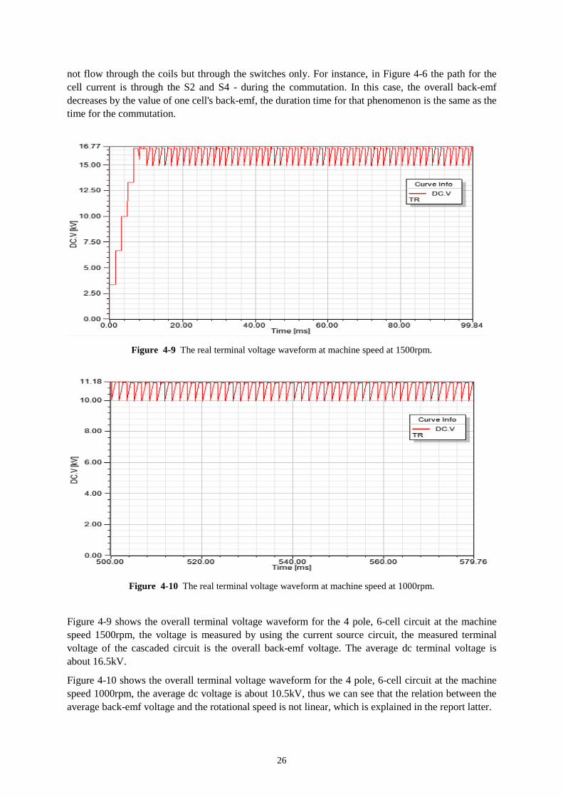
Figure 4-9 The real terminal voltage waveform at machine speed at 1500rpm.
Figure 4-10 The real terminal voltage waveform at machine speed at 1000rpm.
Figure 4-9 shows the overall terminal voltage waveform for the 4 pole, 6-cell circuit at the machine
speed 1500rpm, the voltage is measured by using the current source circuit, the measured terminal
voltage of the cascaded circuit is the overall back-emf voltage. The average dc terminal voltage is
about 16.5kV.
Figure 4-10 shows the overall terminal voltage waveform for the 4 pole, 6-cell circuit at the machine
speed 1000rpm, the average dc voltage is about 10.5kV, thus we can see that the relation between the
average back-emf voltage and the rotational speed is not linear, which is explained in the report latter.
27
Thus, the overall voltage waveform shown in Figure 4-9 and Figure 4-10 above is ruined by the
influence of this back-emf drop during the commutation state, the outcome of its influence by this
phenomenon is analyzed in the following part of report.
4.2.3 MODEL DESCRIPTIONS
As shown in Figure 4-4, 6 cells are in series connected, the current source with the constant current
1kA is connected to the cells.
The components in different cells are named uniformly; all of the components can be distinguished
clearly by adding their corresponding cell number in front of their names.
4.2.4 COULPING OF TWO SIMULATION SOFTWARE
For the multi-cell circuit, the interface and the controller in the Simulink is just the extended version of
the single cell circuit.
Here, each Matlab block controls the IGBTs in its corresponding cell and then the control signals are
sent back to Simplorer.
The input and output signals in the Simulink is about 6 times as the number in the single cell circuit.
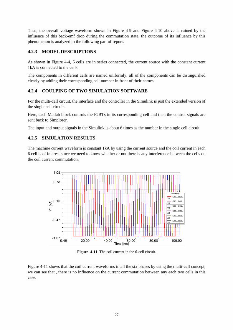
4.2.5 SIMULATION RESULTS
The machine current waveform is constant 1kA by using the current source and the coil current in each
6 cell is of interest since we need to know whether or not there is any interference between the cells on
the coil current commutation.
Figure 4-11 The coil current in the 6-cell circuit.
Figure 4-11 shows that the coil current waveforms in all the six phases by using the multi-cell concept,
we can see that , there is no influence on the current commutation between any each two cells in this
case.
28
4.3 6-CELL SYSTEM WITH VOLTAGE SOURCE
4.3.1 MODEL DESCRIPTIONS
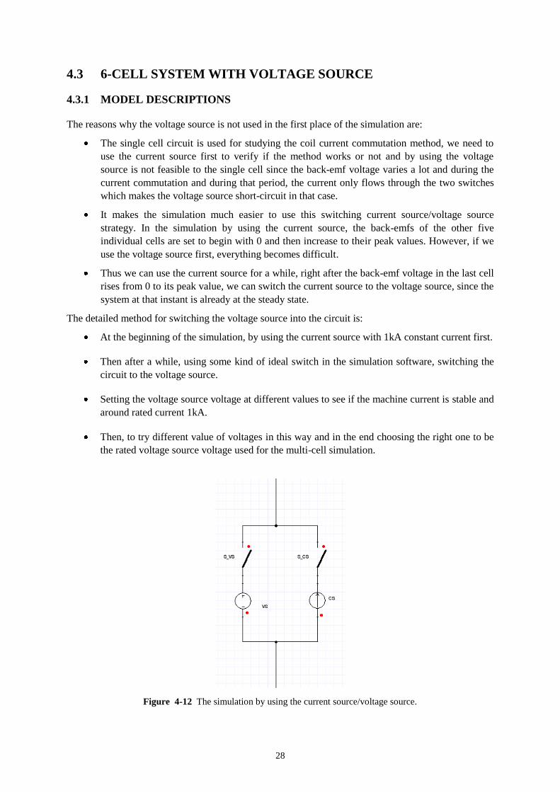
The reasons why the voltage source is not used in the first place of the simulation are:
The single cell circuit is used for studying the coil current commutation method, we need to
use the current source first to verify if the method works or not and by using the voltage
source is not feasible to the single cell since the back-emf voltage varies a lot and during the
current commutation and during that period, the current only flows through the two switches
which makes the voltage source short-circuit in that case.
It makes the simulation much easier to use this switching current source/voltage source
strategy. In the simulation by using the current source, the back-emfs of the other five
individual cells are set to begin with 0 and then increase to their peak values. However, if we
use the voltage source first, everything becomes difficult.
Thus we can use the current source for a while, right after the back-emf voltage in the last cell
rises from 0 to its peak value, we can switch the current source to the voltage source, since the
system at that instant is already at the steady state.
The detailed method for switching the voltage source into the circuit is:
At the beginning of the simulation, by using the current source with 1kA constant current first.
Then after a while, using some kind of ideal switch in the simulation software, switching the
circuit to the voltage source.
Setting the voltage source voltage at different values to see if the machine current is stable and
around rated current 1kA.
Then, to try different value of voltages in this way and in the end choosing the right one to be
the rated voltage source voltage used for the multi-cell simulation.
Figure 4-12 The simulation by using the current source/voltage source.
29
4.3.2 SIMULATION RESULTS
1) The result for the machine current
Figure 4-13 shows the machine current during the simulation time, the current source is used during
the first 50ms, from 50ms to the end of simulation time (800ms), the voltage source is switched in to
the circuit.
(a) (b)
Figure 4-13 The machine current by using current source/voltage source: (a) The machine current waveform in
800ms; (b) The zoom-in figure of the machine current before and after 50ms.
One problem should be pointed out is that: the value for the current source is set as 1kA at the first
50ms, however, after that instance, the current should be changed from 1kA to 0 in the control block
in the Simulink, otherwise, the current source would influence the current waveform, say, the
waveform would become better under the influence of the current source, this fools the observer in
some extent. Accordingly, the voltage value for the voltage source should be set as 0 during the first
50ms, and be changed to the rated value since 50ms to the end of the simulation time.
It can be seen from Figure 4-13 (b) that, at the first 50ms, the machine current is flat by using the
current source. From 50ms to 800ms, there are pulsations to the machine current waveform.
The pulsation on the machine current is due to the fact which mentioned before: the non-constant
nature of the resulting machine back-emf voltage. The overall back-emf voltage decreases by a certain
amount during the commutation state of each cell, this phenomenon causes the pulsation of the
machine waveform.
What should also be pointed out is that, for the traditional brushed dc machine fed by the voltage
controllable thyristor rectifier, due to the same non-constant phenomenal of the back-emf voltage, the
machine current is also not constant, normally the ratio of the peak-peak current ripple is within 30%
of the rated dc current by using the rectifier unit and in the specific case, the filter inductor can also be
added into the circuit to reduce the peak-peak current ripple based on the customer's demand.
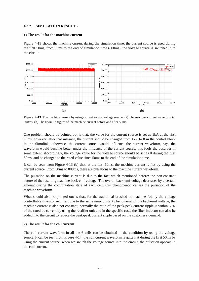
2) The result for the coil current
The coil current waveform in all the 6 cells can be obtained in the condition by using the voltage
source. It can be seen from Figure 4-14, the coil current waveform is quite flat during the first 50ms by
using the current source, when we switch the voltage source into the circuit; the pulsation appears in
the coil current.
30
Figure 4-14 The coil current by using current source/voltage source.
4.4 6-CELL SYSTEM WITH RECTIFIER
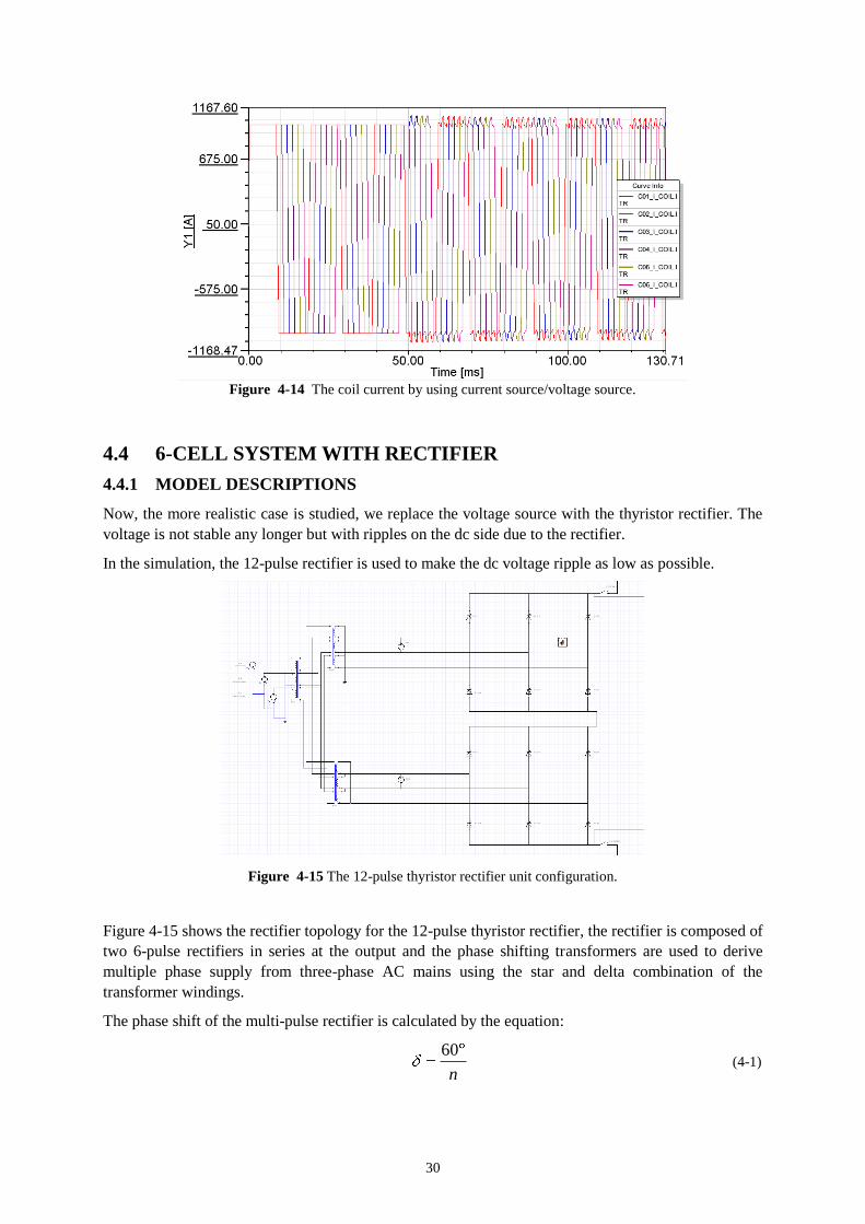
4.4.1 MODEL DESCRIPTIONS
Now, the more realistic case is studied, we replace the voltage source with the thyristor rectifier. The
voltage is not stable any longer but with ripples on the dc side due to the rectifier.
In the simulation, the 12-pulse rectifier is used to make the dc voltage ripple as low as possible.
Figure 4-15 The 12-pulse thyristor rectifier unit configuration.
Figure 4-15 shows the rectifier topology for the 12-pulse thyristor rectifier, the rectifier is composed of
two 6-pulse rectifiers in series at the output and the phase shifting transformers are used to derive
multiple phase supply from three-phase AC mains using the star and delta combination of the
transformer windings.
The phase shift of the multi-pulse rectifier is calculated by the equation:
60
n (4-1)
31
where n refers to the number of the 6-pulse rectifier and δ is the phase shift for the transformer
windings.
So, for the 12-pulse rectifier, the phase shift between the two transformer windings is 30 degree and
the star and delta connected windings are used. The transformer turns ratio between the primary
winding and star winding is 2 and the ratio between the primary winding and delta winding is 2/√3.
Due to the phase shift introduced by the transformer winding, the dc voltage ripple of the 12-pulse
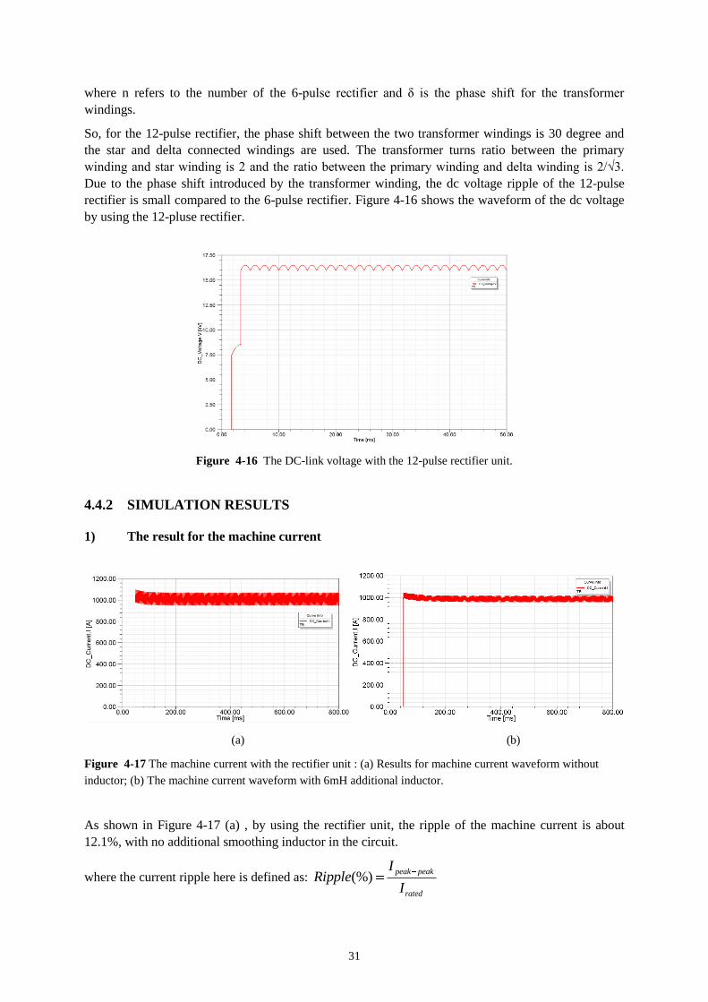
rectifier is small compared to the 6-pulse rectifier. Figure 4-16 shows the waveform of the dc voltage
by using the 12-pluse rectifier.
Figure 4-16 The DC-link voltage with the 12-pulse rectifier unit.
4.4.2 SIMULATION RESULTS
1) The result for the machine current
(a) (b)
Figure 4-17 The machine current with the rectifier unit : (a) Results for machine current waveform without
inductor; (b) The machine current waveform with 6mH additional inductor.
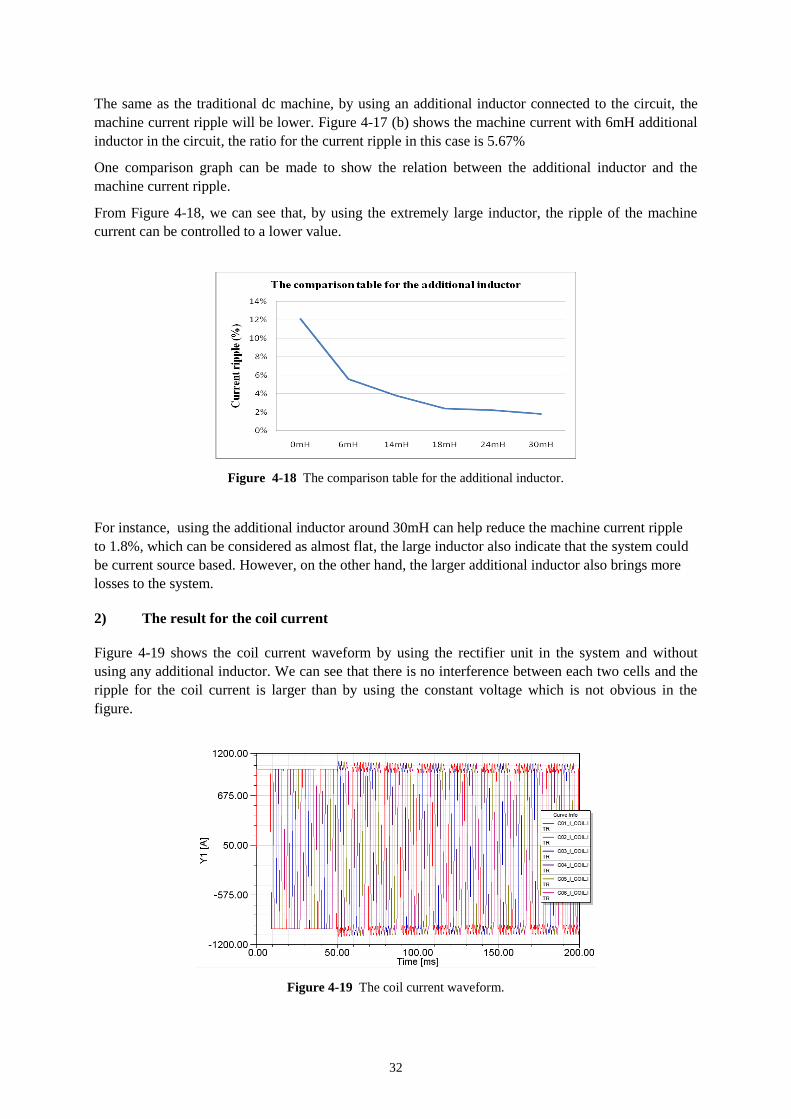
As shown in Figure 4-17 (a) , by using the rectifier unit, the ripple of the machine current is about
12.1%, with no additional smoothing inductor in the circuit.
where the current ripple here is defined as: (%)peak peak
rated
IRipple
I
32
The same as the traditional dc machine, by using an additional inductor connected to the circuit, the
machine current ripple will be lower. Figure 4-17 (b) shows the machine current with 6mH additional
inductor in the circuit, the ratio for the current ripple in this case is 5.67%
One comparison graph can be made to show the relation between the additional inductor and the
machine current ripple.
From Figure 4-18, we can see that, by using the extremely large inductor, the ripple of the machine
current can be controlled to a lower value.
Figure 4-18 The comparison table for the additional inductor.
For instance, using the additional inductor around 30mH can help reduce the machine current ripple
to 1.8%, which can be considered as almost flat, the large inductor also indicate that the system could
be current source based. However, on the other hand, the larger additional inductor also brings more
losses to the system.
2) The result for the coil current
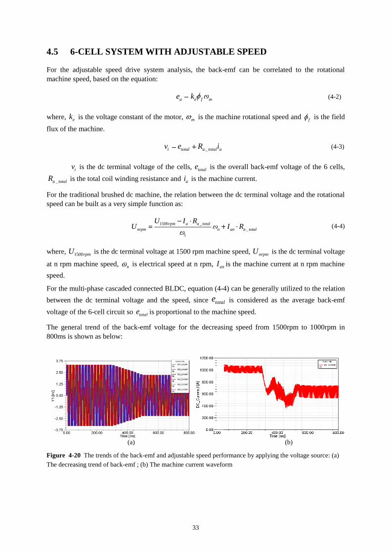
Figure 4-19 shows the coil current waveform by using the rectifier unit in the system and without
using any additional inductor. We can see that there is no interference between each two cells and the
ripple for the coil current is larger than by using the constant voltage which is not obvious in the
figure.
Figure 4-19 The coil current waveform.
33
4.5 6-CELL SYSTEM WITH ADJUSTABLE SPEED
For the adjustable speed drive system analysis, the back-emf can be correlated to the rotational
machine speed, based on the equation:
a e f me k (4-2)
where, ek is the voltage constant of the motor, m is the machine rotational speed and f is the field
flux of the machine.
_t total a total av e R i (4-3)
tv is the dc terminal voltage of the cells, totale is the overall back-emf voltage of the 6 cells,
_a totalR is the total coil winding resistance and ai is the machine current.
For the traditional brushed dc machine, the relation between the dc terminal voltage and the rotational
speed can be built as a very simple function as:
1500 _
_
1
rpm a a total
nrpm n an a total
U I RU I R (4-4)
where, 1500rpmU is the dc terminal voltage at 1500 rpm machine speed, nrpmU is the dc terminal voltage
at n rpm machine speed, n is electrical speed at n rpm, anI is the machine current at n rpm machine
speed.
For the multi-phase cascaded connected BLDC, equation (4-4) can be generally utilized to the relation
between the dc terminal voltage and the speed, since totale is considered as the average back-emf
voltage of the 6-cell circuit so totale is proportional to the machine speed.
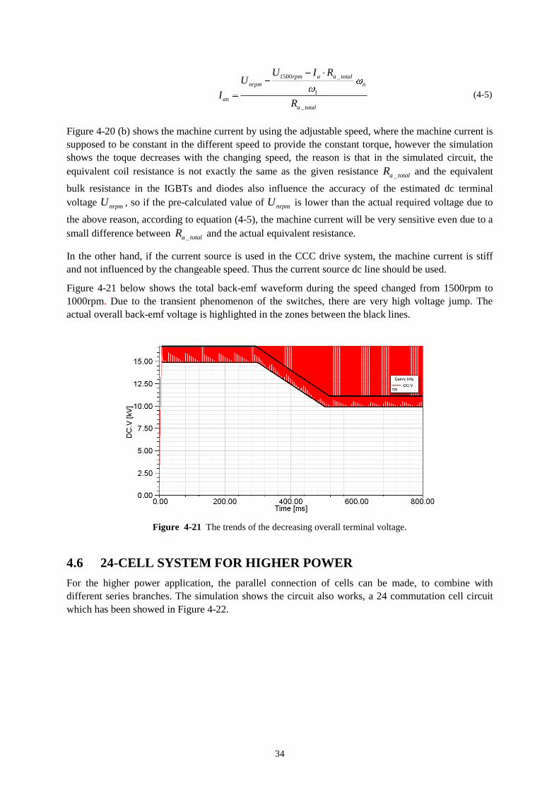
The general trend of the back-emf voltage for the decreasing speed from 1500rpm to 1000rpm in
800ms is shown as below:
(a) (b)
Figure 4-20 The trends of the back-emf and adjustable speed performance by applying the voltage source: (a)
The decreasing trend of back-emf ; (b) The machine current waveform
34
1500 _
1
_
rpm a a total
nrpm n
an
a total
U I RU
IR
(4-5)
Figure 4-20 (b) shows the machine current by using the adjustable speed, where the machine current is
supposed to be constant in the different speed to provide the constant torque, however the simulation
shows the toque decreases with the changing speed, the reason is that in the simulated circuit, the
equivalent coil resistance is not exactly the same as the given resistance _a totalR and the equivalent
bulk resistance in the IGBTs and diodes also influence the accuracy of the estimated dc terminal
voltage nrpmU , so if the pre-calculated value of nrpmU is lower than the actual required voltage due to
the above reason, according to equation (4-5), the machine current will be very sensitive even due to a
small difference between _a totalR and the actual equivalent resistance.
In the other hand, if the current source is used in the CCC drive system, the machine current is stiff
and not influenced by the changeable speed. Thus the current source dc line should be used.
Figure 4-21 below shows the total back-emf waveform during the speed changed from 1500rpm to
1000rpm. Due to the transient phenomenon of the switches, there are very high voltage jump. The
actual overall back-emf voltage is highlighted in the zones between the black lines.
Figure 4-21 The trends of the decreasing overall terminal voltage.
4.6 24-CELL SYSTEM FOR HIGHER POWER
For the higher power application, the parallel connection of cells can be made, to combine with
different series branches. The simulation shows the circuit also works, a 24 commutation cell circuit
which has been showed in Figure 4-22.
35
DC
Cell 1
Cell 24Cell 18Cell 12Cell 6
Cell 2
Cell 3
Cell 4
Cell 5
Cell 7
Cell 8
Cell 9
Cell 10
Cell 11
Cell 13
Cell 14
Cell 15
Cell 16
Cell 17
Cell 19
Cell 20
Cell 21
Cell 22
Cell 23
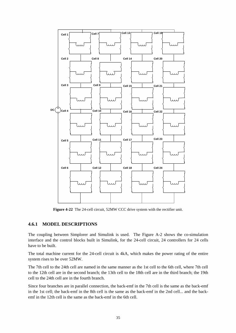
Figure 4-22 The 24-cell circuit, 52MW CCC drive system with the rectifier unit.
4.6.1 MODEL DESCRIPTIONS
The coupling between Simplorer and Simulink is used. The Figure A-2 shows the co-simulation
interface and the control blocks built in Simulink, for the 24-cell circuit, 24 controllers for 24 cells
have to be built.
The total machine current for the 24-cell circuit is 4kA, which makes the power rating of the entire
system rises to be over 52MW.
The 7th cell to the 24th cell are named in the same manner as the 1st cell to the 6th cell, where 7th cell
to the 12th cell are in the second branch; the 13th cell to the 18th cell are in the third branch; the 19th
cell to the 24th cell are in the fourth branch.
Since four branches are in parallel connection, the back-emf in the 7th cell is the same as the back-emf
in the 1st cell; the back-emf in the 8th cell is the same as the back-emf in the 2nd cell... and the back-
emf in the 12th cell is the same as the back-emf in the 6th cell.
36
Also because of the component parameters in the other three branches are the same as the component
parameters in the first branch, the current in each branch should be the same, which is equal to 1kA.
The dc-terminal voltage for the 6-series cells in 24-cell circuit is the same as the voltage in the 6-cell
circuit.
4.6.2 SIMULATION RESULTS
1) The result for the machine current under voltage source
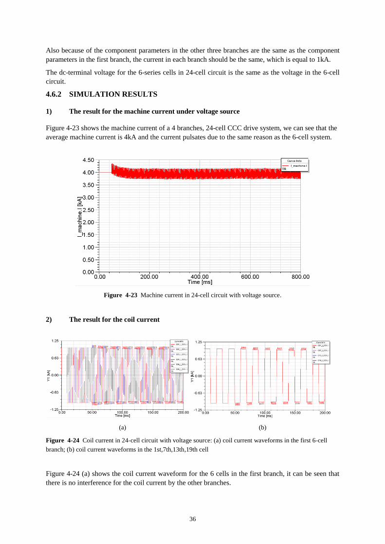
Figure 4-23 shows the machine current of a 4 branches, 24-cell CCC drive system, we can see that the
average machine current is 4kA and the current pulsates due to the same reason as the 6-cell system.
Figure 4-23 Machine current in 24-cell circuit with voltage source.
2) The result for the coil current
(a) (b)
Figure 4-24 Coil current in 24-cell circuit with voltage source: (a) coil current waveforms in the first 6-cell
branch; (b) coil current waveforms in the 1st,7th,13th,19th cell
Figure 4-24 (a) shows the coil current waveform for the 6 cells in the first branch, it can be seen that
there is no interference for the coil current by the other branches.
37
Figure 4-24 (b) shows the coil current waveform in the 1st cell, 7th cell, 13th cell and 19th cell, which
are totally the same, due to the synchronous back-emf in the parallel four cells.
4.6.3 POSSIBLE BENEFITS OF THE PARALLEL SYSTEM
Firstly, by adding more branches, the power rating of the CCC drive system can reach to a
very high value, avoiding to increase the current rating per branch to a high value to achieve
the high power.
Secondly, more branches also means better redundancy of the system, it increases the system
reliability when the fault happens.
Thirdly, making phase shift of the back-emf voltage between each two braches is a possible
way to create a lower ripple of the terminal voltage of the CCC drive system by which means
the reduction of the machine current ripple can be achieved.
4.7 SIMULATION FOR THE CONVERTER CIRCUIT UNDER
ARMATURE REACTION
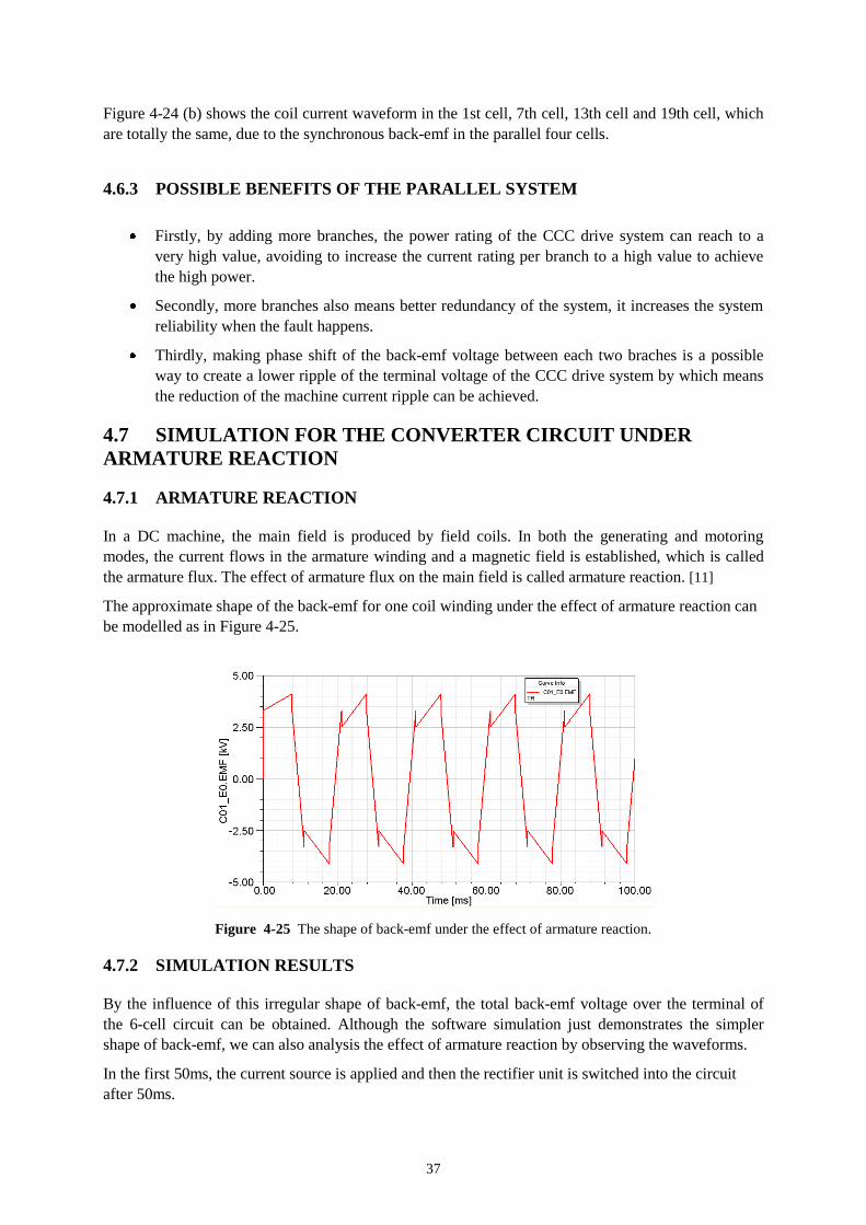
4.7.1 ARMATURE REACTION
In a DC machine, the main field is produced by field coils. In both the generating and motoring
modes, the current flows in the armature winding and a magnetic field is established, which is called
the armature flux. The effect of armature flux on the main field is called armature reaction. [11]
The approximate shape of the back-emf for one coil winding under the effect of armature reaction can
be modelled as in Figure 4-25.
Figure 4-25 The shape of back-emf under the effect of armature reaction.
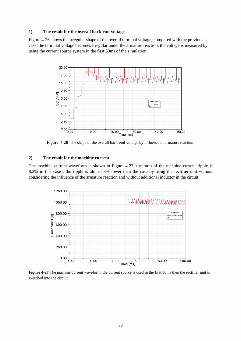
4.7.2 SIMULATION RESULTS
By the influence of this irregular shape of back-emf, the total back-emf voltage over the terminal of
the 6-cell circuit can be obtained. Although the software simulation just demonstrates the simpler
shape of back-emf, we can also analysis the effect of armature reaction by observing the waveforms.
In the first 50ms, the current source is applied and then the rectifier unit is switched into the circuit
after 50ms.
38
1) The result for the overall back-emf voltage
Figure 4-26 shows the irregular shape of the overall terminal voltage, compared with the previous
case, the terminal voltage becomes irregular under the armature reaction, the voltage is measured by
using the current source system in the first 50ms of the simulation.
Figure 4-26 The shape of the overall back-emf voltage by influence of armature reaction.
2) The result for the machine current.
The machine current waveform is shown in Figure 4-27, the ratio of the machine current ripple is
8.3% in this case , the ripple is almost 3% lower than the case by using the rectifier unit without
considering the influence of the armature reaction and without additional inductor in the circuit.
Figure 4-27 The machine current waveform, the current source is used in the first 50ms then the rectifier unit is
switched into the circuit.

39
Thus, this phenomenon of the machine current shows that:
1. The quality of the machine current in this kind of multi-phase system is partly depends on the shape
of back-emf.
2. The simulation by using the circuit analysis software Simplorer is impossible to demonstrate the
real shape of back-emf as well as the machine current.
40
5 POWER LOSSES IN CCC CONVERTER
5.1 INTRODUCTION
The power-dissipation calculation for the IGBTs and diodes is executed by an average computation of
the conduction and switching losses over one period T0 of the output frequency. [12]
The losses in a power-switching semiconductor device consist of three parts:
Conduction losses( condP )
Switching losses( swP )
Blocking losses( bP )
Where the blocking losses normally being neglected.
Thus the total losses=conduction losses + switching losses.
dcI
dci
dci
IGBT1 IGBT2
IGBT3 IGBT4
D1 D2
D3 D4
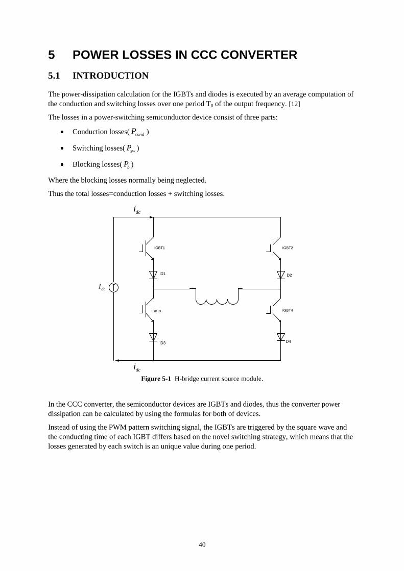
Figure 5-1 H-bridge current source module.
In the CCC converter, the semiconductor devices are IGBTs and diodes, thus the converter power
dissipation can be calculated by using the formulas for both of devices.
Instead of using the PWM pattern switching signal, the IGBTs are triggered by the square wave and
the conducting time of each IGBT differs based on the novel switching strategy, which means that the
losses generated by each switch is an unique value during one period.
41
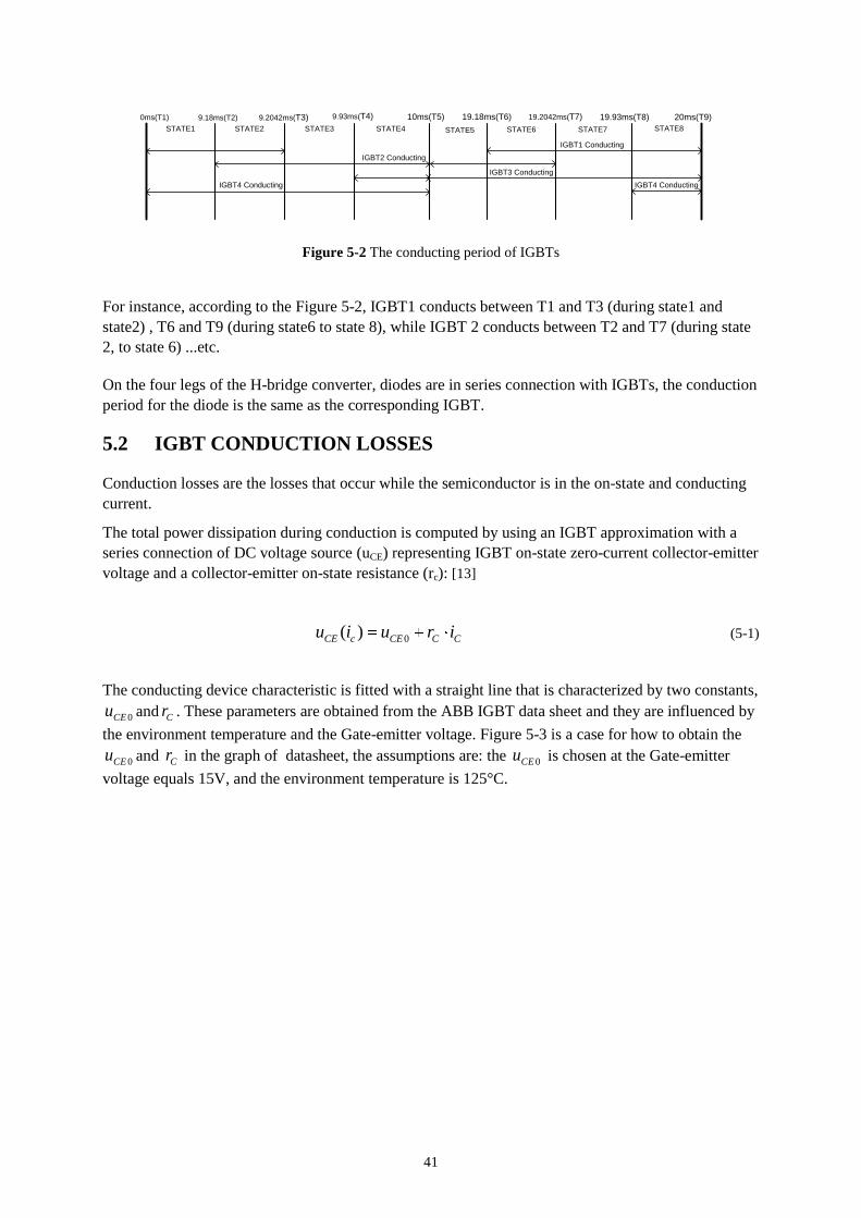
STATE1 STATE2 STATE3 STATE4
IGBT2 Conducting
IGBT3 Conducting
IGBT4 Conducting
0ms(T1) 10ms(T5) 9.18ms(T2)
9.2042ms(T3) 9.93ms(T4)
STATE6 STATE7
19.93ms(T8)
19.2042ms(T7) 19.18ms(T6)
STATE5 STATE8
20ms(T9)
IGBT1 Conducting
IGBT4 Conducting
Figure 5-2 The conducting period of IGBTs
For instance, according to the Figure 5-2, IGBT1 conducts between T1 and T3 (during state1 and
state2) , T6 and T9 (during state6 to state 8), while IGBT 2 conducts between T2 and T7 (during state
2, to state 6) ...etc.
On the four legs of the H-bridge converter, diodes are in series connection with IGBTs, the conduction
period for the diode is the same as the corresponding IGBT.
5.2 IGBT CONDUCTION LOSSES
Conduction losses are the losses that occur while the semiconductor is in the on-state and conducting
current.
The total power dissipation during conduction is computed by using an IGBT approximation with a
series connection of DC voltage source (uCE) representing IGBT on-state zero-current collector-emitter
voltage and a collector-emitter on-state resistance (rc): [13]
0( )CE c CE C Cu i u r i (5-1)
The conducting device characteristic is fitted with a straight line that is characterized by two constants,
0CEu and Cr . These parameters are obtained from the ABB IGBT data sheet and they are influenced by
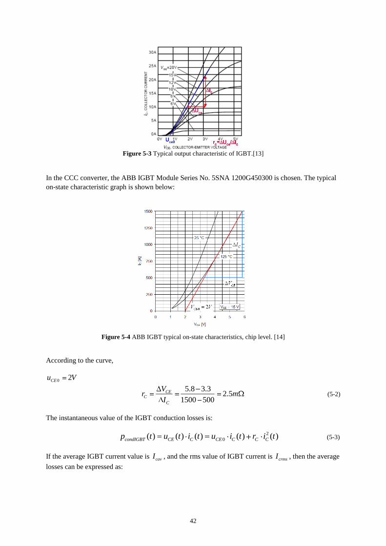
the environment temperature and the Gate-emitter voltage. Figure 5-3 is a case for how to obtain the
0CEu and Cr in the graph of datasheet, the assumptions are: the 0CEu is chosen at the Gate-emitter
voltage equals 15V, and the environment temperature is 125°C.
42
Figure 5-3 Typical output characteristic of IGBT.[13]
In the CCC converter, the ABB IGBT Module Series No. 5SNA 1200G450300 is chosen. The typical
on-state characteristic graph is shown below:
Figure 5-4 ABB IGBT typical on-state characteristics, chip level. [14]
According to the curve,
0 2CEu V
5.8 3.32.5
1500 500
CEC
C
Vr m
I (5-2)
The instantaneous value of the IGBT conduction losses is:
2
0( ) ( ) ( ) ( ) ( )condIGBT CE C CE C C Cp t u t i t u i t r i t (5-3)
If the average IGBT current value is cavI , and the rms value of IGBT current is crmsI , then the average
losses can be expressed as:
43
2 2
0 0
0 0
1 1( ) ( ( ) ( ))
sw swT T
condIGBT condIGBT CE C C C CE cav C crms
sw sw
P p t dt u i t r i t dt u I r IT T
(5-4)
The total IGBT power losses can be obtained by summing the losses on every IGBT (in this case, 4
IGBTs in one cell) together over half a period, since the status of IGBT 1 in the first half period is the
same as the status of IGBT 2 in the second half period, the principle is the same for the IGBT 3 and
IGBT 4. Thus the calculations are just based on the losses in half the period.
The assumption is made that the conducting current through the IGBT1, IGBT2, IGBT3 and IGBT4 is
constant due to the current source, so the average current and the RMS current can be calculated by the
simple formula for these four IGBTs.
Example 5-1 The calculation of the conduction losses in IGBT1
STATE1 STATE2
0ms(T1) 9.2042ms(T3)
IGBT1 Conducting
Figure 5-5 The conducting interval for IGBT1
According to Figure 5-5, IGBT1 conducts between 1T and 3T , which yields:
3 3
11
2 2
1 1 0 0 _ 1 _ 1
1 1( ) ( ( ) ( ))
T
T T
condIGBT condIGBT CE C C C CE cav IGBT C crms IGBT
sw sw T
P p t dt u i t r i t dt u I r IT T
Where swT represents the length of half the period,10ms, here 1T is 0ms, 3T is 9.2042ms.
_ 1
_ 1
9.20421000 920.4200A
10
9.20421000 959.3852
10
cav IGBT
crms IGBT
I
I A
So, the conduction losses for IGBT1 are:
3
1
2
1 1 0 _ 1 _ 1
3 2 3
1( )
(2 920.42 2.5 10 959.3852 ) 4.1419 10
4.1419
T
T
condIGBT condIGBT CE cav IGBT C crms IGBT
sw
P p t dt u I r IT
kW
Using the same method as IGBT1, the conduction losses for the other IGBTs on the legs can be
calculated in the same way and the calculation process can be found in the appendix of the report.
44
Table 5-1 The conduction losses of IGBTs in one cell
Device Conduction Period Conduction Losses Total Losses
IGBT1 T1-T3 4.14kW 9 kW
IGBT2 T2-T5 0.37kW
IGBT3 T4-T5 0.02kW
IGBT4 T1-T5 4.47kW
5.3 DIODE CONDUCTION LOSSES
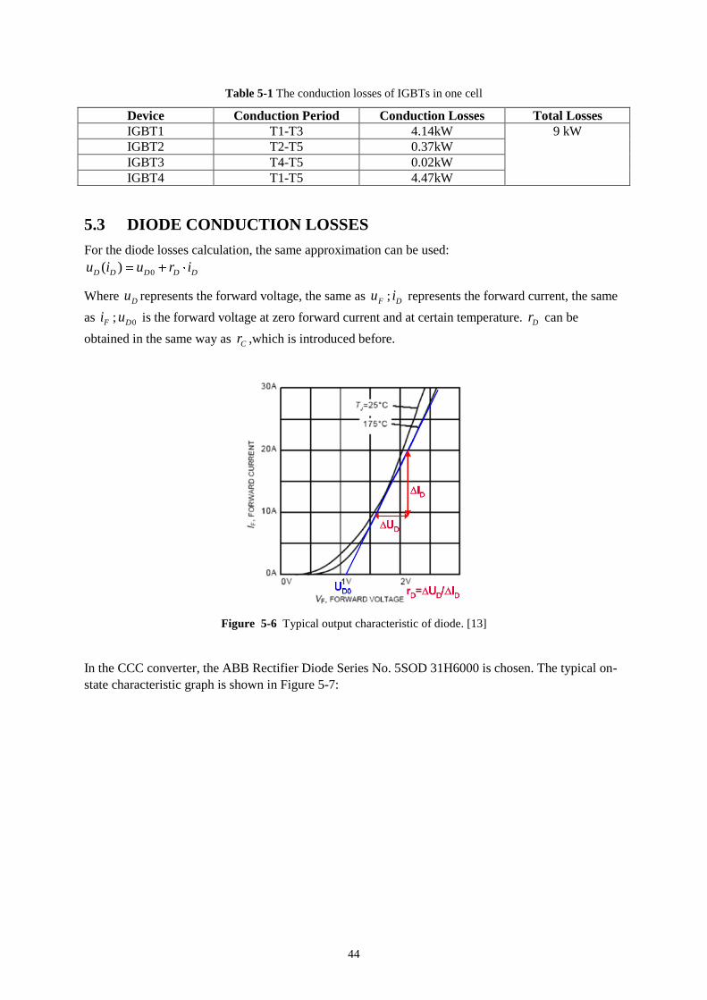
For the diode losses calculation, the same approximation can be used:
0( )D D D D Du i u r i
Where Du represents the forward voltage, the same as Fu ; Di represents the forward current, the same
as Fi ; 0Du is the forward voltage at zero forward current and at certain temperature. Dr can be
obtained in the same way as Cr ,which is introduced before.
Figure 5-6 Typical output characteristic of diode. [13]
In the CCC converter, the ABB Rectifier Diode Series No. 5SOD 31H6000 is chosen. The typical on-
state characteristic graph is shown in Figure 5-7:
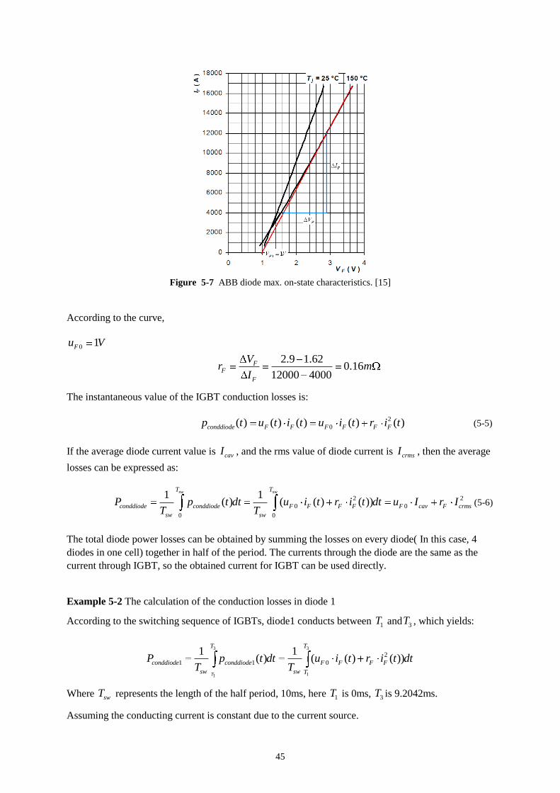
45
Figure 5-7 ABB diode max. on-state characteristics. [15]
According to the curve,
0 1Fu V
2.9 1.62
0.1612000 4000
FF
F
Vr m
I
The instantaneous value of the IGBT conduction losses is:
2
0( ) ( ) ( ) ( ) ( )conddiode F F F F F Fp t u t i t u i t r i t (5-5)
If the average diode current value is cavI , and the rms value of diode current is crmsI , then the average
losses can be expressed as:
2 2
0 0
0 0
1 1( ) ( ( ) ( ))
sw swT T
conddiode conddiode F F F F F cav F crms
sw sw
P p t dt u i t r i t dt u I r IT T
(5-6)
The total diode power losses can be obtained by summing the losses on every diode( In this case, 4
diodes in one cell) together in half of the period. The currents through the diode are the same as the
current through IGBT, so the obtained current for IGBT can be used directly.
Example 5-2 The calculation of the conduction losses in diode 1
According to the switching sequence of IGBTs, diode1 conducts between 1T and 3T , which yields:
3 3
11
2
1 1 0
1 1( ) ( ( ) ( ))
T
T T
conddiode conddiode F F F F
sw sw T
P p t dt u i t r i t dtT T
Where swT represents the length of the half period, 10ms, here 1T is 0ms, 3T is 9.2042ms.
Assuming the conducting current is constant due to the current source.
46
So, the conduction losses are:
3
1
2
1 1 0 _ 1 _ 1
3 2 3
1( )
(1 920.42 0.16 10 959.3852 ) 1.0677 10
1.0677
T
T
conddiode conddiode F cav diode F crms diode
sw
P p t dt u I r IT
kW
Using the same method as diode1, the conduction losses for the other diodes on the bridges can be
calculated in the same way and the calculation process can be check in the appendix of the paper.
Table 5-2 The conduction losses of diodes in one cell
Device Conduction Period Conduction Losses Total Losses
Diode1 T1-T3 1.07kW 2.3208kW
Diode2 T2-T5 0.095kW
Diode3 T4-T5 0.0058kW
Diode4 T1-T5 1.15kW
Thus, the total conduction losses in one commutation cell can be obtained.
Table 5-3 The total conduction losses of semiconductors (IGBT+diode) in one cell
IGBT Conduction losses Diode Conduction losses Total losses
9 kW 2.3208 kW 11.3208kW
5.4 IGBT SWITCHING LOSSES
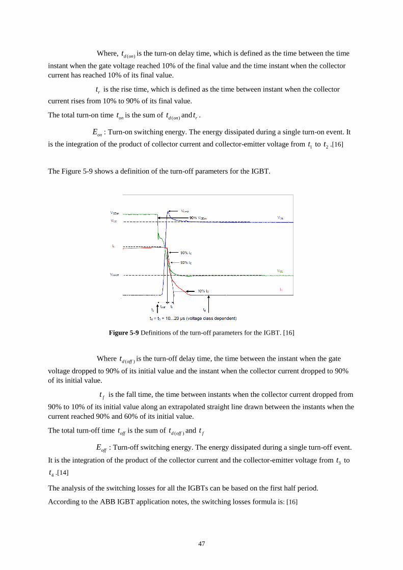
IGBT switching losses is the power dissipation during turn-on and turn-off switching transitions.
Figure 5-8 shows a definition of the turn-on parameters for the IGBT.
Figure 5-8 Definitions of the turn-on parameters for the IGBT. [16]
47
Where, ( )d ont is the turn-on delay time, which is defined as the time between the time
instant when the gate voltage reached 10% of the final value and the time instant when the collector
current has reached 10% of its final value.
rt is the rise time, which is defined as the time between instant when the collector
current rises from 10% to 90% of its final value.
The total turn-on time ont is the sum of ( )d ont and rt .
onE : Turn-on switching energy. The energy dissipated during a single turn-on event. It
is the integration of the product of collector current and collector-emitter voltage from 1t to 2t .[16]
The Figure 5-9 shows a definition of the turn-off parameters for the IGBT.
Figure 5-9 Definitions of the turn-off parameters for the IGBT. [16]
Where ( )d offt is the turn-off delay time, the time between the instant when the gate
voltage dropped to 90% of its initial value and the instant when the collector current dropped to 90%
of its initial value.
ft is the fall time, the time between instants when the collector current dropped from
90% to 10% of its initial value along an extrapolated straight line drawn between the instants when the
current reached 90% and 60% of its initial value.
The total turn-off time offt is the sum of ( )d offt and ft
offE : Turn-off switching energy. The energy dissipated during a single turn-off event.
It is the integration of the product of the collector current and the collector-emitter voltage from 3t to
4t .[14]
The analysis of the switching losses for all the IGBTs can be based on the first half period.
According to the ABB IGBT application notes, the switching losses formula is: [16]
48
6 2 3(5.64 10 9.17 10 1.65) DC
sw on off C C
nom
VE E E I I
V (5-7)
For the turn-off losses, CI can be chosen as the value just before the current transition and DCV can be
treated as the voltage after the transition at the moment the current reduces to zero. nomV is the nominal
voltage which can be obtained in the certain IGBT datasheet.
Example 5-3 The calculation of the turn-off switching losses in IGBT1
According to the switching sequence, IGBT1 conducts during state1 and state2 and then it is switched
off at the beginning of state 3.
The Figure 5-10 shows the IGBT1 turn-off transient and the overlap between voltage and current.
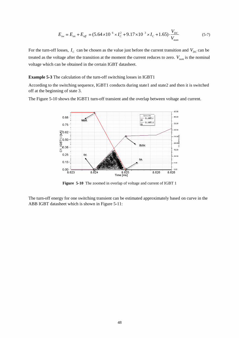
Figure 5-10 The zoomed in overlap of voltage and current of IGBT 1
The turn-off energy for one switching transient can be estimated approximately based on curve in the
ABB IGBT datasheet which is shown in Figure 5-11:
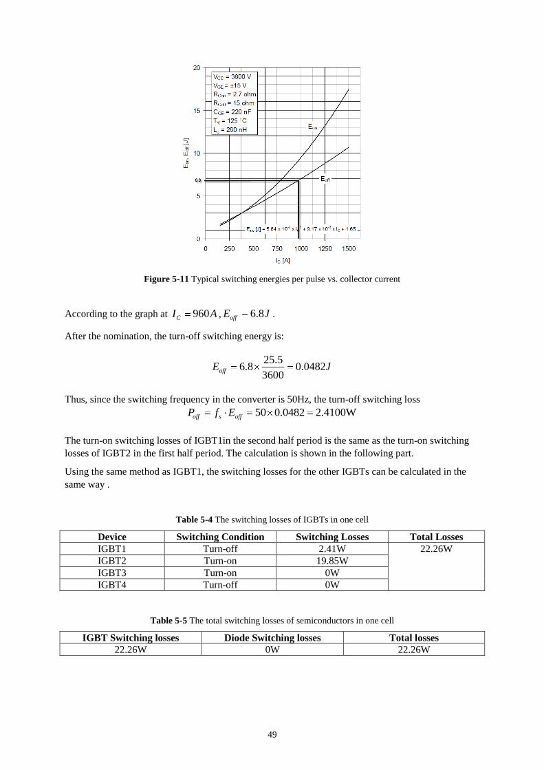
49
Figure 5-11 Typical switching energies per pulse vs. collector current
According to the graph at 960CI A , 6.8offE J .
After the nomination, the turn-off switching energy is:
25.56.8 0.0482
3600offE J
Thus, since the switching frequency in the converter is 50Hz, the turn-off switching loss
50 0.0482 2.4100Woff s offP f E
The turn-on switching losses of IGBT1in the second half period is the same as the turn-on switching
losses of IGBT2 in the first half period. The calculation is shown in the following part.
Using the same method as IGBT1, the switching losses for the other IGBTs can be calculated in the
same way .
Table 5-4 The switching losses of IGBTs in one cell
Device Switching Condition Switching Losses Total Losses
IGBT1 Turn-off 2.41W 22.26W
IGBT2 Turn-on 19.85W
IGBT3 Turn-on 0W
IGBT4 Turn-off 0W
Table 5-5 The total switching losses of semiconductors in one cell
IGBT Switching losses Diode Switching losses Total losses
22.26W 0W 22.26W
50
5.5 FEASIBILITY FOR IGCT - IGCT POWER LOSSES
The ABB's IGCT (Integrated Gate-Commutated Thyristor) has the voltage rating up to 6.5kV and the
current rating 4.2kA; it can be an alternate choice to replace the IGBT in the circuit. IGCT has the
relatively low conduction losses compared to the IGBT; however, economically IGCT is more
expensive than the IGBT at the same rating.
5.5.1 CONDUCTION LOSSES OF IGCT
During the conduction, IGCT is a thyristor and as such it generates substantially lower losses than an
IGBT, which is due to the fact that a transistor operates at much higher charge density than a transistor
due to charge injection from its two emitters (pnp- and npn-transistors). [17]
The calculation of the IGCT conduction losses is similar to the equation for the IGBT, where only the
characteristic parameters are different.
0( )T T T T Tu i u r i (5-8)
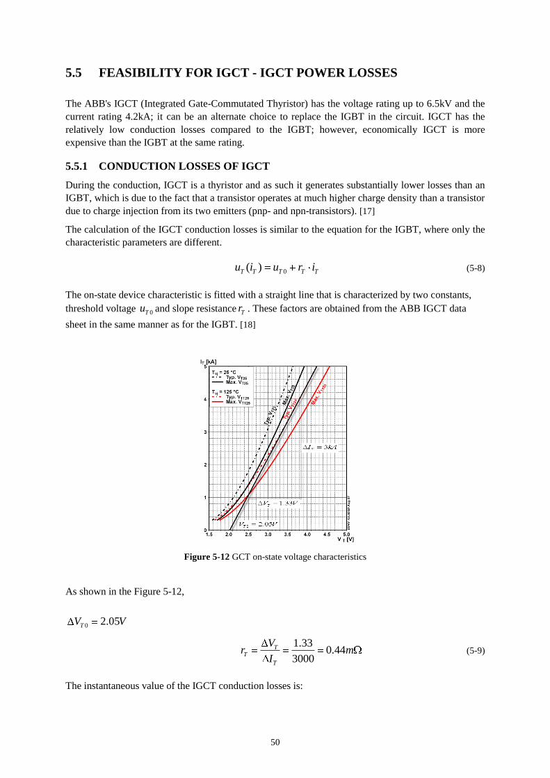
The on-state device characteristic is fitted with a straight line that is characterized by two constants,
threshold voltage 0Tu and slope resistance Tr . These factors are obtained from the ABB IGCT data
sheet in the same manner as for the IGBT. [18]
Figure 5-12 GCT on-state voltage characteristics
As shown in the Figure 5-12,
0 2.05TV V
1.33
0.443000
TT
T
Vr m
I (5-9)
The instantaneous value of the IGCT conduction losses is:
51
2
0( ) ( ) ( ) ( ) ( )IGCT T T T T T Tp t u t i t u i t r i t (5-10)
The same as the IGBT, then the average losses of IGCT can be expressed as:
2 2
0 0
0 0
1 1( ) ( ( ) ( ))
sw swT T
IGCT IGCT T T T T T cav T crms
sw sw
P p t dt u i t r i t dt u I r IT T
(5-11)
Since the calculation procedure of the conduction losses in each IGCT is the same as what has been
done in IGBT, the detailed calculation can be seen in the Appendix B.3
Table 5-6 The conduction losses of IGCTs in one cell
Device Conduction Period Conduction Losses Total Losses
IGCT1 T1-T3 2.29kW 4.9820kW
IGCT2 T2-T5 0.20kW
IGCT3 T4-T5 0.012kW
IGCT4 T1-T5 2.48kW
Table 5-7 The total conduction losses of semiconductors (IGCT+diode) in one cell
IGCT Conduction losses Diode Conduction losses Total losses
4.9820kW 2.3208kW 7.3028W
5.5.2 SWITCHING LOSSES OF IGCT
Since in the Simporer, there is no IGCT model in the model library, the switching losses can be
assumed to be equal to the switching losses of IGBT.
5.6 POWER LOSSES IN THE MULTI-CELL CIRCUIT
The power losses in the IGBT based 6-cell and 24-cell circuit can be calculated, the same as the IGCT
based 6-cell and 24-cell circuit. The calculation results are shown in Table 5-8.
Table 5-8 The total power losses for both the IGBT based and IGCT based multi-cell circuit
Converter Type Circuit type Power range Total power
losses
Power efficiency
IGBT based 6-cell 13.2MW 67.9248kW 99.49%
24-cell 52.8MW 271.6992kW
IGCT based 6-cell 13.2MW 43.8168kW 99.67%
24-cell 52.8MW 175.2672kW
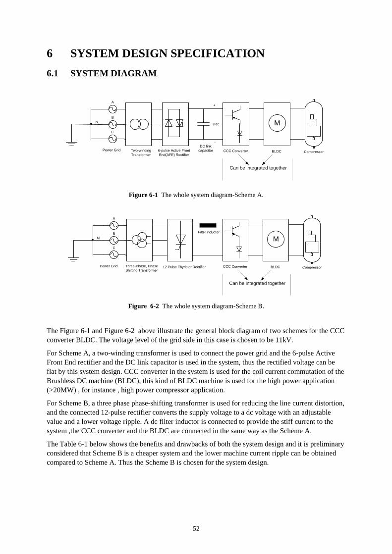
52
6 SYSTEM DESIGN SPECIFICATION
6.1 SYSTEM DIAGRAM
A
B
C
N M
Power Grid Two-winding
Transformer
6-pulse Active Front
End(AFE) RectifierCCC Converter BLDC Compressor
Can be integrated together
+
-
Udc
DC link
capacitor
Figure 6-1 The whole system diagram-Scheme A.
A
B
C
N M
Power Grid Three-Phase, Phase
Shifting Transformer12-Pulse Thyristor Rectifier CCC Converter BLDC Compressor
Can be integrated together
Filter inductor
Figure 6-2 The whole system diagram-Scheme B.
The Figure 6-1 and Figure 6-2 above illustrate the general block diagram of two schemes for the CCC
converter BLDC. The voltage level of the grid side in this case is chosen to be 11kV.
For Scheme A, a two-winding transformer is used to connect the power grid and the 6-pulse Active
Front End rectifier and the DC link capacitor is used in the system, thus the rectified voltage can be
flat by this system design. CCC converter in the system is used for the coil current commutation of the
Brushless DC machine (BLDC), this kind of BLDC machine is used for the high power application
(>20MW) , for instance , high power compressor application.
For Scheme B, a three phase phase-shifting transformer is used for reducing the line current distortion,
and the connected 12-pulse rectifier converts the supply voltage to a dc voltage with an adjustable
value and a lower voltage ripple. A dc filter inductor is connected to provide the stiff current to the
system ,the CCC converter and the BLDC are connected in the same way as the Scheme A.
The Table 6-1 below shows the benefits and drawbacks of both the system design and it is preliminary
considered that Scheme B is a cheaper system and the lower machine current ripple can be obtained
compared to Scheme A. Thus the Scheme B is chosen for the system design.
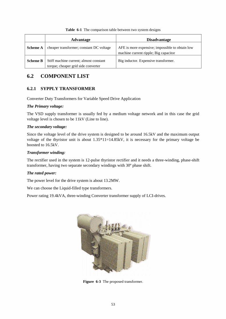
53
Table 6-1 The comparison table between two system designs
Advantage Disadvantage
Scheme A cheaper transformer; constant DC voltage AFE is more expensive; impossible to obtain low
machine current ripple; Big capacitor
Scheme B Stiff machine current; almost constant
torque; cheaper grid side converter
Big inductor. Expensive transformer.
6.2 COMPONENT LIST
6.2.1 SYPPLY TRANSFORMER
Converter Duty Transformers for Variable Speed Drive Application
The Primary voltage:
The VSD supply transformer is usually fed by a medium voltage network and in this case the grid
voltage level is chosen to be 11kV (Line to line).
The secondary voltage:
Since the voltage level of the drive system is designed to be around 16.5kV and the maximum output
voltage of the thyristor unit is about 1.35*11=14.85kV, it is necessary for the primary voltage be
boosted to 16.5kV.
Transformer winding:
The rectifier used in the system is 12-pulse thyristor rectifier and it needs a three-winding, phase-shift
transformer, having two separate secondary windings with 30º phase shift.
The rated power:
The power level for the drive system is about 13.2MW.
We can choose the Liquid-filled type transformers.
Power rating 19.4kVA, three-winding Converter transformer supply of LCI-drives.
Figure 6-3 The proposed transformer.
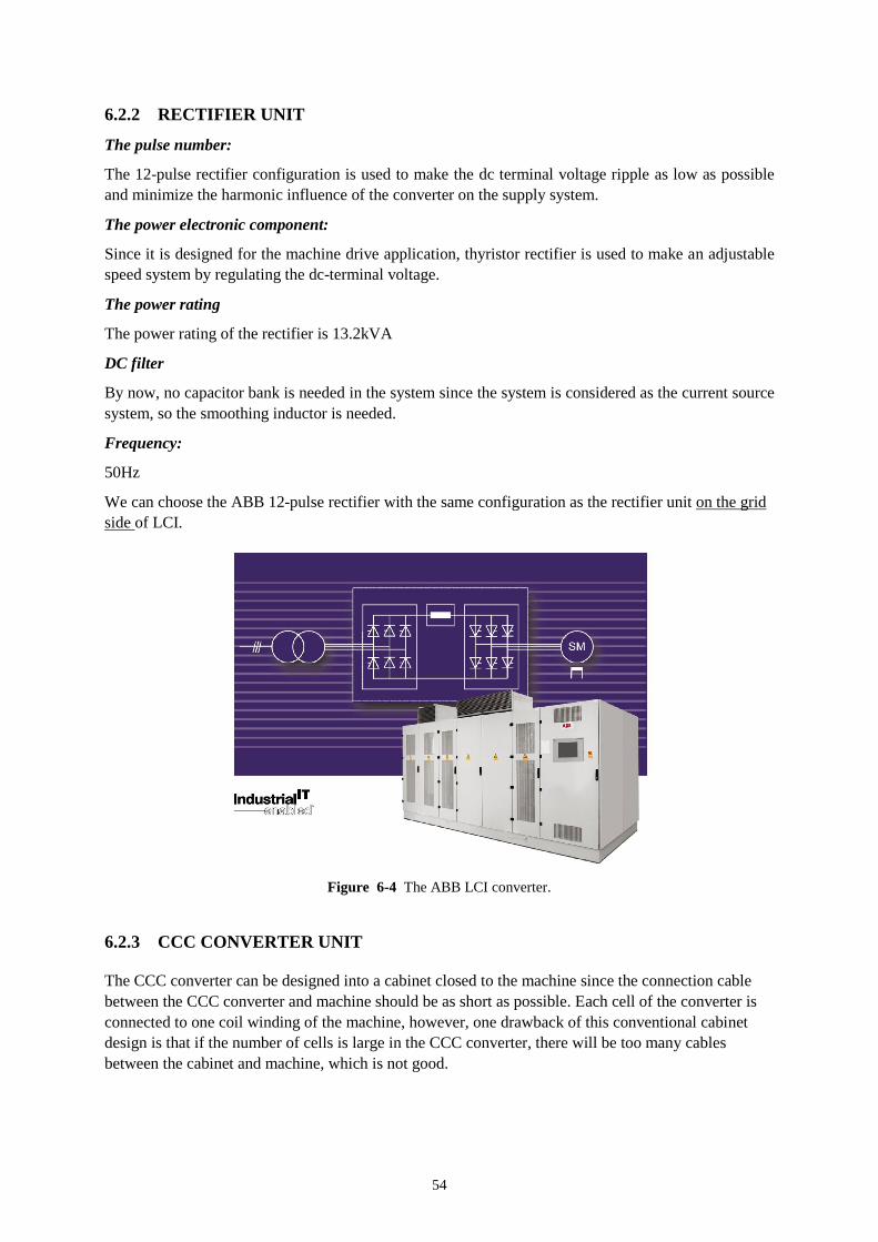
54
6.2.2 RECTIFIER UNIT
The pulse number:
The 12-pulse rectifier configuration is used to make the dc terminal voltage ripple as low as possible
and minimize the harmonic influence of the converter on the supply system.
The power electronic component:
Since it is designed for the machine drive application, thyristor rectifier is used to make an adjustable
speed system by regulating the dc-terminal voltage.
The power rating
The power rating of the rectifier is 13.2kVA
DC filter
By now, no capacitor bank is needed in the system since the system is considered as the current source
system, so the smoothing inductor is needed.
Frequency:
50Hz
We can choose the ABB 12-pulse rectifier with the same configuration as the rectifier unit on the grid
side of LCI.
Figure 6-4 The ABB LCI converter.
6.2.3 CCC CONVERTER UNIT
The CCC converter can be designed into a cabinet closed to the machine since the connection cable
between the CCC converter and machine should be as short as possible. Each cell of the converter is
connected to one coil winding of the machine, however, one drawback of this conventional cabinet
design is that if the number of cells is large in the CCC converter, there will be too many cables
between the cabinet and machine, which is not good.
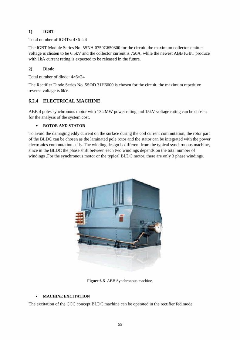
55
1) IGBT
Total number of IGBTs: 4×6=24
The IGBT Module Series No. 5SNA 0750G650300 for the circuit, the maximum collector-emitter
voltage is chosen to be 6.5kV and the collector current is 750A, while the newest ABB IGBT produce
with 1kA current rating is expected to be released in the future.
2) Diode
Total number of diode: 4×6=24
The Rectifier Diode Series No. 5SOD 31H6000 is chosen for the circuit, the maximum repetitive
reverse voltage is 6kV.
6.2.4 ELECTRICAL MACHINE
ABB 4 poles synchronous motor with 13.2MW power rating and 15kV voltage rating can be chosen
for the analysis of the system cost.
ROTOR AND STATOR
To avoid the damaging eddy current on the surface during the coil current commutation, the rotor part
of the BLDC can be chosen as the laminated pole rotor and the stator can be integrated with the power
electronics commutation cells. The winding design is different from the typical synchronous machine,
since in the BLDC the phase shift between each two windings depends on the total number of
windings .For the synchronous motor or the typical BLDC motor, there are only 3 phase windings.
Figure 6-5 ABB Synchronous machine.
MACHINE EXCITATION
The excitation of the CCC concept BLDC machine can be operated in the rectifier fed mode.
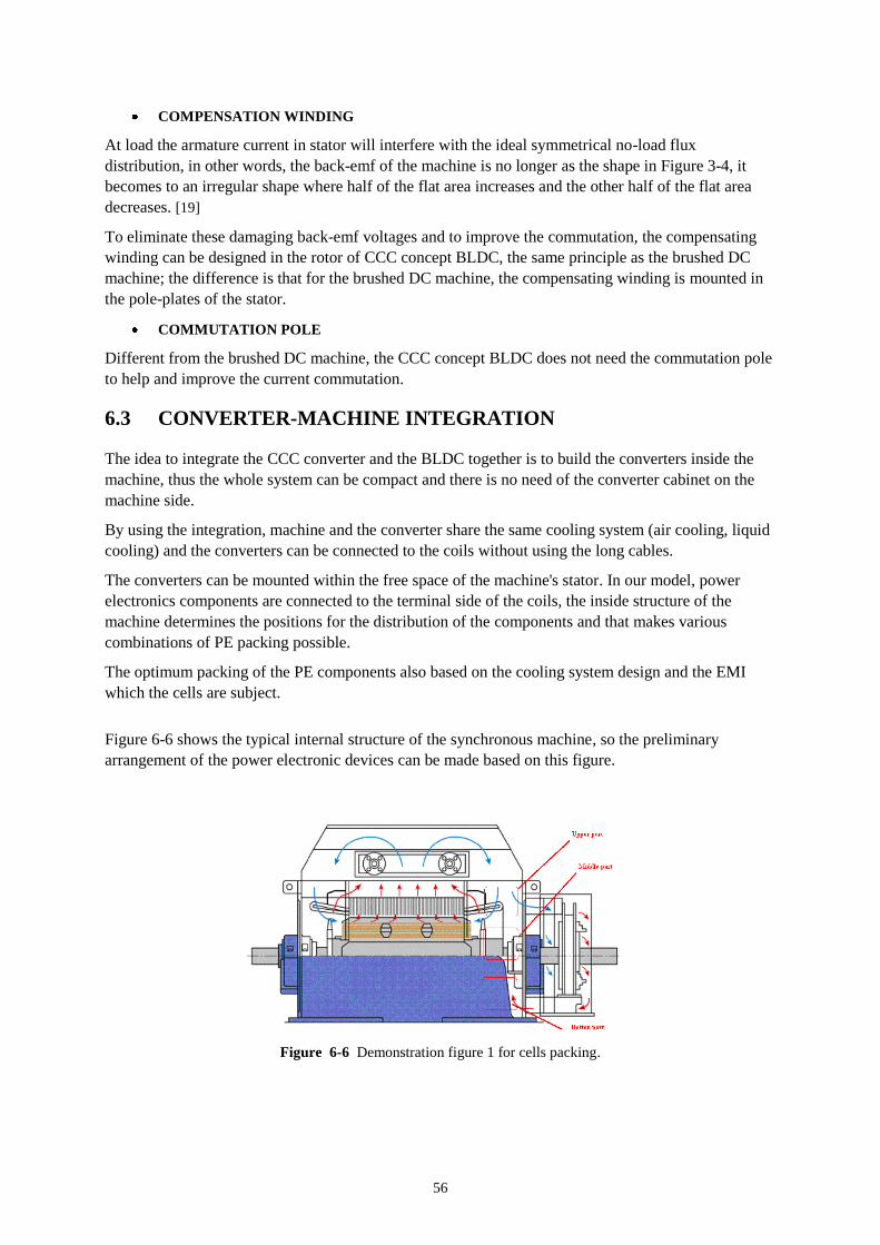
56
COMPENSATION WINDING
At load the armature current in stator will interfere with the ideal symmetrical no-load flux
distribution, in other words, the back-emf of the machine is no longer as the shape in Figure 3-4, it
becomes to an irregular shape where half of the flat area increases and the other half of the flat area
decreases. [19]
To eliminate these damaging back-emf voltages and to improve the commutation, the compensating
winding can be designed in the rotor of CCC concept BLDC, the same principle as the brushed DC
machine; the difference is that for the brushed DC machine, the compensating winding is mounted in
the pole-plates of the stator.
COMMUTATION POLE
Different from the brushed DC machine, the CCC concept BLDC does not need the commutation pole
to help and improve the current commutation.
6.3 CONVERTER-MACHINE INTEGRATION
The idea to integrate the CCC converter and the BLDC together is to build the converters inside the
machine, thus the whole system can be compact and there is no need of the converter cabinet on the
machine side.
By using the integration, machine and the converter share the same cooling system (air cooling, liquid
cooling) and the converters can be connected to the coils without using the long cables.
The converters can be mounted within the free space of the machine's stator. In our model, power
electronics components are connected to the terminal side of the coils, the inside structure of the
machine determines the positions for the distribution of the components and that makes various
combinations of PE packing possible.
The optimum packing of the PE components also based on the cooling system design and the EMI
which the cells are subject.
Figure 6-6 shows the typical internal structure of the synchronous machine, so the preliminary
arrangement of the power electronic devices can be made based on this figure.
Figure 6-6 Demonstration figure 1 for cells packing.
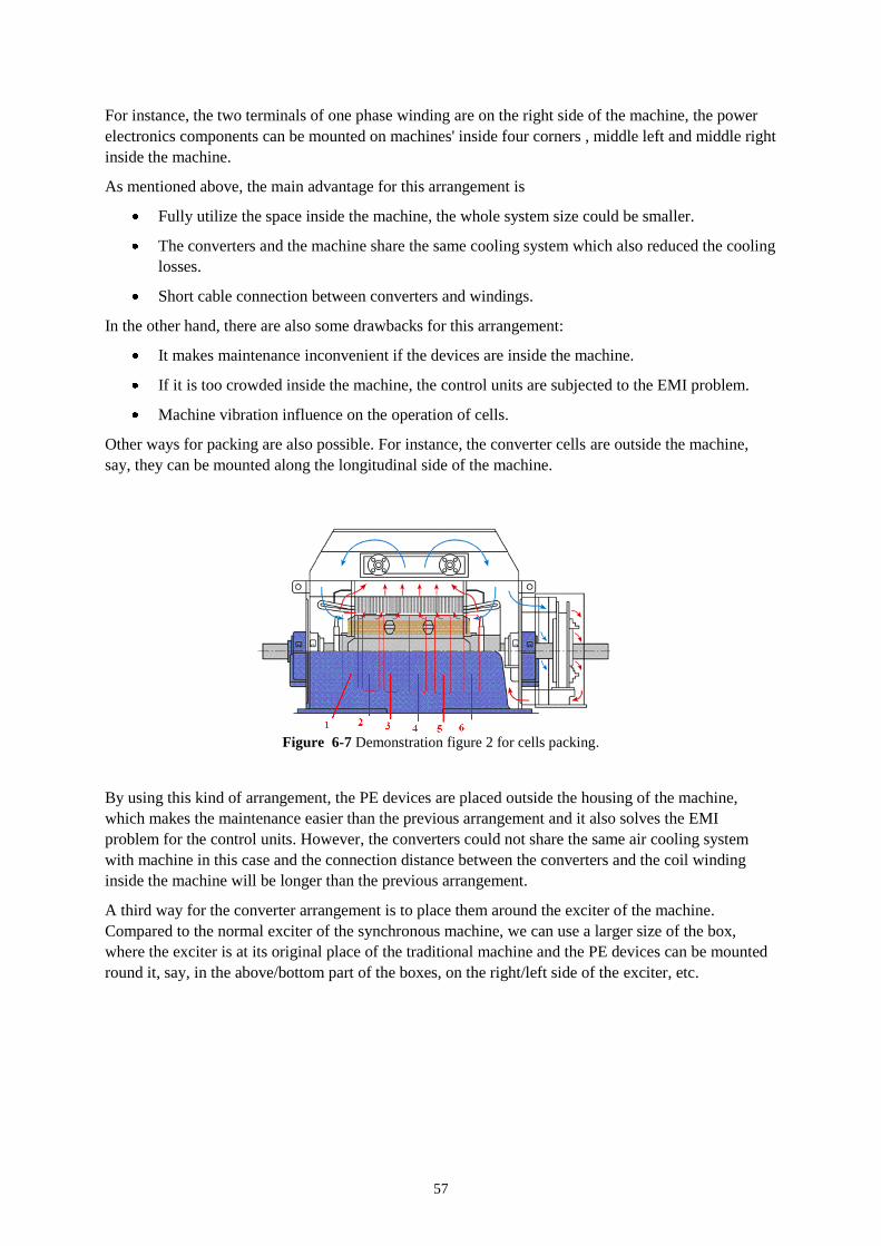
57
For instance, the two terminals of one phase winding are on the right side of the machine, the power
electronics components can be mounted on machines' inside four corners , middle left and middle right
inside the machine.
As mentioned above, the main advantage for this arrangement is
Fully utilize the space inside the machine, the whole system size could be smaller.
The converters and the machine share the same cooling system which also reduced the cooling
losses.
Short cable connection between converters and windings.
In the other hand, there are also some drawbacks for this arrangement:
It makes maintenance inconvenient if the devices are inside the machine.
If it is too crowded inside the machine, the control units are subjected to the EMI problem.
Machine vibration influence on the operation of cells.
Other ways for packing are also possible. For instance, the converter cells are outside the machine,
say, they can be mounted along the longitudinal side of the machine.
Figure 6-7 Demonstration figure 2 for cells packing.
By using this kind of arrangement, the PE devices are placed outside the housing of the machine,
which makes the maintenance easier than the previous arrangement and it also solves the EMI
problem for the control units. However, the converters could not share the same air cooling system
with machine in this case and the connection distance between the converters and the coil winding
inside the machine will be longer than the previous arrangement.
A third way for the converter arrangement is to place them around the exciter of the machine.
Compared to the normal exciter of the synchronous machine, we can use a larger size of the box,
where the exciter is at its original place of the traditional machine and the PE devices can be mounted
round it, say, in the above/bottom part of the boxes, on the right/left side of the exciter, etc.
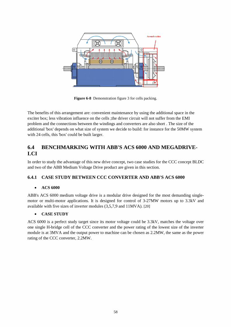
58
Figure 6-8 Demonstration figure 3 for cells packing.
The benefits of this arrangement are: convenient maintenance by using the additional space in the
exciter box; less vibration influence on the cells ;the driver circuit will not suffer from the EMI
problem and the connections between the windings and converters are also short . The size of the
additional 'box' depends on what size of system we decide to build: for instance for the 50MW system
with 24 cells, this 'box' could be built larger.
6.4 BENCHMARKING WITH ABB'S ACS 6000 AND MEGADRIVE-
LCI
In order to study the advantage of this new drive concept, two case studies for the CCC concept BLDC
and two of the ABB Medium Voltage Drive product are given in this section.
6.4.1 CASE STUDY BETWEEN CCC CONVERTER AND ABB'S ACS 6000
ACS 6000
ABB's ACS 6000 medium voltage drive is a modular drive designed for the most demanding single-
motor or multi-motor applications. It is designed for control of 3-27MW motors up to 3.3kV and
available with five sizes of inverter modules (3,5,7,9 and 11MVA). [20]
CASE STUDY
ACS 6000 is a perfect study target since its motor voltage could be 3.3kV, matches the voltage over
one single H-bridge cell of the CCC converter and the power rating of the lowest size of the inverter
module is at 3MVA and the output power to machine can be chosen as 2.2MW, the same as the power
rating of the CCC converter, 2.2MW.
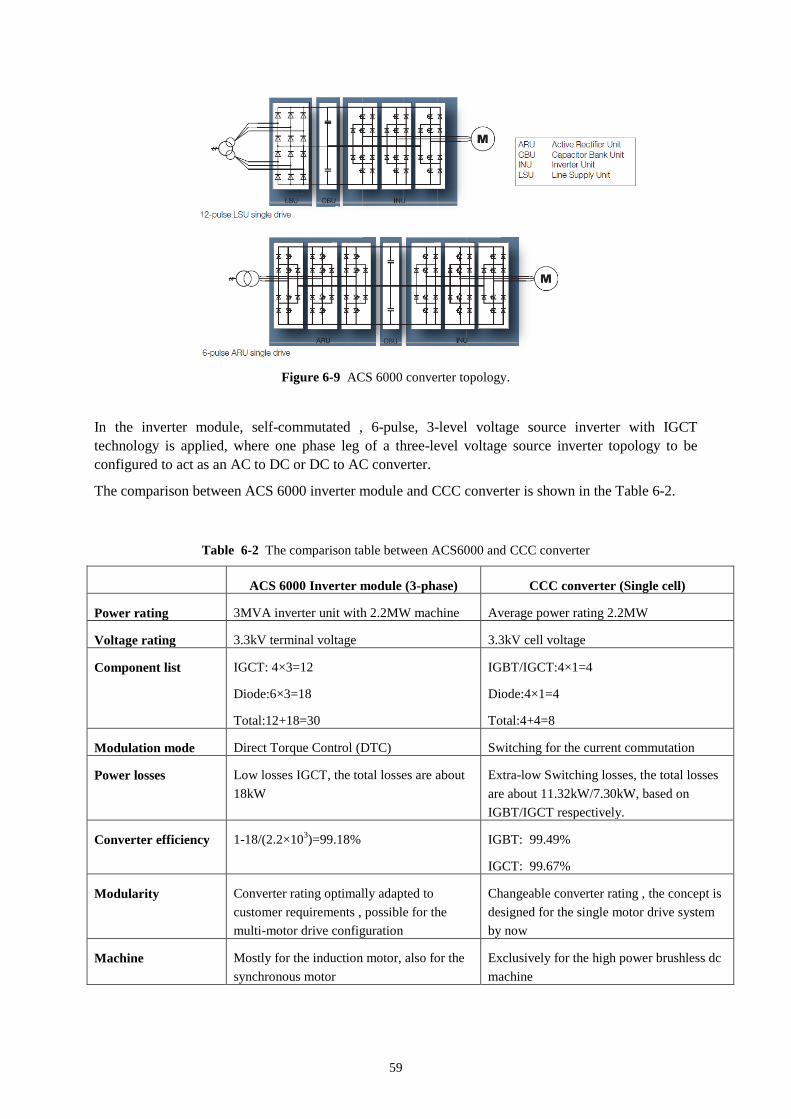
59
Figure 6-9 ACS 6000 converter topology.
In the inverter module, self-commutated , 6-pulse, 3-level voltage source inverter with IGCT
technology is applied, where one phase leg of a three-level voltage source inverter topology to be
configured to act as an AC to DC or DC to AC converter.
The comparison between ACS 6000 inverter module and CCC converter is shown in the Table 6-2.
Table 6-2 The comparison table between ACS6000 and CCC converter
ACS 6000 Inverter module (3-phase) CCC converter (Single cell)
Power rating 3MVA inverter unit with 2.2MW machine Average power rating 2.2MW
Voltage rating 3.3kV terminal voltage 3.3kV cell voltage
Component list IGCT: 4×3=12
Diode:6×3=18
Total:12+18=30
IGBT/IGCT:4×1=4
Diode:4×1=4
Total:4+4=8
Modulation mode Direct Torque Control (DTC) Switching for the current commutation
Power losses Low losses IGCT, the total losses are about
18kW
Extra-low Switching losses, the total losses
are about 11.32kW/7.30kW, based on
IGBT/IGCT respectively.
Converter efficiency 1-18/(2.2×103)=99.18% IGBT: 99.49%
IGCT: 99.67%
Modularity Converter rating optimally adapted to
customer requirements , possible for the
multi-motor drive configuration
Changeable converter rating , the concept is
designed for the single motor drive system
by now
Machine Mostly for the induction motor, also for the
synchronous motor
Exclusively for the high power brushless dc
machine
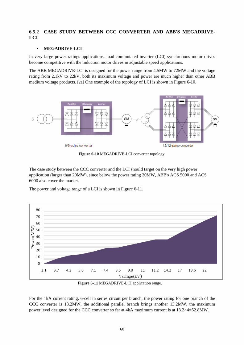
60
6.5.2 CASE STUDY BETWEEN CCC CONVERTER AND ABB'S MEGADRIVE-
LCI
MEGADRIVE-LCI
In very large power ratings applications, load-commutated inverter (LCI) synchronous motor drives
become competitive with the induction motor drives in adjustable speed applications.
The ABB MEGADRIVE-LCI is designed for the power range from 4.5MW to 72MW and the voltage
rating from 2.1kV to 22kV, both its maximum voltage and power are much higher than other ABB
medium voltage products. [21] One example of the topology of LCI is shown in Figure 6-10.
Figure 6-10 MEGADRIVE-LCI converter topology.
The case study between the CCC converter and the LCI should target on the very high power
application (larger than 20MW), since below the power rating 20MW, ABB's ACS 5000 and ACS
6000 also cover the market.
The power and voltage range of a LCI is shown in Figure 6-11.
Figure 6-11 MEGADRIVE-LCI application range.
For the 1kA current rating, 6-cell in series circuit per branch, the power rating for one branch of the
CCC converter is 13.2MW, the additional parallel branch brings another 13.2MW, the maximum
power level designed for the CCC converter so far at 4kA maximum current is at 13.2×4=52.8MW.
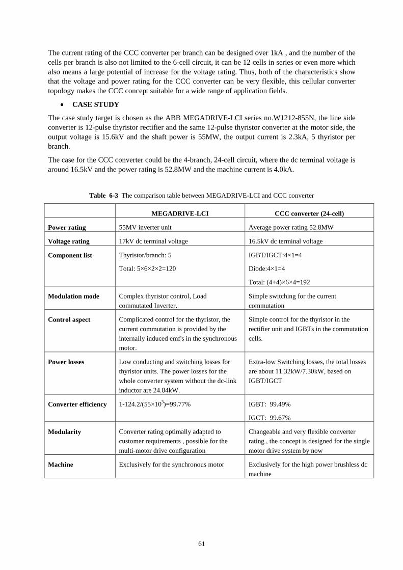
61
The current rating of the CCC converter per branch can be designed over 1kA , and the number of the
cells per branch is also not limited to the 6-cell circuit, it can be 12 cells in series or even more which
also means a large potential of increase for the voltage rating. Thus, both of the characteristics show
that the voltage and power rating for the CCC converter can be very flexible, this cellular converter
topology makes the CCC concept suitable for a wide range of application fields.
CASE STUDY
The case study target is chosen as the ABB MEGADRIVE-LCI series no.W1212-855N, the line side
converter is 12-pulse thyristor rectifier and the same 12-pulse thyristor converter at the motor side, the
output voltage is 15.6kV and the shaft power is 55MW, the output current is 2.3kA, 5 thyristor per
branch.
The case for the CCC converter could be the 4-branch, 24-cell circuit, where the dc terminal voltage is
around 16.5kV and the power rating is 52.8MW and the machine current is 4.0kA.
Table 6-3 The comparison table between MEGADRIVE-LCI and CCC converter
MEGADRIVE-LCI CCC converter (24-cell)
Power rating 55MV inverter unit Average power rating 52.8MW
Voltage rating 17kV dc terminal voltage 16.5kV dc terminal voltage
Component list Thyristor/branch: 5
Total: 5×6×2×2=120
IGBT/IGCT:4×1=4
Diode:4×1=4
Total: (4+4)×6×4=192
Modulation mode Complex thyristor control, Load
commutated Inverter.
Simple switching for the current
commutation
Control aspect Complicated control for the thyristor, the
current commutation is provided by the
internally induced emf's in the synchronous
motor.
Simple control for the thyristor in the
rectifier unit and IGBTs in the commutation
cells.
Power losses Low conducting and switching losses for
thyristor units. The power losses for the
whole converter system without the dc-link
inductor are 24.84kW.
Extra-low Switching losses, the total losses
are about 11.32kW/7.30kW, based on
IGBT/IGCT
Converter efficiency 1-124.2/(55×103)=99.77% IGBT: 99.49%
IGCT: 99.67%
Modularity Converter rating optimally adapted to
customer requirements , possible for the
multi-motor drive configuration
Changeable and very flexible converter
rating , the concept is designed for the single
motor drive system by now
Machine Exclusively for the synchronous motor Exclusively for the high power brushless dc
machine
62
7 CONCLUSIONS AND FUTURE WORK
7.1 CONCLUSION
Comprehensive simulation with Simplorer and Simulink shows the commutation in the CCC
concept works well in different back-emf assumptions.
The system has extremely high level modularity, the converter rating can be designed flexible
due to different requirements.
The system has extremely high efficiency due to the low switching losses.
With the square wave back-emf, the machine has high power density.
Power factor is 1.0 of CCC converter.
Low converter losses makes it possible to integrate the inverter attached to the machine.
7.2 FUTURE WORK
Because of the thesis work only focused on the converter topology of the CCC drive system,
more efforts can be made by using the co-simulation between Simplorer and Maxwell,
coupling the converter model and the machine model together to check the operating
behaviour under using the realistic model.
The cooling solution for the commutation converters and the machine in this integrated
machine concept should be studied .
More efforts should be made on the aspect of the machine winding design and its inner
structure optimization, the excitation system design, the calculation of the machine losses.
The cost of the whole system is not well discussed in this thesis due to the limitation of the
sources so more efforts should be made to check the feasibility of the CCC drive system.
63
Reference
[1] Marc Hiller, Rainer Sommer, Max Beuermann , Medium Voltage Drives, IEEE Industry
Applications Magazine MAR|APR 2010.
[2] Brushless DC Motor Fundamentals, AN885,Microchip Technology Inc.
[3] Simulation Study of an Electronically Commutated DC Machine, Marcus L. Grahan and
Sheldon Gruber. IEEE transactions on industrial electronics ,vol.IE-32.no.4, November 1985
[4] F. Caricchi, F. Crescimbini, F. Giulii Capponi, L. Solero, "A Novel Solid-State-Commutator
PM Motor - Arrangement for EV Application". IAS Annual meeting, p2545-2551, 1999
[5] Zhiguo “Zach” Pan, Raed Ahmad and Daniel M. Saban, Space-Shifted Split-Phase High-
Speed Motor/Converter Topology with Fault-Tolerance Capability," IAS08, 2008
[6] Converteam, "Electronic Commutation Circuit", European Patent Application, EP1798847A2,
Publ. 2007
[7] CONVERTEAM, 'Advanced Propulsion Motor'.
[8] Simplorer- System Simulation Software for Multi-Domain Design
[9] http://www.mathworks.com/products/matlab/
[10] http://www.mathworks.com/products/simulink/
[11] http://en.wikipedia.org/wiki/Armature_(electrical_engineering)#Armature reaction in a DC
machine
[12] IEC 60146 "Semiconductor converters"
[13] IGBT Power Losses Calculation Using the Data-Sheet Parameters by Dr.Dusan Graovac,
Marco Purschel, Automotive Power
[14] IGBT Module 5SNA 0750G650300 ABB product datasheet, ABB Switzerland Ltd,
Semiconductors.
[15] Rectifier Diode 5SDD 31H6000 ABB product datasheet, ABB Switzerland Ltd,
Semiconductors.
[16] Applying IGBTs, Application Note. Björn Backlund, Raffael Schnell, Ulrich Schlapbach,
Roland Fischer, Evgeny Tsyplakov. ABB Switzerland Ltd Semiconductors April 09.
[17] Asymmetric Integrated Gate-Commutated Thyristor 5SHY 42L6500
[18] Application Specific IGCTs, Eric Carroll, Bjoern Oedegard, Thomas Stiasny, Marco
Rossinelli, ABB Semiconductors AG.
[19] Electrical Machines and Drives, KTH Electrical Machines and Power Electronics, Stockholm
2009.
[20] ACS 6000 Brochure, www.abb.com
[21] Medium Voltage AC Drives, Product overview. ABB
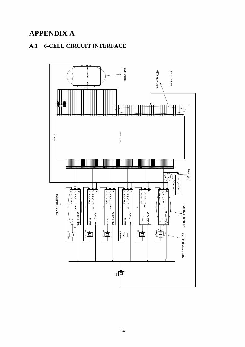
64
APPENDIX A
A.1 6-CELL CIRCUIT INTERFACE
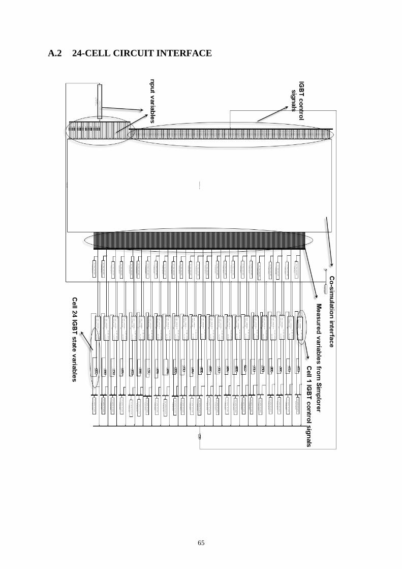
65
A.2 24-CELL CIRCUIT INTERFACE
66
APPENDIX B
CALCULATION OF SEMICONDUCTOR LOSSES
B.1 IGBT CONDUCTION LOSSES
1.The conduction losses of IGBT 1 is calculated in Chapter 5.
2. The conduction losses in IGBT 2
Based on the same principle, IGBT 2 conducts between 2T and 5T , where 2T is 9.18ms , 5T is 10ms
and 10swT ms .
_ 2
_ 2
10 9.181000 82A
10
10 9.181000 286.3564A
10
cav IGBT
crms IGBT
I
I
Thus the conduction losses are:
5
2
2
2 2 0 _ 2 _ 2
3 2
1( )
(2 82 2.5 10 286.3564 ) 369.0000
0.369
T
T
condIGBT condIGBT CE cav IGBT C crms IGBT
sw
P p t dt u I r IT
kW
3. The conduction losses in IGBT 3
IGBT 3 conducts between 4T and 5T , where 4T is 9.93ms , 5T is 10ms and 10swT ms .During the
conduction period, the constant current is about 742A due to the other part of current flows through
IGBT 4.
_ 3
_ 3
10 9.93742 5.1940A
10
10 9.93742 62.0802A
10
cav IGBT
crms IGBT
I
I
The conduction losses are:
5
4
2
3 3 0 _ 3 _ 3
3 2
1( )
(2 5.1940 2.5 10 62.0802 ) 20.0229
0.020
T
T
condIGBT condIGBT CE cav IGBT C crms IGBT
sw
P p t dt u I r IT
kW
4. The conduction losses in IGBT 4
IGBT 4 conducts between 1T and 5T , where 1T is 0ms , 5T is 10ms and 10swT ms . During the
conduction period of IGBT 3, the constant current is about (1000-742)A due to the other part of
current flows through IGBT 3.
67
_ 4
2 2
_ 4
9.93 1000 (10 9.93) (1000 742)994.8060A
10
9.93 1000 (10 9.93) (1000 742) 996.7276A
10
cav IGBT
crms IGBT
I
I
The conduction losses are:
5
1
2
4 4 0 _ 4 _ 4
3 2 3
1( )
(2 994.8060 2.5 10 996.7276 ) 4.4733 10
4.4733
T
T
condIGBT condIGBT CE cav IGBT C crms IGBT
sw
P p t dt u I r IT
kW
68
B.2 DIODE CONDUCTION LOSSES
1.The conduction losses in diode 1 is calculated in Chapter 9.
2. The conduction losses in diode 2
Based on the same principle, diode 2 conducts between 2T and 5T , where 2T is 9.18ms , 5T is 10ms
and 10swT ms .
Thus the conduction losses are:
5
2
2
2 2 0 _ 2 _ 2
3 2
1( )
(1 82 0.16 10 286.3564 ) 95.1200
0.09512
T
T
conddiode conddiode CE cav diode C crms diode
sw
P p t dt u I r IT
kW
3. The conduction losses in diode 3
Diode 3 conducts between 4T and 5T , where 4T is 9.93ms , 5T is 10ms and 10swT ms .
The conduction losses are:
5
4
2
3 3 0 _ 3 _ 3
3 2
1( )
(1 5.1940 0.16 10 62.0802 ) 5.8106
0.00581
T
T
conddiode conddiode CE cav diode C crms diode
sw
P p t dt u I r IT
kW
4. The conduction losses in diode 4
Diode 4 conducts between 1T and 5T , where 1T is 0ms , 5T is 10ms and 10swT ms .
The conduction losses are:
5
1
2
4 4 _ 4 _ 4
3 2 3
1( )
(1 994.8060 0.16 10 996.7276 ) 1.1538 10
1.1538
T
T
conddiode conddiode F cav diode F crms diode
sw
P p t dt u I r IT
kW
69
B.3 IGCT CONDUCTION LOSSES
1.The conduction losses of IGCT 1
The same as by using the IGBT 1, IGCT 1 conducts between 1T and 3T , the conduction losses for
IGCT 1 are: 3
1
2
1 1 0 _ 1 _ 1
3 2 3
1( )
(2.05 920.42 0.44 10 959.3852 ) 2.2918 10
2.2918
T
T
condIGCT condIGCT T cav IGCT T crms IGCT
sw
P p t dt V I r IT
kW
2. The conduction losses in IGCT 2
Based on the same principle, IGCT 2 conducts between 2T and 5T , where 2T is 9.18ms , 5T is 10ms
and 10swT ms .
Thus the conduction losses are:
5
2
2
2 2 0 _ 2 _ 2
3 2
1( )
(2.05 82 0.44 10 286.3564 ) 204.1800
0.204
T
T
condIGCT condIGCT T cav IGCT T crms IGCT
sw
P p t dt u I r IT
kW
3. The conduction losses in IGCT 3
IGCT 3 conducts between 4T and 5T , where 4T is 9.93ms , 5T is 10ms and 10swT ms .During the
conduction period, the constant current is about 742A due to the other part of current flows through
IGCT 4.
The conduction losses are:
5
4
2
3 3 0 _ 3 _ 3
3 2
1( )
(2.05 5.1940 0.44 10 62.0802 ) 12.3434
0.012
T
T
condIGCT condIGCT T cav IGCT T crms IGCT
sw
P p t dt u I r IT
kW
4. The conduction losses in IGCT 4
IGCT 4 conducts between 1T and 5T , where 1T is 0ms , 5T is 10ms and 10swT ms . During the
conduction period of IGCT 3, the constant current is about (1000-742)A due to the other part of
current flows through IGCT 3.
The conduction losses are:
5
1
2
4 4 0 _ 4 _ 4
3 2 3
1( )
(2.05 994.8060 0.44 10 996.7276 ) 2.4765 10
2.4765
T
T
condIGCT condIGCT T cav IGCT T crms IGCT
sw
P p t dt u I r IT
kW
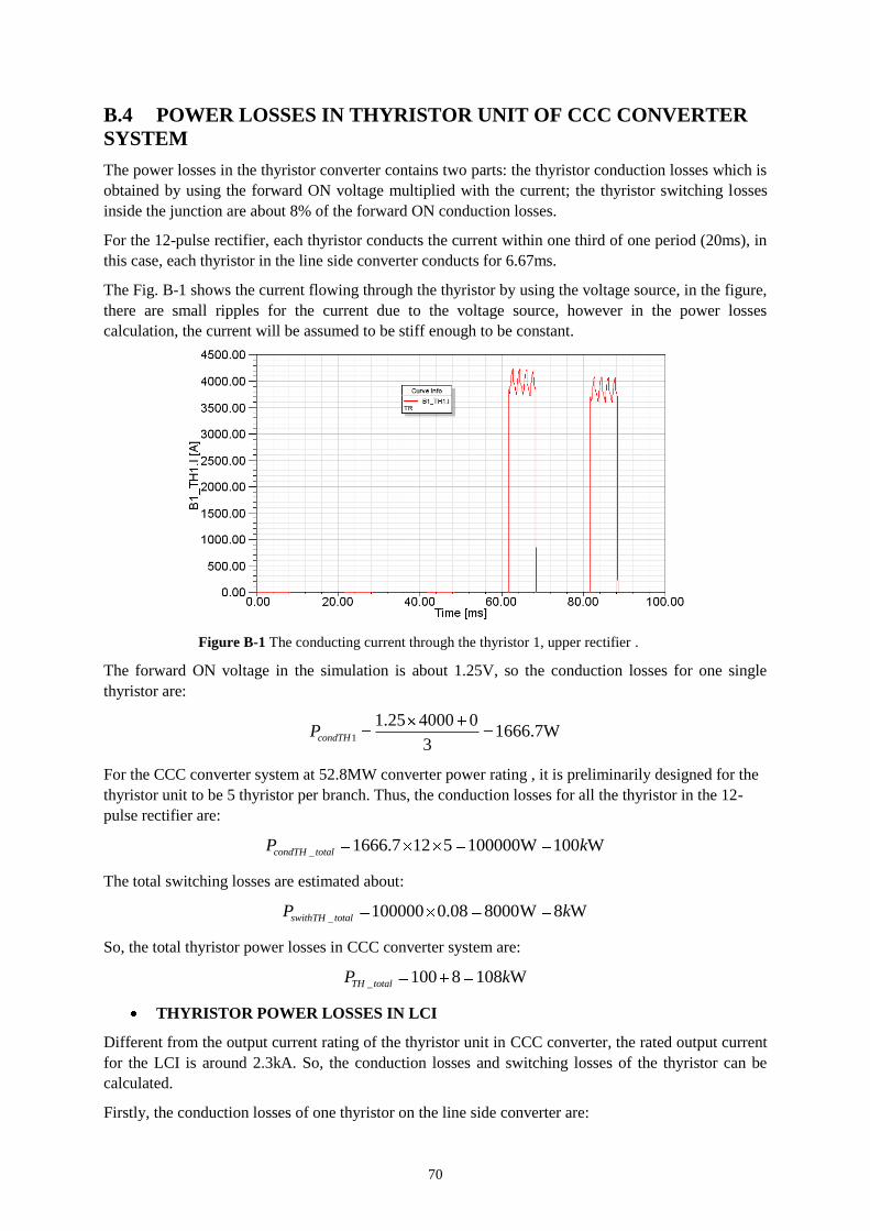
70
B.4 POWER LOSSES IN THYRISTOR UNIT OF CCC CONVERTER
SYSTEM
The power losses in the thyristor converter contains two parts: the thyristor conduction losses which is
obtained by using the forward ON voltage multiplied with the current; the thyristor switching losses
inside the junction are about 8% of the forward ON conduction losses.
For the 12-pulse rectifier, each thyristor conducts the current within one third of one period (20ms), in
this case, each thyristor in the line side converter conducts for 6.67ms.
The Fig. B-1 shows the current flowing through the thyristor by using the voltage source, in the figure,
there are small ripples for the current due to the voltage source, however in the power losses
calculation, the current will be assumed to be stiff enough to be constant.
Figure B-1 The conducting current through the thyristor 1, upper rectifier .
The forward ON voltage in the simulation is about 1.25V, so the conduction losses for one single
thyristor are:
1
1.25 4000 01666.7W
3condTHP
For the CCC converter system at 52.8MW converter power rating , it is preliminarily designed for the
thyristor unit to be 5 thyristor per branch. Thus, the conduction losses for all the thyristor in the 12-
pulse rectifier are:
_ 1666.7 12 5 100000W 100 WcondTH totalP k
The total switching losses are estimated about:
_ 100000 0.08 8000W 8 WswithTH totalP k
So, the total thyristor power losses in CCC converter system are:
_ 100 8 108 WTH totalP k
THYRISTOR POWER LOSSES IN LCI
Different from the output current rating of the thyristor unit in CCC converter, the rated output current
for the LCI is around 2.3kA. So, the conduction losses and switching losses of the thyristor can be
calculated.
Firstly, the conduction losses of one thyristor on the line side converter are:
71
1
1.25 2300 0958.3333W
3condTHP
Then, the conduction losses for all the thyristor in the line side 12-pulse converter are:
_ 958.3333 12 5 57500W 57.5 WcondTH linetotalP k
The total switching losses in the line side converter are:
_ 57500 0.08 4600W 4.6 WswithTH linetotalP k
Finally, the total thyristor power losses in the line side converter are:
_ 57.5 4.6 62.1 WTH linetotalP k
The power losses in the motor side converter is estimated to be the same as the losses in the line side
converter, so the total power losses in the LCI converter are:
_ 62.1 2 124.2 WTH totalP k
The LCI converter efficiency is:
124.21 99.77%
55000LCIconverter
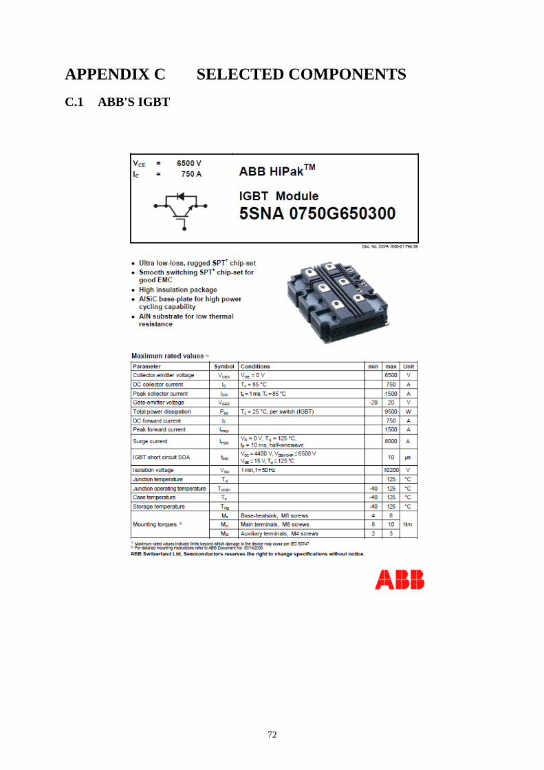
72
APPENDIX C SELECTED COMPONENTS
C.1 ABB'S IGBT
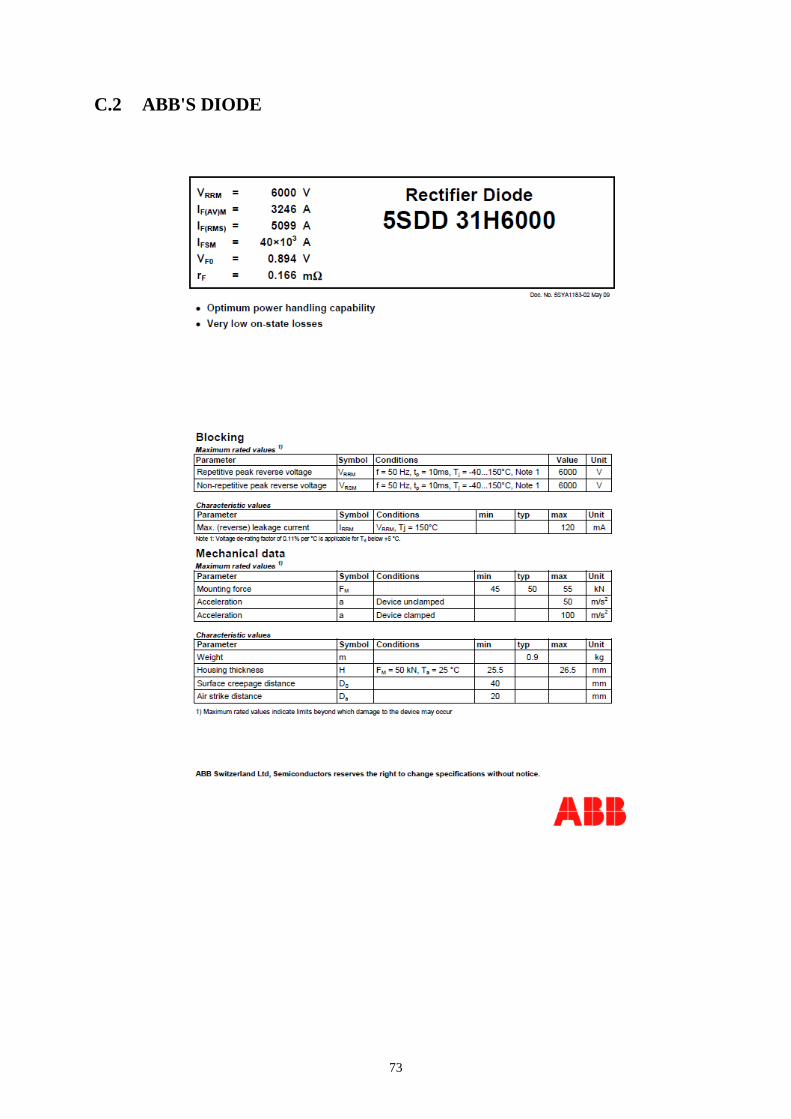
73
C.2 ABB'S DIODE
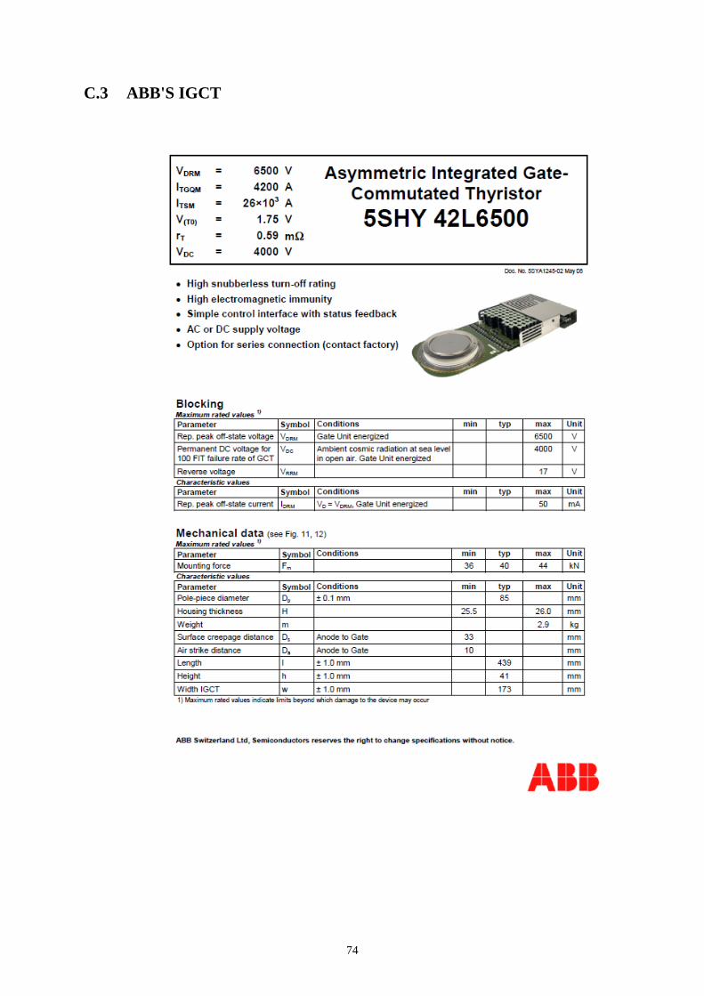
74
C.3 ABB'S IGCT