Embed Size (px)
Citation preview
Research ArticleXPS Depth Study on the Liquid Oxidation of Sn-Bi-Zn-X(AlP)Alloy and the Effect of AlP on the Film
X J Wang1 N Liu1 S Shi1 and Y X Chen2
1School of Material and Science Engineering Jiangsu University of Science and Technology Zhenjiang 212003 China2School of Mechanical and Electrical Engineering Shanghai Dianji University Shanghai 201306 China
Correspondence should be addressed to X J Wang xjwang0163com and Y X Chen cyx1978yeahnet
Received 7 April 2015 Revised 20 June 2015 Accepted 22 June 2015
Academic Editor Aziz Dinia
Copyright copy 2015 X J Wang et al This is an open access article distributed under the Creative Commons Attribution Licensewhich permits unrestricted use distribution and reproduction in any medium provided the original work is properly cited
X-ray photoelectron spectroscopy (XPS) was used to study the properties of liquid oxidation of Sn-Bi-Zn (SBZ) solder alloys andthe effect of AlP on the oxide film The results showed that the oxidation film on SBZ surface was in high concentration of bothoxygen and zinc Adding trace amount of AlP to SBZ alloys (SBZAABZP) decreased the ratio ofOM (Mcould be Sn Bi andAlP)and changed the film compositions Layers near the free surface of oxidation filmmostly contained Zn2+ and Al3+ oxides for SBZAFrom the half quantitative analysis result the aluminum had a surface enrichment behavior in liquid solder so did phosphorus andzinc Therefore the AlP addition changed their stoichiometry such as the ratio of OM near film surface
1 Introduction
Due to the step-soldering process in electronic package sol-der alloys joining at different temperature ranges have been indemand duringmanufacturing procedure Sn-Ag-Cu systemnotably Sn-30Ag-05Cu has been becoming themain streamin surface mount technology (SMT) as a middle-temperaturePb-free solder Accordingly Sn-Bi alloy represented by eutec-tic Sn-58Bi has been used for thermal module connectionin notebook ascribed to the low cost superior wettabilityand almost void-free bonding [1ndash3] It can also reduce thedamage arising from the mismatch of thermal expansionamong various components in electronic assembly [1]
But there are still two issues preventing further appli-cation of Sn-Bi alloy that is lower thermal conductivityand microstructure coarsening with a serious Bi segregationalong the interface which can greatly decrease the reliabilityof the solder joint [4] Actually decreasing Bi-content hasbeen an effective way to adjust the thermal conductivityand melting range As for the microstructure instability atsoldering temperature can be suppressed by incorporatingfine dispersoid particles into Sn-Bi alloy [4 5]
Among the alloying elements Zn Al and P are verycheap and useful It is reported that minor Zn doped in Pb-free solders can obviously inhibit the growth of intermetalliccompounds (IMCs) restrain the growth of Cu
3Sn and
suppress the formation of Kirkendall voids during isothermalaging [6 7] About 05 wt Zn addition to Sn-Ag-Cu-Cesolder alloy can restrain the growth of tin whiskers andstrengthen the solder joints [8] Being very active Zn willworsen the oxidation performance of solder alloy during andafter soldering Element alloying has been an effective wayto improve the antioxidant power of Zn-containing solders[9] Al Ag and In addition can improve the liquid oxidationbehavior at Sn-Zn alloy [9ndash12] Furthermore Al decreases theoxidation rate while doping in Sn-Zn alloy due to the forma-tion of Al
2O3thin film on the surface which is much similar
to Bi Ga and P for Sn-Zn solders [12] Since Al and P havebeen paidmuch attention for the cheapness and effectivenessSn-40Bi-2Zn (SBZ) and Sn-40Bi-2Zn-X (X could beAl and Psimplified as SBZA and SBZP resp) will be used to investigatethe effect of minor AlP addition on the oxidation perfor-mance of SBZ alloy As regards the testingmethod using XPSin the characterization of formed metal alloy surface is not
Hindawi Publishing CorporationAdvances in Materials Science and EngineeringVolume 2015 Article ID 257231 10 pageshttpdxdoiorg1011552015257231
2 Advances in Materials Science and Engineering
new [13 14] Many efforts focusing on oxide formation oniron steel and molten tin have been implemented [13ndash15]
2 Experimental Procedures
21 Preparation of Specimens SBZ SBZA SBZP and Sn-58Bialloys (for comparison in oxidation observation by eye) wereprepared using pure Sn Bi Zn Al and P in vacuum ovenat 800∘C and remelted with stirring at 200∘C to obtain ahomogenized solder alloy During the remelting process anantioxidation agent was used to protect the liquid solder fromoxidation Subsequently the solder alloys were aged for twoweeks in room temperature for a stabilized microstructure
22 Surface Observation of Solder Alloy after OxidationAbout 40 g solder alloys were put in graphite crucibles with adiameter of 28mm and heated up to 170 plusmn 5∘C to observe theoxidation processes during 1 h in air The first dross shouldbe carefully scraped away from the initial liquid surface toleave a fresh surface for oxidation starting therefrom Thecolor changes of the liquid solder surface with oxidation timeincreasing were observed visually and the final appearance ofthe oxide films was recorded by a digital camera
23 XPS Procedure Solder alloys were exposed at 170 plusmn 5∘Cfor 7min before cooling down to achieve oxidized surfacesThe solid samples were cut from the top surface of the ingotsinto about 2-3mm sheets for XPS tests For the test is sensitiveto pollution all the samples should be kept carefully awayfrom contaminations
The surface elementary and chemical analyses were car-ried out via XPS with an achromatic Al K
120572X-ray source
After the original surface of samples was analyzed an argonion beam with 02 120583A current operating at 3 keV was used toetch away a very thin layer of the solder from the oxidationsurface to expose the underlying layer Subsequently a secondsurface analysis of the newer oxide film was performed byXPS with an argon gun attached to So repeatedly an etchrate of about 06 nms was motivated over a 2mm times 2mmarea by the manner the same as [16]
24 XSP Data Analysis The etching and measurement foreach sample were operated about 10 times till the oxygencontent test on the surface becomes near to zero All thespectra were calibrated by carbon adsorbed on the initialsurface of the sample during etching
Curve fitting processes for all high-resolution spectrawere implemented by the XPS Peak-Fitting Programme-XPSPEAK41 to deconvolute and quantify the contributionof each chemical species (element associations) that comprisethe spectra
3 Results and Discussion
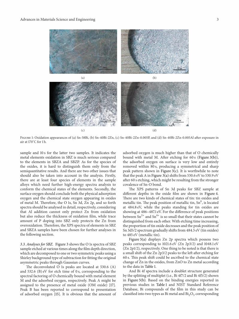
31 Observation of Liquid Solder Alloy Liquid Sn-58Bi alloyis easily oxidized in atmosphere condition The freshly dis-played surface remained silver-white for about 7min beforea gray white film formed Then the color of the liquid solder
alloy varies from gray blue with inhomogeneous purple andfinally dark blue with a light brownish yellow in some areaswithin 1 h (Figure 1(a)) In the same air exposure conditionZn-containing solder alloy SBZ loses metallic lustre afterabout 3min and keeps in white with a slight blue finally Thesolder surface is quite rough due to the Zn oxidation beforeduring and after cooling down as shown in Figure 1(b)
SBZP and SBZA solder alloys shine with grey or dark greymetallic lustre in liquid state within 1 h of exposure in airWith increasing oxidation time to about 30min an oxidationfilm with a slight grey white is visible on SBZP liquid surfacewhile the color on SBZA surface shows somewhat blueAfter cooling down to room temperature the surface growsrough on the surface of SBZP solder alloy (Figure 1(c)) Incomparison the metal surface of SBZA still keeps smooth insolid state as shown in Figure 1(d)
32 The Variation of Atomic Concentration with Etch TimeThe variation in chemical composition with etch time oftin oxygen bismuth zinc and aluminium or phosphorusobtained from the XPS survey scans for the three speci-mens (SBZ SBZA and SBZP) is shown in Figure 2 Theoxygen content on the outer surface among three specimensdecreases by the turn of SBZ SBZP to SBZA from about70 at to 60 at and then 45 at (see Figure 2(a)) It indi-cates that the oxidation film of SBZ is much porous More-over the total thicknesses of the oxide films after oxidationat 170∘C for 7min are about 156 nm for SBZA sample and216 nm for SBZ and SBZP alloys deduced from oxygencontent
As observed in Figures 2(b) and 2(c) for tin and bismuthas the main elements their concentrations increase with etchtime as expectedThe concentrations of zinc aluminium andphosphorus oppositely follow an increase sharply and thendecrease towards the solder base direction Among the threealloys it is worth noting that the Zn concentration on the topof the oxidation filmdecrease followed by SBZ SBZP to SBZAin turn corresponding to 404 at 369 at and 246 atrespectively It indicates that a trace amount of AlP dopingin SBZ solder can protect Zn from overoxidation as shown inFigures 2(d) and 2(e) Furthermore Zn is somewhat enrichedat the area of near surface also the outer surface comparedto the base-alloy composition Accordingly the contents ofAl and P are thousand times more than additive amountwhich suggests that the two elements have strong surfaceenrichment behavior in liquid solder alloy Thus there arethree peaks showing Zn Al and P at low etching time It canbe ascribed to the following three points First element Oespecially the absorbed oxidation makes the other elementcontents keep lower relatively second the chemical O keepsdriving Zn and AlP diffusion from the solder base to reactinto compounds finally the competition between the abovetwo reasons may result in the highest contents emerging atthe sublayer of the oxidation films
The ratios of metal elementM (M could be metal elementin samples) and oxygen on the surface are about 3 7 4 6and 45 55 for SBZ SBZP and SBZA respectively increasingrapidly to 6 4 after etching for 40 s with argon ions for SBZ
Advances in Materials Science and Engineering 3
(a) (b)
(c) (d)
Figure 1 Oxidation appearances of (a) Sn-58Bi (b) Sn-40Bi-2Zn (c) Sn-40Bi-2Zn-0005P and (d) Sn-40Bi-2Zn-0005Al after exposure inair at 170∘C for 1 h
sample and 10 s for the latter two samples It indicates themetal elements oxidation in SBZ is much serious comparedto the elements in SBZA and SBZP As for the species ofthe oxides it is hard to distinguish them only from thesemiquantitative results And there are two other issues thatshould also be taken into account in the analysis Firstlythere are at least four species of elements in the samplealloys which need further high-energy spectra analysis toconform the chemical states of the elements Secondly thesurface oxygen should conclude both the physical adsorptionoxygen and the chemical state oxygen appearing in oxidesof metal M Therefore the O 1s Sn 3d Zn 2p and so forthspectra should be analysed in detail respectively consideringthat Al addition cannot only protect Zn from oxidationbut also reduce the thickness of oxidation film while traceamount of P doping into SBZ only protects the Zn fromoveroxidationTherefore the XPS spectra of elements in SBZand SBZA samples have been chosen for further analyses inthe following section
33 Analyses for SBZ Figure 3 shows the O 1s spectra of SBZsample etched at various times along the film depth directionwhich are decomposed to one or two symmetric peaks using aShirley background type of subtraction for fitting the originalasymmetric peaks through Gaussian curves
The deconvoluted O 1s peaks are located at 5306 (A)and 5326 (B) eV for etch time of 0 s corresponding to thespectral factoring of O chemically bound with metal elementM and the adsorbed oxygen respectively Peak A might beassigned to the presence of metal oxide (OM oxide) [17]Peak B has been reported to correspond to presentationof adsorbed oxygen [15] It is obvious that the amount of
adsorbed oxygen is much higher than that of O chemicallybound with metal M After etching for 60 s (Figure 3(b))the adsorbed oxygen on surface is very low and entirelyremoved within 80 s producing a symmetrical and sharppeak pattern shown in Figure 3(c) It is worthwhile to notethat the peak A in Figure 3(a) shifts from 5306 eV to 5309 eVafter 60 s etching whichmight be resulting from the strongercovalence of Sn-O bond
The XPS patterns of Sn 3d peaks for SBZ sample atdifferent depths in the oxide film are shown in Figure 4There are two kinds of chemical states of tin tin oxides andmetallic tin The peak position of metallic tin Sn0 is locatedat 4848 eV while the peaks standing for tin oxides areshowing at 486ndash4871 eV For the difference of peak positionsbetween Sn2+ and Sn4+ is so small that their states cannot bedistinguished from each other With etching time increasingthe proportion of tin oxide decreases and the peak position ofSn 3d52 spectrum gradually shifts from 4845 eV (tin oxides)to 485 eV (metallic tin)
Figure 5(a) displays Zn 2p spectra which possess twopeaks corresponding to 10216 eV (Zn 2p32) and 10481 eV(Zn 2p12) respectively One thing to be noted is that there isa small shift of the Zn 2p32 peaks to the left after etching for60 s This peak shift could be ascribed to the chemical statechange of Zn in the oxides from ZnO to Zn metal accordingto the data in Table 1
And Bi 4f spectra include a doublet structure generatedby the splitting of multiplet (ie Bi 4f72 and Bi 4f52) shownin Figure 5(b) Based on the binding energies reported inprevious studies in Table 1 and NIST Standard ReferenceDatabase Bi compounds of the film in this study can beclassified into two types as Bi metal and Bi
2O3corresponding
4 Advances in Materials Science and Engineering
0 100 200 300 400 500 600
0
10
20
30
40
50
60
70
80
O 1s
SBZP
SBZA
SBZ
Atom
ic (
)
Etch time (s)
minus10
(a)
Atom
ic (
)
Etch time (s)0 100 200 300 400 500 600
0
5
10
15
20
25
30
Bi 4f
SBZPSBZA
SBZ
(b)
Atom
ic (
)
Etch time (s)0 100 200 300 400 500 600
0
10
20
30
40
50
60
70
Sn 3d
SBZP
SBZA
SBZ
(c)
Atom
ic (
)
Etch time (s)0 100 200 300 400 500 600
05
1015202530354045505560
Zn 2p
SBZP
SBZA
SBZ
(d)
Atom
ic (
)
Etch time (s)0 100 200 300 400 500 600
0
5
10
15
20
P 2p
Al 2p
(e)
Figure 2 XPS depth profiles (at) for (a) oxygen (b) zinc (c) tin (d) bismuth and (e) aluminium and phosphorus recorded for the SBZSBZA and SBZP specimens
Advances in Materials Science and Engineering 5
525 530 535 540 545
Original surface5326
5306
Inte
nsity
(au
)
Binding energy (eV)
A
B+
+
(a)
525 530 535 540 545
5328
5309
Inte
nsity
(au
)
Binding energy (eV)
+
+
Sputtering 60 s
(b)
Inte
nsity
(au
)
Binding energy (eV)525 530 535 540 545
5319Sputtering 80 s
(c)
Inte
nsity
(au
)
Binding energy (eV)525 530 535 540 545
Sputtering 260 s
(d)
Figure 3 O 1s spectra of SBZ sample exposure at 170∘C for 7min after etching for (a) 0 s (initial surface) (b) 10 s (c) 80 s and (d) 260 s
Table 1 XPS binding energy values for solder elements and the oxidative products obtained from literatures (Al O data fromNIST StandardReference Database 20 V 35)
Sn 3d52 (eV) Zn 2p32 (eV) Bi 4f72 (eV) Al 2p (eV) O 1sSn [15] 4848 mdashSnO [15 19] 4866486 mdash 5301SnO2 [15 19] 48644871 5310Zn [20] 102145ZnO [20] 10217 5307Bi [10] 1568Bi2O3 [10 17] 1595 5298Al [21] 73Al2O3 [18] 76-77 5326O [15] 5325
to the peak binding energies around 157 eV and 158 eVrespectively [10 17]
34 Analyses for SBZA The O 1s spectra of SBZA samplealong the depth of the oxide film are shown in Figure 6 ThedeconvolutedO 1s peaks for original surface are located at 531(A1015840) eV and 5326 (B1015840) eV Based on the results in Figure 3 A1015840
peak can be assigned to metal oxide (OM oxygen) and thelatter B1015840may relate to the adsorbed oxygen like SBZ alloy andthe emerging Al
2O3[18] However B1015840 peak disappears after
20 s of etching It should be the absorbed oxygen mainly Thebinding energy of peak A1015840 is 04 eV higher than the positionof peak A in SBZ sample which may indicate the specieschanges of oxides in the outmost surface of the film
6 Advances in Materials Science and Engineering
475 480 485 490 495 500
Inte
nsity
(au
)
Binding energy (eV)
(a)
Inte
nsity
(au
)
Binding energy (eV)480 482 484 486 488 490
4845
4864
Sputtering 60 s
(b)
Inte
nsity
(au
)
Binding energy (eV)480 482 484 486 488 490
48501
4846
120 s
(c)
Inte
nsity
(au
)
Binding energy (eV)480 482 484 486 488 490
4863
48501
240 s
(d)
Figure 4 Sn 3d52 spectra of SBZ sample exposure at 170∘C for 7min after etching for (a) 0 s (initial surface) (b) 10 s (c) 140 s and (d) 260 s
1010 1015 1020 1025 1030 1035 1040 1045 1050 1055
10217
Inte
nsity
(au
)
Binding energy (eV)
10481 eV10216 eV
180 s
120 s
60 s
0 s
(a)
Inte
nsity
(au
)
Binding energy (eV)154 156 158 160 162 164 166 168
+157 eV
1581 eV
120 s
60 s0 s
+
(b)
Figure 5 Spectra of (a) Zn 2p and (b) Bi 4f in SBZ sample oxidized at 170∘C for 7min after etching for various time
Advances in Materials Science and Engineering 7
526 528 530 532 534 536 538
Original surface
5315326
Inte
nsity
(au
)
Binding energy (eV)
A998400
B 998400
++
(a)
Inte
nsity
(au
)
Binding energy (eV)525 530 535 540 545
531 5326
Sputtering 10 s
++
(b)
Inte
nsity
(au
)
Binding energy (eV)525 530 535 540 545
5315Sputtering 20 s
(c)
Inte
nsity
(au
)
Binding energy (eV)525 530 535 540 545
5317
Sputtering 80 s
(d)
Figure 6 O 1s spectra of SBZA sample exposure at 170∘C for 7min after etching for (a) 0 s (initial surface) (b) 10 s (c) 20 s and (d) 80 s
According to the atomic concentration depth profile ofSBZA etched for 0 s it is found that there are mainly Zn andAl in the outer surface of the oxidation film And consideringthat O chemically bounded with Zn located at 5307 eV Obounded with Al located at 5326 eV the OM oxygen shouldbemainly ZnOandAl
2O3with a little Bi and Sn inside PeakB
which corresponded to adsorbed oxygen (5325 eV) [17] andAl2O3[19] that could not be resolved becomes lower and
totally disappears after etching for 20 s That is the film ofSBZA sample is much denser than the surface film of SBZsample because the time getting to zero for physical adsorbedoxygen in SBZ sample requires 60 s 40 s more than SBZAsample
It is noteworthy that peak A1015840 shifts from 531 eV to higherbinding energy 5315 eV after 20 s etch time then 5317 eV atthe etching time of 80 s which might be also ascribed to thestronger Sn-O bond similar to the SBZ sample
Sn 3d spectra along the film depth are shown in Figure 7Similar to the results for SBZ in Figure 3 the peak positionof Sn 3d52 of the original outer surface is positioned at48703 eV However after 80 s of etching Sn 3d peak shifts
slightly to 48631 eV first and then maintains its position tillthe tin oxide disappears Both the binding energy of the outersurface and the subsurface are slightly greater than that ofthe SBZ oxide film The possible reason may lie in a strongelectron withdrawing group or compounds around the tinatoms which changed the chemical conditions resulting bythe trace amount of Al addition After removing 36 nm fromthe surface by etching no oxide has been detected by XPSThe peak position of metallic tin is located at 48486 eV asshown in Figure 7(d)
Figure 8 shows the XPS spectra of Al 2p depth profiles ofoxide film in SBZA sample The XPS peak height (Al contentcan be estimated) on the subsurface of oxidation is higherthan that on the outer surfaceThe detected segregation layerof Al is very thin distributed over a depth of about 12ndash48 nmfrom the outer surface There is no visible Al peak detectedbeyond the area From Figure 8 it is found that an almostinvisible peak around 751 eV is showing at the outer filmsurface After etching for 20 s a new peak located at 722 eVarises corresponding to metal Al It implies the enrichmentbehavior of element Al at the subsurface that the atom Al
8 Advances in Materials Science and Engineering
480 482 484 486 488 490
Original surface 48703
48492
Inte
nsity
(au
)
Binding energy (eV)
(a)
Inte
nsity
(au
)
Binding energy (eV)480 482 484 486 488 490
48491
48689
Sputtering 10 s
(b)
Inte
nsity
(au
)
Binding energy (eV)480 482 484 486 488 490
48648
48486Sputtering 20 s
(c)
Inte
nsity
(au
)
Binding energy (eV)480 482 484 486 488 490
48631
48487Sputtering 80 s
(d)
Inte
nsity
(au
)
Binding energy (eV)478 480 482 484 486 488 490
48486
48627
Sputtering 140 s
(e)
Inte
nsity
(au
)
Binding energy (eV)480 482 484 486 488 490
48486
4864
Sputtering 260 s
(f)
Figure 7 Sn 3d52 spectra of SBZA sample exposure at 170∘C for 7min after etching for (a) 0 s (initial surface) (b) 10 s (c) 20 s (d) 80 s(e) 140 s and (f) 260 s
Advances in Materials Science and Engineering 9
65 70 75 80 85
Inte
nsity
(au
)
Binding energy (eV)
746 eV140 s
80 s
20 s
10 s0 s
(a)
Inte
nsity
(au
)
Binding energy (eV)65 70 75 80 85
Original surface sputtering 0 s
(b)
Inte
nsity
(au
)
Binding energy (eV)70 72 74 76 78 80
7219
746 eV
Sputtering 20 s
+
+
(c)
Inte
nsity
(au
)
Binding energy (eV)72 73 74 75 76 77
737 eV
751 eV
Sputtering 80 s
+
+
(d)
Figure 8 Al 2p spectra of SBZA sample exposure at 170∘C for 7min after etching for (a) various times from 0 s to 140 s (b) 0 s (initial surface)(c) 20 s and (d) 80 s
can be kept as a lower chemical state Al0 While the etchingtime increases to 80 s both kinds of peaks shift to higherenergy direction It suggests that there is a new chemicalstate of Al in the oxide Based on [18] this peak position forAl 2p approaches that of Al
2O3 with 09sim19 eV deviation
which might result by Sn and Bi dissolved in the oxidationfilm However further research is necessary to clarify the Almechanism in the protective oxide film
Combined with the result of semiquantitative analysis(see Figure 2) it is reasonable to propose that there is atriple-layer oxidation film structureThe outer surface shouldmainly comprise of O in physical status and ZnO with about6 nm in thickness The subsurface should be ZnO and Al
2O3
doped with Sn4+ and Bi3+ to about 30ndash84 nm thicknessaccording to Al element getting to almost zero and Sn metalcontents almost being the main in all forms of Sn whichcould be a protective film to prevent further oxidation of themolten solder alloy in atmosphere condition And the innerremaining thickness of the film layer should be (Sn Bi andZn) O as a transition layer
4 Conclusion
The properties of the oxide film that forms on liquid SBZsolder and the effect of AlP addition on the film propertieswere investigated by XPS depth profiling at 170∘C for 7min
(1) It was found that the thickness of the SBZ oxide wasapproximately 216 nm Further XPS analysis revealedthat the oxide film close to the substrate mainlycomposed of Sn2+ oxides which consisted mostly ofZn2+ oxides near the free surfaceThe amount of Sn4+and Bi3+ oxides generated near the film surface wasfound to be similar to the three types of samples
(2) With 0005wt Al addition to SBZ creating a SBZAalloy a triple-layer oxidation film structure can beobserved The outer surface should mainly compriseof physical absorbed O and ZnO Oxides of Zn andAl are mainly responsible for the formation of thesubsurface of SBZA alloy The oxides of Sn and Biforming the innermost layer also contribute a little
10 Advances in Materials Science and Engineering
to the film formation Considerable Al segregationoccurs towards the surface principally as Al
2O3
(3) A trace amount of P doped to SBZ could not decreasethe thickness of the oxidation film But the Zn contentin the outer surface of oxidation was decreased Thissupports the idea that a minus P can protect Zn fromexcess oxidation
(4) This work suggests that the solders with Zn can beconsidered as a potential alternative with traceamount of Al addition for low melting point soldersespecially when the oxidation of the liquid solder is aconcern
Conflict of Interests
The authors declare that there is no conflict of interestsregarding the publication of this paper
Acknowledgments
The authors would like to thank Senior Engineer G L Gongin Nokia Corporation and Professor C Yan in Jiangsu Uni-versity of Science and Technology for the useful discussionon XPS data analysis They also express their appreciation toP Y Guo for editorial revising This work was supported bythe National Natural Science Fund (51201072)
References
[1] X C Tong ldquoThermal interface materials in electronic pack-agingrdquo in Advanced Materials for Thermal Management ofElectronic Packaging vol 30 of Springer Series in AdvancedMicroelectronics pp 305ndash371 Springer Berlin Germany 2011
[2] L Zang Z Yuan Y Zhu B Xu HMatsuura and F TsukihashildquoSpreading process and interfacial characteristic of Sn-17Bi-05CuNi at temperatures ranging from 523K to 673Krdquo Colloidsand Surfaces A Physicochemical and Engineering Aspects vol414 pp 57ndash65 2012
[3] G FMa H L Zhang H F Zhang H Li and Z QHu ldquoInterfa-cial characteristics of molten Bi-43Sn alloy on amorphous andcrystalline Fe
78B13Si9rdquo Materials Letters vol 62 no 12-13 pp
1853ndash1855 2008[4] H He H Zhao F Guo and G Xu ldquoBi layer formation at
the anode interface in CuSn-58BiCu solder joints with highcurrent densityrdquo Journal of Materials Science amp Technology vol28 no 1 pp 46ndash52 2012
[5] X J Wang Y L Wang F J Wang N Liu and J X WangldquoEffects of Zn Zn-Al and Zn-P additions on the tensileproperties of Sn-Bi solderrdquo Acta Metallurgica Sinica vol 27 no6 pp 1159ndash1164 2014
[6] A A El-Daly and A M El-Taher ldquoImproved strength of Niand Zn-doped Snndash20Agndash05Cu lead-free solder alloys undercontrolled processing parametersrdquo Materials amp Design vol 47pp 607ndash614 2013
[7] Y M Kim T J Kim M Y Choi and Y-H Kim ldquoInterfacialreactions between Sn-30Ag-05Cu solder and Cu-xZn (x = 0ndash35 wt) or Cu-xZn-yNi (x = 20 and 25 wt y = 15 and 10 wt)substratesrdquo Journal of Alloys and Compounds vol 575 pp 350ndash358 2013
[8] H J Lin and T H Chuang ldquoEffects of Ce and Zn additionson the microstructure and mechanical properties of Snndash3Agndash05Cu solder jointsrdquo Journal of Alloys and Compounds vol 500no 2 pp 167ndash174 2010
[9] T-C Chang J-W Wang M-C Wang and M-H HonldquoSolderability of Sn-9Zn-05Ag-1In lead-free solder on Cusubstrate part 1Thermal properties microstructure corrosionand oxidation resistancerdquo Journal of Alloys and Compounds vol422 no 1-2 pp 239ndash243 2006
[10] K-L Lin and T-P Liu ldquoHigh-temperature oxidation of a Sn-Zn-Al solderrdquoOxidation of Metals vol 50 no 3-4 pp 255ndash2671998
[11] M L Huang N Kang Q Zhou and Y Z Huang ldquoEffect ofNi content on mechanical properties and corrosion behaviorof AlSnndash9ZnndashxNiCu jointsrdquo Journal of Materials Science ampTechnology vol 28 no 9 pp 844ndash852 2012
[12] L Zhang S B Xue L L Gao et al ldquoDevelopment of Sn-Zn lead-free solders bearing alloying elementsrdquo Journal ofMaterials Science Materials in Electronics vol 21 no 1 pp 1ndash15 2010
[13] P Ghodsa O B Isgora J R Brownb F Bensebaac and DKingstonc ldquoXPS depth profiling study on the passive oxide filmof carbon steel in saturated calcium hydroxide solution andthe effect of chloride on the film propertiesrdquo Applied SurfaceScience vol 257 no 10 pp 4669ndash4677 2011
[14] J Mittal Y W Lin and K L Lin ldquoInfluence of Cu substratesurface oxides and heating rates during reflow onmelting pointof Sn-35Ag solderrdquo Applied Surface Science vol 256 no 11 pp3531ndash3540 2010
[15] A-P Xian and G-L Gong ldquoSurface oxidation of molten Snndash007 wt P in air at 280 ∘Crdquo Journal of Materials Research vol23 no 6 pp 1532ndash1536 2008
[16] D Briggs andM P Seah Practical Surface Analysis Wiley NewYork NY USA 1983
[17] J-M Song Y-M Cheng and C-H Tsai ldquoOxidation of liquidsolders for die attachmentrdquoCorrosion Science vol 52 no 12 pp4011ndash4016 2010
[18] U SMohanty andK L Lin ldquoEffect of Al on the electrochemicalcorrosion behaviour of Pb free Snndash85 Znndash05 AgndashXAlndash05 Gasolder in 35 NaCl solutionrdquo Applied Surface Science vol 252pp 5907ndash5916 2006
[19] G E Muilenberg Handbook of X-Ray Photoelectron Sec-troscopy Perkin-Elmer Eden Prairie Minn USA 1992
[20] J Chastain Handbook of X-Ray Photoelectron SectroscopyPerkinElmer Waltham Mass USA 1992
[21] A Nylund and I Olefjord ldquoSurface analysis of oxidized alu-minum 1 Hydration of Al
2O3and decomposition of Al(OH)
3
in a vacuum as studied by ESCArdquo Surface and Interface Analysisvol 21 no 5 pp 283ndash289 1994
Submit your manuscripts athttpwwwhindawicom
ScientificaHindawi Publishing Corporationhttpwwwhindawicom Volume 2014
CorrosionInternational Journal of
Hindawi Publishing Corporationhttpwwwhindawicom Volume 2014
Polymer ScienceInternational Journal of
Hindawi Publishing Corporationhttpwwwhindawicom Volume 2014
Hindawi Publishing Corporationhttpwwwhindawicom Volume 2014
CeramicsJournal of
Hindawi Publishing Corporationhttpwwwhindawicom Volume 2014
CompositesJournal of
NanoparticlesJournal of
Hindawi Publishing Corporationhttpwwwhindawicom Volume 2014
Hindawi Publishing Corporationhttpwwwhindawicom Volume 2014
International Journal of
Biomaterials
Hindawi Publishing Corporationhttpwwwhindawicom Volume 2014
NanoscienceJournal of
TextilesHindawi Publishing Corporation httpwwwhindawicom Volume 2014
Journal of
NanotechnologyHindawi Publishing Corporationhttpwwwhindawicom Volume 2014
Journal of
CrystallographyJournal of
Hindawi Publishing Corporationhttpwwwhindawicom Volume 2014
The Scientific World JournalHindawi Publishing Corporation httpwwwhindawicom Volume 2014
Hindawi Publishing Corporationhttpwwwhindawicom Volume 2014
CoatingsJournal of
Advances in
Materials Science and EngineeringHindawi Publishing Corporationhttpwwwhindawicom Volume 2014
Smart Materials Research
Hindawi Publishing Corporationhttpwwwhindawicom Volume 2014
Hindawi Publishing Corporationhttpwwwhindawicom Volume 2014
MetallurgyJournal of
Hindawi Publishing Corporationhttpwwwhindawicom Volume 2014
BioMed Research International
MaterialsJournal of
Hindawi Publishing Corporationhttpwwwhindawicom Volume 2014
Nano
materials
Hindawi Publishing Corporationhttpwwwhindawicom Volume 2014
Journal ofNanomaterials
2 Advances in Materials Science and Engineering
new [13 14] Many efforts focusing on oxide formation oniron steel and molten tin have been implemented [13ndash15]
2 Experimental Procedures
21 Preparation of Specimens SBZ SBZA SBZP and Sn-58Bialloys (for comparison in oxidation observation by eye) wereprepared using pure Sn Bi Zn Al and P in vacuum ovenat 800∘C and remelted with stirring at 200∘C to obtain ahomogenized solder alloy During the remelting process anantioxidation agent was used to protect the liquid solder fromoxidation Subsequently the solder alloys were aged for twoweeks in room temperature for a stabilized microstructure
22 Surface Observation of Solder Alloy after OxidationAbout 40 g solder alloys were put in graphite crucibles with adiameter of 28mm and heated up to 170 plusmn 5∘C to observe theoxidation processes during 1 h in air The first dross shouldbe carefully scraped away from the initial liquid surface toleave a fresh surface for oxidation starting therefrom Thecolor changes of the liquid solder surface with oxidation timeincreasing were observed visually and the final appearance ofthe oxide films was recorded by a digital camera
23 XPS Procedure Solder alloys were exposed at 170 plusmn 5∘Cfor 7min before cooling down to achieve oxidized surfacesThe solid samples were cut from the top surface of the ingotsinto about 2-3mm sheets for XPS tests For the test is sensitiveto pollution all the samples should be kept carefully awayfrom contaminations
The surface elementary and chemical analyses were car-ried out via XPS with an achromatic Al K
120572X-ray source
After the original surface of samples was analyzed an argonion beam with 02 120583A current operating at 3 keV was used toetch away a very thin layer of the solder from the oxidationsurface to expose the underlying layer Subsequently a secondsurface analysis of the newer oxide film was performed byXPS with an argon gun attached to So repeatedly an etchrate of about 06 nms was motivated over a 2mm times 2mmarea by the manner the same as [16]
24 XSP Data Analysis The etching and measurement foreach sample were operated about 10 times till the oxygencontent test on the surface becomes near to zero All thespectra were calibrated by carbon adsorbed on the initialsurface of the sample during etching
Curve fitting processes for all high-resolution spectrawere implemented by the XPS Peak-Fitting Programme-XPSPEAK41 to deconvolute and quantify the contributionof each chemical species (element associations) that comprisethe spectra
3 Results and Discussion
31 Observation of Liquid Solder Alloy Liquid Sn-58Bi alloyis easily oxidized in atmosphere condition The freshly dis-played surface remained silver-white for about 7min beforea gray white film formed Then the color of the liquid solder
alloy varies from gray blue with inhomogeneous purple andfinally dark blue with a light brownish yellow in some areaswithin 1 h (Figure 1(a)) In the same air exposure conditionZn-containing solder alloy SBZ loses metallic lustre afterabout 3min and keeps in white with a slight blue finally Thesolder surface is quite rough due to the Zn oxidation beforeduring and after cooling down as shown in Figure 1(b)
SBZP and SBZA solder alloys shine with grey or dark greymetallic lustre in liquid state within 1 h of exposure in airWith increasing oxidation time to about 30min an oxidationfilm with a slight grey white is visible on SBZP liquid surfacewhile the color on SBZA surface shows somewhat blueAfter cooling down to room temperature the surface growsrough on the surface of SBZP solder alloy (Figure 1(c)) Incomparison the metal surface of SBZA still keeps smooth insolid state as shown in Figure 1(d)
32 The Variation of Atomic Concentration with Etch TimeThe variation in chemical composition with etch time oftin oxygen bismuth zinc and aluminium or phosphorusobtained from the XPS survey scans for the three speci-mens (SBZ SBZA and SBZP) is shown in Figure 2 Theoxygen content on the outer surface among three specimensdecreases by the turn of SBZ SBZP to SBZA from about70 at to 60 at and then 45 at (see Figure 2(a)) It indi-cates that the oxidation film of SBZ is much porous More-over the total thicknesses of the oxide films after oxidationat 170∘C for 7min are about 156 nm for SBZA sample and216 nm for SBZ and SBZP alloys deduced from oxygencontent
As observed in Figures 2(b) and 2(c) for tin and bismuthas the main elements their concentrations increase with etchtime as expectedThe concentrations of zinc aluminium andphosphorus oppositely follow an increase sharply and thendecrease towards the solder base direction Among the threealloys it is worth noting that the Zn concentration on the topof the oxidation filmdecrease followed by SBZ SBZP to SBZAin turn corresponding to 404 at 369 at and 246 atrespectively It indicates that a trace amount of AlP dopingin SBZ solder can protect Zn from overoxidation as shown inFigures 2(d) and 2(e) Furthermore Zn is somewhat enrichedat the area of near surface also the outer surface comparedto the base-alloy composition Accordingly the contents ofAl and P are thousand times more than additive amountwhich suggests that the two elements have strong surfaceenrichment behavior in liquid solder alloy Thus there arethree peaks showing Zn Al and P at low etching time It canbe ascribed to the following three points First element Oespecially the absorbed oxidation makes the other elementcontents keep lower relatively second the chemical O keepsdriving Zn and AlP diffusion from the solder base to reactinto compounds finally the competition between the abovetwo reasons may result in the highest contents emerging atthe sublayer of the oxidation films
The ratios of metal elementM (M could be metal elementin samples) and oxygen on the surface are about 3 7 4 6and 45 55 for SBZ SBZP and SBZA respectively increasingrapidly to 6 4 after etching for 40 s with argon ions for SBZ
Advances in Materials Science and Engineering 3
(a) (b)
(c) (d)
Figure 1 Oxidation appearances of (a) Sn-58Bi (b) Sn-40Bi-2Zn (c) Sn-40Bi-2Zn-0005P and (d) Sn-40Bi-2Zn-0005Al after exposure inair at 170∘C for 1 h
sample and 10 s for the latter two samples It indicates themetal elements oxidation in SBZ is much serious comparedto the elements in SBZA and SBZP As for the species ofthe oxides it is hard to distinguish them only from thesemiquantitative results And there are two other issues thatshould also be taken into account in the analysis Firstlythere are at least four species of elements in the samplealloys which need further high-energy spectra analysis toconform the chemical states of the elements Secondly thesurface oxygen should conclude both the physical adsorptionoxygen and the chemical state oxygen appearing in oxidesof metal M Therefore the O 1s Sn 3d Zn 2p and so forthspectra should be analysed in detail respectively consideringthat Al addition cannot only protect Zn from oxidationbut also reduce the thickness of oxidation film while traceamount of P doping into SBZ only protects the Zn fromoveroxidationTherefore the XPS spectra of elements in SBZand SBZA samples have been chosen for further analyses inthe following section
33 Analyses for SBZ Figure 3 shows the O 1s spectra of SBZsample etched at various times along the film depth directionwhich are decomposed to one or two symmetric peaks using aShirley background type of subtraction for fitting the originalasymmetric peaks through Gaussian curves
The deconvoluted O 1s peaks are located at 5306 (A)and 5326 (B) eV for etch time of 0 s corresponding to thespectral factoring of O chemically bound with metal elementM and the adsorbed oxygen respectively Peak A might beassigned to the presence of metal oxide (OM oxide) [17]Peak B has been reported to correspond to presentationof adsorbed oxygen [15] It is obvious that the amount of
adsorbed oxygen is much higher than that of O chemicallybound with metal M After etching for 60 s (Figure 3(b))the adsorbed oxygen on surface is very low and entirelyremoved within 80 s producing a symmetrical and sharppeak pattern shown in Figure 3(c) It is worthwhile to notethat the peak A in Figure 3(a) shifts from 5306 eV to 5309 eVafter 60 s etching whichmight be resulting from the strongercovalence of Sn-O bond
The XPS patterns of Sn 3d peaks for SBZ sample atdifferent depths in the oxide film are shown in Figure 4There are two kinds of chemical states of tin tin oxides andmetallic tin The peak position of metallic tin Sn0 is locatedat 4848 eV while the peaks standing for tin oxides areshowing at 486ndash4871 eV For the difference of peak positionsbetween Sn2+ and Sn4+ is so small that their states cannot bedistinguished from each other With etching time increasingthe proportion of tin oxide decreases and the peak position ofSn 3d52 spectrum gradually shifts from 4845 eV (tin oxides)to 485 eV (metallic tin)
Figure 5(a) displays Zn 2p spectra which possess twopeaks corresponding to 10216 eV (Zn 2p32) and 10481 eV(Zn 2p12) respectively One thing to be noted is that there isa small shift of the Zn 2p32 peaks to the left after etching for60 s This peak shift could be ascribed to the chemical statechange of Zn in the oxides from ZnO to Zn metal accordingto the data in Table 1
And Bi 4f spectra include a doublet structure generatedby the splitting of multiplet (ie Bi 4f72 and Bi 4f52) shownin Figure 5(b) Based on the binding energies reported inprevious studies in Table 1 and NIST Standard ReferenceDatabase Bi compounds of the film in this study can beclassified into two types as Bi metal and Bi
2O3corresponding
4 Advances in Materials Science and Engineering
0 100 200 300 400 500 600
0
10
20
30
40
50
60
70
80
O 1s
SBZP
SBZA
SBZ
Atom
ic (
)
Etch time (s)
minus10
(a)
Atom
ic (
)
Etch time (s)0 100 200 300 400 500 600
0
5
10
15
20
25
30
Bi 4f
SBZPSBZA
SBZ
(b)
Atom
ic (
)
Etch time (s)0 100 200 300 400 500 600
0
10
20
30
40
50
60
70
Sn 3d
SBZP
SBZA
SBZ
(c)
Atom
ic (
)
Etch time (s)0 100 200 300 400 500 600
05
1015202530354045505560
Zn 2p
SBZP
SBZA
SBZ
(d)
Atom
ic (
)
Etch time (s)0 100 200 300 400 500 600
0
5
10
15
20
P 2p
Al 2p
(e)
Figure 2 XPS depth profiles (at) for (a) oxygen (b) zinc (c) tin (d) bismuth and (e) aluminium and phosphorus recorded for the SBZSBZA and SBZP specimens
Advances in Materials Science and Engineering 5
525 530 535 540 545
Original surface5326
5306
Inte
nsity
(au
)
Binding energy (eV)
A
B+
+
(a)
525 530 535 540 545
5328
5309
Inte
nsity
(au
)
Binding energy (eV)
+
+
Sputtering 60 s
(b)
Inte
nsity
(au
)
Binding energy (eV)525 530 535 540 545
5319Sputtering 80 s
(c)
Inte
nsity
(au
)
Binding energy (eV)525 530 535 540 545
Sputtering 260 s
(d)
Figure 3 O 1s spectra of SBZ sample exposure at 170∘C for 7min after etching for (a) 0 s (initial surface) (b) 10 s (c) 80 s and (d) 260 s
Table 1 XPS binding energy values for solder elements and the oxidative products obtained from literatures (Al O data fromNIST StandardReference Database 20 V 35)
Sn 3d52 (eV) Zn 2p32 (eV) Bi 4f72 (eV) Al 2p (eV) O 1sSn [15] 4848 mdashSnO [15 19] 4866486 mdash 5301SnO2 [15 19] 48644871 5310Zn [20] 102145ZnO [20] 10217 5307Bi [10] 1568Bi2O3 [10 17] 1595 5298Al [21] 73Al2O3 [18] 76-77 5326O [15] 5325
to the peak binding energies around 157 eV and 158 eVrespectively [10 17]
34 Analyses for SBZA The O 1s spectra of SBZA samplealong the depth of the oxide film are shown in Figure 6 ThedeconvolutedO 1s peaks for original surface are located at 531(A1015840) eV and 5326 (B1015840) eV Based on the results in Figure 3 A1015840
peak can be assigned to metal oxide (OM oxygen) and thelatter B1015840may relate to the adsorbed oxygen like SBZ alloy andthe emerging Al
2O3[18] However B1015840 peak disappears after
20 s of etching It should be the absorbed oxygen mainly Thebinding energy of peak A1015840 is 04 eV higher than the positionof peak A in SBZ sample which may indicate the specieschanges of oxides in the outmost surface of the film
6 Advances in Materials Science and Engineering
475 480 485 490 495 500
Inte
nsity
(au
)
Binding energy (eV)
(a)
Inte
nsity
(au
)
Binding energy (eV)480 482 484 486 488 490
4845
4864
Sputtering 60 s
(b)
Inte
nsity
(au
)
Binding energy (eV)480 482 484 486 488 490
48501
4846
120 s
(c)
Inte
nsity
(au
)
Binding energy (eV)480 482 484 486 488 490
4863
48501
240 s
(d)
Figure 4 Sn 3d52 spectra of SBZ sample exposure at 170∘C for 7min after etching for (a) 0 s (initial surface) (b) 10 s (c) 140 s and (d) 260 s
1010 1015 1020 1025 1030 1035 1040 1045 1050 1055
10217
Inte
nsity
(au
)
Binding energy (eV)
10481 eV10216 eV
180 s
120 s
60 s
0 s
(a)
Inte
nsity
(au
)
Binding energy (eV)154 156 158 160 162 164 166 168
+157 eV
1581 eV
120 s
60 s0 s
+
(b)
Figure 5 Spectra of (a) Zn 2p and (b) Bi 4f in SBZ sample oxidized at 170∘C for 7min after etching for various time
Advances in Materials Science and Engineering 7
526 528 530 532 534 536 538
Original surface
5315326
Inte
nsity
(au
)
Binding energy (eV)
A998400
B 998400
++
(a)
Inte
nsity
(au
)
Binding energy (eV)525 530 535 540 545
531 5326
Sputtering 10 s
++
(b)
Inte
nsity
(au
)
Binding energy (eV)525 530 535 540 545
5315Sputtering 20 s
(c)
Inte
nsity
(au
)
Binding energy (eV)525 530 535 540 545
5317
Sputtering 80 s
(d)
Figure 6 O 1s spectra of SBZA sample exposure at 170∘C for 7min after etching for (a) 0 s (initial surface) (b) 10 s (c) 20 s and (d) 80 s
According to the atomic concentration depth profile ofSBZA etched for 0 s it is found that there are mainly Zn andAl in the outer surface of the oxidation film And consideringthat O chemically bounded with Zn located at 5307 eV Obounded with Al located at 5326 eV the OM oxygen shouldbemainly ZnOandAl
2O3with a little Bi and Sn inside PeakB
which corresponded to adsorbed oxygen (5325 eV) [17] andAl2O3[19] that could not be resolved becomes lower and
totally disappears after etching for 20 s That is the film ofSBZA sample is much denser than the surface film of SBZsample because the time getting to zero for physical adsorbedoxygen in SBZ sample requires 60 s 40 s more than SBZAsample
It is noteworthy that peak A1015840 shifts from 531 eV to higherbinding energy 5315 eV after 20 s etch time then 5317 eV atthe etching time of 80 s which might be also ascribed to thestronger Sn-O bond similar to the SBZ sample
Sn 3d spectra along the film depth are shown in Figure 7Similar to the results for SBZ in Figure 3 the peak positionof Sn 3d52 of the original outer surface is positioned at48703 eV However after 80 s of etching Sn 3d peak shifts
slightly to 48631 eV first and then maintains its position tillthe tin oxide disappears Both the binding energy of the outersurface and the subsurface are slightly greater than that ofthe SBZ oxide film The possible reason may lie in a strongelectron withdrawing group or compounds around the tinatoms which changed the chemical conditions resulting bythe trace amount of Al addition After removing 36 nm fromthe surface by etching no oxide has been detected by XPSThe peak position of metallic tin is located at 48486 eV asshown in Figure 7(d)
Figure 8 shows the XPS spectra of Al 2p depth profiles ofoxide film in SBZA sample The XPS peak height (Al contentcan be estimated) on the subsurface of oxidation is higherthan that on the outer surfaceThe detected segregation layerof Al is very thin distributed over a depth of about 12ndash48 nmfrom the outer surface There is no visible Al peak detectedbeyond the area From Figure 8 it is found that an almostinvisible peak around 751 eV is showing at the outer filmsurface After etching for 20 s a new peak located at 722 eVarises corresponding to metal Al It implies the enrichmentbehavior of element Al at the subsurface that the atom Al
8 Advances in Materials Science and Engineering
480 482 484 486 488 490
Original surface 48703
48492
Inte
nsity
(au
)
Binding energy (eV)
(a)
Inte
nsity
(au
)
Binding energy (eV)480 482 484 486 488 490
48491
48689
Sputtering 10 s
(b)
Inte
nsity
(au
)
Binding energy (eV)480 482 484 486 488 490
48648
48486Sputtering 20 s
(c)
Inte
nsity
(au
)
Binding energy (eV)480 482 484 486 488 490
48631
48487Sputtering 80 s
(d)
Inte
nsity
(au
)
Binding energy (eV)478 480 482 484 486 488 490
48486
48627
Sputtering 140 s
(e)
Inte
nsity
(au
)
Binding energy (eV)480 482 484 486 488 490
48486
4864
Sputtering 260 s
(f)
Figure 7 Sn 3d52 spectra of SBZA sample exposure at 170∘C for 7min after etching for (a) 0 s (initial surface) (b) 10 s (c) 20 s (d) 80 s(e) 140 s and (f) 260 s
Advances in Materials Science and Engineering 9
65 70 75 80 85
Inte
nsity
(au
)
Binding energy (eV)
746 eV140 s
80 s
20 s
10 s0 s
(a)
Inte
nsity
(au
)
Binding energy (eV)65 70 75 80 85
Original surface sputtering 0 s
(b)
Inte
nsity
(au
)
Binding energy (eV)70 72 74 76 78 80
7219
746 eV
Sputtering 20 s
+
+
(c)
Inte
nsity
(au
)
Binding energy (eV)72 73 74 75 76 77
737 eV
751 eV
Sputtering 80 s
+
+
(d)
Figure 8 Al 2p spectra of SBZA sample exposure at 170∘C for 7min after etching for (a) various times from 0 s to 140 s (b) 0 s (initial surface)(c) 20 s and (d) 80 s
can be kept as a lower chemical state Al0 While the etchingtime increases to 80 s both kinds of peaks shift to higherenergy direction It suggests that there is a new chemicalstate of Al in the oxide Based on [18] this peak position forAl 2p approaches that of Al
2O3 with 09sim19 eV deviation
which might result by Sn and Bi dissolved in the oxidationfilm However further research is necessary to clarify the Almechanism in the protective oxide film
Combined with the result of semiquantitative analysis(see Figure 2) it is reasonable to propose that there is atriple-layer oxidation film structureThe outer surface shouldmainly comprise of O in physical status and ZnO with about6 nm in thickness The subsurface should be ZnO and Al
2O3
doped with Sn4+ and Bi3+ to about 30ndash84 nm thicknessaccording to Al element getting to almost zero and Sn metalcontents almost being the main in all forms of Sn whichcould be a protective film to prevent further oxidation of themolten solder alloy in atmosphere condition And the innerremaining thickness of the film layer should be (Sn Bi andZn) O as a transition layer
4 Conclusion
The properties of the oxide film that forms on liquid SBZsolder and the effect of AlP addition on the film propertieswere investigated by XPS depth profiling at 170∘C for 7min
(1) It was found that the thickness of the SBZ oxide wasapproximately 216 nm Further XPS analysis revealedthat the oxide film close to the substrate mainlycomposed of Sn2+ oxides which consisted mostly ofZn2+ oxides near the free surfaceThe amount of Sn4+and Bi3+ oxides generated near the film surface wasfound to be similar to the three types of samples
(2) With 0005wt Al addition to SBZ creating a SBZAalloy a triple-layer oxidation film structure can beobserved The outer surface should mainly compriseof physical absorbed O and ZnO Oxides of Zn andAl are mainly responsible for the formation of thesubsurface of SBZA alloy The oxides of Sn and Biforming the innermost layer also contribute a little
10 Advances in Materials Science and Engineering
to the film formation Considerable Al segregationoccurs towards the surface principally as Al
2O3
(3) A trace amount of P doped to SBZ could not decreasethe thickness of the oxidation film But the Zn contentin the outer surface of oxidation was decreased Thissupports the idea that a minus P can protect Zn fromexcess oxidation
(4) This work suggests that the solders with Zn can beconsidered as a potential alternative with traceamount of Al addition for low melting point soldersespecially when the oxidation of the liquid solder is aconcern
Conflict of Interests
The authors declare that there is no conflict of interestsregarding the publication of this paper
Acknowledgments
The authors would like to thank Senior Engineer G L Gongin Nokia Corporation and Professor C Yan in Jiangsu Uni-versity of Science and Technology for the useful discussionon XPS data analysis They also express their appreciation toP Y Guo for editorial revising This work was supported bythe National Natural Science Fund (51201072)
References
[1] X C Tong ldquoThermal interface materials in electronic pack-agingrdquo in Advanced Materials for Thermal Management ofElectronic Packaging vol 30 of Springer Series in AdvancedMicroelectronics pp 305ndash371 Springer Berlin Germany 2011
[2] L Zang Z Yuan Y Zhu B Xu HMatsuura and F TsukihashildquoSpreading process and interfacial characteristic of Sn-17Bi-05CuNi at temperatures ranging from 523K to 673Krdquo Colloidsand Surfaces A Physicochemical and Engineering Aspects vol414 pp 57ndash65 2012
[3] G FMa H L Zhang H F Zhang H Li and Z QHu ldquoInterfa-cial characteristics of molten Bi-43Sn alloy on amorphous andcrystalline Fe
78B13Si9rdquo Materials Letters vol 62 no 12-13 pp
1853ndash1855 2008[4] H He H Zhao F Guo and G Xu ldquoBi layer formation at
the anode interface in CuSn-58BiCu solder joints with highcurrent densityrdquo Journal of Materials Science amp Technology vol28 no 1 pp 46ndash52 2012
[5] X J Wang Y L Wang F J Wang N Liu and J X WangldquoEffects of Zn Zn-Al and Zn-P additions on the tensileproperties of Sn-Bi solderrdquo Acta Metallurgica Sinica vol 27 no6 pp 1159ndash1164 2014
[6] A A El-Daly and A M El-Taher ldquoImproved strength of Niand Zn-doped Snndash20Agndash05Cu lead-free solder alloys undercontrolled processing parametersrdquo Materials amp Design vol 47pp 607ndash614 2013
[7] Y M Kim T J Kim M Y Choi and Y-H Kim ldquoInterfacialreactions between Sn-30Ag-05Cu solder and Cu-xZn (x = 0ndash35 wt) or Cu-xZn-yNi (x = 20 and 25 wt y = 15 and 10 wt)substratesrdquo Journal of Alloys and Compounds vol 575 pp 350ndash358 2013
[8] H J Lin and T H Chuang ldquoEffects of Ce and Zn additionson the microstructure and mechanical properties of Snndash3Agndash05Cu solder jointsrdquo Journal of Alloys and Compounds vol 500no 2 pp 167ndash174 2010
[9] T-C Chang J-W Wang M-C Wang and M-H HonldquoSolderability of Sn-9Zn-05Ag-1In lead-free solder on Cusubstrate part 1Thermal properties microstructure corrosionand oxidation resistancerdquo Journal of Alloys and Compounds vol422 no 1-2 pp 239ndash243 2006
[10] K-L Lin and T-P Liu ldquoHigh-temperature oxidation of a Sn-Zn-Al solderrdquoOxidation of Metals vol 50 no 3-4 pp 255ndash2671998
[11] M L Huang N Kang Q Zhou and Y Z Huang ldquoEffect ofNi content on mechanical properties and corrosion behaviorof AlSnndash9ZnndashxNiCu jointsrdquo Journal of Materials Science ampTechnology vol 28 no 9 pp 844ndash852 2012
[12] L Zhang S B Xue L L Gao et al ldquoDevelopment of Sn-Zn lead-free solders bearing alloying elementsrdquo Journal ofMaterials Science Materials in Electronics vol 21 no 1 pp 1ndash15 2010
[13] P Ghodsa O B Isgora J R Brownb F Bensebaac and DKingstonc ldquoXPS depth profiling study on the passive oxide filmof carbon steel in saturated calcium hydroxide solution andthe effect of chloride on the film propertiesrdquo Applied SurfaceScience vol 257 no 10 pp 4669ndash4677 2011
[14] J Mittal Y W Lin and K L Lin ldquoInfluence of Cu substratesurface oxides and heating rates during reflow onmelting pointof Sn-35Ag solderrdquo Applied Surface Science vol 256 no 11 pp3531ndash3540 2010
[15] A-P Xian and G-L Gong ldquoSurface oxidation of molten Snndash007 wt P in air at 280 ∘Crdquo Journal of Materials Research vol23 no 6 pp 1532ndash1536 2008
[16] D Briggs andM P Seah Practical Surface Analysis Wiley NewYork NY USA 1983
[17] J-M Song Y-M Cheng and C-H Tsai ldquoOxidation of liquidsolders for die attachmentrdquoCorrosion Science vol 52 no 12 pp4011ndash4016 2010
[18] U SMohanty andK L Lin ldquoEffect of Al on the electrochemicalcorrosion behaviour of Pb free Snndash85 Znndash05 AgndashXAlndash05 Gasolder in 35 NaCl solutionrdquo Applied Surface Science vol 252pp 5907ndash5916 2006
[19] G E Muilenberg Handbook of X-Ray Photoelectron Sec-troscopy Perkin-Elmer Eden Prairie Minn USA 1992
[20] J Chastain Handbook of X-Ray Photoelectron SectroscopyPerkinElmer Waltham Mass USA 1992
[21] A Nylund and I Olefjord ldquoSurface analysis of oxidized alu-minum 1 Hydration of Al
2O3and decomposition of Al(OH)
3
in a vacuum as studied by ESCArdquo Surface and Interface Analysisvol 21 no 5 pp 283ndash289 1994
Submit your manuscripts athttpwwwhindawicom
ScientificaHindawi Publishing Corporationhttpwwwhindawicom Volume 2014
CorrosionInternational Journal of
Hindawi Publishing Corporationhttpwwwhindawicom Volume 2014
Polymer ScienceInternational Journal of
Hindawi Publishing Corporationhttpwwwhindawicom Volume 2014
Hindawi Publishing Corporationhttpwwwhindawicom Volume 2014
CeramicsJournal of
Hindawi Publishing Corporationhttpwwwhindawicom Volume 2014
CompositesJournal of
NanoparticlesJournal of
Hindawi Publishing Corporationhttpwwwhindawicom Volume 2014
Hindawi Publishing Corporationhttpwwwhindawicom Volume 2014
International Journal of
Biomaterials
Hindawi Publishing Corporationhttpwwwhindawicom Volume 2014
NanoscienceJournal of
TextilesHindawi Publishing Corporation httpwwwhindawicom Volume 2014
Journal of
NanotechnologyHindawi Publishing Corporationhttpwwwhindawicom Volume 2014
Journal of
CrystallographyJournal of
Hindawi Publishing Corporationhttpwwwhindawicom Volume 2014
The Scientific World JournalHindawi Publishing Corporation httpwwwhindawicom Volume 2014
Hindawi Publishing Corporationhttpwwwhindawicom Volume 2014
CoatingsJournal of
Advances in
Materials Science and EngineeringHindawi Publishing Corporationhttpwwwhindawicom Volume 2014
Smart Materials Research
Hindawi Publishing Corporationhttpwwwhindawicom Volume 2014
Hindawi Publishing Corporationhttpwwwhindawicom Volume 2014
MetallurgyJournal of
Hindawi Publishing Corporationhttpwwwhindawicom Volume 2014
BioMed Research International
MaterialsJournal of
Hindawi Publishing Corporationhttpwwwhindawicom Volume 2014
Nano
materials
Hindawi Publishing Corporationhttpwwwhindawicom Volume 2014
Journal ofNanomaterials
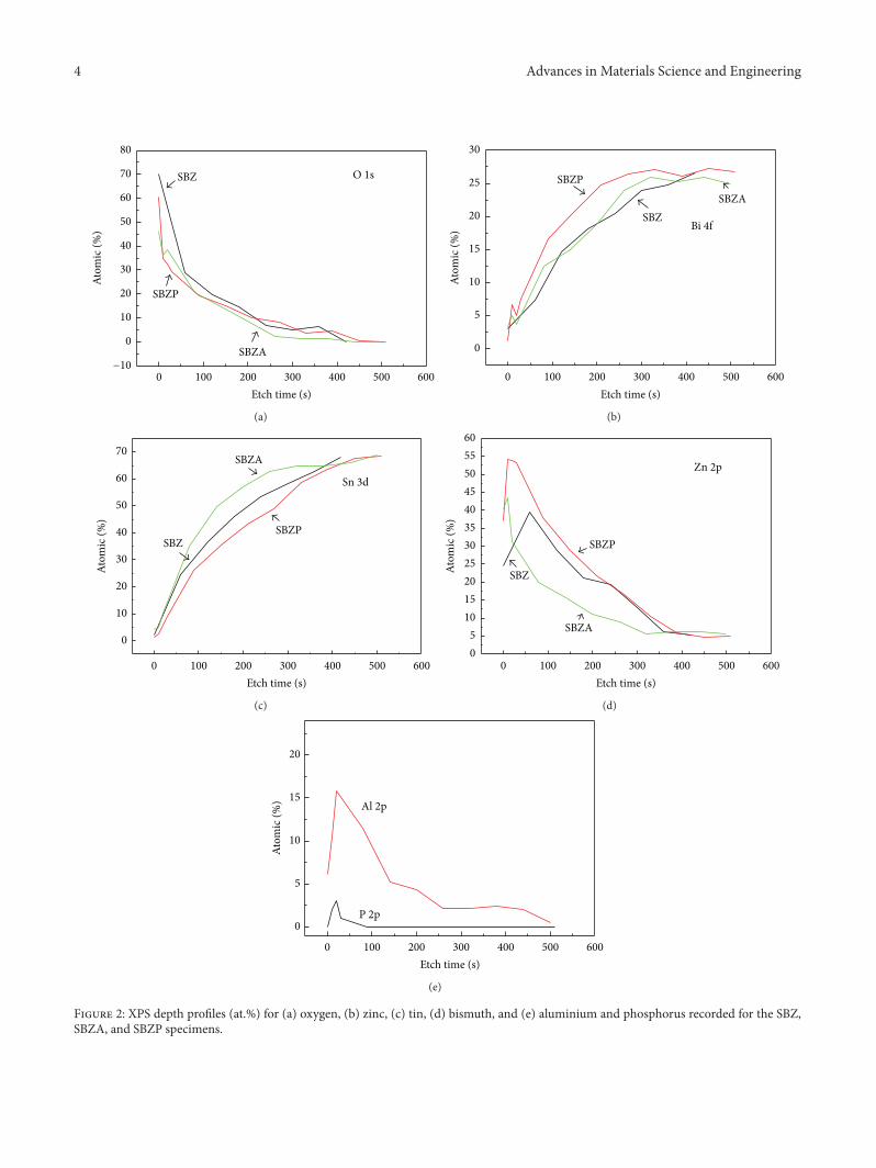
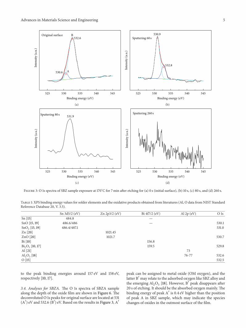
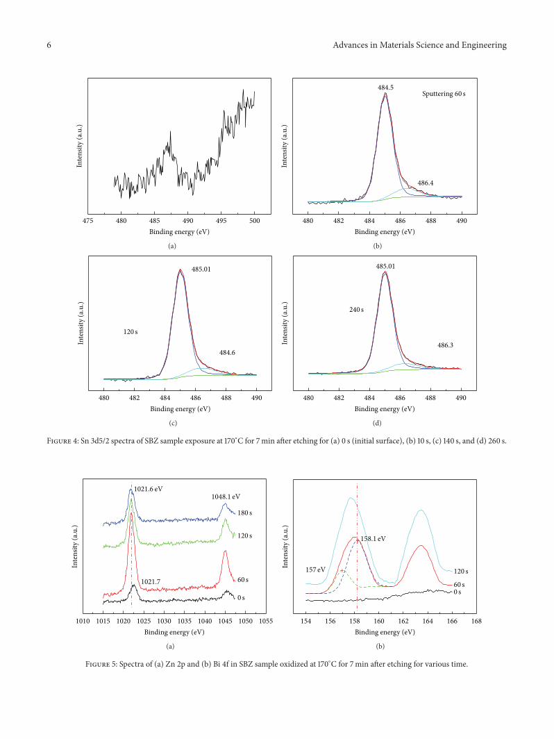
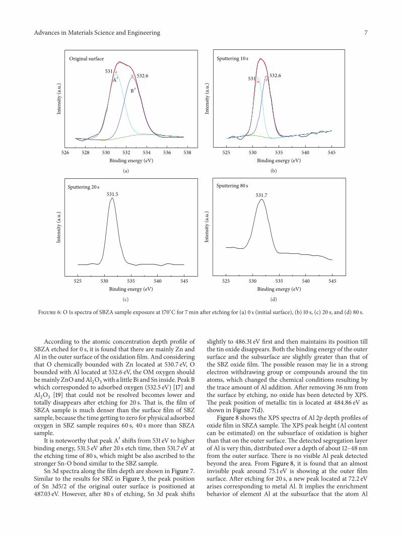
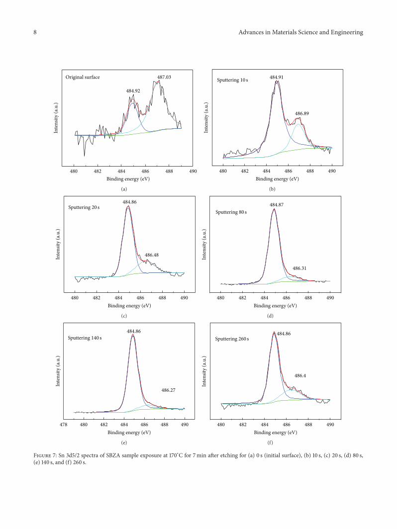
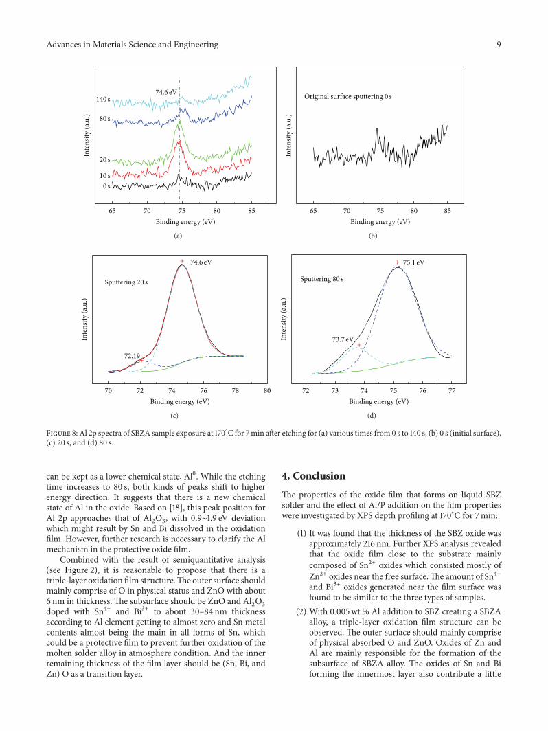