Embed Size (px)
Citation preview
Tel 248-295-0310 ■ Fax 248-624-9234 ■ [email protected] ■ www.acromag.com ■ 30765 Wixom Rd, Wixom, MI 48393 USA
XMC Modules
Bulletin #8400-819e
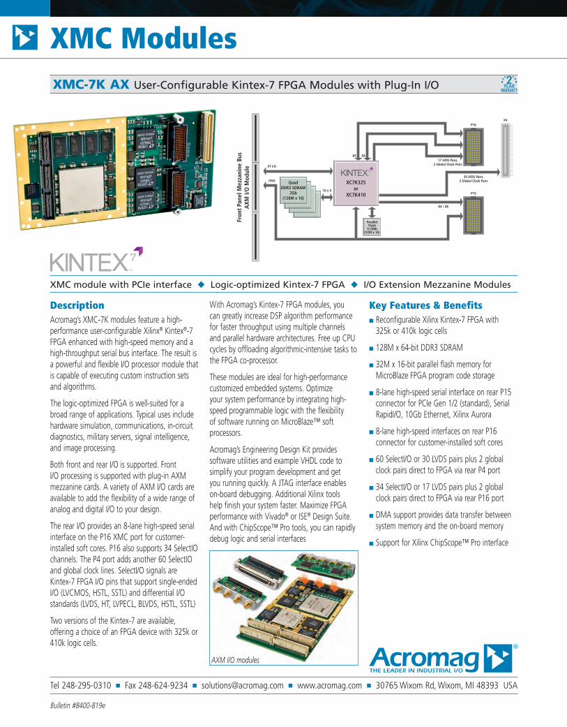
DescriptionAcromag’s XMC-7K modules feature a high-performance user-configurable Xilinx® Kintex®-7 FPGA enhanced with high-speed memory and a high-throughput serial bus interface. The result is a powerful and flexible I/O processor module that is capable of executing custom instruction sets and algorithms.
The logic-optimized FPGA is well-suited for a broad range of applications. Typical uses include hardware simulation, communications, in-circuit diagnostics, military servers, signal intelligence, and image processing.
Both front and rear I/O is supported. Front I/O processing is supported with plug-in AXM mezzanine cards. A variety of AXM I/O cards are available to add the flexibility of a wide range of analog and digital I/O to your design.
The rear I/O provides an 8-lane high-speed serial interface on the P16 XMC port for customer-installed soft cores. P16 also supports 34 SelectIO channels. The P4 port adds another 60 SelectIO and global clock lines. SelectI/O signals are Kintex-7 FPGA I/O pins that support single-ended I/O (LVCMOS, HSTL, SSTL) and differential I/O standards (LVDS, HT, LVPECL, BLVDS, HSTL, SSTL)
Two versions of the Kintex-7 are available, offering a choice of an FPGA device with 325k or 410k logic cells.
With Acromag’s Kintex-7 FPGA modules, you can greatly increase DSP algorithm performance for faster throughput using multiple channels and parallel hardware architectures. Free up CPU cycles by offloading algorithmic-intensive tasks to the FPGA co-processor.
These modules are ideal for high-performance customized embedded systems. Optimize your system performance by integrating high-speed programmable logic with the flexibility of software running on MicroBlaze™ soft processors.
Acromag’s Engineering Design Kit provides software utilities and example VHDL code to simplify your program development and get you running quickly. A JTAG interface enables on-board debugging. Additional Xilinx tools help finish your system faster. Maximize FPGA performance with Vivado® or ISE® Design Suite. And with ChipScope™ Pro tools, you can rapidly debug logic and serial interfaces
Key Features & Benefits■ Reconfigurable Xilinx Kintex-7 FPGA with
325k or 410k logic cells
■ 128M x 64-bit DDR3 SDRAM
■ 32M x 16-bit parallel flash memory for MicroBlaze FPGA program code storage
■ 8-lane high-speed serial interface on rear P15 connector for PCIe Gen 1/2 (standard), Serial RapidI/O, 10Gb Ethernet, Xilinx Aurora
■ 8-lane high-speed interfaces on rear P16 connector for customer-installed soft cores
■ 60 SelectI/O or 30 LVDS pairs plus 2 global clock pairs direct to FPGA via rear P4 port
■ 34 SelectI/O or 17 LVDS pairs plus 2 global clock pairs direct to FPGA via rear P16 port
■ DMA support provides data transfer between system memory and the on-board memory
■ Support for Xilinx ChipScope™ Pro interface
XMC module with PCIe interface ◆ Logic-optimized Kintex-7 FPGA ◆ I/O Extension Mezzanine Modules
XMC-7K AX User-Configurable Kintex-7 FPGA Modules with Plug-In I/O
AXM I/O modules
ParallelFlash
512Mb(32M x 16)
QuadDDR3 SDRAM
2Gb(128M x 16)
XC7K325or
XC7K410
97 I/O
JTAG
16 x 4
X4 X4
P15
P16P4
30 LVDS Pairs,2 Global Clock Pairs
17 LVDS Pairs,2 Global Clock Pairs
X4 / X8
Fron
t Pa
nel M
ezza
nine
Bus
AXM
I/O
Mod
ule
Tel 248-295-0310 ■ Fax 248-624-9234 ■ [email protected] ■ www.acromag.com ■ 30765 Wixom Rd, Wixom, MI 48393 USA
XMC Modules
All trademarks are property of their respective owners. Copyright © Acromag, Inc. 2015. Data subject to change without notice. Printed in USA 5/2015
XMC-7K AX User-Configurable Kintex-7 FPGA Modules w Plug-In I/O
Performance Specifications
■ FPGAFPGA deviceXilinx Kintex-7 FPGA.Model XC7K325T FPGA with 326,080 logic cells and 840 DSP48E1 slices or Model XC7K410T with 406,720 logic cells and 1540 DSP48E1 slices.FPGA configurationDownload via JTAG or flash memory.Example FPGA programIP integrator block diagram provided for bus interface, front & rear I/O control, and SDRAM memory interface controller. See EDK kit.
■ I/O ProcessingAcromag AXM I/O Modules:AXM modules plug into the XMC module’s front mezzanine for additional I/O lines. Analog and digital I/O AXM modules are sold separately.Rear high-speed I/O12 high-speed serial lanes. x8 lanes via P15 and x4 lanes via P16. Rear user I/OP16: 17 LVDS pairs (34 LVCMOS), 2 global clock pairs. P4: 30 LVDS pairs (60 LVCMOS), 2 global clock pairs.
■ Engineering Design KitProvides user with basic information required to develop a custom FPGA program. Kit must be ordered with the first purchase of a XMC-7K module (see www.acromag.com for more information).
■ XMC ComplianceComplies with ANSI/VITA 42.0 specification for XMC module mechanicals and connectors.Complies with ANSI/VITA 42.3 specification for XMC modules with PCI Express interface.Electrical/Mechanical Interface: Single-Width Module.
■ ElectricalXMC PCIe bus interface (P15 and P16)One 114-pin male connector (Samtec ASP-103614-05 or equivalent). P15 primary XMC connector8 differential pairs (PCIe standard, Serial RapidIO, 10-Gigabit Ethernet, or Xilinx Aurora). JTAG.System Management (XMC provides hardware definition information read by an external controller using IPMI commands and I2C serial bus transactions.)3.3V power: 4 pins at 1A/pin. 3.3V auxiliary power: 1 pin, powers volatile memory to store the bitstream encryption key. Variable power (5V or 12V): 8 pins at 1A per pin.P16 XMC connector4 differential pairs (PCIe, Serial RapidIO, or Xilinx Aurora).17 LVDS pairs or 34 SelectI/O signals (differential pairs grouped per VITA 46.0 X38s). 2 global clock pairs.Vcco pins are powered by 2.5V and support the 2.5V I/O standards.P4 PMC rear I/O connector64-pin female receptacle header (AMP 120527-1 or equivalent).64 I/O connections (30 LVDS pairs plus two global clocks). Vcco pins powered by 2.5V and support the 2.5V I/O standards.
■ EnvironmentalOperating temperatureXMC-7K325AX-LF: -40 to 50°C.XMC-7K410AX-LF: -40 to 40°CStorage temperature-55 to 125°C.Relative humidity5 to 95% non-condensing.Power3.3V (±5%): 7.8W typical. 12V (±5%): 2.7W typical3.3V AUX (±5%): 57µWMTBFContact the factory.
Ordering InformationNOTE: XMC-7K-EDK is required to configure FPGA.
■ XMC ModulesXMC-7K325AX-LFUser-configurable Kintex-7 FPGA, 325k logic cells with AXM supportXMC-7K410AX-LFUser-configurable Kintex-7 FPGA, 410k logic cells with AXM support
■ AccessoriesAXM-A7516 analog inputs, 8 analog outputs, and 16 digital I/OAXM-A302 analog input 100MHz 16-bit A/D channels.AXM-D0230 RS485 differential I/O channels.AXM-D0316 CMOS and 22 RS485 differential I/O channels. AXM-D0430 LVDS I/O channels. AXM-??Custom I/O configurations available, call factory.
■ SoftwareXMC-7KA-EDKEngineering Design Kit (one kit required)PMCSW-API-VXWVxWorks® 32-bit software support packagePCISW-API-WINWindows® DLL software support packagePCISW-LINUXLinux™ support (website download only)
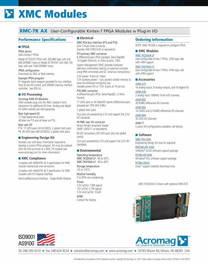
XMC-7K325AX-LF shown with optional AXM-A75
Tel 248-295-0310 ■ Fax 248-624-9234 ■ [email protected] ■ www.acromag.com ■ 30765 Wixom Rd, Wixom, MI 48393 USA
XMC Modules
Bulletin #8400-839c
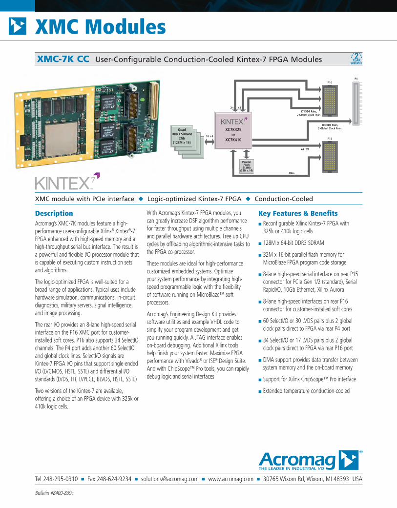
DescriptionAcromag’s XMC-7K modules feature a high-performance user-configurable Xilinx® Kintex®-7 FPGA enhanced with high-speed memory and a high-throughput serial bus interface. The result is a powerful and flexible I/O processor module that is capable of executing custom instruction sets and algorithms.
The logic-optimized FPGA is well-suited for a broad range of applications. Typical uses include hardware simulation, communications, in-circuit diagnostics, military servers, signal intelligence, and image processing.
The rear I/O provides an 8-lane high-speed serial interface on the P16 XMC port for customer-installed soft cores. P16 also supports 34 SelectIO channels. The P4 port adds another 60 SelectIO and global clock lines. SelectI/O signals are Kintex-7 FPGA I/O pins that support single-ended I/O (LVCMOS, HSTL, SSTL) and differential I/O standards (LVDS, HT, LVPECL, BLVDS, HSTL, SSTL)
Two versions of the Kintex-7 are available, offering a choice of an FPGA device with 325k or 410k logic cells.
With Acromag’s Kintex-7 FPGA modules, you can greatly increase DSP algorithm performance for faster throughput using multiple channels and parallel hardware architectures. Free up CPU cycles by offloading algorithmic-intensive tasks to the FPGA co-processor.
These modules are ideal for high-performance customized embedded systems. Optimize your system performance by integrating high-speed programmable logic with the flexibility of software running on MicroBlaze™ soft processors.
Acromag’s Engineering Design Kit provides software utilities and example VHDL code to simplify your program development and get you running quickly. A JTAG interface enables on-board debugging. Additional Xilinx tools help finish your system faster. Maximize FPGA performance with Vivado® or ISE® Design Suite. And with ChipScope™ Pro tools, you can rapidly debug logic and serial interfaces
Key Features & Benefits■ Reconfigurable Xilinx Kintex-7 FPGA with
325k or 410k logic cells
■ 128M x 64-bit DDR3 SDRAM
■ 32M x 16-bit parallel flash memory for MicroBlaze FPGA program code storage
■ 8-lane high-speed serial interface on rear P15 connector for PCIe Gen 1/2 (standard), Serial RapidI/O, 10Gb Ethernet, Xilinx Aurora
■ 8-lane high-speed interfaces on rear P16 connector for customer-installed soft cores
■ 60 SelectI/O or 30 LVDS pairs plus 2 global clock pairs direct to FPGA via rear P4 port
■ 34 SelectI/O or 17 LVDS pairs plus 2 global clock pairs direct to FPGA via rear P16 port
■ DMA support provides data transfer between system memory and the on-board memory
■ Support for Xilinx ChipScope™ Pro interface
■ Extended temperature conduction-cooled
XMC module with PCIe interface ◆ Logic-optimized Kintex-7 FPGA ◆ Conduction-Cooled
XMC-7K CC User-Configurable Conduction-Cooled Kintex-7 FPGA Modules
ParallelFlash
512Mb(32M x 16)
QuadDDR3 SDRAM
2Gb(128M x 16)
XC7K325or
XC7K410
JTAG
16 x 4
X4 X4
P15
P16P4
30 LVDS Pairs,2 Global Clock Pairs
17 LVDS Pairs,2 Global Clock Pairs
X4 / X8
Tel 248-295-0310 ■ Fax 248-624-9234 ■ [email protected] ■ www.acromag.com ■ 30765 Wixom Rd, Wixom, MI 48393 USA
XMC Modules
All trademarks are property of their respective owners. Copyright © Acromag, Inc. 2015. Data subject to change without notice. Printed in USA 5/2015
XMC-7K CC User-Configurable Conduction-Cooled Kintex-7 FPGA Modules
Performance Specifications
■ FPGAFPGA deviceXilinx Kintex-7 FPGA.Model XC7K325T FPGA with 326,080 logic cells and 840 DSP48E1 slices or Model XC7K410T with 406,720 logic cells and 1540 DSP48E1 slices.FPGA configurationDownload via JTAG or flash memory.Example FPGA programIP integrator block diagram provided for bus interface, front & rear I/O control, and SDRAM memory interface controller. See EDK kit.
■ I/O ProcessingRear high-speed I/O16 high-speed serial lanes. x8 lanes via P15 and x8 lanes via P16. Rear user I/OP16: 17 LVDS pairs (34 LVCMOS), 2 global clock pairs. P4: 30 LVDS pairs (60 LVCMOS), 2 global clock pairs.
■ Engineering Design KitProvides user with basic information required to develop a custom FPGA program. Kit must be ordered with the first purchase of a XMC-7K module (see www.acromag.com for more information).
■ XMC ComplianceComplies with ANSI/VITA 42.0 specification for XMC module mechanicals and connectors.Complies with ANSI/VITA 42.3 specification for XMC modules with PCI Express interface.Electrical/Mechanical Interface: Single-Width Module.
■ ElectricalXMC PCIe bus interface (P15 and P16)One 114-pin male connector (Samtec ASP-103614-05 or equivalent). P15 primary XMC connector8 differential pairs (PCIe standard, Serial RapidIO, 10-Gigabit Ethernet, or Xilinx Aurora). JTAG.System Management (XMC provides hardware definition information read by an external controller using IPMI commands and I2C serial bus transactions.)3.3V power: 4 pins at 1A/pin. 3.3V auxiliary power: 1 pin, powers volatile memory to store the bitstream encryption key. Variable power (5V or 12V): 8 pins at 1A per pin.P16 XMC connector4 differential pairs (PCIe, Serial RapidIO, or Xilinx Aurora).17 LVDS pairs or 34 SelectI/O signals (differential pairs grouped per VITA 46.0 X38s). 2 global clock pairs.Vcco pins are powered by 2.5V and support the 2.5V I/O standards.P4 PMC rear I/O connector64-pin female receptacle header (AMP 120527-1 or equivalent).64 I/O connections (30 LVDS pairs plus two global clocks). Vcco pins powered by 2.5V and support the 2.5V I/O standards.
■ EnvironmentalOperating temperatureXMC-7K325AX-LF: Conduction-cooled, -40 to 70°C.XMC-7K410AX-LF: Conduction-cooled, -40 to 70°CStorage temperature-55 to 125°C.Relative humidity5 to 95% non-condensing.Power3.3V (±5%): 7.8W typical. 12V (±5%): 2.7W typical.3.3V AUX (±5%): 57µWMTBFContact the factory.
Ordering InformationNOTE: XMC-7K-EDK is required to configure FPGA.
■ XMC ModulesXMC-7K325CC-LFUser-configurable Kintex-7 FPGA, 325k logic cells, conduction-cooledXMC-7K410CC-LFUser-configurable Kintex-7 FPGA, 410k logic cells, conduction-cooled
■ SoftwareXMC-7KA-EDKEngineering Design Kit (one kit required)PMCSW-API-VXWVxWorks® 32-bit software support packagePCISW-API-WINWindows® DLL software support packagePCISW-LINUXLinux™ support (website download only)
XMC-7K325CC-LF shown with heatsink
Tel 248-295-0310 ■ Fax 248-624-9234 ■ [email protected] ■ www.acromag.com ■ 30765 Wixom Rd, Wixom, MI 48393 USA
XMC Modules
Bulletin #8400-806d
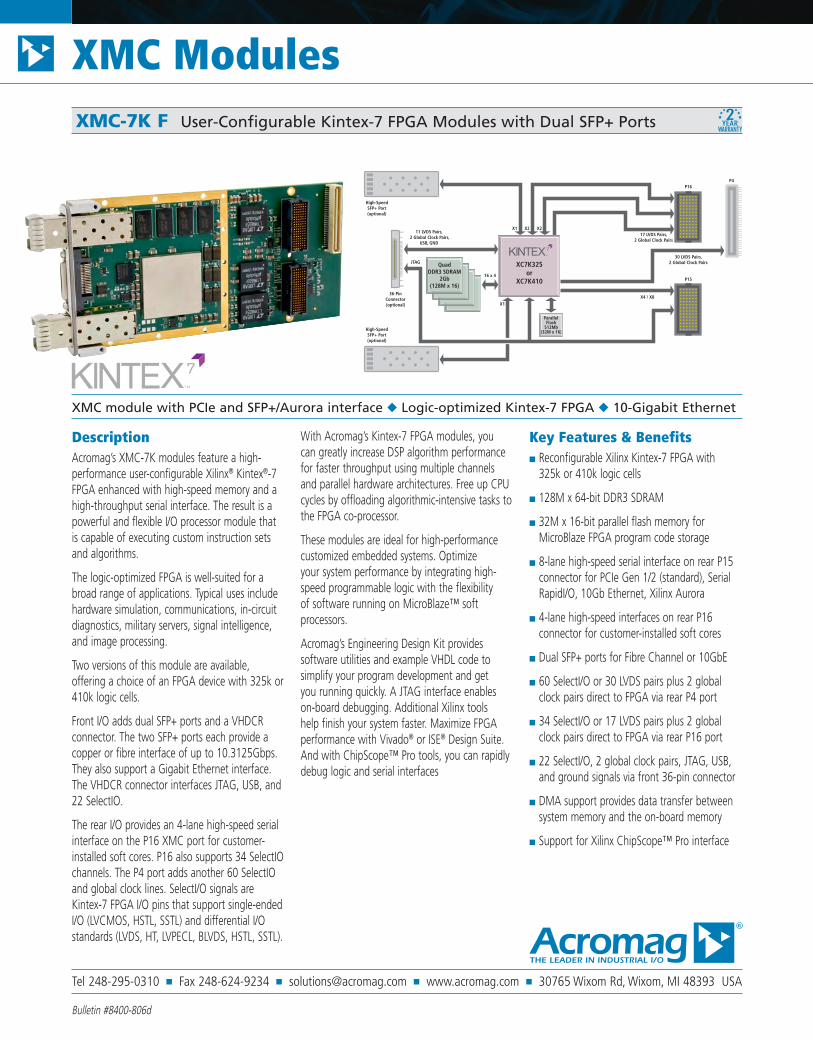
DescriptionAcromag’s XMC-7K modules feature a high-performance user-configurable Xilinx® Kintex®-7 FPGA enhanced with high-speed memory and a high-throughput serial interface. The result is a powerful and flexible I/O processor module that is capable of executing custom instruction sets and algorithms.
The logic-optimized FPGA is well-suited for a broad range of applications. Typical uses include hardware simulation, communications, in-circuit diagnostics, military servers, signal intelligence, and image processing.
Two versions of this module are available, offering a choice of an FPGA device with 325k or 410k logic cells.
Front I/O adds dual SFP+ ports and a VHDCR connector. The two SFP+ ports each provide a copper or fibre interface of up to 10.3125Gbps. They also support a Gigabit Ethernet interface. The VHDCR connector interfaces JTAG, USB, and 22 SelectIO.
The rear I/O provides an 4-lane high-speed serial interface on the P16 XMC port for customer-installed soft cores. P16 also supports 34 SelectIO channels. The P4 port adds another 60 SelectIO and global clock lines. SelectI/O signals are Kintex-7 FPGA I/O pins that support single-ended I/O (LVCMOS, HSTL, SSTL) and differential I/O standards (LVDS, HT, LVPECL, BLVDS, HSTL, SSTL).
With Acromag’s Kintex-7 FPGA modules, you can greatly increase DSP algorithm performance for faster throughput using multiple channels and parallel hardware architectures. Free up CPU cycles by offloading algorithmic-intensive tasks to the FPGA co-processor.
These modules are ideal for high-performance customized embedded systems. Optimize your system performance by integrating high-speed programmable logic with the flexibility of software running on MicroBlaze™ soft processors.
Acromag’s Engineering Design Kit provides software utilities and example VHDL code to simplify your program development and get you running quickly. A JTAG interface enables on-board debugging. Additional Xilinx tools help finish your system faster. Maximize FPGA performance with Vivado® or ISE® Design Suite. And with ChipScope™ Pro tools, you can rapidly debug logic and serial interfaces
Key Features & Benefits■ Reconfigurable Xilinx Kintex-7 FPGA with
325k or 410k logic cells
■ 128M x 64-bit DDR3 SDRAM
■ 32M x 16-bit parallel flash memory for MicroBlaze FPGA program code storage
■ 8-lane high-speed serial interface on rear P15 connector for PCIe Gen 1/2 (standard), Serial RapidI/O, 10Gb Ethernet, Xilinx Aurora
■ 4-lane high-speed interfaces on rear P16 connector for customer-installed soft cores
■ Dual SFP+ ports for Fibre Channel or 10GbE
■ 60 SelectI/O or 30 LVDS pairs plus 2 global clock pairs direct to FPGA via rear P4 port
■ 34 SelectI/O or 17 LVDS pairs plus 2 global clock pairs direct to FPGA via rear P16 port
■ 22 SelectI/O, 2 global clock pairs, JTAG, USB, and ground signals via front 36-pin connector
■ DMA support provides data transfer between system memory and the on-board memory
■ Support for Xilinx ChipScope™ Pro interface
XMC module with PCIe and SFP+/Aurora interface ◆ Logic-optimized Kintex-7 FPGA ◆ 10-Gigabit Ethernet
XMC-7K F User-Configurable Kintex-7 FPGA Modules with Dual SFP+ Ports
ParallelFlash
512Mb(32M x 16)
QuadDDR3 SDRAM
2Gb(128M x 16)
XC7K325or
XC7K410
High-SpeedSFP+ Port(optional)
High-SpeedSFP+ Port(optional)
11 LVDS Pairs, 2 Global Clock Pairs,
USB, GND
36-PinConnector(optional)
JTAG
16 x 4
X1
X1 X2 X2
P15
P16P4
30 LVDS Pairs,2 Global Clock Pairs
17 LVDS Pairs,2 Global Clock Pairs
X4 / X8
Tel 248-295-0310 ■ Fax 248-624-9234 ■ [email protected] ■ www.acromag.com ■ 30765 Wixom Rd, Wixom, MI 48393 USA
XMC Modules
All trademarks are property of their respective owners. Copyright © Acromag, Inc. 2015. Data subject to change without notice. Printed in USA 5/2015
XMC-7K F User-Configurable Kintex-7 FPGA Modules w Dual SFP+ Ports
Performance Specifications
■ FPGAFPGA deviceXilinx Kintex-7 FPGA.Model XC7K325T FPGA with 326,080 logic cells and 840 DSP48E1 slices or Model XC7K410T with 406,720 logic cells and 1540 DSP48E1 slices.FPGA configurationDownload via JTAG or flash memory.Example FPGA programIP integrator block diagram provided for bus interface, front & rear I/O control, and SDRAM memory interface controller. See EDK kit.
■ I/O ProcessingFront high-speed I/OTwo x1 lanes via SFP+ connectors for Gigabit Ethernet and Fibre Channel interfaceFront user I/O36-pin connector provides JTAG connection, USB signals, 2 global differential clock pairs, 11 LVDS signal pairs, and 2 ground signals.Rear high-speed I/O12 high-speed serial lanes. x8 lanes via P15 and x4 lanes via P16. Rear user I/OP16: 17 LVDS pairs (34 LVCMOS), 2 global clock pairs. P4: 30 LVDS pairs (60 LVCMOS), 2 global clock pairs.
■ Engineering Design KitProvides user with basic information required to develop a custom FPGA program. Kit must be ordered with the first purchase of a XMC-7K module (see www.acromag.com for more information).
■ XMC ComplianceComplies with ANSI/VITA 42.0 specification for XMC module mechanicals and connectors.Complies with ANSI/VITA 42.3 specification for XMC modules with PCI Express interface.Electrical/Mechanical Interface: Single-Width Module.
■ ElectricalXMC PCIe bus interface (P15 and P16)One 114-pin male connector (Samtec ASP-103614-05 or equivalent). P15 primary XMC connector8 differential pairs (PCIe standard, Serial RapidIO, 10-Gigabit Ethernet, or Xilinx Aurora). JTAG.System Management (XMC provides hardware definition information read by an external controller using IPMI commands and I2C serial bus transactions.)3.3V power: 4 pins at 1A/pin. 3.3V auxiliary power: 1 pin for system management. Variable power (5V or 12V): 8 pins at 1A per pin.P16 XMC connector4 differential pairs (PCIe, Serial RapidIO, or Xilinx Aurora).17 LVDS pairs or 34 SelectI/O signals (differential pairs grouped per VITA 46.0 X38s). 2 global clock pairs.Vcco pins are powered by 2.5V and support the 2.5V I/O standards.P4 PMC rear I/O connector64-pin female receptacle header (AMP 120527-1 or equivalent).64 I/O connections (30 LVDS pairs plus two global clocks). Vcco pins powered by 2.5V and support the 2.5V I/O standards.VHDCR connector36-position connector (Samtec VHDCR-36-01-M-RA) mates with industry-standard VHDCI cable assemblies.SFP+ host connectorSFP transceiver signals route directly to Kintex-7 FPGA. 10.3125Gb/S maximum data rate.SFP+ copper (Gigabit Ethernet) or fibre optic modules available from Acromag.
■ EnvironmentalOperating temperatureXMC-7K325F-LF: -40 to 50°C.XMC-7K410F-LF: -40 to 40°C.
Storage temperature-55 to 125°C.Relative humidity5 to 95% non-condensing.Power3.3V (±5%): 7.8W typical. 12V (±5%): 2.7W typical.3.3V AUX (±5%): 57µW typical.MTBFContact the factory.
Ordering InformationNOTE: XMC-7K-EDK is required to configure FPGA.
■ XMC ModulesXMC-7K325F-LFUser-configurable Kintex-7 FPGA, 325k logic cells plus SFP front I/OXMC-7K410F-LFUser-configurable Kintex-7 FPGA, 410k logic cells plus SFP front I/O
■ Accessories5025-921Cable, VHDCI 36-pin to SCSI-2, 6 feet long.5028-449Cable, copper twin-ax, SFP to SFP, 1 meter long.5028-455Transceiver, 10/100/1000BASE-T copper SFP, up to 1.25Gb/s bi-directional data links. 5028-452Transceiver, short-wavelength SFP, up to 2.125Gb/s bi-directional data links.
■ SoftwareXMC-7KA-EDKEngineering Design Kit (one kit required)PMCSW-API-VXWVxWorks® 32-bit software support packagePCISW-API-WINWindows® DLL software support packagePCISW-LINUXLinux™ support (website download only)
XMC-7K325F-LF shown with heatsink