Embed Size (px)
Citation preview

TIDUA66 – June 2015 1 Xilinx® Zynq®7000 series 5W Small, Efficient, Low-Noise Power Solution Copyright © 2015, Texas Instruments Incorporated
TI Designs
Xilinx® Zynq®7000 series 5W Small, Efficient, Low-Noise Power Solution
TI Designs
TI Designs provide the foundation that you need including methodology, testing and design files to quickly evaluate and customize the system. TI Designs help you accelerate your time to market.
Design Resources
TIDA-00574 Design Folder LP8758 Product Folder LP5907 Product Folder LP3990 Product Folder LMZ31503 Product Folder
High level Block Diagram
Design Features
Output voltage ranges from 0.6V to 3.36V
Output voltage adjustable via I2C interface
Startup & Shutdown Programmable delays for sequencing capability
Maximum output current 4A per phase
Output voltage Enable/Disable control
Ultra Low Noise, Low Iq LDO
Featured Applications
FPGA Power o For Zynq Z-7010,Z-7015,Z-7020
ASIC/SoC Power Management
Board Image
Ask The Analog Experts
Linear Regulators - Forum
WEBENCH® Design Center
Lit Number: TIDUA66 Date: June 2015

www.ti.com
TIDUA66 - June 2015 2 Xilinx® Zynq®7000 series 5W Small, Efficient, Low-Noise Power Solution Copyright © 2015, Texas Instruments Incorporated
Table of contents Table of contents __________________________________________________________________ 2
1 System Description _____________________________________________________________ 3
1.1 TI Design Overview _________________________________________________________ 3
2 Block Diagram _________________________________________________________________ 4
3 Component Selection ___________________________________________________________ 4
3.1 LP8758 __________________________________________________________________ 5
3.2 LP5907 __________________________________________________________________ 6
3.3 LP3990 __________________________________________________________________ 6
3.4 LMZ31503 ________________________________________________________________ 7
4 System design and component selection ____________________________________________ 8
4.1 Input voltage consideration __________________________________________________ 8
4.2 Inductor & Input/output Capacitor selection consideration for Buck regulator __________ 8
4.2.1 LP8758 Inductor Selection _______________________________________________ 8
4.2.2 LP8758 Input Capacitor Selection __________________________________________ 9
4.2.3 LP8758 Output capacitors ______________________________________________ 10
4.3 Low-Noise Linear Regulator Components Selection ______________________________ 10
4.3.1 LP5907 & LP3990 Input capacitor_________________________________________ 10
4.3.1 LP5907 & LP3990 Output capacitor _______________________________________ 10
4.4 System Output voltage configuration _________________________________________ 11
5 Power up Sequence ___________________________________________________________ 11
6 Layout guidelines _____________________________________________________________ 11
6.1 LP8758 Layout Example ____________________________________________________ 11
6.2 LP5907 & LP3990 Layout Example ____________________________________________ 13
7 Test Results __________________________________________________________________ 14
7.1 Equipment used __________________________________________________________ 14
7.2 Power up and Shutdown Sequence ___________________________________________ 14
7.3 Efficiency ________________________________________________________________ 18
7.4 Ripple Voltage ____________________________________________________________ 19
7.5 Voltage Output accuracy ___________________________________________________ 20
7.6 Load Transients ___________________________________________________________ 21
7.7 Thermal Image ___________________________________________________________ 22
8 Design Files __________________________________________________________________ 24
8.1 Schematics ______________________________________________________________ 24
8.2 Bill of Materials ___________________________________________________________ 25
9 Gerber Files __________________________________________________________________ 25
9.1 Layout Prints _____________________________________________________________ 25
10 Terminology _______________________________________________________________ 25
11 About the Author ___________________________________________________________ 25
www.ti.com
TIDUA66 - June 2015 3 Xilinx® Zynq®7000 series 5W Small, Efficient, Low-Noise Power Solution Copyright © 2015, Texas Instruments Incorporated
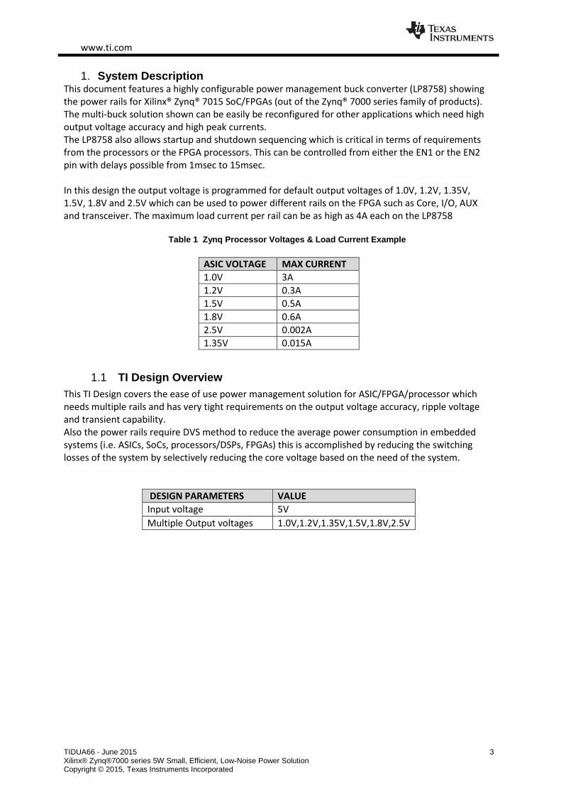
1. System Description This document features a highly configurable power management buck converter (LP8758) showing the power rails for Xilinx® Zynq® 7015 SoC/FPGAs (out of the Zynq® 7000 series family of products). The multi-buck solution shown can be easily be reconfigured for other applications which need high output voltage accuracy and high peak currents. The LP8758 also allows startup and shutdown sequencing which is critical in terms of requirements from the processors or the FPGA processors. This can be controlled from either the EN1 or the EN2 pin with delays possible from 1msec to 15msec. In this design the output voltage is programmed for default output voltages of 1.0V, 1.2V, 1.35V, 1.5V, 1.8V and 2.5V which can be used to power different rails on the FPGA such as Core, I/O, AUX and transceiver. The maximum load current per rail can be as high as 4A each on the LP8758
Table 1 Zynq Processor Voltages & Load Current Example
ASIC VOLTAGE MAX CURRENT
1.0V 3A
1.2V 0.3A
1.5V 0.5A
1.8V 0.6A
2.5V 0.002A
1.35V 0.015A
1.1 TI Design Overview
This TI Design covers the ease of use power management solution for ASIC/FPGA/processor which needs multiple rails and has very tight requirements on the output voltage accuracy, ripple voltage and transient capability. Also the power rails require DVS method to reduce the average power consumption in embedded systems (i.e. ASICs, SoCs, processors/DSPs, FPGAs) this is accomplished by reducing the switching losses of the system by selectively reducing the core voltage based on the need of the system.
DESIGN PARAMETERS VALUE
Input voltage 5V
Multiple Output voltages 1.0V,1.2V,1.35V,1.5V,1.8V,2.5V

www.ti.com
TIDUA66 - June 2015 4 Xilinx® Zynq®7000 series 5W Small, Efficient, Low-Noise Power Solution Copyright © 2015, Texas Instruments Incorporated
2 Block Diagram
Figure 1 Comprehensive block diagram
3 Component Selection This TI design has the following components Multi-Rail Power Management Buck Converter: LP8758 Four Output Step down DC-DC Regulator
Parameters taken into account when selecting the buck regulator:
Low Iq in Shutdown mode
High accuracy in steady state
Startup & Shutdown sequencing capability.
Vout Range with DVS Control
Small Solution Size
Alternative parts with similar functionality
LP8754 similar functionality with additional phases Low Noise Linear Regulator for low power current rails : The LP5907 Ultra Low-Noise, 250-mA Linear Regulator for RF and Analog Circuits
Parameters taken into account when selecting the LDO
Low Output Voltage Noise
High PSRR
Output Voltage Tolerance
Virtually Zero IQ (Disabled): < 1 µA

www.ti.com
TIDUA66 - June 2015 5 Xilinx® Zynq®7000 series 5W Small, Efficient, Low-Noise Power Solution Copyright © 2015, Texas Instruments Incorporated
The LP3990 is 150 mA Linear Voltage Regulator for Digital Applications Parameters taken into account when selecting the LDO
High PSRR
Output Voltage Tolerance
Output Voltage from 0.8V to 3.3V
Virtually Zero IQ (Disabled), < 10 nA The alternative parts must have an adjustable pin:
LP5900 has similar functionality at lower load currents (150mA)
Step Down Voltage Power Module: LMZ31503 Power Module with 4.5V-14.5V Input in small package
Parameters taken into account when selecting the buck regulator:
High Efficiency
High accuracy in steady state
Small Solution Size
3.1 LP8758
The LP8758 is a high-efficiency, high-performance power supply device with four step-down DC-DC converter cores. The cores are configured for a four single-phase configuration. The device delivers 0.5-V to 3.36-V regulated voltage rails from 2.5-V to 5.5-V battery. There are two modes of operation for the converter, depending on the output current required: Pulse-Width Modulation (PWM) and Pulse-Frequency Modulation (PFM). The converter operates in PWM mode at high load currents of approximately 400 mA or higher. Lighter output current loads will cause the converter to automatically switch into PFM mode for reduced current consumption and a longer battery life when Forced PWM mode is disabled. Additional features include soft-start, under voltage lockout, overload protection, thermal warning, and thermal shutdown.
Figure 2 : LP8758 Functional Block Diagram

www.ti.com
TIDUA66 - June 2015 6 Xilinx® Zynq®7000 series 5W Small, Efficient, Low-Noise Power Solution Copyright © 2015, Texas Instruments Incorporated
3.2 LP5907
The LP5907 is a linear regulator capable of supplying 250-mA output current. Designed to meet the requirements of RF and analog circuits, the LP5907 device provides low noise, high PSRR, low quiescent current and low line or load transient response figures. Using new innovative design techniques, the LP5907 offers class-leading noise performance without a noise bypass capacitor and the ability for remote output capacitor placement.
Figure 3: LP5907 Functional block diagram
3.3 LP3990
The LP3990 regulator is designed to meet the 1% Voltage Accuracy at Room Temperature requirements of portable, battery-powered systems providing an accurate output voltage, low-noise, and low-quiescent current. The LP3990 will provide a 0.8 V output from the low input voltage of 2 V at up to a 150-mA load current. When switched into shutdown mode via a logic signal at the enable pin (EN), the power consumption is reduced to virtually zero. The LP3990 is designed to be stable with space-saving ceramic capacitors with values as low as 1 µF.
Figure 4: LP3990 Functional Block Diagram

www.ti.com
TIDUA66 - June 2015 7 Xilinx® Zynq®7000 series 5W Small, Efficient, Low-Noise Power Solution Copyright © 2015, Texas Instruments Incorporated
3.4 LMZ31503
The LMZ31503 SIMPLE SWITCHER® power module is an easy-to-use integrated power solution that combines a 3-A DC/DC converter with power MOSFETs, a shielded inductor, and passives into a low profile, QFN package. This total power solution allows as few as 3 external components and eliminates the loop compensation and magnetics design process. The LMZ31503 has a wide output voltage adjustable options from 0.8 V to 5.5 V, in this design it is set to regulate an input voltage of 12V to 5V at up to a 3 A load current.
Figure 5: LMZ31503 Functional Block Diagram

www.ti.com
TIDUA66 - June 2015 8 Xilinx® Zynq®7000 series 5W Small, Efficient, Low-Noise Power Solution Copyright © 2015, Texas Instruments Incorporated
4 System design and component selection The following system considerations apply only for the conditions of this design. For different conditions it is essential to verify the ratings and operating conditions on the datasheets of the parts mentioned in this design. If the parameters does not fit the application consider one of the alternative parts on section 3 or perform and easy parametric search at http://www.ti.com
4.1 Input voltage consideration
The LP8758 device is designed to operate from an input voltage supply range between 2.5 V and 5.5 V. This input supply should be well-regulated and able to withstand maximum input current and maintain stable voltage without voltage drop even at load transition condition. The resistance of the input supply rail should be low enough that the input current transient does not cause too high drop in the LP8758, LP5907 or LP3990 supply voltage that can cause false UVLO fault triggering. If the input supply is located more than a few inches from the LP8758, LP5907 or LP3990 additional bulk capacitance may be required in addition to the ceramic bypass capacitors.
4.2 Inductor & Input/output Capacitor selection consideration for Buck regulator
4.2.1 LP8758 Inductor Selection
DC bias current characteristics of inductors must be considered. Different manufacturers follow different saturation current rating specifications, so attention must be given to details. DC bias curves should be requested from them as part of the inductor selection process. Minimum effective value of inductance to ensure good performance is 0.22 μH at 4 A bias current over the inductor's operating temperature range. The inductor’s DC resistance should be less than 0.05 Ω for good efficiency at high current condition. The inductor AC loss (resistance) also affects conversion efficiency. Higher Q factor at switching frequency usually gives better efficiency at light load to middle loads
Table 2: Recommended Inductors

www.ti.com
TIDUA66 - June 2015 9 Xilinx® Zynq®7000 series 5W Small, Efficient, Low-Noise Power Solution Copyright © 2015, Texas Instruments Incorporated
4.2.2 LP8758 Input Capacitor Selection
A ceramic input capacitor of 10 μF, 6.3 V is sufficient for most applications. Place the power input capacitor as close as possible to the VIN_Bx pin and PGND_Bx pin of the device. A larger value or higher voltage rating may be used to improve input voltage filtering. Use X7R or X5R types, do not use Y5V or F. DC bias characteristics of ceramic capacitors must be considered when selecting case sizes
like 0402. Minimum effective input capacitance to ensure good performance is 1.9 μF per buck input at maximum input voltage DC bias including tolerances and over ambient temp range, assuming that
there are at least 22 μF of additional capacitance common for all the power input pins on the system power rail.
Table 3: Recommended Power Input Capacitors (X5R Dielectric)
The input filter capacitor supplies current to the high-side FET switch in the first half of each cycle and reduces voltage ripple imposed on the input power source. A ceramic capacitor's low equivalent series resistance (ESR) provides the best noise filtering of the input voltage spikes due to this rapidly changing current. Select an input filter capacitor with sufficient ripple current rating. The VANA input is used to supply analog and digital circuits in the device. See recommended components from table below for VANA input supply filtering
Table 4: Recommended VANA Supply Filtering Components

www.ti.com
TIDUA66 - June 2015 10 Xilinx® Zynq®7000 series 5W Small, Efficient, Low-Noise Power Solution Copyright © 2015, Texas Instruments Incorporated
4.2.3 LP8758 Output capacitors
Use ceramic capacitors, X7R or X5R types; do not use Y5V or F. DC bias voltage characteristics of ceramic capacitors must be considered. DC bias characteristics vary from manufacturer to manufacturer, and DC bias curves should be requested from them as part of the capacitor selection process. The output filter capacitor smooth’s out current flow from the inductor to the load, helps maintain a steady output voltage during transient load changes and reduces output voltage ripple. These capacitors must be selected with sufficient capacitance and sufficiently low ESR and ESL to
perform these functions. Minimum effective output capacitance to ensure good performance is 10 μF
per phase at the output voltage DC bias including tolerances and over ambient temp range. The output voltage ripple is caused by the charging and discharging of the output capacitor and also due to its RESR. The RESR is frequency dependent (as well as temperature dependent); make sure the value used for selection process is at the switching frequency of the part. A higher output capacitance improves the load step behavior and reduces the output voltage ripple as
well as decreases the PFM switching frequency. For most 4-phase applications 4 x 22 μF 0603
capacitors for COUT are suitable. Although a converter's loop compensation can be programmed to adapt to virtually several hundreds of microfarads COUT, it is preferable for COUT to be < 200 μF (4-phase configuration). Choosing higher than that is not necessarily of any benefit. Note that the output capacitor may be the limiting factor in the output voltage ramp, especially for very large (> 100 μF) output capacitors. For large output capacitors, the output voltage might be slower than the programmed ramp rate at voltage transitions, because of the higher energy stored on the output capacitance. Also at start-up, the time required to charge the output capacitor to target value might be longer. At shutdown, if the output capacitor is discharged by the internal discharge resistor, more time is required to settle VOUT down as a consequence of the increased time constant.
Table 5: Recommended Output Capacitors (X5R Dielectric)
4.3 Low-Noise Linear Regulator Components Selection
4.3.1 LP5907 & LP3990 Input capacitor
An input capacitor is required for stability. The input capacitor should be at least equal to, or greater than, the output capacitor for good load transient performance. At least a 1 µF capacitor has to be connected between the LDO input pin and ground for stable operation over full load current range. Basically, it is ok to have more output capacitance than input, as long as the input is at least 1 µF. The input capacitor must be located a distance of not more than 1 cm from the input pin and returned to a clean analog ground. Any good quality ceramic, tantalum, or film capacitor may be used at the input
4.3.1 LP5907 & LP3990 Output capacitor
The LP5907, LP3990 is designed specifically to work with a very small ceramic output capacitor, typically 1 µF. A ceramic capacitor (dielectric types X5R or X7R) in the 1 µF to 10 µF range, and with ESR between 5 mΩ to 500 mΩ, is suitable in the application circuit. For this device the output capacitor should be connected between the OUT pin and a good connection back to the GND pin. It may also be possible to use tantalum or film capacitors at the device output, VOUT, but these are not as attractive for reasons of size and cost

www.ti.com
TIDUA66 - June 2015 11 Xilinx® Zynq®7000 series 5W Small, Efficient, Low-Noise Power Solution Copyright © 2015, Texas Instruments Incorporated
4.4 System Output voltage configuration
The LP8758 is configured as 4 single phase buck regulator and the default output voltages are 1.0V, 1.2V, 1.5V and 1.8V. The startup slew rate for the output voltage is set as 10mV/µsec and the current limits can be set from 1.5A to 5.0A according to the requirements from the SoC/Processor. The buck regulators can be enabled via I2C and/or EN1/2 pins and this can be set as default in the device. In addition the low current rails of 1.35V and 2.5V are powered off the linear regulator to have a small solution size and keep the BOM cost low. Additional voltage options are available on the LP5907 or LP3990 if any other voltage is needed for additional design. LP5907 device is available with fixed output voltages from 1.20 V to 4.50 V in 25-mV steps. Contact Texas Instruments Sales for specific voltage option needs. LP3990 is available in output voltages 0.8 V, 1.2 V, 1.35 V, 1.5 V, 1.8 V, 2.5 V, 2.8 V, or 3.3 V, and for other voltage options please contact the Texas Instruments sales office
5 Power up Sequence The power-up sequence for the LP8758 is as follows:
VANA (and VIN_Bx) reach min recommended levels (V(VANA) > VANAUVLO). NRST is set to high level. This initiates Power-On-Reset (POR), OTP reading and enables the
system I/O interface. The I2C host should allow at least 700 μs before writing or reading data to the LP8758.
Device enters STANDBY-mode. The host can change the default register setting by I2C if needed. The regulator can be enabled/disabled by ENx pin(s) and by I2C interface
For the LP5907 and the LP3990 the VIN pin should be connected to voltage > 2.2V and the EN pin needs to connected high > 1.2V to turn on the linear regulators
6 Layout guidelines
6.1 LP8758 Layout Example
The high frequency and large switching currents of the LP8758 make the choice of layout important. Good power supply results will only occur when care is given to proper design and layout. Layout will affect noise pickup and generation and can cause a good design to perform with less-than-expected results. With a range of output currents from milliamps to 10A and over, good power supply layout is much more difficult than most general PCB design. The following steps should be used as a reference to ensure the device is stable and maintains proper voltage and current regulation across its intended operating voltage and current range.
Place CIN as close as possible to the VIN_Bx pin and the PGND_Bxx pin. Route the VIN trace wide and thick to avoid IR drops. The trace between the input capacitor's positive node and LP8758’s VIN_Bx pin(s) as well as the trace between the input capacitor's negative node and power PGND_Bxx pin(s) must be kept as short as possible. The input capacitance provides a low-impedance voltage source for the switching converter. The inductance of the connection is the most important parameter of a local decoupling capacitor – parasitic inductance on these traces must be kept as tiny as possible for proper device operation.
The output filter, consisting of Lx and COUTx, converts the switching signal at SW_Bx to the noiseless output voltage. It should be placed as close as possible to the device keeping the switch node small, for best EMI behavior. Route the traces between the LP8758's output capacitors and the load's input capacitors direct and wide to avoid losses due to the IR drop.
Input for analog blocks (VANA and AGND) should be isolated from noisy signals. Connect VANA directly to a quiet system voltage node and AGND to a quiet ground point where no IR drop occurs. Place the decoupling capacitor as close to the VANA pin as possible. VANA must be connected to the same power node as VIN_Bx pins.

www.ti.com
TIDUA66 - June 2015 12 Xilinx® Zynq®7000 series 5W Small, Efficient, Low-Noise Power Solution Copyright © 2015, Texas Instruments Incorporated
If the processor load supports remote voltage sensing, connect the LP8758’s feedback pins FB_Bx to the respective sense pins on the processor. The sense lines are susceptible to noise. They must be kept away from noisy signals such as PGND_Bxx, VIN_Bx, and SW_Bx, as well as high bandwidth signals such as the I2C. Avoid both capacitive as well as inductive coupling by keeping the sense lines short, direct and close to each other. Run the lines in a quiet layer. Isolate them from noisy signals by a voltage or ground plane if possible. Running the signal as a differential pair is recommended.
PGND_Bxx, VIN_Bx and SW_Bx should be routed on thick layers. They must not surround inner signal layers which are not able to withstand interference from noisy PGND_Bxx, VIN_Bx and SW_Bx.
Due to the small package of this converter and the overall small solution size, the thermal performance of the PCB layout is important. Many system-dependent issues such as thermal coupling, airflow, added heat sinks and convection surfaces, and the presence of other heat-generating components affect the power dissipation limits of a given component. Proper PCB layout, focusing on thermal performance, results in lower die temperatures. Wide power traces come with the ability to sink dissipated heat. This can be improved further on multi-layer PCB designs with vias to different planes. This results in reduced junction-to-ambient (RθJA) and junction-to-board (RθJB) thermal resistances and thereby reduces the device junction temperature, TJ. Performing a careful systemlevel 2D or full 3D dynamic thermal analysis at the beginning product design process is strongly recommended, using a thermal modeling analysis software
Via to GND plane
Via to VIN plane
CIN0
COUT3 COUT2
COUT1 COUT0
L2L3
L1 L0
VOUT0
VIN VIN
VINVIN
GND
CIN4
Pin A1
VIN
_B0
EN1
EN2
VIN
_B2
SW
_B0
SW
_B0
FB
_B0
FB
_B2
SW
_B2
FB
_B1
FB
_B3
PGND
_B01
PGND
_B01
SDA
SCL
PGND
_B23
SW
_B1
SW
_B1
nINTAGND
SW
_B3
VIN
_B1
VANA
NRST
VIN
_B3
VIN
_B0
VIN
_B2
SW
_B2
PGND
_B23
SW
_B3
VIN
_B3
PGND
_B23
PGND
_B01SGND
VIN
_B1
CIN2CIN3
CIN1
VOUT1
VOUT2VOUT3
GND
CVANA
CIN5
GND
VIN
VIN
VIN
GND
Figure 6: PCB layout example for LP8758

www.ti.com
TIDUA66 - June 2015 13 Xilinx® Zynq®7000 series 5W Small, Efficient, Low-Noise Power Solution Copyright © 2015, Texas Instruments Incorporated
6.2 LP5907 & LP3990 Layout Example
Figure 7: PCB Layout Example for LP5907
Figure 8 : PCB Layout Example for LP3990

www.ti.com
TIDUA66 - June 2015 14 Xilinx® Zynq®7000 series 5W Small, Efficient, Low-Noise Power Solution Copyright © 2015, Texas Instruments Incorporated
7 Test Results
7.1 Equipment used
Table 5 is a list of the test equipment used in the preceding sections.
Table 5 Test equipment
TEST EQUIPMENT PART NUMBER
Oscilloscope Agilent DPO4014B
Voltage supply Agilent E3631A
Multimeters Agilent E34401A
7.2 Power up and Shutdown Sequence
Table 6 shows the power up default settings of the system.
Table 6 Default output voltage settings
VOUT EN PIN SELECT STARTUP DELAY SHUTDOWN DELAY
1.0V EN1 0 msec 5 msec
1.8V EN1 5 msec 0 msec
1.2V EN2 0 msec 0 msec
1.5V EN2 0 msec 0 msec
2.5V EN2 0 msec 0 msec
1.35V EN2 0 msec 0 msec
The table shows the default power up voltages for the LP8758 and the two LDO’s: LP5907 & LP3990.The delays are set from the ENx pin and these can be set using different register settings which allows programmability from 1msec to 15msec for startup & shutdown sequence. Also the LP5907 & LP3990 EN pins are connected to LP8758 EN2 pin to control the 2.5V and 1.35V rails power up sequence. With the following design no external sequencer is needed and it reduces the overall BOM cost for the design.

www.ti.com
TIDUA66 - June 2015 15 Xilinx® Zynq®7000 series 5W Small, Efficient, Low-Noise Power Solution Copyright © 2015, Texas Instruments Incorporated
Figure 9 : Example Startup Sequence
Figure 10: Example Shutdown Sequence

www.ti.com
TIDUA66 - June 2015 16 Xilinx® Zynq®7000 series 5W Small, Efficient, Low-Noise Power Solution Copyright © 2015, Texas Instruments Incorporated
Figure 11: Measured Startup Sequence
Figure 12: Measured Startup Sequence (Continue)
EN1
Vout =1.0V
Vout =1.8V
EN2
Vout =1.2V
Vout =1.5V
Vout =2.5V

www.ti.com
TIDUA66 - June 2015 17 Xilinx® Zynq®7000 series 5W Small, Efficient, Low-Noise Power Solution Copyright © 2015, Texas Instruments Incorporated
Figure 13: Measured Shutdown Sequence
Figure 14: Measured Shutdown Sequence (Continue)
EN2
Vout =1.2V
Vout =1.5V
Vout =2.5V
EN1
Vout =1.0V
Vout =1.8V
www.ti.com
TIDUA66 - June 2015 18 Xilinx® Zynq®7000 series 5W Small, Efficient, Low-Noise Power Solution Copyright © 2015, Texas Instruments Incorporated
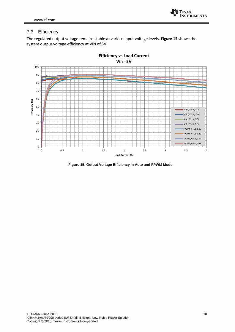
7.3 Efficiency
The regulated output voltage remains stable at various input voltage levels. Figure 15 shows the system output voltage efficiency at VIN of 5V
Figure 15: Output Voltage Efficiency in Auto and FPWM Mode
0
10
20
30
40
50
60
70
80
90
100
0 0.5 1 1.5 2 2.5 3 3.5 4
Effi
cien
cy (
%)
Load Current (A)
Efficiency vs Load Current Vin =5V
Auto_Vout_1.0V
Auto_Vout_1.2V
Auto_Vout_1.5V
Auto_Vout_1.8V
FPWM_Vout_1.0V
FPWM_Vout_1.2V
FPWM_Vout_1.5V
FPWM_Vout_1.8V

www.ti.com
TIDUA66 - June 2015 19 Xilinx® Zynq®7000 series 5W Small, Efficient, Low-Noise Power Solution Copyright © 2015, Texas Instruments Incorporated
7.4 Ripple Voltage
The output voltage ripple was measured on the output of the Buck regulator as this is critical requirement for the FPGA core voltage.
Figure 16: Ripple Voltage at Vout =1.0V

www.ti.com
TIDUA66 - June 2015 20 Xilinx® Zynq®7000 series 5W Small, Efficient, Low-Noise Power Solution Copyright © 2015, Texas Instruments Incorporated
7.5 Voltage Output accuracy
Figure 17 is a graphical representation of the computational results of the output voltage vs the load current to show that output voltage variation is within the 2% of the nominal expected voltage. The data shown below is in Forced PWM mode.
Figure 17: Output voltage vs load current
0.96
0.97
0.98
0.99
1
1.01
1.02
1.03
1.04
0 0.5 1 1.5 2 2.5 3 3.5 4
Ou
tpu
t V
olt
age
(V)
Load Current (A)
Output Voltage Regulation Vout =1.0V Vin = 5.0V

www.ti.com
TIDUA66 - June 2015 21 Xilinx® Zynq®7000 series 5W Small, Efficient, Low-Noise Power Solution Copyright © 2015, Texas Instruments Incorporated
7.6 Load Transients
Figure 18 shows the load transient capability of the LP8758 with Vout of 1V and load current switching up to 1.5A with 1A/µsec. In addition Figure 19 shows the load transient capability of the LP8758 with Vout of 1.8V and load current switching up to 300mA with 1A/µsec. The load transients can be improved with adding Point of Load (PoL) capacitors and for this experiment we have 22uF capacitors as PoL caps.
Figure 18: Load Transient for VOUT =1.0V with 1A/µsec
ILOAD
VOUT
Coupled)

www.ti.com
TIDUA66 - June 2015 22 Xilinx® Zynq®7000 series 5W Small, Efficient, Low-Noise Power Solution Copyright © 2015, Texas Instruments Incorporated
Figure 19: Load Transient for VOUT =1.8V with 1A/µsec
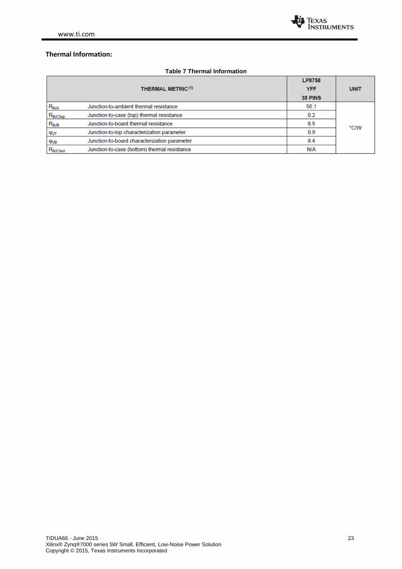
7.7 Thermal Image
Figure 20. shows thermal image of the LP8758 under full load operation at 28C ambient temperature. In addition Table 7 shows the thermal resistance for the LP8758 package on the JEDEC standard board. ) For more information about traditional and new thermal metrics, see the IC Package Thermal Metrics application report, SPRA953
Figure 20 : Thermal measurement on LP8758 EVM
VOUT
Coupled)
ILOAD
www.ti.com
TIDUA66 - June 2015 23 Xilinx® Zynq®7000 series 5W Small, Efficient, Low-Noise Power Solution Copyright © 2015, Texas Instruments Incorporated
Thermal Information:
Table 7 Thermal Information

www.ti.com
TIDUA66 - June 2015 24 Xilinx® Zynq®7000 series 5W Small, Efficient, Low-Noise Power Solution Copyright © 2015, Texas Instruments Incorporated
8 Design Files
8.1 Schematics
To download the Schematics, see the design files at http://www.ti.com/tool/TIDA-00574
Figure 3: TIDA-00574 Schematic
.

www.ti.com
TIDUA66 - June 2015 25 Xilinx® Zynq®7000 series 5W Small, Efficient, Low-Noise Power Solution Copyright © 2015, Texas Instruments Incorporated
8.2 Bill of Materials
To download the Bill of Materials, see the design files at http://www.ti.com/tool/TIDA-00574
9 Gerber Files To download the Layout Prints, see the design files at http://www.ti.com/tool/TIDA-00574
9.1 Layout Prints
To download the Layout Prints, see the design files at http://www.ti.com/tool/TIDA-00574
10 Terminology TI Glossary: SLYZ022 This glossary lists and explains terms, acronyms, and definitions
11 About the Author Chintan Parekh Is an Applications Engineer at Texas Instruments; he brings to this role experience in system-level analog, mixed-signal, and power management design.

IMPORTANT NOTICE FOR TI REFERENCE DESIGNS
Texas Instruments Incorporated ("TI") reference designs are solely intended to assist designers (“Buyers”) who are developing systems thatincorporate TI semiconductor products (also referred to herein as “components”). Buyer understands and agrees that Buyer remainsresponsible for using its independent analysis, evaluation and judgment in designing Buyer’s systems and products.TI reference designs have been created using standard laboratory conditions and engineering practices. TI has not conducted anytesting other than that specifically described in the published documentation for a particular reference design. TI may makecorrections, enhancements, improvements and other changes to its reference designs.Buyers are authorized to use TI reference designs with the TI component(s) identified in each particular reference design and to modify thereference design in the development of their end products. HOWEVER, NO OTHER LICENSE, EXPRESS OR IMPLIED, BY ESTOPPELOR OTHERWISE TO ANY OTHER TI INTELLECTUAL PROPERTY RIGHT, AND NO LICENSE TO ANY THIRD PARTY TECHNOLOGYOR INTELLECTUAL PROPERTY RIGHT, IS GRANTED HEREIN, including but not limited to any patent right, copyright, mask work right,or other intellectual property right relating to any combination, machine, or process in which TI components or services are used.Information published by TI regarding third-party products or services does not constitute a license to use such products or services, or awarranty or endorsement thereof. Use of such information may require a license from a third party under the patents or other intellectualproperty of the third party, or a license from TI under the patents or other intellectual property of TI.TI REFERENCE DESIGNS ARE PROVIDED "AS IS". TI MAKES NO WARRANTIES OR REPRESENTATIONS WITH REGARD TO THEREFERENCE DESIGNS OR USE OF THE REFERENCE DESIGNS, EXPRESS, IMPLIED OR STATUTORY, INCLUDING ACCURACY ORCOMPLETENESS. TI DISCLAIMS ANY WARRANTY OF TITLE AND ANY IMPLIED WARRANTIES OF MERCHANTABILITY, FITNESSFOR A PARTICULAR PURPOSE, QUIET ENJOYMENT, QUIET POSSESSION, AND NON-INFRINGEMENT OF ANY THIRD PARTYINTELLECTUAL PROPERTY RIGHTS WITH REGARD TO TI REFERENCE DESIGNS OR USE THEREOF. TI SHALL NOT BE LIABLEFOR AND SHALL NOT DEFEND OR INDEMNIFY BUYERS AGAINST ANY THIRD PARTY INFRINGEMENT CLAIM THAT RELATES TOOR IS BASED ON A COMBINATION OF COMPONENTS PROVIDED IN A TI REFERENCE DESIGN. IN NO EVENT SHALL TI BELIABLE FOR ANY ACTUAL, SPECIAL, INCIDENTAL, CONSEQUENTIAL OR INDIRECT DAMAGES, HOWEVER CAUSED, ON ANYTHEORY OF LIABILITY AND WHETHER OR NOT TI HAS BEEN ADVISED OF THE POSSIBILITY OF SUCH DAMAGES, ARISING INANY WAY OUT OF TI REFERENCE DESIGNS OR BUYER’S USE OF TI REFERENCE DESIGNS.TI reserves the right to make corrections, enhancements, improvements and other changes to its semiconductor products and services perJESD46, latest issue, and to discontinue any product or service per JESD48, latest issue. Buyers should obtain the latest relevantinformation before placing orders and should verify that such information is current and complete. All semiconductor products are soldsubject to TI’s terms and conditions of sale supplied at the time of order acknowledgment.TI warrants performance of its components to the specifications applicable at the time of sale, in accordance with the warranty in TI’s termsand conditions of sale of semiconductor products. Testing and other quality control techniques for TI components are used to the extent TIdeems necessary to support this warranty. Except where mandated by applicable law, testing of all parameters of each component is notnecessarily performed.TI assumes no liability for applications assistance or the design of Buyers’ products. Buyers are responsible for their products andapplications using TI components. To minimize the risks associated with Buyers’ products and applications, Buyers should provideadequate design and operating safeguards.Reproduction of significant portions of TI information in TI data books, data sheets or reference designs is permissible only if reproduction iswithout alteration and is accompanied by all associated warranties, conditions, limitations, and notices. TI is not responsible or liable forsuch altered documentation. Information of third parties may be subject to additional restrictions.Buyer acknowledges and agrees that it is solely responsible for compliance with all legal, regulatory and safety-related requirementsconcerning its products, and any use of TI components in its applications, notwithstanding any applications-related information or supportthat may be provided by TI. Buyer represents and agrees that it has all the necessary expertise to create and implement safeguards thatanticipate dangerous failures, monitor failures and their consequences, lessen the likelihood of dangerous failures and take appropriateremedial actions. Buyer will fully indemnify TI and its representatives against any damages arising out of the use of any TI components inBuyer’s safety-critical applications.In some cases, TI components may be promoted specifically to facilitate safety-related applications. With such components, TI’s goal is tohelp enable customers to design and create their own end-product solutions that meet applicable functional safety standards andrequirements. Nonetheless, such components are subject to these terms.No TI components are authorized for use in FDA Class III (or similar life-critical medical equipment) unless authorized officers of the partieshave executed an agreement specifically governing such use.Only those TI components that TI has specifically designated as military grade or “enhanced plastic” are designed and intended for use inmilitary/aerospace applications or environments. Buyer acknowledges and agrees that any military or aerospace use of TI components thathave not been so designated is solely at Buyer's risk, and Buyer is solely responsible for compliance with all legal and regulatoryrequirements in connection with such use.TI has specifically designated certain components as meeting ISO/TS16949 requirements, mainly for automotive use. In any case of use ofnon-designated products, TI will not be responsible for any failure to meet ISO/TS16949.IMPORTANT NOTICE
Mailing Address: Texas Instruments, Post Office Box 655303, Dallas, Texas 75265Copyright © 2015, Texas Instruments Incorporated