Embed Size (px)
Citation preview

XAPP1113 (v1.0) November 21, 2008 www.xilinx.com 1
© 2008 Xilinx, Inc. All rights reserved. XILINX, the Xilinx logo, and other designated brands included herein are trademarks of Xilinx, Inc. All other trademarks are the property of their respective owners.
Summary Digital Up Converters (DUC) and Digital Down Converters (DDC) are key components of RF systems in communications, sensing, and imaging. This application note demonstrates how efficient DUC/DDC implementations can be created by leveraging Xilinx® DSP tools and IP portfolio for increased productivity and reduced development time. While previous application notes [Ref 1] have provided examples of DUC and DDC implementation in wideband communications systems, this document concentrates on narrowband systems and the building block components available to meet the particular requirements of such designs.
Step-by-step guidance is provided on how to perform simulation of narrowband DUC/DDC systems in MATLAB®, how to map functions onto building blocks and IP cores for Xilinx® FPGAs in System Generator software, and how to verify the implementation against the simulation model. Two examples are provided: a multi-carrier GSM system (both DUC and DDC) and a multi-channel MRI receiver (DDC only). The examples provide a guide and template for implementation of customer-specific solutions and, in many cases, may be readily adapted to customers’ own application systems. Advantages and limitations of the approaches and methods employed are identified such that the reader can consider these in their own system context.
Introduction In terms of signal processing, narrowband systems are generally characterized by the fact that the bandwidth of the signal of interest is significantly less than the sampled bandwidth; that is, a narrow band of frequencies must be selected and filtered out from a much wider spectral window in which the signal might occur. This means that large sample rate changes (in the hundreds or even thousands) must be undertaken to efficiently process the signal for either transmission or reception. Examples of such systems include: communications systems, where several narrow channels must be recovered from a wider transmission band, or medical imaging systems, such as MRI, where the detected waveforms occur in a narrow range of frequencies at varying points within a wider spectrum, as well as many other systems that fall within this grouping.
[Ref 1] deals with wideband systems, providing guidance on how to select an appropriate cascaded FIR structure to meet the sample rate change requirements of wireless base stations. When the desired sample rate change is 32 or more, it is advisable to consider the use of CIC filters. CIC filters are an alternative class of filters to FIR filters, and they are well-suited to large sample rate changes, as they can be implemented efficiently in digital circuits. They are often used in conjunction with small Finite Impulse Response (FIR) filters to implement the filter chain of up- and down-converters in narrowband systems. While such converters have been implemented often for many years in both Application Specific Standard Products (ASSPs) and FPGAs, these have generally provided only single-channel solutions, or multiple instances thereof. The latest high-density FPGA families with advanced architectures, in combination with efficient IP cores and effective design tools, provide the capability to handle many channels simultaneously. This application note demonstrates how to implement such designs.
Highlights:
• DUC and DDC design files for 4-carrier GSM, targeting Virtex®-5 FPGAs
Application Note: Virtex-5 Family
XAPP1113 (v1.0) November 21, 2008
Designing Efficient Digital Up and Down Converters for Narrowband SystemsAuthor: Stephen Creaney and Igor Kostarnov
R

Introduction
XAPP1113 (v1.0) November 21, 2008 www.xilinx.com 2
R
• DDC design files for multi-channel MRI, targeting both Virtex-5 and Spartan®-DSP FPGAs
• Designed using class-leading Xilinx® DSP IP portfolio
• Design flow for System Generator software for both designs
• Automatic scripted generation of implementation schematics based on system parameters for the MRI design.
System Requirements
This application note was designed using MATLAB version 7.3.0 (R2006b) and the unified release of the Xilinx® ISE® and DSP tools (System Generator) version 10.1.
Additional Reading
It is recommended that the reader be familiar with data sheets for the Xilinx® Cascaded Integrator Comb (CIC) Compiler [Ref 2], Direct Digital Synthesizer (DDS) Compiler [Ref 3], and Finite Impulse Response (FIR) Compiler [Ref 4] IP cores.
A reasonable level of familiarity with Xilinx tools, in general, and System Generator software, in particular, is assumed. Further information can be found in the software manuals [Ref 5] provided on the Xilinx website.
Acronyms and Abbreviations
Table 1: Acronyms and Abbreviations
3GPP 3rd Generation Partnership Project
ADC Analog-to-Digital Converter
AGC Automatic Gain Correction
ASIC Application Specific Integrated Circuit
ASSP Application Specific Standard Product
Block RAM Block Random Access Memory (Xilinx device resource)
BS Base Station
BT Bandwidth-Time
BTS Base Transceiver Station
CapEx Capital Expenditure
CFR Crest Factor Reduction
CIC Cascaded Integrator Comb
CFIR Compensation Finite Impulse Response Filter
DAC Digital-to-Analog Converter
dB Decibel
DDC Digital Down Converter
DDS Direct Digital Synthesizer
DFE Digital Front End
DPD Digital Pre-Distortion
DSP Digital Signal Processing/Processor
DUC Digital Up Converter
EDGE Enhanced Data rates for GSM Evolution
EDGE2 or e-EDGE Evolved EDGE
FPGA Field Programmable Gate Array
FID Free-Induction Decay
FIR Finite Impulse Response

Introduction
XAPP1113 (v1.0) November 21, 2008 www.xilinx.com 3
R
GMSK Gaussian Minimum Shift Keying
GSM Global System for Mobile Communication, originated from Groupe Spécial Mobile
GUI Graphical User Interface
HDL Hardware Description Language
HOR Hardware Over-sampling Rate
IF Intermediate Frequency
IMD Inter-Modulation Distortion
ISI Inter-Symbol Interference
kbaud Kilo-baud (1,000 symbols per second)
ksps Kilo-samples per second (1,000 samples per second)
LSB Least Significant Bit(s)
LPF Low Pass Filter
LUT Look-Up Table
MAC Multiply-Accumulate
MRI Magnetic Resonance Imaging
MSB Most Significant Bit(s)
MSK Minimum Shift Keying
Msps Mega-samples per second (1,000,000 samples per second)
NCO Numerically Controlled Oscillator
OpEx Operation Expenditures
PA Power Amplifier
PAPR Peak-to-Average Power Ratio
PAR Place and Route
PFIR Pulse-Shaping Finite Impulse Response (Filter)
PSD Power Spectral Density
RMS Root Mean Square
RRC Root-Raised Cosine
RRH Remote Radio Head
SFDR Spurious-Free Dynamic Range
SNR Signal-to-Noise Ratio
TDDM Time Division De-Multiplex
TDM Time Division Multiplex
XST Xilinx Synthesis Technology
Table 1: Acronyms and Abbreviations (Cont’d)

Contents
XAPP1113 (v1.0) November 21, 2008 www.xilinx.com 4
R
Contents Summary . . . . . . . . . . . . . . . . . . . . . . . . . . . . . . . . . . . . . . . . . . . . . . . . . . . . . . . . . . . . . . . . . . . . . . . . 1Introduction. . . . . . . . . . . . . . . . . . . . . . . . . . . . . . . . . . . . . . . . . . . . . . . . . . . . . . . . . . . . . . . . . . . . . . . 1
System Requirements . . . . . . . . . . . . . . . . . . . . . . . . . . . . . . . . . . . . . . . . . . . . . . . . . . . . . . . . 2Additional Reading . . . . . . . . . . . . . . . . . . . . . . . . . . . . . . . . . . . . . . . . . . . . . . . . . . . . . . . . . . . 2Acronyms and Abbreviations . . . . . . . . . . . . . . . . . . . . . . . . . . . . . . . . . . . . . . . . . . . . . . . . . . . 2Contents . . . . . . . . . . . . . . . . . . . . . . . . . . . . . . . . . . . . . . . . . . . . . . . . . . . . . . . . . . . . . . . . . . . 4Figures . . . . . . . . . . . . . . . . . . . . . . . . . . . . . . . . . . . . . . . . . . . . . . . . . . . . . . . . . . . . . . . . . . . . 5Tables. . . . . . . . . . . . . . . . . . . . . . . . . . . . . . . . . . . . . . . . . . . . . . . . . . . . . . . . . . . . . . . . . . . . . 6
Overview . . . . . . . . . . . . . . . . . . . . . . . . . . . . . . . . . . . . . . . . . . . . . . . . . . . . . . . . . . . . . . . . . . . . . . . . 7Digital Up Converters . . . . . . . . . . . . . . . . . . . . . . . . . . . . . . . . . . . . . . . . . . . . . . . . . . . . . . . . . 7Digital Down Converters (DDC) . . . . . . . . . . . . . . . . . . . . . . . . . . . . . . . . . . . . . . . . . . . . . . . . . 7Building Blocks for Narrowband DUC/DDC Systems. . . . . . . . . . . . . . . . . . . . . . . . . . . . . . . . . 8
Mixers. . . . . . . . . . . . . . . . . . . . . . . . . . . . . . . . . . . . . . . . . . . . . . . . . . . . . . . . . . . . . . . . . 8Direct Digital Synthesizers . . . . . . . . . . . . . . . . . . . . . . . . . . . . . . . . . . . . . . . . . . . . . . . . . 11Finite Impulse Response Filters. . . . . . . . . . . . . . . . . . . . . . . . . . . . . . . . . . . . . . . . . . . . . 14CIC Filters . . . . . . . . . . . . . . . . . . . . . . . . . . . . . . . . . . . . . . . . . . . . . . . . . . . . . . . . . . . . . 16
Critical Design Parameters for DUC/DDC Systems . . . . . . . . . . . . . . . . . . . . . . . . . . . . . . . . . . 21Total Rate Change . . . . . . . . . . . . . . . . . . . . . . . . . . . . . . . . . . . . . . . . . . . . . . . . . . . . . . . 21Clock Rate . . . . . . . . . . . . . . . . . . . . . . . . . . . . . . . . . . . . . . . . . . . . . . . . . . . . . . . . . . . . . 21Number of Carriers (or Subcarriers). . . . . . . . . . . . . . . . . . . . . . . . . . . . . . . . . . . . . . . . . . 21Number of Channels . . . . . . . . . . . . . . . . . . . . . . . . . . . . . . . . . . . . . . . . . . . . . . . . . . . . . 21Modulation Scheme . . . . . . . . . . . . . . . . . . . . . . . . . . . . . . . . . . . . . . . . . . . . . . . . . . . . . . 22Supported Standards . . . . . . . . . . . . . . . . . . . . . . . . . . . . . . . . . . . . . . . . . . . . . . . . . . . . . 22
Application Example: Multi-Carrier GSM (MC-GSM) . . . . . . . . . . . . . . . . . . . . . . . . . . . . . . . . . . . . . . . 22Digital Up-Converter. . . . . . . . . . . . . . . . . . . . . . . . . . . . . . . . . . . . . . . . . . . . . . . . . . . . . . . . . . 23
Performance Requirements . . . . . . . . . . . . . . . . . . . . . . . . . . . . . . . . . . . . . . . . . . . . . . . . 23DUC Input . . . . . . . . . . . . . . . . . . . . . . . . . . . . . . . . . . . . . . . . . . . . . . . . . . . . . . . . . . . . . 25DUC Filter Design . . . . . . . . . . . . . . . . . . . . . . . . . . . . . . . . . . . . . . . . . . . . . . . . . . . . . . . 28Frequency Translation . . . . . . . . . . . . . . . . . . . . . . . . . . . . . . . . . . . . . . . . . . . . . . . . . . . . 33DUC Modeling and Performance . . . . . . . . . . . . . . . . . . . . . . . . . . . . . . . . . . . . . . . . . . . . 34DUC Implementation . . . . . . . . . . . . . . . . . . . . . . . . . . . . . . . . . . . . . . . . . . . . . . . . . . . . . 37Synthesis . . . . . . . . . . . . . . . . . . . . . . . . . . . . . . . . . . . . . . . . . . . . . . . . . . . . . . . . . . . . . . 40DUC Verification. . . . . . . . . . . . . . . . . . . . . . . . . . . . . . . . . . . . . . . . . . . . . . . . . . . . . . . . . 41DUC Resource Utilization . . . . . . . . . . . . . . . . . . . . . . . . . . . . . . . . . . . . . . . . . . . . . . . . . 43DUC Power Consumption . . . . . . . . . . . . . . . . . . . . . . . . . . . . . . . . . . . . . . . . . . . . . . . . . 43Limitations of CIC-based DUC Implementation . . . . . . . . . . . . . . . . . . . . . . . . . . . . . . . . . 44
Digital Down-Converter . . . . . . . . . . . . . . . . . . . . . . . . . . . . . . . . . . . . . . . . . . . . . . . . . . . . . . . 45Performance Requirements . . . . . . . . . . . . . . . . . . . . . . . . . . . . . . . . . . . . . . . . . . . . . . . . 45DDC Input . . . . . . . . . . . . . . . . . . . . . . . . . . . . . . . . . . . . . . . . . . . . . . . . . . . . . . . . . . . . . 46Frequency Translation . . . . . . . . . . . . . . . . . . . . . . . . . . . . . . . . . . . . . . . . . . . . . . . . . . . . 46DDC Filter Design . . . . . . . . . . . . . . . . . . . . . . . . . . . . . . . . . . . . . . . . . . . . . . . . . . . . . . . 47DDC Modeling and Performance . . . . . . . . . . . . . . . . . . . . . . . . . . . . . . . . . . . . . . . . . . . . 51DDC Implementation . . . . . . . . . . . . . . . . . . . . . . . . . . . . . . . . . . . . . . . . . . . . . . . . . . . . . 55Synthesis . . . . . . . . . . . . . . . . . . . . . . . . . . . . . . . . . . . . . . . . . . . . . . . . . . . . . . . . . . . . . . 57DDC Verification. . . . . . . . . . . . . . . . . . . . . . . . . . . . . . . . . . . . . . . . . . . . . . . . . . . . . . . . . 58DDC Resource Utilization . . . . . . . . . . . . . . . . . . . . . . . . . . . . . . . . . . . . . . . . . . . . . . . . . 61Limitations of CIC-Based DDC Implementation . . . . . . . . . . . . . . . . . . . . . . . . . . . . . . . . . 62
Application Example: Multi-Channel MRI Receiver . . . . . . . . . . . . . . . . . . . . . . . . . . . . . . . . . . . . . . . . 62Design Files . . . . . . . . . . . . . . . . . . . . . . . . . . . . . . . . . . . . . . . . . . . . . . . . . . . . . . . . . . . . . . . . 62Application Overview . . . . . . . . . . . . . . . . . . . . . . . . . . . . . . . . . . . . . . . . . . . . . . . . . . . . . . . . . 63Digital Down-Converter . . . . . . . . . . . . . . . . . . . . . . . . . . . . . . . . . . . . . . . . . . . . . . . . . . . . . . . 64
Architectural Consideration . . . . . . . . . . . . . . . . . . . . . . . . . . . . . . . . . . . . . . . . . . . . . . . . 64Performance Requirements . . . . . . . . . . . . . . . . . . . . . . . . . . . . . . . . . . . . . . . . . . . . . . . . 65Input . . . . . . . . . . . . . . . . . . . . . . . . . . . . . . . . . . . . . . . . . . . . . . . . . . . . . . . . . . . . . . . . . . 66Modeling. . . . . . . . . . . . . . . . . . . . . . . . . . . . . . . . . . . . . . . . . . . . . . . . . . . . . . . . . . . . . . . 66Filter Design . . . . . . . . . . . . . . . . . . . . . . . . . . . . . . . . . . . . . . . . . . . . . . . . . . . . . . . . . . . . 67Frequency Translation . . . . . . . . . . . . . . . . . . . . . . . . . . . . . . . . . . . . . . . . . . . . . . . . . . . . 70Implementation. . . . . . . . . . . . . . . . . . . . . . . . . . . . . . . . . . . . . . . . . . . . . . . . . . . . . . . . . . 70Synthesis . . . . . . . . . . . . . . . . . . . . . . . . . . . . . . . . . . . . . . . . . . . . . . . . . . . . . . . . . . . . . . 72Verification . . . . . . . . . . . . . . . . . . . . . . . . . . . . . . . . . . . . . . . . . . . . . . . . . . . . . . . . . . . . . 72Resource Utilization . . . . . . . . . . . . . . . . . . . . . . . . . . . . . . . . . . . . . . . . . . . . . . . . . . . . . . 73Individual Channel Implementation . . . . . . . . . . . . . . . . . . . . . . . . . . . . . . . . . . . . . . . . . . 73Power Consumption. . . . . . . . . . . . . . . . . . . . . . . . . . . . . . . . . . . . . . . . . . . . . . . . . . . . . . 75
Conclusion . . . . . . . . . . . . . . . . . . . . . . . . . . . . . . . . . . . . . . . . . . . . . . . . . . . . . . . . . . . . . . . . . . . . . . . 76References . . . . . . . . . . . . . . . . . . . . . . . . . . . . . . . . . . . . . . . . . . . . . . . . . . . . . . . . . . . . . . . . . . . . . . . 76Revision History . . . . . . . . . . . . . . . . . . . . . . . . . . . . . . . . . . . . . . . . . . . . . . . . . . . . . . . . . . . . . . . . . . . 78Notice of Disclaimer . . . . . . . . . . . . . . . . . . . . . . . . . . . . . . . . . . . . . . . . . . . . . . . . . . . . . . . . . . . . . . . . 78

Figures
XAPP1113 (v1.0) November 21, 2008 www.xilinx.com 5
R
Figures Figure 1. Generic DUC architecture . . . . . . . . . . . . . . . . . . . . . . . . . . . . . . . . . . . . . . . . . . . . . . . . . . . . . . . . . . 7Figure 2. Generic DDC Architecture. . . . . . . . . . . . . . . . . . . . . . . . . . . . . . . . . . . . . . . . . . . . . . . . . . . . . . . . . . 8Figure 3. Virtex-5 FPGA DSP48E Block Diagram . . . . . . . . . . . . . . . . . . . . . . . . . . . . . . . . . . . . . . . . . . . . . . . 10Figure 4. Two-Stage Mixing of Multi-Carrier Signals . . . . . . . . . . . . . . . . . . . . . . . . . . . . . . . . . . . . . . . . . . . . . 11Figure 5. Block Diagram of the DDS Compiler Block . . . . . . . . . . . . . . . . . . . . . . . . . . . . . . . . . . . . . . . . . . . . . 12Figure 6. SFDR Performance of Taylor Series Corrected DDS with Swept Frequency . . . . . . . . . . . . . . . . . . . 12Figure 7. DDS Compiler Token and GUI in System Generator . . . . . . . . . . . . . . . . . . . . . . . . . . . . . . . . . . . . . 13Figure 8. Single MAC FIR Filter Implementation . . . . . . . . . . . . . . . . . . . . . . . . . . . . . . . . . . . . . . . . . . . . . . . . 14Figure 9. FIR Compiler Token and GUI in System Generator . . . . . . . . . . . . . . . . . . . . . . . . . . . . . . . . . . . . . . 15Figure 10. CIC Component Stages . . . . . . . . . . . . . . . . . . . . . . . . . . . . . . . . . . . . . . . . . . . . . . . . . . . . . . . . . . 16Figure 11. CIC Decimation and Interpolation Structures . . . . . . . . . . . . . . . . . . . . . . . . . . . . . . . . . . . . . . . . . . 17Figure 12. Example CIC Magnitude Response Plot . . . . . . . . . . . . . . . . . . . . . . . . . . . . . . . . . . . . . . . . . . . . . . 18Figure 13. CIC passband Aliasing . . . . . . . . . . . . . . . . . . . . . . . . . . . . . . . . . . . . . . . . . . . . . . . . . . . . . . . . . . . 18Figure 14. CIC Passband Imaging . . . . . . . . . . . . . . . . . . . . . . . . . . . . . . . . . . . . . . . . . . . . . . . . . . . . . . . . . . . 19Figure 15. Illustration of Passband Droop Compensation . . . . . . . . . . . . . . . . . . . . . . . . . . . . . . . . . . . . . . . . . 19Figure 16. CIC Compiler Token and GUI in System Generator . . . . . . . . . . . . . . . . . . . . . . . . . . . . . . . . . . . . . 20Figure 17. GSM Transmission Spectral Mask . . . . . . . . . . . . . . . . . . . . . . . . . . . . . . . . . . . . . . . . . . . . . . . . . . 25Figure 18. Spectrum of GMSK Modulated Signal. . . . . . . . . . . . . . . . . . . . . . . . . . . . . . . . . . . . . . . . . . . . . . . . 26Figure 19. Scatter Plot of GMSK Modulated Data . . . . . . . . . . . . . . . . . . . . . . . . . . . . . . . . . . . . . . . . . . . . . . . 26Figure 20. Eye Diagram of GMSK Modulated Data, Illustrating Frequency Trajectories . . . . . . . . . . . . . . . . . . 27Figure 21. Spectral Comparison of GSM and EDGE . . . . . . . . . . . . . . . . . . . . . . . . . . . . . . . . . . . . . . . . . . . . . 28Figure 22. 3-Stage CIC-Based DUC Filtering. . . . . . . . . . . . . . . . . . . . . . . . . . . . . . . . . . . . . . . . . . . . . . . . . . . 28Figure 23. Magnitude Response of CIC Filter . . . . . . . . . . . . . . . . . . . . . . . . . . . . . . . . . . . . . . . . . . . . . . . . . . 30Figure 24. Magnitude Response of CFIR Filter . . . . . . . . . . . . . . . . . . . . . . . . . . . . . . . . . . . . . . . . . . . . . . . . . 31Figure 25. Passband Zoom Overlay of CIC, CFIR, and Combined Frequency Responses. . . . . . . . . . . . . . . . 32Figure 26. Overall DUC Filter Response . . . . . . . . . . . . . . . . . . . . . . . . . . . . . . . . . . . . . . . . . . . . . . . . . . . . . . 32Figure 27. Overlay of DUC Filter Responses . . . . . . . . . . . . . . . . . . . . . . . . . . . . . . . . . . . . . . . . . . . . . . . . . . . 33Figure 28. CFIR Output Power Spectral Density . . . . . . . . . . . . . . . . . . . . . . . . . . . . . . . . . . . . . . . . . . . . . . . . 35Figure 29. CIC Filter Output Power Spectral Density . . . . . . . . . . . . . . . . . . . . . . . . . . . . . . . . . . . . . . . . . . . . . 35Figure 30. PSD of DDS Generated Carriers vs. Ideal Sinusoidal Carriers . . . . . . . . . . . . . . . . . . . . . . . . . . . . . 36Figure 31. Single Carrier Mixed with -900 kHz Carrier . . . . . . . . . . . . . . . . . . . . . . . . . . . . . . . . . . . . . . . . . . . . 36Figure 32. Power Spectral Density for Multi-Carrier GSM Waveform . . . . . . . . . . . . . . . . . . . . . . . . . . . . . . . . 37Figure 33. Top-Level Block Diagram for MC-GSM DUC Implementation . . . . . . . . . . . . . . . . . . . . . . . . . . . . . 37Figure 34. Virtex-5 Mixer FPGA Implementation in System Generator Software. . . . . . . . . . . . . . . . . . . . . . . . 39Figure 35. Complex Mixer Implementation with Cascaded DSP48 Slices . . . . . . . . . . . . . . . . . . . . . . . . . . . . . 40Figure 36. Comparative Analysis of CFIR Output Results – Exact Match . . . . . . . . . . . . . . . . . . . . . . . . . . . . . 41Figure 37. Comparative Analysis of Up-Mixed Multi-Carrier Signal – Exact Match . . . . . . . . . . . . . . . . . . . . . . 42Figure 38. Zoom of Up-Mixed Multi-Carrier Signal Comparison. . . . . . . . . . . . . . . . . . . . . . . . . . . . . . . . . . . . . 42Figure 39. Relaxed GSM Reception Spectral Mask . . . . . . . . . . . . . . . . . . . . . . . . . . . . . . . . . . . . . . . . . . . . . . 46Figure 40. 3-Stage CIC-Based DDC Filtering. . . . . . . . . . . . . . . . . . . . . . . . . . . . . . . . . . . . . . . . . . . . . . . . . . . 47Figure 41. Magnitude Response of CIC Filter . . . . . . . . . . . . . . . . . . . . . . . . . . . . . . . . . . . . . . . . . . . . . . . . . . 48Figure 42. Magnitude Response of CFIR Filter . . . . . . . . . . . . . . . . . . . . . . . . . . . . . . . . . . . . . . . . . . . . . . . . . 49Figure 43. Passband Zoom Overlay of CIC, CFIR, and Combined Frequency Responses. . . . . . . . . . . . . . . . 49Figure 44. Magnitude Response of PFIR Filter . . . . . . . . . . . . . . . . . . . . . . . . . . . . . . . . . . . . . . . . . . . . . . . . . 50Figure 45. Overall DUC Filter Response . . . . . . . . . . . . . . . . . . . . . . . . . . . . . . . . . . . . . . . . . . . . . . . . . . . . . . 50Figure 46. Overlay of DDC Filter Responses . . . . . . . . . . . . . . . . . . . . . . . . . . . . . . . . . . . . . . . . . . . . . . . . . . . 51Figure 47. DDC Input Signal. . . . . . . . . . . . . . . . . . . . . . . . . . . . . . . . . . . . . . . . . . . . . . . . . . . . . . . . . . . . . . . . 52Figure 48. PSD of DDS Generated Carriers vs. Ideal Sinusoidal Carriers . . . . . . . . . . . . . . . . . . . . . . . . . . . . . 52Figure 49. Received Signal Spectra Shifted by -900 kHz and +300 kHz Carriers . . . . . . . . . . . . . . . . . . . . . . . 53Figure 50. CIC Filter Output Power Spectral Density . . . . . . . . . . . . . . . . . . . . . . . . . . . . . . . . . . . . . . . . . . . . . 53Figure 51. CFIR Output Power Spectral Density . . . . . . . . . . . . . . . . . . . . . . . . . . . . . . . . . . . . . . . . . . . . . . . . 54Figure 52. PFIR Output Power Spectral Density . . . . . . . . . . . . . . . . . . . . . . . . . . . . . . . . . . . . . . . . . . . . . . . . 54Figure 53. Top-Level Block Diagram for MC-GSM DDC Implementation . . . . . . . . . . . . . . . . . . . . . . . . . . . . . 55Figure 54. Virtex-5 FPGA Mixer Implementation in System Generator . . . . . . . . . . . . . . . . . . . . . . . . . . . . . . . 56Figure 55. Comparative Analysis of Down-Mixed Signal, Channel 1 . . . . . . . . . . . . . . . . . . . . . . . . . . . . . . . . . 58Figure 56. Zoom of Down-Mixed Signal Comparison, Channel 1 . . . . . . . . . . . . . . . . . . . . . . . . . . . . . . . . . . . 58Figure 57. Comparative Analysis of CIC Output Results . . . . . . . . . . . . . . . . . . . . . . . . . . . . . . . . . . . . . . . . . . 59Figure 58. Comparative Analysis of CFIR Output Results . . . . . . . . . . . . . . . . . . . . . . . . . . . . . . . . . . . . . . . . . 59Figure 59. Comparative Analysis of PFIR Output Results . . . . . . . . . . . . . . . . . . . . . . . . . . . . . . . . . . . . . . . . . 60Figure 60. MRI Scanner Equipment . . . . . . . . . . . . . . . . . . . . . . . . . . . . . . . . . . . . . . . . . . . . . . . . . . . . . . . . . . 63Figure 61. MRI Pre-amplifier and Converter Context . . . . . . . . . . . . . . . . . . . . . . . . . . . . . . . . . . . . . . . . . . . . . 64Figure 62. MRI DDC CIC Frequency Response. . . . . . . . . . . . . . . . . . . . . . . . . . . . . . . . . . . . . . . . . . . . . . . . . 67Figure 63. CFIR Frequency Response. . . . . . . . . . . . . . . . . . . . . . . . . . . . . . . . . . . . . . . . . . . . . . . . . . . . . . . . 68Figure 64. Combined Frequency Response of Filter Cascade. . . . . . . . . . . . . . . . . . . . . . . . . . . . . . . . . . . . . . 68Figure 65. Passband Zoom of Compensated Frequency Response . . . . . . . . . . . . . . . . . . . . . . . . . . . . . . . . . 69Figure 66. Single Channel DDC for MRI . . . . . . . . . . . . . . . . . . . . . . . . . . . . . . . . . . . . . . . . . . . . . . . . . . . . . . 71Figure 67. 8-Channel DDC for MRI . . . . . . . . . . . . . . . . . . . . . . . . . . . . . . . . . . . . . . . . . . . . . . . . . . . . . . . . . . 73

Tables
XAPP1113 (v1.0) November 21, 2008 www.xilinx.com 6
R
Tables Table 1. Acronyms and Abbreviations . . . . . . . . . . . . . . . . . . . . . . . . . . . . . . . . . . . . . . . . . . . . . . . . . . . . . . . . 2Table 2. System Generator DDS Compiler Block Interface . . . . . . . . . . . . . . . . . . . . . . . . . . . . . . . . . . . . . . . . 13Table 3. System Generator FIR Compiler Block Interface . . . . . . . . . . . . . . . . . . . . . . . . . . . . . . . . . . . . . . . . . 15Table 4. System Generator CIC Compiler Block Interface . . . . . . . . . . . . . . . . . . . . . . . . . . . . . . . . . . . . . . . . . 20Table 5. Target Specification for GSM Downlink Transmit Path . . . . . . . . . . . . . . . . . . . . . . . . . . . . . . . . . . . . 23Table 6. GSM Spectral Mask Requirements for Transmission. . . . . . . . . . . . . . . . . . . . . . . . . . . . . . . . . . . . . . 24Table 7. Summary of Key Parameters to Program DDS Compiler for MC-GSM . . . . . . . . . . . . . . . . . . . . . . . . 33Table 8. Model Parameters . . . . . . . . . . . . . . . . . . . . . . . . . . . . . . . . . . . . . . . . . . . . . . . . . . . . . . . . . . . . . . . . 34Table 9. Resource Utilization of 4-Carrier GSM DUC . . . . . . . . . . . . . . . . . . . . . . . . . . . . . . . . . . . . . . . . . . . . 43Table 10. Resource Utilization of 4-Carrier GSM DUC Using DSP Slices for CI . . . . . . . . . . . . . . . . . . . . . . . . 43Table 11. Power Consumption of 4-Carrier GSM DUC Using Logic Slices for CIC . . . . . . . . . . . . . . . . . . . . . . 43Table 12. Power Consumption of 4-Carrier GSM DUC Using DSP Slices for CIC . . . . . . . . . . . . . . . . . . . . . . 43Table 13. Target Specification for GSM Uplink Receive Path . . . . . . . . . . . . . . . . . . . . . . . . . . . . . . . . . . . . . . 45Table 14. GSM Spectral Mask Requirements for Reception . . . . . . . . . . . . . . . . . . . . . . . . . . . . . . . . . . . . . . . 45Table 15. Key Parameters to Program DDS Compiler for MC-GSM . . . . . . . . . . . . . . . . . . . . . . . . . . . . . . . . . 46Table 16. Model Parameters . . . . . . . . . . . . . . . . . . . . . . . . . . . . . . . . . . . . . . . . . . . . . . . . . . . . . . . . . . . . . . . 52Table 17. Resource Utilization of 4-carrier GSM DDC . . . . . . . . . . . . . . . . . . . . . . . . . . . . . . . . . . . . . . . . . . . . 61Table 18. Resource Utilization of 4-carrier GSM DDC Using DSP Slices for CIC . . . . . . . . . . . . . . . . . . . . . . . 61Table 19. Power Consumption of 4-Carrier GSM DDC Using Logic Slices for CIC . . . . . . . . . . . . . . . . . . . . . . 61Table 20. Power Consumption of 4-carrier GSM DDC using DSP slices for CIC . . . . . . . . . . . . . . . . . . . . . . . 61Table 21. MRI example design files . . . . . . . . . . . . . . . . . . . . . . . . . . . . . . . . . . . . . . . . . . . . . . . . . . . . . . . . . . 62Table 22. Gyromagnetic Ratios for Different Nuclei . . . . . . . . . . . . . . . . . . . . . . . . . . . . . . . . . . . . . . . . . . . . . . 64Table 23. Typical DDC Requirements for MRI . . . . . . . . . . . . . . . . . . . . . . . . . . . . . . . . . . . . . . . . . . . . . . . . . . 65Table 24. MRI DDC model parameters . . . . . . . . . . . . . . . . . . . . . . . . . . . . . . . . . . . . . . . . . . . . . . . . . . . . . . . 66Table 25. Individual Channel Resource Utilization (per channel) . . . . . . . . . . . . . . . . . . . . . . . . . . . . . . . . . . . . 73Table 26. Resource Utilization for 21-Channel Implementation . . . . . . . . . . . . . . . . . . . . . . . . . . . . . . . . . . . . . 75Table 27. Power Consumption for Individual Channel Implementation (per channel) . . . . . . . . . . . . . . . . . . . . 75Table 28. Power Consumption for 21-Channel Implementation. . . . . . . . . . . . . . . . . . . . . . . . . . . . . . . . . . . . . 76

Overview
XAPP1113 (v1.0) November 21, 2008 www.xilinx.com 7
R
Overview Digital Up Converters
A Digital Up-Converter (DUC) is a key component of digital front-end (DFE) circuits for RF systems in communications, sensing, and imaging. The function of the DUC is to translate one or more channels of data from baseband to a passband signal comprising modulated carriers at a set of one or more specified radio or intermediate frequencies (RF or IF). It achieves this by performing: interpolation to increase the sample rate, filtering to provide spectral shaping and rejection of interpolation images, and mixing to shift the signal spectrum to the desired carrier frequencies. The sample rate at the input to the DUC is relatively low; for example, the symbol rate of a digital communications system, while the output is a much higher rate, generally the input sample rate to a Digital-to-Analog Converter (DAC), which converts the digital samples to an analog waveform for further analog processing and frequency conversion.
A generic architecture for a DUC is shown in Figure 1. A modulator (or other digital channel signal source) feeds into a set of filters for pulse-shaping and interpolation, and the filter output is then mixed with a vector of one or more carrier frequencies. Optionally, in advanced systems, further filtering (interpolation), RF processing (for example, Crest Factor Reduction (CFR), Digital Pre-Distortion (DPD), Modulation Correction, etc)., and frequency translation (to shift to a passband centre frequency) may be performed. Finally, the up-converted signal is converted to an analog signal for further processing and up-conversion to the RF band.
This application note covers the functions of the filters and the main mixer (indicated by the red box in Figure 1), with some reference to modulators and converters. The optional functions are discussed briefly where relevant to provide some system context.
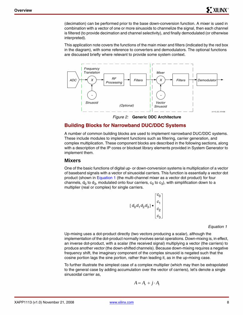
Digital Down Converters (DDC)
A Digital Down Converter (DDC) is the counterpart component to the DUC and is, therefore, equally important as a component in the same application systems. Its function is to translate a passband signal comprising one or more radio or intermediate frequency (RF or IF) carriers to one or more baseband channels for demodulation and interpretation. It achieves this by performing: mixing to shift the signal spectrum from the selected carrier frequencies to baseband, decimation to reduce the sample rate, and filtering to remove adjacent channels, minimize aliasing, and maximize the received signal-to-noise ratio (SNR). The DDC input signal has a relatively high sample rate, generally, the output sample rate of an Analog-to-Digital Converter (ADC) which samples the detected signal (often after analog frequency translation and pre-processing), while the output is a much lower rate, for example, the symbol rate of a digital communications system for demodulation.
A generic architecture for a DDC is shown in Figure 2. An ADC samples the detected analog signal and feeds into the DDC processing chain. Optionally, in advanced systems, an initial frequency translation (to shift the center frequency from passband to baseband), RF processing (for example, channel estimation and carrier recovery), and additional filtering
X-Ref Target - Figure 1
Figure 1: Generic DUC architectureX1113_01_10140808
Modulator Filters
Mixer
VectorSinusoid
Filters RFProcessing
X
~
X
~
FrequencyTranslation
Sinusoid
(Optional)
DAC
Overview
XAPP1113 (v1.0) November 21, 2008 www.xilinx.com 8
R
(decimation) can be performed prior to the base down-conversion function. A mixer is used in combination with a vector of one or more sinusoids to channelize the signal, then each channel is filtered (to provide decimation and channel selectivity), and finally demodulated (or otherwise interpreted).
This application note covers the functions of the main mixer and filters (indicated by the red box in the diagram), with some reference to converters and demodulators. The optional functions are discussed briefly where relevant to provide some system context.
Building Blocks for Narrowband DUC/DDC Systems
A number of common building blocks are used to implement narrowband DUC/DDC systems. These include modules to implement functions such as filtering, carrier generation, and complex multiplication. These component blocks are described in the following sections, along with a description of the IP cores or blockset library elements provided in System Generator to implement them.
MixersOne of the basic functions of digital up- or down-conversion systems is multiplication of a vector of baseband signals with a vector of sinusoidal carriers. This function is essentially a vector dot product (shown in Equation 1 (the multi-channel mixer as a vector dot product) for four channels, d0 to d3, modulated onto four carriers, c0 to c3), with simplification down to a multiplier (real or complex) for single carriers.
Equation 1
Up-mixing uses a dot-product directly (two vectors producing a scalar), although the implementation of the dot-product normally involves serial operations. Down-mixing is, in effect, an inverse dot-product, with a scalar (the received signal) multiplying a vector (the carriers) to produce another vector (the down-shifted channels). Because down-mixing requires a negative frequency shift, the imaginary component of the complex sinusoid is negated such that the cosine portion lags the sine portion, rather than leading it, as in the up-mixing case.
To further illustrate the simplest case of a complex multiplier (which may then be extrapolated to the general case by adding accumulation over the vector of carriers), let's denote a single sinusoidal carrier as,
X-Ref Target - Figure 2
Figure 2: Generic DDC Architecture
DemodulatorFiltersFiltersRFProcessing
(Optional)
ADC
Mixer
VectorSinusoid
X
~
X
~
FrequencyTranslation
Sinusoid
x1113_02_101408
d0d1d2d3 ][
c0
c1
c2
c3
•
r iA A j A= + ⋅

Overview
XAPP1113 (v1.0) November 21, 2008 www.xilinx.com 9
R
where
and,
and the baseband data waveform as,
where Br and Bi are the in-phase and quadrature components of the baseband signal (normally a filtered and up-sampled version of the modulator output for a DUC, or the ADC sample inputs for a DDC). The mixer output is shown in Equation 2 (Single carrier mixing (complex multiplication)):
Equation 2
Pi and Pr are defined as the real and imaginary part of the result from the complex multiplication, with each of these terms requiring two multiplications and one addition or subtraction. This sequence of operations can be implemented using the high performance XtremeDSP™ DSP48 slices in Xilinx® FPGAs. Where there is sufficient over-sampling (that is, the clock frequency is an integer multiple of the sample frequency), these operations can be folded onto the same hardware resources.
In the multi-carrier case, the sinusoidal vector and the baseband data vector can be multiplied sequentially in element pairs in a time-domain multiplexed (TDM) fashion, with each result being accumulated until all carriers have been summed to produce the final combined carrier signal. This multi-cycle operation can be generalized as a complex multiply-accumulate, or in vector terminology, a complex vector dot product.
The DSP48E slice in Virtex-5 devices is well-suited to implementing such operations and is efficient in terms of both resource usage and power consumption. It features a 25-bit by 18-bit, two’s complement multiplier with full precision 48-bit result, which provides higher precision for greater dynamic range, and an add/subtract unit with accumulation capability. If required, rounding operations can be supported by adding a rounding constant on the C port at an appropriate point in the multi-cycle calculation and selecting an appropriate carry input mode for the final cycle of the operation. See Figure 3.
cos( )rA θ=
sin( )iA θ=
r iB B j B= + ⋅
( ) ( ) ( ) ( )r i r i r r i i r i i r r iP A B A j A B j B A B A B j A B A B P j P= × = + ⋅ × + ⋅ = − + ⋅ + ≡ + ⋅

Overview
XAPP1113 (v1.0) November 21, 2008 www.xilinx.com 10
R
The number of DSP48 slices required to implement the mixer function in any given system depends on the ratio of clock rate to sample rate, the number of carriers, the rounding operation required, and the nature of the baseband data (real or complex).
Mixer operations in multi-carrier versions of traditional heterodyne communications systems are generally two-stage operations, as illustrated in Figure 4. The multiple carrier baseband signals are initially mixed at a lower sample rate, fmix, to create a baseband representation of the final transmission band; this is desirable as the resource cost of mixing increases as the sample rate at the point of mixing increases. As a minimum, the sample rate must be sufficient to cover the width of the final desired transmission spectral window. Typical values are 10 MHZ or 20 MHz. At an appropriate point in the signal processing chain, the entire multi-carrier spectrum is then shifted to an intermediate frequency before being converted to the analog domain for further band-pass filtering and frequency conversion to the higher RF frequency for transmission. An alternative zero-IF architecture with direct conversion from baseband to RF (and vice versa) is also possible
X-Ref Target - Figure 3
Figure 3: Virtex-5 FPGA DSP48E Block Diagram
X1113_03_101508
=
B REG
CE
D0
1Q
A REG
CE
D Q
M REG
43
CE
DQ
P REG
PA
C
B
PATTERNDETECT
OpMode
CarryIn
C or MC
ALU Mode
CE
D Q
C REG
BCOUT ACOUT PCOUT
PCINBCIN ACIN
CE
D Q
0
1
+
X
Y
Z
18
360
0
1
0
36
72
48
4
48
48
48
3
48
25
18
25
17-bit shift
17-bit shift

Overview
XAPP1113 (v1.0) November 21, 2008 www.xilinx.com 11
R
.
For more detailed information on the operation of the XtremeDSP slices, refer to the block documentation in the System Generator software.
Direct Digital Synthesizers
The clarity of the sinusoid generated by the DDS is crucial to the spectral purity of the overall DUC output, as the output signal is limited by the noise floor of the DDS. This noise is caused by both the phase and amplitude quantization of the frequency synthesis process. A phase dithering method is often used to improve the spurious-free dynamic range (SFDR) of the generated sinusoidal waveform by 12 dB without increasing the depth of the look-up table, by removing the spectral line structure associated with conventional phase truncation waveform synthesis architecture. Although the dithered DDS has a multiplier-free architecture, it can consume too many block RAMs for the storage of the sampled sinusoidal waveform in the high SFDR setting, which results in the deterioration of the design speed. A Taylor series corrected method can provide even higher SFDR (up to 120 dB) using the same depth of sinusoidal look-up table. For this example, the Taylor series corrected method was selected, as the multi-carrier combination requires very high dynamic range and this option offers an excellent trade-off of performance versus resource utilization.
The DDS Compiler block, from the System Generator Xilinx Blockset for Simulink, is used to generate the sinusoidal waveforms needed by the frequency translation function. A high-level view of the DDS Compiler circuit is shown in Figure 5. On each cycle, a phase increment is added to a sequential phase accumulator, with a further phase offset being added if required. The accumulated phase value is quantized and then used as an address to a quarter-wave sine/cosine look-up table to produce an amplitude output appropriate for the current phase value. Where multi-carrier operation is required, these steps are performed sequentially in a TDM fashion to generate the required number of carrier sinusoids. The degree of quantization of the phase angle provides a phase error, while the degree of quantization of the look-up table values produces an amplitude error, and both these results in spectral impurity of the desired sinusoidal output. By controlling or compensating for the effect of these errors, the core aims to meet the user-specified spurious-free dynamic range (SFDR) target for the block (typical requirements vary from around 60 dB to over 100 dB).
X-Ref Target - Figure 4
Figure 4: Two-Stage Mixing of Multi-Carrier Signals
dc +fmix /2
-fmix /2
dc +fso /2
-fso /2
fif
dc

Overview
XAPP1113 (v1.0) November 21, 2008 www.xilinx.com 12
R
The performance of the DDS with the Taylor Series correction implementation is significantly enhanced. This is demonstrated in Figure 6 for a swept frequency setting applied to the DDS; note the white noise floor at -118 dB. However, users have to bear in mind that the output bitwidth of the DDS is increased beyond the typical 18-bit block RAM LUT output width when using Taylor Series correction methods. If the DDS is to be used in a multiplier for mixing purposes, the multiplier has to handle inputs larger than 18-bits or the DDS must be downgraded. This situation can be accommodated with minimal hardware cost in Virtex-5 devices due to the 25-bit multiplier input capability of the DSP slices in this family.
Figure 7 shows the DDS Compiler token from blockset library, with its corresponding GUI alongside. Note that parameters in the GUI can be entered as MATLAB workspace variable names. The block’s port configuration is described in Table 2.
X-Ref Target - Figure 5
Figure 5: Block Diagram of the DDS Compiler Block
X-Ref Target - Figure 6
Figure 6: SFDR Performance of Taylor Series Corrected DDS with Swept Frequency

Overview
XAPP1113 (v1.0) November 21, 2008 www.xilinx.com 13
R
For more detailed information on the operation of the DDS Compiler block, see the block’s documentation in System Generator and the data sheet for the underlying CORE Generator IP core (linked from System Generator documentation).
X-Ref Target - Figure 7
Figure 7: DDS Compiler Token and GUI in System Generator
Table 2: System Generator DDS Compiler Block Interface
Port Name Direction Description
sin/-sin Output Positive or negative Sine output value.
cos Output Cosine output value.
channel Output Specifies the channel with which the current output is associated.
rdy Output Sine/Cosine output data validation signal.
data Input Used for supplying values to the programmable frequency increment (or phase offset) memory.
channelsel Input Specifies the channel with which the current programming port data input is associated.
we Input Write enable for programming port data input.
channelsel
data
we
sin
cos
channel
mcgsm_dds

Overview
XAPP1113 (v1.0) November 21, 2008 www.xilinx.com 14
R
Finite Impulse Response Filters
Finite Impulse Response (FIR) filters perform a number of filtering operations in DUC/DDC systems, either separately or by way of a combined filter response implemented by a single filter. The main functions performed by FIR filters in DUC/DDC circuits are image rejection (for interpolation), anti-aliasing (for decimation), spectral shaping (for transmitted data), and channel selection (for received data). Other functions can be performed by either additional filters or by filter response combining, as required.
FIR filters of many different types can be implemented using the Xilinx® FIR Compiler block, from the System Generator Xilinx Blockset for Simulink. The FIR Compiler block provides a common interface to generate parameterizable, high-performance and area-efficient filter modules utilizing the Multiply-Accumulate (MAC) architecture. Multiple MACs can be used in achieving higher performance filter requirements, such as longer filter coefficients, higher throughput, or increased channel support. This application note deals with single MAC filters, as the low sample rates at which the FIR filters operate allow high clock-per-sample ratios, allowing many taps to be calculated in a single multiplier in each sample period. The structure for a single MAC FIR filter is shown in Figure 8. This structure is very well suited to implementation in Xilinx® FPGAs, and particularly in those device families with DSP slice capability. Data and coefficient storage can be efficiently implemented in block RAMs, Distributed RAM, or SRL-based shift registers, while the multiplication and addition/accumulation can be handled entirely within a DSP slice. DSP slices also support several rounding modes.
The FIR Complier block accepts a stream of input data and computes filtered output with a fixed delay based on the filter configuration. The interface is simple and can be configured to have a number of optional ports in addition to the standard din and dout ports that appear in all filter configurations. Figure 9 shows the FIR Compiler token from blockset library in System Generator, with its GUI alongside. The block’s port configuration is described in Table 3.
X-Ref Target - Figure 8
Figure 8: Single MAC FIR Filter Implementation

Overview
XAPP1113 (v1.0) November 21, 2008 www.xilinx.com 15
R
The coefficient vector can be specified using variables from the MATLAB workspace. Note that it has to be a row vector. The coefficient structure can be inferred from coefficients or specified explicitly as symmetric, non-symmetric, or half-band, as long as the vector of coefficients match the structure specified.
X-Ref Target - Figure 9
Figure 9: FIR Compiler Token and GUI in System Generator
Table 3: System Generator FIR Compiler Block Interface
Port Name Direction Description
din Input Input data samples. If multi-channel operation is selected, this is input in TDM fashion.
vin Input Input data validation strobe.
dout Output Filtered output data samples. If multi-channel operation is selected, this is output in TDM fashion.
vout Output Output data validation strobe.
chan_out Output Indicates the channel with which the output data is associated.
chan_in Output Indicates the channel for which input data should be driven onto the din port on the next valid input cycle. As soon as the current input sample is clocked into the core, the value on this output port changes indicating the next channel for which a data input is required, allowing its use as a multiplexer select signal.
din
vin
dout
chan_in
chan_out
vout
31 Tap
Interpolate by 2
cfir_int2x_3v2

Overview
XAPP1113 (v1.0) November 21, 2008 www.xilinx.com 16
R
The choice of coefficient and data path widths for the filter is closely linked with the target FPGA family. The MAC engine in the FIR block is constructed using XtremeDSP™ slices, which vary slightly from family to family. Where the coefficient and data width is less than 18-bits for signed numbers or 17-bits for unsigned numbers, there are few fundamental differences across all XtremeDSP families. However, if extra system performance is required, one can increase the coefficient width up to 25 bits when targeting the Virtex-5 family only.
The FIR Compiler block supports rounding by exploiting the rounding support built into the XtremeDSP slice blocks. In most circumstances, rounding requires little or no additional hardware resources due to the fact that rounding operations can be implemented in the accumulator block of the MAC filter structure.
For more detailed information on the operation of the FIR Compiler block, refer to the block’s documentation in System Generator [Ref 5] and the data sheet for the underlying CORE Generator IP core [Ref 4].
CIC Filters
Probably the most significant building block component for narrowband DUC/DDC implementation is the Cascaded Integrator Comb (CIC) filter. CIC filters (or Hogenauer filters [6]) are a unique class of digital filters that present a computationally efficient way of implementing narrowband low-pass filters for anti-aliasing or image rejection in high rate change systems. The CIC Compiler block, from the System Generator Xilinx Blockset for Simulink, can be used to generate CIC filters with a number of variable parameters.
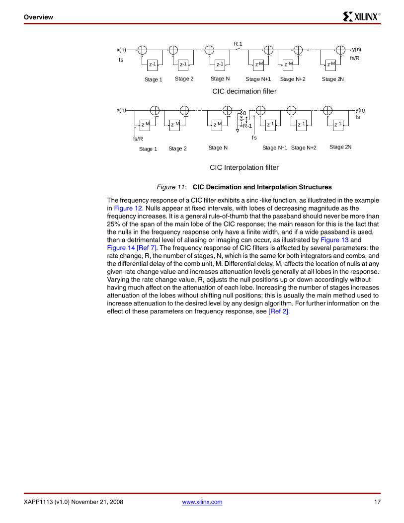
CIC filters use only delays and summation units and do not require multiplication operations as in an FIR filter. The filters are constructed from Integrator and Comb filter stages (Figure 10). A rate change is always involved in CIC filtering, and the filter response exhibits linear phase.
CIC filters can efficiently perform either decimation or interpolation, with two complementary structures being employed to implement these functions. Decimation requires a cascade of a number of integrator units, followed by a down-sampling stage and finally a cascade of the comb filter units. Conversely, interpolation cascades several comb filters with an up-sampler and several integrators. These cascades are illustrated in Figure 11.
X-Ref Target - Figure 10
Figure 10: CIC Component Stages
Integrator Comb Filter
Overview
XAPP1113 (v1.0) November 21, 2008 www.xilinx.com 17
R
The frequency response of a CIC filter exhibits a sinc -like function, as illustrated in the example in Figure 12. Nulls appear at fixed intervals, with lobes of decreasing magnitude as the frequency increases. It is a general rule-of-thumb that the passband should never be more than 25% of the span of the main lobe of the CIC response; the main reason for this is the fact that the nulls in the frequency response only have a finite width, and if a wide passband is used, then a detrimental level of aliasing or imaging can occur, as illustrated by Figure 13 and Figure 14 [Ref 7]. The frequency response of CIC filters is affected by several parameters: the rate change, R, the number of stages, N, which is the same for both integrators and combs, and the differential delay of the comb unit, M. Differential delay, M, affects the location of nulls at any given rate change value and increases attenuation levels generally at all lobes in the response. Varying the rate change value, R, adjusts the null positions up or down accordingly without having much affect on the attenuation of each lobe. Increasing the number of stages increases attenuation of the lobes without shifting null positions; this is usually the main method used to increase attenuation to the desired level by any design algorithm. For further information on the effect of these parameters on frequency response, see [Ref 2].
X-Ref Target - Figure 11
Figure 11: CIC Decimation and Interpolation Structures
y(n)
z-M
x(n)
z-1 z-1 z-1
R:1
z-M z-Mfs fs/R
Stage 1 Stage 2 Stage N Stage N+1 Stage N+2 Stage 2N
CIC decimation filter x(n) y(n)
fs
z-1 z-1 z-1
0
R-1fs
z-M z-M z-M
fs/R
Stage 1 Stage 2 Stage N Stage N+1 Stage N+2 Stage 2N
CIC Interpolation filter

Overview
XAPP1113 (v1.0) November 21, 2008 www.xilinx.com 18
R
X-Ref Target - Figure 12
Figure 12: Example CIC Magnitude Response Plot
X-Ref Target - Figure 13
Figure 13: CIC passband Aliasing

Overview
XAPP1113 (v1.0) November 21, 2008 www.xilinx.com 19
R
One important consideration in the use of CIC filters is the problem of “passband droop.” In almost all systems, a flat passband in the magnitude frequency response is desirable to prevent signal distortion. However, as described earlier, CIC filters exhibit a sinc-like frequency response, which can decay appreciably even within the passband when there are many stages or a high rate change. Therefore, it is necessary to cascade the CIC filter with an FIR filter which compensates for this droop with an inverse-sinc frequency response. Figure 15 illustrates this passband droop, the compensation response, and the composite response. Often the compensation filter (or CFIR) incorporates an interpolation step of two, which may reduce the number of stages (and therefore resources) required in the CIC filter.
Figure 16 shows the CIC Compiler token from the Xilinx blockset library in System Generator, with its GUI alongside. The block’s port configuration is described in Table 3. For more detailed information on the operation of the CIC Compiler block, see the block’s documentation in System Generator and the data sheet for the underlying CORE Generator IP core Figure 2.
X-Ref Target - Figure 14
Figure 14: CIC Passband Imaging
X-Ref Target - Figure 15
Figure 15: Illustration of Passband Droop Compensation

Overview
XAPP1113 (v1.0) November 21, 2008 www.xilinx.com 20
R
X-Ref Target - Figure 16
Figure 16: CIC Compiler Token and GUI in System Generator
Table 4: System Generator CIC Compiler Block Interface
Port Name Direction Description
din Input Input data samples. If multi-channel operation is selected, this is input in TDM fashion over N consecutive cycles, where N is the number of channels required.
nd Input New Data. Input data validation strobe.
dout Output Filtered output data samples. If multi-channel operation is selected, this is output in TDM fashion over N consecutive cycles, where N is the number of channels required. For interpolators, this usually means outputs are continuously valid, while for decimators, this means outputs are valid for N cycles followed by a long gap before the next group of samples for each channel.
din
nd
dout
rfd
rdy
chan_sync
chan_out
cic_i _int16x_1v1

Overview
XAPP1113 (v1.0) November 21, 2008 www.xilinx.com 21
R
Critical Design Parameters for DUC/DDC Systems
There are a number of design parameters that are critical to selecting the appropriate architecture for a DUC or DDC system.
Total Rate Change
The total rate change through the DUC/DDC system is almost certainly the most important parameter to be considered. Where the total rate change is low (e.g., less than 32), the interpolation or decimation stages may be achieved effectively with a cascade of FIR filters (see [Ref 1] for more information on this type of implementation); where the total rate change is high, FIR filters would not be the most efficient choice and CIC filters should be considered (in combination with FIR filters) as a more efficient alternative. This scenario is described in the examples in this application note.
Clock Rate
The clock rate of the circuit determines how many operations can be performed in a single sample period, which in turn affects how much hardware folding can be achieved by each function. This ratio alters as the signals proceed down the processing chain; at the highest sample rates, multiple modules may be required to process the data samples.
Number of Carriers (or Subcarriers)
The number of carriers to be supported has a significant bearing on architecture choices on several levels. At the system level, single carrier systems or those with small numbers of carriers (or subcarriers) are best suited to the architecture described in this Application Note; larger numbers of carriers or subcarriers may be better suited to channelizer architectures based on FFT techniques. At a module level, the number of carriers is related to the number of data channels implemented in each functional block, and a higher carrier count reduces the level of hardware folding achievable.
Number of Channels
Although it is often the case, the number of channels required is not necessarily directly related to the same as the number of carriers. For instance, in MRI systems, the center frequencies are the same for each channel; therefore, a single sinusoid can be used to mix with multiple channels of sample data.
Passband WidthThe passband width refers to the spread of possible frequencies to which the user may wish to up-convert the modulated data signals. For instance, this might refer to the entire GSM transmission band, or the spectral range of an MRI machine. In multi-carrier systems, this parameter determines the minimum sample rate that can be used for mixing channel data, as the sample rate must be sufficient to cover the frequency spread. The passband width also has a bearing on digital pre-distortion algorithm implementations, which usually operate at a sample rate which is at least an integer multiple (4x or 5x) above the passband width.
rfd Output Ready For Data. Handshaking signal for flow control with preceding stage. Data is not accepted by the block if this is deasserted.
rdy Output Ready. Output data validation strobe.
chan_out Output Indicates the channel with which the output data is associated
chan_sync Output Indicates the timing of the first channel of a multi-channel output sequence.
Table 4: System Generator CIC Compiler Block Interface (Cont’d)
Port Name Direction Description

Overview
XAPP1113 (v1.0) November 21, 2008 www.xilinx.com 22
R
One important implication of this parameter for this application note relates to the bulk rate change of the CIC filters which are used in the narrowband system examples. As stated above, mixing must occur at a sample rate which is greater than the passband width; however, with CIC filters, the input sample frequency may be too low while, due to the large rate change, the output sample rate may be higher than required and, therefore, utilizes more resources than are strictly necessary for the mixer implementation, due to a low number of clocks per sample period.
Modulation Scheme
The modulation scheme can have an effect upon the input rate of the DUC and the output rate of the DDC. Some modulators are over-sampled by nature of their implementation (see the GMSK example, later) and this reduces the overall rate change of the DUC. Some demodulation schemes require an over-sampled version of the data to provide effective demodulation of the symbol or to allow the possibility of timing recovery, which again reduces overall rate change.
Another issue with modulation schemes is the supported symbol rates. Where multiple symbol rates are to be supported, a greater degree of flexibility is required in the processing chain (to match up sample rates), and therefore the bulk rate changes of a CIC filter can be a disadvantage. FIR filters are more suitable for such complex DUC/DDC applications.
Supported Standards
For wireless communications systems where multiple air standards are to be supported in the same DUC/DDC system, the system needs greater flexibility to match up sample rates to a common rate for combination. Fractional resampling may provide a suitable solution for rate matching in such complex systems. This application note addresses only single air standard solutions.

Application Example: Multi-Carrier GSM (MC-GSM)
XAPP1113 (v1.0) November 21, 2008 www.xilinx.com 23
R
Application Example: Multi-Carrier GSM (MC-GSM)
Application Overview
Although Global System for Mobile (GSM) communication is now well into its second decade of operational use, it is still a highly significant market segment for base-station manufacturers. This is partly due to legacy and transitional installations in existing markets, but also due to significant opportunities in emerging markets, such as Africa and more remote regions of Asia and South and Central America where the base-station infrastructure is still being expanded.
In legacy GSM systems, multiple carrier capability has generally been provided by separate digital generation of each channel followed by analog combination for transmission. Such analog combiner circuits can be complex and expensive and can introduce significant noise and distortion. Digital combination would be preferable, but the performance requirements of the converters in such a system would have been too high. GSM is one of the more difficult air standards to meet, and multi-carrier operation for GSM requires even higher effective dynamic range, meaning converters require low Spurious-Free Dynamic Range (SFDR), Inter-Modulation Distortion (IMD), and high Signal-to-Noise Ratio (SNR). Performance of Analog-to-Digital Converters (ADCs) and Digital-to-Analog Converters (DACs) in the recent past was insufficient to meet these criteria and was the limiting factor in the signal processing chain. However, the latest generation of converters can now match or exceed the critical performance metrics [Ref 8] [Ref 9].
Recent work by the GSM-EDGE Radio Access Network (GERAN) group of the 3rd Generation Partnership Project (3GPP) has led to relaxation and clarification of some of the requirements of GSM networks in the presence of other carriers in the transmission path. This development, along with the advancements in converter technology mentioned above, has made co-location of multi-carrier capable, and indeed multi-standard capable, base-stations both feasible and commercially attractive. Multi-carrier GSM is therefore an area of interest for many base-station manufacturers.
Remote Radio Head (RRH) architectures are another driving force in the development of further digital integration. In these systems, the radio front end is housed at or near the top of the mast, with a high-speed digital serial connection to the main base-station equipment below. This is highly desirable, as the cabling from an RF unit at the base of the mast to the top could drop as much as 6 dB. Therefore, there is significant opportunity for OPEX savings, as well as the CAPEX savings generally achieved through greater digital integration.
A key enabler for multi-carrier systems in general has been the development and use of Crest Factor Reduction (CFR) algorithms. Gaussian Minimum Shift Keying (GMSK) modulation provides a constant envelope for a single carrier, which is good for Power Amplifier (PA) efficiency. However, combining multiple carriers modulated with GMSK increases the Peak-to-Average Power Ratio (PAPR) of the signal, which increases the required back-off of the PA and reduces efficiency. CFR methods (e.g., pulse cancellation, peak windowing) can significantly alleviate this problem. Xilinx offers a pulse cancellation CFR (PC-CFR) module (see [Ref 10]). It is worth noting that CFR algorithms often operate at multiples of the DAC frequency.
The development of Digital Pre-Distortion (DPD) techniques has further enabled efficiency improvements (or cost reduction for the same performance) in power amplifiers (PAs) by compensating for non-linearities. This also makes multi-carrier systems more feasible and economically viable. Xilinx also offers a DPD solution (see [Ref 11]), which can be tailored to various PAs.
The DUC/DDC pair in this example is designed to meet the 3GPP TS 45.005 specification [Ref 12], which defines the radio frequency transmission and reception requirements for GSM base-stations. Many designs have been in use for many years for single-carrier DUC/DDC circuits which meet this specification; these generally have employed CIC filtering as a basis. Using the powerful capabilities of Xilinx FPGAs to handle multiple channels simultaneously and a portfolio of class-leading DSP IP cores to exploit these capabilities, this example provides a guide to converting the common single-channel GSM DUC and DDC structures to efficiently implement multi-carrier functionality.

Application Example: Multi-Carrier GSM (MC-GSM)
XAPP1113 (v1.0) November 21, 2008 www.xilinx.com 24
R
Digital Up-Converter
Performance Requirements
A summary of requirements for the downlink transmit path is listed inTable 5. These requirements assume a normal base transceiver station (BTS) operating in the GSM 900 band.
Spectral Mask Requirements
The GSM spectral mask requirements for transmission, determined by Section 4.2.1(Spectrum due to the modulation and wideband noise) [Ref 12] and Section 4.7.2 (Intra BTS inter-modulation attenuation) [Ref 12], are summarized in Table 6. These requirements assume a normal BTS operating in the GSM 900 band.
Note: The adjusted attenuation figures have been modified using the specified method of adding
Table 5: Target Specification for GSM Downlink Transmit Path
Parameter Value Comments
Channel Bandwidth 200 kHz
Number of Carriers 4
Baseband Symbol Rate 270.8333 kbaud
IF Sample Rate 69.3333 Msps 256 × 270.8333 kbaud
Transmit Spectral Mask Up to 91.2 dB for frequency offset over 6 MHz
Sections 4.2.1 and 4.7.2 of [Ref 12] require 85.2 dB, plus 6 dB to allow for four carriers
Modulation Accuracy 5 degrees RMS phase error
Input Signal Quantization 12-bit I and Q Complex
Output Signal Quantization 16-bit I and Q Complex output is more general than real output
Mixer Properties Tunability: VariableResolution: ~0.25 HzSFDR: up to 115 dB
Table 6: GSM Spectral Mask Requirements for Transmission
Frequency Offset from Carrier (kHz)
Attenuation (dB)
Measurement Bandwidth (kHz)
Adjusted Attenuation (dB)
< 100 +0.5 30 +0.5
> 100 -30 30 -30
> 200 -33 30 -33
> 400 -60 30 -60
> 600 -70 30 -70
> 1200 -73 30 -73
> 1800 -75 100 -80.2
> 6000 -80 100 -85.2
⎟⎟⎠
⎞⎜⎜⎝
⎛×
1
210log10
BWBW

Application Example: Multi-Carrier GSM (MC-GSM)
XAPP1113 (v1.0) November 21, 2008 www.xilinx.com 25
R
to the specified value, where BW1 is the lowest measurement bandwidth and BW2 is the higher measurement bandwidth. The spectral mask defined above is shown in Figure 17, centered at baseband. Strict compliance is assumed; therefore, the intermediate mask values are interpolated from the given values.
DUC Input
The input to the DUC is provided by a modulator function. GSM systems use a number of different modulation schemes, which are described briefly in the following sections.
GMSK Modulation
GMSK is the technique used to modulate data for transmission in GSM systems. It is based on MSK, which has linear phase changes and is spectrally efficient. GMSK uses a Bandwidth-Time (BT) product parameter which controls how much the data symbols should overlap, and produces a spectrally efficient modulation at the expense of some inter-symbol interference (ISI). The symbol rate defined by the GSM specification is 1625/6 kbaud, or approximately 270.8333 kbaud. The BT product for GSM systems is specified as 0.3, which results in tightly controlled spectral width. Generally, GMSK modulators produce a version of the desired GMSK waveform which is over-sampled by a particular factor, typically 8.
Another significant advantage of GMSK modulation is its constant envelope modulation, which allows power amplifiers to operate at their most optimal biasing point and linearity is not a concern (linear power amplifiers are more expensive than non-linear amplifiers with equivalent power handling). This point is worth noting, because we are looking at a multi-carrier example. When multiple uncorrelated GMSK-modulated signals are combined, the resultant signal does not have a constant envelope, which removes this benefit (the implications of this for wider system design will be touched on later).
Current implementations of GMSK modulators take advantage of the fact that there is a limited set of frequency trajectories within the symbol structure, which may be stored in a look-up table and addressed by a vector created by the recent input data history [Ref 13] [Ref 14]. This is a highly efficient method when compared to previous implementations that employed filtering and integration methods, as it can be implemented very effectively in digital circuits.
X-Ref Target - Figure 17
Figure 17: GSM Transmission Spectral Mask

Application Example: Multi-Carrier GSM (MC-GSM)
XAPP1113 (v1.0) November 21, 2008 www.xilinx.com 26
R
GMSK modulation is used as the source of modulated data input to the DUC circuit described in this example. A Simulink® model of a multi-channel GMSK data source (gmsk_mod.mdl) is used to generate the sample data required (spectrum shown in Figure 22, along with the GSM transmit spectral mask), at an over-sampling rate of 8. The Simulink model of the modulator is run automatically by the model script, if required, to regenerate the input vectors.
A visual demonstration of the GMSK modulator model can be observed by opening and running the accompanying Simulink model, gmsk_mod_demo.mdl, in the model directory. The Scatter Plot (Figure 19) demonstrates the movement around the circular constellation with the desired Gaussian step profile, and the Eye Diagram (Figure 20) illustrates the limited set of phase transition vectors which are exploited by the modulator methods described in [Ref 13] and [Ref 14].
X-Ref Target - Figure 18
Figure 18: Spectrum of GMSK Modulated Signal
X-Ref Target - Figure 19
Figure 19: Scatter Plot of GMSK Modulated Data

Application Example: Multi-Carrier GSM (MC-GSM)
XAPP1113 (v1.0) November 21, 2008 www.xilinx.com 27
R
This example design does not include the modulator design; suitable circuits to implement this type of GMSK modulator can be readily inferred from the reference material. The assumptions for the example design are that the over-sampling rate for the modulator is 8, the sample outputs are complex, and the quantization of modulator output samples is 12-bits.
EDGE
Enhanced Data rates for GSM Evolution (EDGE) is an enhancement to the GSM specification that aims to provide higher data rates by using a higher order modulation scheme while maintaining a similar spectral profile to the original GMSK scheme (Figure 21, taken from [Ref 15]). EDGE uses a 3pi/8-QPSK modulation scheme, which provides 2 bits per symbol, thereby doubling the effective data rate with respect to GMSK modulation while emulating its spectral efficiency. The modulation scheme results in signal vector changes which avoid going through the constellation origin, and which minimize peak to average power ratio (PAPR). While EDGE functionality is not specifically covered by this Application Note, the fact that the spectral profile of modulated EDGE data is a close match for that of GMSK-modulated data makes the structures it describes generally applicable to EDGE systems (although possibly some small adjustment of filter requirements would be necessary).
X-Ref Target - Figure 20
Figure 20: Eye Diagram of GMSK Modulated Data, Illustrating Frequency Trajectories

Application Example: Multi-Carrier GSM (MC-GSM)
XAPP1113 (v1.0) November 21, 2008 www.xilinx.com 28
R
Evolved EDGE
Evolved EDGE (or e-EDGE, or EDGE2) uses a higher baseband symbol rate of 325 kbaud (1625/5 kbaud) along with higher order modulation schemes (up to QAM-64, with 6-bits per symbol) to provide users with significantly higher data rates than GSM or EDGE.
Evolved EDGE systems are generally required to accommodate traffic that complies with the GMSK and EDGE modulation schemes at the normal symbol rate on a slot-by-slot basis. As a result, the variable symbol rates require a more complex and flexible system with adaptable symbol rate changes within the filter chain; this will most probably require a multi-stage FIR implementation rather than a CIC-based design. This enhanced functionality is not covered by this example.
DUC Filter Design
The MATLAB function gsm_duc_cic_filters.m in the model subdirectory of the example is used to design the filters used in this example; refer to the script for details of the filter implementations described below.
Architectural Consideration
One of the assumptions for this example is the inclusion of a CIC filter, as DUC architecture involving FIR cascades has already been covered in [Ref 1].
The general structure for the example DUC filter design follows a pattern common in DUC implementations that utilize CIC filters. It involves a three-stage filtering process, as illustrated in Figure 22.
X-Ref Target - Figure 21
Figure 21: Spectral Comparison of GSM and EDGE
X-Ref Target - Figure 22
Figure 22: 3-Stage CIC-Based DUC Filtering
X
~
Modulator PFIR CFIR
CIC
Mixer
Sinusoidx1113_22_101508
M 2 2 N
Application Example: Multi-Carrier GSM (MC-GSM)
XAPP1113 (v1.0) November 21, 2008 www.xilinx.com 29
R
The modulator has some bearing on the filter chain, as there may be an over-sampled symbol output, which can affect the requirement for the overall up-sampling factor. The first filter performs pulse-shaping, for matching to a desired spectral profile or channel requirement, and also commonly provides an interpolation step in the up-conversion process (usually by 2). The second filter provides compensation for the passband droop introduced by the CIC filter, described earlier, by pre-emphasizing the passband data with an appropriate inverse frequency function. It also commonly provides a further interpolation stage, up-sampling by a factor of 2 normally. The CIC function is the final stage in the filter chain, and provides the bulk of the total DUC rate change. The CIC output is then mixed with the sinusoid before passing to the output of the DUC.
This structure can be readily adapted to a multi-carrier configuration by using multiple channels for the filter sections and a vector dot product operation for the mixer; these adaptations are well-suited to the latest Xilinx® FPGAs (using SRL16 elements for multi-channel support in filters and DSP48 slices for the mixer). Therefore, this structure is used as the basis of this example.
Common Parameters and Assumptions
The input and output rates of the filter chain are important parameters in the general filter design process. A common value for over-sampling of the symbol rate seen in GMSK modulator implementations is 8, which is adopted in this application example. Therefore, the input rate to the filter chain is 8 times the symbol rate, or 2.16667 Msps. The output rate of the filter chain is the mixer output rate, which is at the intended DAC sample conversion rate or a small integer factor thereof. The selected rate is 256 times the symbol rate, or 69.3333 Msps, which is within the capabilities of low-cost components. The overall rate change for the DUC filter chain from modulator output to mixer input is, therefore, 256/8 = 32.
The passband for filter design is set to 80 kHz, which is the normal GSM band of interest; it should be noted that in EDGE or Evolved EDGE systems, this might need to be wider to allow for different modulation schemes. The stopband edge is set at 100 kHz, due to the spectral mask requirements defined by the 3GPP specification at that frequency.
The passband ripple used for specification of each filter in the cascade is set an order of magnitude less than the absolute specification for the DUC to minimize the overall ripple when the filter cascade is combined. The stopband attenuation should be specified such that the minimum requirements of the GSM spectral mask are met. In general, this means attenuation of at least 86 dB, plus margin for later analog processing, although spectral shaping can be employed.
Pulse-Shaping Filter
In narrowband systems with higher order modulation schemes, such as QPSK or QAM, a pulse-shaping filter would generally be required in the DUC to filter and shape the symbol waveforms produced by the modulator. However, as described earlier, an efficiently designed GMSK modulator produces a suitably shaped spectral profile, therefore, pulse-shaping filtering is often not required for GMSK modulated data. The example filter design script does include the capability to generate a Pulse-Shaping Filter (PFIR) design, but this is disabled for the example – users may experiment with the PFIR both included in and excluded from the filter cascade if they wish.
If the EDGE data modulation scheme were to be used instead (or alongside) of GMSK, the PFIR could be used as the pulse-shaping filter to limit any spectral content introduced by the constellation mapping quantization. Note that the there is scope with the filter implemented (but bypassed) in the example design to increase the passband edge slightly from 80 kHz, without incurring a significant additional hardware cost, as the passband to stopband edge is still quite sharp even with the limited tap count. Provided that the 100 kHz stopband edge is maintained, the 80 kHz value may be increased slightly if required.

Application Example: Multi-Carrier GSM (MC-GSM)
XAPP1113 (v1.0) November 21, 2008 www.xilinx.com 30
R
If Evolved EDGE data modulation schemes (up to 64-QAM) were to be used, the PFIR would become a much more important and complex component of the filter chain, as these modulation schemes often result in spectral profiles which extend beyond the normal GSM band of interest. Such cases are not specifically addressed in this example, although similar filter specification and generation techniques may be employed to achieve this.
CIC Filter
The CIC filter is arguably the most important filter in the chain, as it achieves the bulk of the rate change in the system, and its characteristics directly affect the frequency response requirements of the CFIR.
The required DUC rate change is 32, with no PFIR, and a rate change of 2 in the CFIR. Therefore, the rate change of the CIC is set to 16 (this is probably close to the minimum rate change for which one would consider a CIC filter over a FIR alternative).
The next most significant parameter of a CIC filter is the stopband attenuation, often specified as the required attenuation at the leading edge of the reflection of the passband with respect to the first null frequency. Increasing this attenuation value may be achieved by varying a number of design parameters, as was described in the introductory section. Increasing the differential delay of the comb sections can be an effective means of increasing stopband attenuation, but results in greater passband droop, which, even when compensated for, can distort passband data. Increasing the number of stages is the other major parameter change, and it is used here to achieve the desired attenuation. MATLAB is used to determine how many stages are needed in the CIC by specifying the fixed rate, the fixed differential delay, and the desired attenuation value of 96 db (86 dB + 10 dB margin)––the filter design script provides an example filter call based on these parameters. The result is a 4-stage CIC filter, with the frequency response shown in Figure 23.
Note: Since CIC filters use integer operations, there is no coefficient quantization; therefore, the reference and quantized filters are identical.X-Ref Target - Figure 23
Figure 23: Magnitude Response of CIC Filter

Application Example: Multi-Carrier GSM (MC-GSM)
XAPP1113 (v1.0) November 21, 2008 www.xilinx.com 31
R
CIC Compensation Filter (CFIR)
The CIC compensation filter (CFIR) is an interpolating low-pass FIR filter. It provides a further increase in sample rate, reducing the requirements on the CIC and limiting the number of stages required, while also providing moderate passband filtering of the GMSK modulated signal (although this requirement is less stringent where an effective GMSK modulator with good pulse-shaping properties has been used). An important additional function provided by the CFIR is compensation for the passband droop introduced by the CIC filter.
To specify the CFIR filter, the example MATLAB filter design script uses an equiripple technique (firceqrip). This function allows the passband to be modified with an inverse-sinc function to compensate for the passband droop of the CIC filter, with the power of the inverse-sinc function being matched to the number of stages in the CIC. The function is also useful for matching to spectral masks, as the stopband attenuation can be specified with a slope––this is a less important feature in this example. See the example script for details of the function call and parameter specification. The script also has an optional alternative technique using MATLAB’s built-in CIC compensation filter method, but which is not used directly in the example and only provided for the reader’s information. Many other filter design techniques are available in MATLAB. Refer to the product documentation for detailed information on their advantages and disadvantages.
To minimize the resources required for implementing the filter, the filter order can be limited such that it can be implemented in a single MAC unit (at a cost of one DSP48 slice), then the response is examined to see if it meets our requirements. If the requirements cannot be achieved in a single MAC, the filter order achievable in two MACs (at a cost of three DSP48 slices) can be calculated; no more than two MACs should be required given the requirements and sample rates, but the loop can be expanded as necessary. The filter order that is achievable in a single MAC unit is 30 (31 filter taps).
The attenuation in the stopband is set to an initial value at the stopband edge of 90 dB, with a slope of 80 dB per radian per sample thereafter (although the slope parameter in this example is used simply as a means of stopband ripple control). The script has loops built-in to allow architectural exploration. However, the filter choice from the loop results is currently hard-coded. The loops are retained in the example code to illustrate how such architectural exploration can be easily achieved, and the reader is free to experiment with other options for CFIR generation. The filter response achieved by this function is shown in Figure 24. Filter coefficient quantization has been selected to suit the DSP48 slice’s capabilities, so a quantization to 18-bits has been used. The quantized response is also shown in the Figure 24.X-Ref Target - Figure 24
Figure 24: Magnitude Response of CFIR Filter

Application Example: Multi-Carrier GSM (MC-GSM)
XAPP1113 (v1.0) November 21, 2008 www.xilinx.com 32
R
The combined frequency response of the CIC and its compensation filter should balance out the droop in the passband. This can be seen in Figure 25, although it also shows the limited extent of the passband droop in this case, due to the relatively small rate change value and the low number of stages required.
Composite Filter Response
The frequency-magnitude response of the combined filter cascade is shown in Figure 26. Both reference and quantized responses are provided.
The main point to note from this response is that the most significant artifact in the stopband is due to the remnants of the first and second lobe around the first null, where the passband of the CFIR has an interpolation image. This is the performance requirement that the MATLAB CIC filter function’s attenuation parameter (described earlier) attempts to address. The interaction of the various filters can be better observed in an overlay of the frequency responses, as shown in Figure 27.
X-Ref Target - Figure 25
Figure 25: Passband Zoom Overlay of CIC, CFIR, and Combined Frequency Responses
X-Ref Target - Figure 26
Figure 26: Overall DUC Filter Response

Application Example: Multi-Carrier GSM (MC-GSM)
XAPP1113 (v1.0) November 21, 2008 www.xilinx.com 33
R
Frequency Translation
After filtering and up-converting the baseband signal, the signal spectrum of each channel is shifted from baseband to a set of intermediate frequencies in the range of [-Fs/2, Fs/2], where Fs = 69.3333 MHz. A common separation for such multi-carrier GSM systems is 600 kHz (three channel widths). The DDS generates a vector of local oscillators to mix with the channel data, shifting the spectra of each channel up or down by the appropriate amount and creating a new multi-carrier baseband.
Due to the requirement in a multi-carrier GSM system for high dynamic range, the spectral purity and SFDR of the DDS are critical. Therefore, the highest performance options have been selected for the DDS Compiler. Taylor series correction phase dithering is employed to maximize overall performance of the DUC system while still achieving an acceptable resource cost for the implementation.
Table 7 lists a summary of parameters for the DDS block for the multi-carrier GSM.
The output frequencies and phase offset can be defined as constants or can be set dynamically through optional input ports. In this design example, the output frequency is programmable and the phase offset is set to zero. Both Sine and Cosine output are required for complex mixing. For programming, the desired output frequency value is defined in terms of normalized frequency, in units of cycles per sample. To generate an output frequency at fc MHz from the DDS at a sample rate of fs, the data port must be programmed with a value of fc/fs. The value should be quantized (using rounding) to the width of the DDS phase accumulator––in the
X-Ref Target - Figure 27
Figure 27: Overlay of DUC Filter Responses
Table 7: Summary of Key Parameters to Program DDS Compiler for MC-GSM
Parameter MC-GSM DUC Example Setting
DDS Clock Rate 69.333 MHz
Output Function Both Sine and Cosine
Spurious free dynamic range 115 dB
Frequency Resolution 0.25 Hz
Number of Channels 4
Output Frequency Programmable
Noise Shaping Taylor Series Corrected

Application Example: Multi-Carrier GSM (MC-GSM)
XAPP1113 (v1.0) November 21, 2008 www.xilinx.com 34
R
example, due to the high SFDR requirement for MC-GSM, the phase accumulator width is 32 bits.
The output width of the DDS sine and cosine samples is increased due to the Taylor Series correction, which adds additional LSBs on top of the look-up table output from RAM (which is 18-bits to suit the Xilinx block RAM size). In the example case, the DDS output sample width is 21-bits. This has implications for mixer implementation, as the wider input of the Virtex®-5 FPGA multiplier must be used for the DDS sample, leaving only the 18-bit input for the data samples. This is sufficient for the example in this application note, but readers may wish to consider a lower DDS sample width and wider data sample width at the mixer input.
DUC Modeling and Performance
A behavioral model of the DUC was created in MATLAB, with quantization and alignment options for matching to the hardware implementation. The MATLAB script gsm_duc_cic_model.m can be found in the subdirectory of the example. See this model for further detail on the modeling and performance described in Table 8.
The parameters relevant to the overall design are shown in Table 8. These are grouped at the top of the script to allow for easy modification and experimentation by the interested reader. Several other parameters are calculated from these variable parameters.
The GMSK modulated input to the DUC is shown in Figure 28. This is filtered by the CFIR defined in Section 2.2.3.5 [Ref 12], and the output power spectral density is shown in Figure 28, along with the GSM transmit mask; as can be seen, the spectrum meets the mask requirements (note that the tails on the spectrum are due to sample length rather than any systematic limitation in performance).
Table 8: Model Parameters
Parameter Description Example Default Notes
n_carr Number of carriers 4
m_duc Total rate change of DUC 256
fsym Symbol rate 1.625e6/6 Kbaud
clk_os Clock Over-sampling 4 Ratio of clock rate to sample rate; determines hardware resource sharing that can be achieved.
m_gmsk Over-sampling of GMSK modulated data
8 Typical value for digital implementation of GMSK.
m_pfir Rate change of PFIR 1 PFIR not used
m_cfir Rate change of CFIR 2
carriers Vector of carrier frequencies -0.9; -0.3;+0.3; +0.9
600 kHz carrier separation is common.
scale_vector Vector of scaling factors 1.0 (all) Optional scaling factor for each channel.
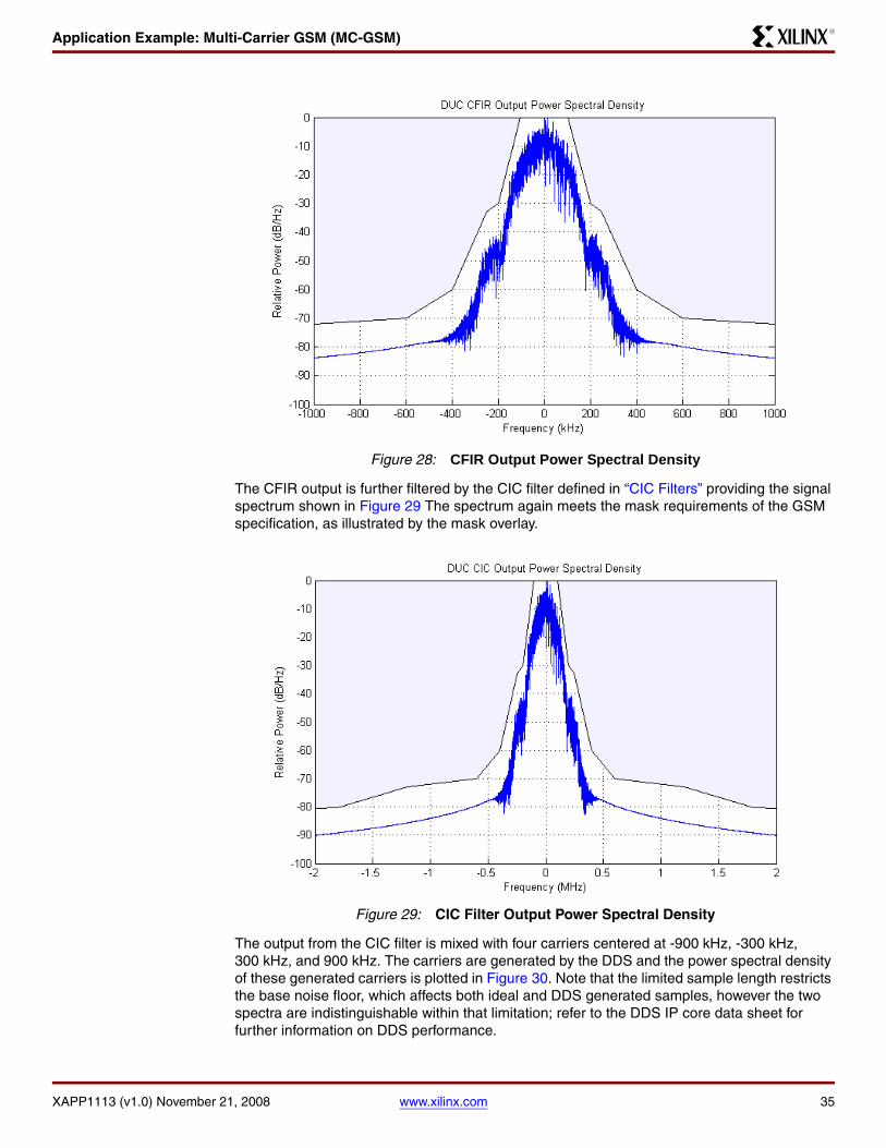
Application Example: Multi-Carrier GSM (MC-GSM)
XAPP1113 (v1.0) November 21, 2008 www.xilinx.com 35
R
The CFIR output is further filtered by the CIC filter defined in “CIC Filters” providing the signal spectrum shown in Figure 29 The spectrum again meets the mask requirements of the GSM specification, as illustrated by the mask overlay.
The output from the CIC filter is mixed with four carriers centered at -900 kHz, -300 kHz, 300 kHz, and 900 kHz. The carriers are generated by the DDS and the power spectral density of these generated carriers is plotted in Figure 30. Note that the limited sample length restricts the base noise floor, which affects both ideal and DDS generated samples, however the two spectra are indistinguishable within that limitation; refer to the DDS IP core data sheet for further information on DDS performance.
X-Ref Target - Figure 28
Figure 28: CFIR Output Power Spectral Density
X-Ref Target - Figure 29
Figure 29: CIC Filter Output Power Spectral Density

Application Example: Multi-Carrier GSM (MC-GSM)
XAPP1113 (v1.0) November 21, 2008 www.xilinx.com 36
R
The PSD of one of the up-mixed channels (shifted to -900 kHz) is plotted in Figure 31. Note the compliance with the GSM mask once more.
Figure 32 shows the power spectral density for the combined 4 carrier GSM waveform, with the mask for each carrier overlaid.
X-Ref Target - Figure 30
Figure 30: PSD of DDS Generated Carriers vs. Ideal Sinusoidal Carriers
X-Ref Target - Figure 31
Figure 31: Single Carrier Mixed with -900 kHz Carrier

Application Example: Multi-Carrier GSM (MC-GSM)
XAPP1113 (v1.0) November 21, 2008 www.xilinx.com 37
R
The phase error requirement for the GMSK modulated signals is 5%. Taking the modulator input and applying up-sampling and mixing with ideal filters allows a comparison to be made with the DUC model performance. This shows that the phase error introduced by the DUC implementation is negligible (less than 0.1%) allowing significant leeway for further digital and analog processing.
DUC Implementation
The top-level block diagram for the multi-carrier GSM DUC implementation is shown in Figure 33. See the Simulink model for a more detailed view.
Initialization
An initialization process must be performed prior to running the System Generator model simulation. The script gsm_duc_cic_init.m must by run before using the System Generator model, as this establishes the correct environment and configuration for the System Generator
X-Ref Target - Figure 32
Figure 32: Power Spectral Density for Multi-Carrier GSM Waveform
X-Ref Target - Figure 33
Figure 33: Top-Level Block Diagram for MC-GSM DUC Implementation
In
wr_c h1
In
wr _ch
In
we1
In
we
In
wd at a1 In
wda ta
m c_m ix ed _vo ut
tw7
m c_m ix ed _q
tw6
cfir _d ou t
tw5
cic _i_ scal ed _d ou t
tw2
ci c_q _sca le d_ do ut
t w13
m c_ mi xed _i
tw1
wr _ch
wda ta
we
scal er_ p rog am
din
ch_in
vin
wr_ ch
wdat a
we
dout
ch _out
v out
sca ler In
q_ c7
In
q_ c6
In
q_ c5
In
q_ c4
din_i
din_q
vin
chin
wr _ch
wr _data
we
mixed_i
m ixed_q
v out
m ixe r
Out m ixe d_ vou t
Out m ixe d_ q
Out m ixe d _i
In
i _c7
In
i _c6
In
i _c5
In
i _c4
wr_ch
wdata
we
fr eq _p ro ga m
Out d at a_ loa d 1
din
vin
do ut
c ha n_ in
ch an _o ut
vo ut
31 Tap
I nte rp ol ate b y 2
cfi r_ int 2x_ 3v 1
r eset
ch 0
ch 1
ch 2
ch 3
ch 4
ch 5
ch 6
ch 7
q
ch _out
load
T DM 1
T 2
T1
T
n ot
Inv ert er 1
z- 9
De lay1
cast
Co nve rt
0
Con st an t1
din
v in
cha n_in
do ut_i
dout _q
vo ut
CI C_i pb uff
din_i
din_q
v in
dou t_i
dout _q
vou t
chou t
CI C
c1 _i
c1_q
c2 _i
c2_q
c3 _i
c3_q
c4 _i
c4_q
4 -ch GM SK1
Sy stemGenera tor
mc _mixed_im c_m ix ed_i
mc _mixed_ q
wr_ch
wdata
we
mc _mixed_ vout
cf ir_c han_out
cf ir_chan_ in
cfir _dout
cf ir_v out
c0_ i
tdm _ch_ou t
tdm _load
c2_ q
c2_ i
c1_ q
c1_ i
c0_ q
tdm _out
cf ir_v in
c3_ q
c3_ i
sca le r_dout
scaler _vout

Application Example: Multi-Carrier GSM (MC-GSM)
XAPP1113 (v1.0) November 21, 2008 www.xilinx.com 38
R
model to operate. The main function of this initialization script is to run the behavioral MATLAB model to setup parameter values and generate the filter designs. The MATLAB model also generates and saves sample data (in the results subdirectory) for comparison with the System Generator implementation as part of the verification process for the design.
Hardware Over-Sampling
The hardware over-sampling for the implementation is an important factor throughout the design and is usually determined by the ratio of the maximum achievable clock rate to the required output sample rate (and integer multiples thereof). For this example, the value could potentially be as high as 5, given the intended DAC conversion rate of 69.3333 Msps. However, there is a limitation with the current CIC Compiler System Generator block implementation that restricts hardware over-sampling to values such that the clock rate divided by the channel count is an integer multiple of the conversion rate. This reduces the potential over-sampling to a factor of 4, which is still a reasonable value for achieving an efficient implementation and would reduce the power utilization of the core.
Data Path Bitwidth
To achieve the high dynamic range required in MC-GSM systems, a bitwidth of 17 to 18 bits has been selected. This provides a theoretical dynamic range sufficiently higher than the desired 91.2 dB, leaving a little margin for other factors such as PA back-off, PAR variance, and so on, while still remaining within the capabilities of most DSP slice elements from current FPGA device families. 17-bits will be used for data input to symmetrical FIR filters, due to the requirement for a pre-adder before the multiplication stage in efficient FIR implementations.
GMSK Modulator
The GMSK modulation simulation model is the source on the right, followed by Gateway In blocks to quantize appropriately the input values to the System Generator design. As described earlier, this is a model for simulation only and is not included in the System Generator implementation of the DUC. See [Ref 13] and [Ref 14] for guidance on efficient digital implementation of GMSK modulators.
GMSK input data is quantized with 12-bit data sample width.
TDM
A time division multiplexer (TDM) is used to serialize the channel data for input into the CFIR filter (serial multi-channel filter implementation can be efficiently implemented in Xilinx® FPGA devices due to the SRL16 shift register element). The TDM module includes reset capability, for sample alignment, but that feature is not used in this example. Readers may wish to utilize this capability in their own designs for application specific purposes.
CFIR Filter
The implementation of the CFIR filter is a standard FIR Compiler System Generator component, using parameters (including the coefficient vector) based on MATLAB variables created by the model. Filter inputs and outputs are TDM in nature. The parameters for the core are generally defined by referencing MATLAB variables created by the model.
The coefficients of the CFIR filter are quantized by the MATLAB script already to 18-bits, with 17-bit input data width.
Programmable Channel Scaler
The CFIR output passes to a programmable scaler module that allows each channel to be scaled by a different scaling factor. With the low sample rate at this point, significant resource sharing can be exploited. Therefore, a single DSP48 slice coupled with a small Distributed RAM memory are main constituents of this circuit. Interested users can adjust scale factors by opening the block mask dialog box and entering new values, bearing in mind that the scaling of

Application Example: Multi-Carrier GSM (MC-GSM)
XAPP1113 (v1.0) November 21, 2008 www.xilinx.com 39
R
the data path is designed to handle four channels at a scaling of 1.0. Quantization ranges therefore may need adjustment should any significant increases above 1.0 be entered.
Another option for using the scaler module is for implementation of the GSM power-time mask. All channels may be switched on or off simultaneously for the requirement periods to implement the mask.
Interpolating CIC Filter
The CIC filter cannot directly use evenly spaced TDM data sample streams, as produced by other cores such as the FIR Compiler. Thus, an adaptation module is required to convert the output from the scaler to a format where the TDM data for the various channels is grouped into consecutive clock cycles for input into the CIC filter. Two Distributed RAM storage elements and a small logic circuit are required to perform this function. See the CIC Compiler data sheet [Ref 2] for further information on input timing for multi-channel interpolation filters and to the System Generator model for details on the adaptation module.
The CIC filters are implemented as two modules, with one filter handling In-Phase data for the four carriers and the other handling the Quadrature data. The parameters are generally entered manually, therefore, any user modification to the model must be matched manually.
Mixer
Figure 34 shows the System Generator design of the mixer block. See the System Generator model for a more detailed view.
To align the DDS output and the CIC output, some data muxing and scheduling are necessary. See the ch_align block within the mixer design. This interface module uses two Distributed RAM blocks to store data samples output from the CIC, which are then read from the RAM only when the DDS sample output for the corresponding channel is passed to the mixer multiplication unit.
The DDS is programmable, with the user having the capability to alter the carrier frequency values by changing the frequency values in the programming block at the top level of the design.
The multiplication unit employs a complex multiplier and accumulator, constructed from DSP48 slices. This unit makes use of the dedicated cascade routing and built-in data path delay units
X-Ref Target - Figure 34
Figure 34: Virtex-5 Mixer FPGA Implementation in System Generator Software
3
vo ut
2
m ixe d _q
1
m i xed _ i
In Ou t1
x2 ze ro
dd s_sg
tw
o u t
t_ flo p
0
ro un d60
ro un d50
ro un d4
0
ro un d30
ro un d20
ro un d1
se l
d 0
d 1
d 2
d 3
z-1
op m o de _m u x
z-2
o p _d ly_ m a tch 1
cha n ne lse l
da ta
we
sin
c os
ch a nn e l
m cg sm _ d ds
r ei nte rp re t
i nt eg er ize _ si n
r ei nte rp re t
in te ge ri ze_ co s
rei nt er pr et
in t_ q
re in te rpr et
in t_ i
z- 4
d sp_ d ly_ m at ch
↓4z-1
ds3
↓4z -1
d s2↓4z -1
d s1
re int er pr et
d ei nt _q
re in te rpr et
d e int _i
dina_i
dina_q
ch_ina
ch_inb
vin
doutb _i
v out
do utb_ q
ch _a lig n _i
c ast
ca st _sin
cast
ca st _q
ca st
ca st _i
c ast
c ast_ co s
d
e nqz-1
ca p tu re _q
d
e nqz-1
ca ptu re _ i
ab
a =bz-8
c ap tu re _e n
0
c1 T 5
T 4
T 3
T 2
T 1
P =PCI N+( A*B)
O pm o de 4
P=( A*B)
O pm o de 3
P= PCIN+ (A*B)
Op m od e 2
P= -(A*B)
Op m od e 1
P= PCIN+ (P)
Op 23 4
P= PCIN+ (C)
O p1
[ca p t_e n ]
G ot o
[c ap t_ en ]
Fr om
a
b
c
p cin
o p
p
DSP4 8_ Q 3
a
b
pci n
op
p
pco u t
DSP48 _ Q2
a
b
op
p
p cou t
DSP4 8_ Q 1
a
b
c
pc in
op
p
DSP4 8_ I3
a
b
pci n
op
p
pco u t
DSP48 _ I2
a
b
op
p
p cou t
DSP4 8_ I1
7
we
6
wr_ d ata
5
wr _ch
4
c hi n
3
vin
2
d in _q
1di n_ i
we dds_c hanne l
wr _dat a
wr _ch
dds_c os
d ds_sin
m ixed_i
m ix ed_q
din_i_aligned
a lig n_v outchin_i
din_i
din_q
din_q_align ed
i_int
opm ode
q _int
vin _i

Application Example: Multi-Carrier GSM (MC-GSM)
XAPP1113 (v1.0) November 21, 2008 www.xilinx.com 40
R
of these DSP slices to reduce routing congestion, increase maximum speed, and reduce power consumption. The multiplication unit is based on the complex multiplier illustrated in Figure 35.
The accumulator further expands on this design by using the same dedicated PCOUT-to-PCIN cascade paths to pass the mixed data for accumulation to two further DSP48 slices (one for I, one for Q). Rounding is also possible in this structure with minimal additional hardware requirements, using constant inputs to the multipliers’ C ports and appropriate OPMODE selection. These constant values and OPMODE switching circuits are shown in the mixer model.
Synthesis
The entire DUC design can be synthesized to produce an HDL netlist, NGC netlist, or bitstream using the Output options under the System Generator token GUI interface. Synthesis is performed by the user’s preference of synthesis tool, either XST or Synplify. NGC netlists are produced by XST only (this is a Xilinx-specific netlist in binary format incorporating constraints).
System Generator also produces a project file for the Project Navigator tool from the Xilinx ISE tool suite, which eases integration into larger designs. Using this project file, users can proceed to perform map and place and route tasks to further implement the design, or integrate with other circuits within the FPGA device. The ISE project file is created in the netlist directory specified in the System Generator token GUI, along with the design and its associated timing constraint file (XCF).
X-Ref Target - Figure 35
Figure 35: Complex Mixer Implementation with Cascaded DSP48 Slices
SU
B
C C
PCO
UT
CIN
CIN
SUB
BCIN
BCOUT
D D
D:A:B
SU
BSU
B
PC
IN
AA0 A1
PPB1
B B0 M
B1
A1
CC
PC
IN
SUB
CIN
CIN
SUB
BCIN
BCOUT
D D
D:A:B
SUB
SUB
PCO
UT
A A0
PPB B0 M
C C
PCO
UT
CIN
CIN
SUB
BCIN
BCOUT
D D
D:A:B
SUB
SUB
PC
IN
A A0 A1
PP
SUB
B1
B B0 M
B1
A1
CC
PC
IN
SU
BC
INC
INS
UB
BCIN
BCOUT
D D
D:A:B
SUB
SUB
PC
OU
T
A A0
PPB B0 M
Pr
Ai
Br
Bi
Pi
Ar

Application Example: Multi-Carrier GSM (MC-GSM)
XAPP1113 (v1.0) November 21, 2008 www.xilinx.com 41
R
DUC Verification
There are several methodologies which may be applied to the verification of a design implementation such as the DUC. The common aim of each should be to ensure as far as possible that the implementation meets the system-level requirements. One option to achieve this would be to simulate the System Generator implementation for long periods and perform detailed analysis of abstracted system-level performance. However, this approach can be time-consuming, especially when verifying a synthesized netlist, and slow to iterate when the system-level design changes. An alternative is to generate a sample-accurate and bit-accurate behavioral model of the design and compare the output of the model with the output of the implementation (both simulation model and synthesized netlist). The generation of the bit-accurate model can be time-consuming, but shorter simulations can provide a high level of confidence in the design implementation when directly matching the output signals sample-by-sample, bit-by-bit, at a number of key stages in the data path. Also, the turnaround time for design changes can be significantly faster.
Verification of the DUC System Generator implementation is performed by comparison of sample outputs at various stages in the design with those produced by the behavioral MATLAB model. The System Generator model includes several “To Workspace” sink blocks to direct output data samples to a MATLAB variable array for further analysis. The analyze_duc.m script may be run after the System Generator simulation, and this will compare the System Generator output values with those produced by MATLAB model. The script pauses and reports an error where a mismatch occurs. Figure 36 through Figure 38 provide examples of some of the output sample traces produced by the script, demonstrating the bit-accurate matching of the data samples.X-Ref Target - Figure 36
Figure 36: Comparative Analysis of CFIR Output Results – Exact Match

Application Example: Multi-Carrier GSM (MC-GSM)
XAPP1113 (v1.0) November 21, 2008 www.xilinx.com 42
R
One important point to note is that, due to a lack of a bit-accurate model of the DDS, the sinusoid generation function in the bit-accurate MATLAB model is performed by recording the sample output stream from a System Generator implementation of the DDS and using the vector created by this process as the sinusoidal carrier in the model. While this allows for a potential mismatch of functionality, the DDS core is a well-established core which has seen extensive verification and validation effort to compare its performance to ideal sinusoids (see the DDS Compiler data sheet [Ref 3] for further information).
The model-based verification method described here can allow rapid confirmation of the veracity of the System Generator implementation, matching the IP core block functions with standard MATLAB functions to provide a high level of confidence.
X-Ref Target - Figure 37
Figure 37: Comparative Analysis of Up-Mixed Multi-Carrier Signal – Exact Match
X-Ref Target - Figure 38
Figure 38: Zoom of Up-Mixed Multi-Carrier Signal Comparison

Application Example: Multi-Carrier GSM (MC-GSM)
XAPP1113 (v1.0) November 21, 2008 www.xilinx.com 43
R
DUC Resource Utilization
The DUC design was synthesized and targeted to a Virtex-5 device, XC5VSX50T, -1 speed grade, in an FF665 package. The estimated resource utilization of the DUC is summarized in Table 9.
The implementation of the CIC filters in the design does not use DSP slices by default, but an option is provided to users to prefer DSP slice utilization. With this configuration, the resource utilization is summarized in Table 10.
Note: Around 400 LUT-FF pairs are saved by this option, roughly equivalent to 100 slices depending on packing and configuration, while an extra 10 DSP slices are required; this trade-off is marginal at best in terms of both area (where one DSP slice corresponds to approximately 22 slices) and power (where the DSP slice consumes approximately the same as 14 slices, depending on configuration).
DUC Power Consumption
The estimated power consumption of the Virtex-5 FPGA DUC design, using the XPower Analyzer tool, is summarized in Table 11 and Table 12.
Note: The option of using DSP48 slices to implement the CIC filters results in marginally better power consumption, but it is not sufficient on its own to justify this choice. The resource usage must also be beneficial to the user, which may depend on other circuits implemented in the same device.
Table 9: Resource Utilization of 4-Carrier GSM DUC
Resource Type Number Required
DSP48Es 10
Block RAM 1
LUT-FF pairs 1935
LUTs 1225
FFs 1785
Table 10: Resource Utilization of 4-Carrier GSM DUC Using DSP Slices for CIC
Resource Type Number Required
DSP48Es 20
Block RAM 1
LUT-FF pairs 1540
LUTs 1105
FFs 1401
Table 11: Power Consumption of 4-Carrier GSM DUC Using Logic Slices for CIC
Power Type Power Value (W)
Quiescent (static) power 0.588
Dynamic power 0.178
Total power 0.766
Table 12: Power Consumption of 4-Carrier GSM DUC Using DSP Slices for CIC
Power Type Power Value (W)
Quiescent (static) power 0.587
Dynamic power 0.171
Total power 0.758

Application Example: Multi-Carrier GSM (MC-GSM)
XAPP1113 (v1.0) November 21, 2008 www.xilinx.com 44
R
Limitations of CIC-based DUC Implementation
One of the significant advantages of CIC filters is the efficient implementation of large rate changes, which has frequently been exploited in narrowband systems to good effect (since these systems by their very nature require large rate changes). For single carrier systems, this is a very efficient implementation technique, hence, the development of ASSP devices implementing the PFIR-CFIR-CIC structure for DUCs (for example, the GC4016 from Texas Instruments).
With multi-carrier systems, one of the most significant parameters in the architectural consideration is the mixer sample rate. This is because, as explained in “Mixers,” mixing for multi-carrier systems requires a dot product vector operation, which can involve many more operations than the simple multiplication step for a single-carrier implementation. Taking advantage of hardware resource sharing for these operations over multiple cycles can provide significant resource savings, but this requires multiple clock cycles per sample period. The more clocks per sample (in other words, the lower the sample rate), the fewer resources required; this is generally applicable to most digital hardware implementation of signal processing.
Unfortunately, the very advantage which has made CIC filters such a popular choice for narrowband systems becomes a disadvantage in multi-carrier implementation. The input rate to a CIC may be too low to allow multi-carrier mixing across a wide enough bandwidth, while the output rate may be too high to allow efficient resource sharing. Therefore, it is possible that DSP48 slices and other resources for implementing the mixer function might be reduced in a FIR-based solution. However, the extra resources required to implement FIR filters at ever increasing sample rates would more than balance out this saving.
Similarly, the large block rate change can become a disadvantage in systems where more flexibility is required, such as multi-standard BTS implementation. For support of multiple air standards, multiple data paths must at some point be merged, and finding a suitable common sample rate, or at least one which can be reached with a reasonable rational interpolation filter, is more difficult with the bulk rate change of the CIC. FIR-based solutions may have an advantage for such applications.
As has been mentioned previously, Evolved EDGE systems utilize a higher symbol rate than GMSK systems, which requires some flexibility in rate switching. This may be possible with CIC-based DUC implementation, but it is easier in FIR-based solutions, where a more flexible rate structure is used.
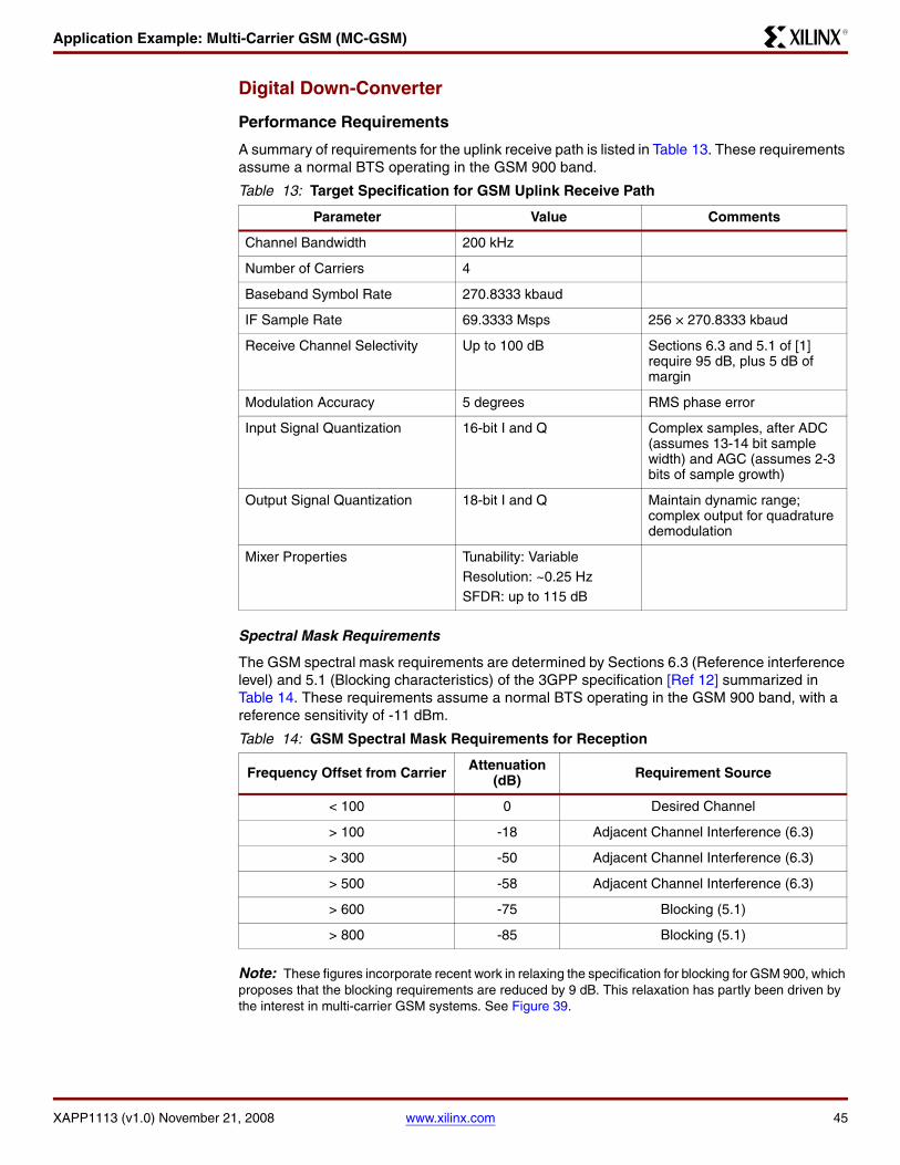
Application Example: Multi-Carrier GSM (MC-GSM)
XAPP1113 (v1.0) November 21, 2008 www.xilinx.com 45
R
Digital Down-Converter
Performance Requirements
A summary of requirements for the uplink receive path is listed in Table 13. These requirements assume a normal BTS operating in the GSM 900 band.
Spectral Mask Requirements
The GSM spectral mask requirements are determined by Sections 6.3 (Reference interference level) and 5.1 (Blocking characteristics) of the 3GPP specification [Ref 12] summarized in Table 14. These requirements assume a normal BTS operating in the GSM 900 band, with a reference sensitivity of -11 dBm.
Note: These figures incorporate recent work in relaxing the specification for blocking for GSM 900, which proposes that the blocking requirements are reduced by 9 dB. This relaxation has partly been driven by the interest in multi-carrier GSM systems. See Figure 39.
Table 13: Target Specification for GSM Uplink Receive Path
Parameter Value Comments
Channel Bandwidth 200 kHz
Number of Carriers 4
Baseband Symbol Rate 270.8333 kbaud
IF Sample Rate 69.3333 Msps 256 × 270.8333 kbaud
Receive Channel Selectivity Up to 100 dB Sections 6.3 and 5.1 of [1] require 95 dB, plus 5 dB of margin
Modulation Accuracy 5 degrees RMS phase error
Input Signal Quantization 16-bit I and Q Complex samples, after ADC (assumes 13-14 bit sample width) and AGC (assumes 2-3 bits of sample growth)
Output Signal Quantization 18-bit I and Q Maintain dynamic range; complex output for quadrature demodulation
Mixer Properties Tunability: VariableResolution: ~0.25 HzSFDR: up to 115 dB
Table 14: GSM Spectral Mask Requirements for Reception
Frequency Offset from Carrier Attenuation (dB) Requirement Source
< 100 0 Desired Channel
> 100 -18 Adjacent Channel Interference (6.3)
> 300 -50 Adjacent Channel Interference (6.3)
> 500 -58 Adjacent Channel Interference (6.3)
> 600 -75 Blocking (5.1)
> 800 -85 Blocking (5.1)
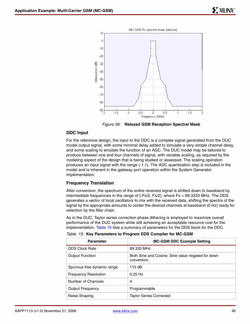
Application Example: Multi-Carrier GSM (MC-GSM)
XAPP1113 (v1.0) November 21, 2008 www.xilinx.com 46
R
DDC Input
For the reference design, the input to the DDC is a complex signal generated from the DUC model output signal, with some minimal delay added to simulate a very simple channel delay, and some scaling to emulate the function of an AGC. The DUC model may be tailored to produce between one and four channels of signal, with variable scaling, as required by the modeling aspect of the design that is being studied or assessed. The scaling operation produces an input signal with the range (-1,1). The ADC quantization step is included in the model and is inherent in the gateway port operation within the System Generator implementation.
Frequency Translation
After conversion, the spectrum of the entire received signal is shifted down to baseband by intermediate frequencies in the range of [-Fs/2, Fs/2], where Fs = 69.3333 MHz. The DDS generates a vector of local oscillators to mix with the received data, shifting the spectra of the signal by the appropriate amounts to center the desired channels at baseband (0 Hz) ready for selection by the filter chain.
As in the DUC, Taylor series correction phase dithering is employed to maximize overall performance of the DUC system while still achieving an acceptable resource cost for the implementation. Table 15 lists a summary of parameters for the DDS block for the DDC.
X-Ref Target - Figure 39
Figure 39: Relaxed GSM Reception Spectral Mask
Table 15: Key Parameters to Program DDS Compiler for MC-GSM
Parameter MC-GSM DDC Example Setting
DDS Clock Rate 69.333 MHz
Output Function Both Sine and Cosine; Sine value negated for down conversion.
Spurious free dynamic range 115 dB
Frequency Resolution 0.25 Hz
Number of Channels 4
Output Frequency Programmable
Noise Shaping Taylor Series Corrected

Application Example: Multi-Carrier GSM (MC-GSM)
XAPP1113 (v1.0) November 21, 2008 www.xilinx.com 47
R
The procedures for programming frequencies and phase offsets for the DDS are as described in the DUC section. Also as described for the DUC, the DDS sample outputs are 21-bits wide. Therefore, the 25-bit inputs to DSP48E multipliers in Virtex-5 devices are ideal for these signals.
DDC Filter Design
The MATLAB function gsm_ddc_cic_filters.m in the model subdirectory of the example is used to design the filters used in this example. See the script for details of the filter implementations described in this section.
Architectural Consideration
One of the assumptions for this example is the inclusion of a CIC filter, as DDC architecture involving FIR cascades has already been covered in XAPP1018 [Ref 1].
The general structure for the example DDC filter design echoes the corresponding DUC architecture, with the three-stage filtering process illustrated in Figure 40.
The input signal is first mixed with a sinusoid to recover the baseband signal. The CIC function is the first stage in the filter chain and provides the bulk of the total DDC rate change. The second filter provides compensation for the passband droop introduced by the CIC filter, described earlier, by enhancing the passband data with an appropriate inverse frequency function. It also commonly provides a further decimation stage, down-sampling by a factor of 2 normally. The main function of the final filter is to perform channel selection and also commonly provides a further decimation step in the down-conversion process (usually by 2). The demodulator has some influence on the overall rate change of the filter chain, as it may require an over-sampled symbol input, for timing recovery for instance.
Common Parameters and Assumptions
The input and output rates of the filter chain are important parameters in the general filter design process. The input rate of the filter chain is the mixer output rate, which is at the ADC sample conversion rate, or a small integer factor thereof. The selected rate is 256 times the symbol rate, or 69.3333 Msps, which is within the capabilities of low-cost components. For the demodulator, it is assumed that it accepts inputs at the symbol rate, which is common for GSM demodulation. The overall rate change for the DDC filter chain from ADC output to demodulator input is therefore 256.
The passband for filter design is set to 80 kHz, which is the normal GSM band of interest. It should be noted that in EDGE or Evolved EDGE systems, this might need to be wider to allow for different modulation schemes. The stopband edge is set at 100 kHz, due to the spectral mask requirements defined by the 3GPP specification at that frequency for adjacent channel interference.
The passband ripple used for specification of each filter in the cascade is set an order of magnitude less than the absolute specification for the DUC to minimize the overall ripple when the filter cascade is combined. The stopband attenuation should be specified such that the minimum requirements of the GSM channel selectivity spectral mask are met. In general, this means attenuation of at least 85 dB, plus margin to allow for earlier analog processing.
X-Ref Target - Figure 40
Figure 40: 3-Stage CIC-Based DDC Filtering
X
~
PFIR
CFIR
CIC
Mixer
Sinusoid x1113_40_101508
N 2 2
Demodulator
M

Application Example: Multi-Carrier GSM (MC-GSM)
XAPP1113 (v1.0) November 21, 2008 www.xilinx.com 48
R
CIC Filter
As with the DUC, the CIC filter is the most important filter in the chain in terms of influence on parameters and behavior of the other components in the processing chain. The CIC provides the bulk of the rate change for the DDC, and its characteristics directly determine the configuration of the CFIR filter which follows it. The PFIR filter configuration is also indirectly affected, in terms of a potential rate change, although it could be configured as a single rate filter for channel selection purposes only.
The required DDC rate change is 256, and, unlike the DUC filter chain, the PFIR filter is included. With a rate change of 2 in the CFIR and the PFIR, the rate change required in the CIC filter is set to 64. Attenuation is also a key parameter, as described in the “CIC Filter,” page 30 CIC section of the MC-GSM DUC example, and this is set to 95 dB for this example, to meet the spectral mask requirement with 10 dB of margin. This combination of parameters results in a 5-stage CIC filter, with the frequency response shown in Figure 41.
CIC Compensation Filter
The CIC compensation filter (CFIR) is a decimating low-pass FIR filter. It provides a further reduction in sample rate, to reduce the requirements on the CIC and limit the number of stages required, while also providing moderate passband filtering of the received signal (although the PFIR will be used to achieve the receive mask requirements). The CFIR also provides compensation for the passband droop introduced by the CIC filter.
The filter design script uses filter design techniques similar to those used in the DUC design to achieve the required inverse-sinc frequency response to match the CIC filter, with a decimation step being applied in this instance. As before, the filter order can be limited such that it can be implemented in a single MAC unit, in this case N=62 (63 filter taps). The attenuation in the stopband is set to 90 dB, resulting in the filter response shown in Figure 42.
X-Ref Target - Figure 41
Figure 41: Magnitude Response of CIC Filter

Application Example: Multi-Carrier GSM (MC-GSM)
XAPP1113 (v1.0) November 21, 2008 www.xilinx.com 49
R
The correction of the passband droop introduced by the CIC filter can be clearly seen in the overlay plot of the CIC, CFIR, and cascaded responses shown in Figure 43. Note that the extent of the correction required (up to 0.4 dB) is greater in this case than in the DUC, mainly due to the increase in rate change.
Pulse-Shaping Filter
The increased rate change of the CIC filter in the DDC as compared to the DUC, combined with slightly more stringent filtering requirements, necessitates the inclusion of the PFIR filtering stage. The PFIR provides an additional down-sampling factor of 2 to reduce the CIC filter requirements and provides channel selectivity according to the receive spectral mask
X-Ref Target - Figure 42
Figure 42: Magnitude Response of CFIR Filter
X-Ref Target - Figure 43
Figure 43: Passband Zoom Overlay of CIC, CFIR, and Combined Frequency Responses

Application Example: Multi-Carrier GSM (MC-GSM)
XAPP1113 (v1.0) November 21, 2008 www.xilinx.com 50
R
requirements of the GSM specification (adjacent channel interference and blocking characteristics).
The low sample rate at this stage in the processing chain allows for a high performance filter to be implemented in a single MAC unit. Therefore, a high degree of filter performance can be realized, with a filter order of up to 126 (127 filter taps). The stopband attenuation is set to 100 dB to allow for maximum blocking, meeting the mask requirements with over 10 dB of margin for additional analog processing. The resulting filter response is shown in Figure 44.
Composite Filter Response
The frequency-magnitude response of the combined filter cascade is shown in Figure 45. Both reference and quantized responses are provided.
X-Ref Target - Figure 44
Figure 44: Magnitude Response of PFIR Filter
X-Ref Target - Figure 45
Figure 45: Overall DUC Filter Response

Application Example: Multi-Carrier GSM (MC-GSM)
XAPP1113 (v1.0) November 21, 2008 www.xilinx.com 51
R
The main point to note from this response is that the most significant artifact in the stopband is due to the remnants of the first and second lobe around the first null, where the passband of the CFIR has an interpolation image. This is the performance requirement that the MATLAB CIC filter function’s attenuation parameter (described earlier) attempts to address. The interaction of the various filters can be better observed in an overlay of the frequency responses, as shown in Figure 46.
DDC Modeling and Performance
A behavioral model of the DDC was created in MATLAB, with quantization and alignment options for matching to the hardware implementation. The MATLAB script gsm_ddc_cic_model.m is in the subdirectory of the example. See this model for further detail on the modeling and performance described in this section.
The parameters relevant to the overall design are shown in Figure 16. These are grouped at the top of the script to allow for easy modification and experimentation by the interested reader. Several other parameters are calculated from these variable parameters.
X-Ref Target - Figure 46
Figure 46: Overlay of DDC Filter Responses
Table 16: Model Parameters
Parameter Description Example Default Notes
n_carr Number of carriers 4
m_duc Total rate change of DDC 256
fsym Symbol rate 1.625e6/6 Kbaud
clk_os Clock Over-sampling 4 Ratio of clock rate to sample rate; determines hardware resource sharing that can be achieved.
m_pfir Rate change of PFIR 2
m_cfir Rate change of CFIR 2
carriers Vector of carrier frequencies -0.9; -0.3;+0.3; +0.9
600 kHz carrier separation is common.
scale_vector Vector of scaling factors 1.0 (all) Optional scaling factor for each channel.

Application Example: Multi-Carrier GSM (MC-GSM)
XAPP1113 (v1.0) November 21, 2008 www.xilinx.com 52
R
The multi-carrier signal which acts as the test input to the DDC is shown in Figure 47. It is possible for users to modify this signal, perhaps to remove or scale one of the carriers, by altering the parameters of the DUC model from which it is generated and running the model to generate the data file which this model uses.
The input signal is mixed with four carriers centered at -900 kHz, -300 kHz, 300 kHz, and 900 kHz; note that the sine portion of the carrier is inverted to down-mix the channel signals. The carriers are generated by the DDS and the power spectral density of these generated carriers is plotted in Figure 48. Note that the limited sample length restricts the base noise floor, which affects both ideal and DDS generated samples. However, the two spectra are indistinguishable within that limitation. See the DDS IP core data sheet [Ref 3] for further information on DDS performance.
X-Ref Target - Figure 47
Figure 47: DDC Input Signal
X-Ref Target - Figure 48
Figure 48: PSD of DDS Generated Carriers vs. Ideal Sinusoidal Carriers

Application Example: Multi-Carrier GSM (MC-GSM)
XAPP1113 (v1.0) November 21, 2008 www.xilinx.com 53
R
PSD plots for two of the down-shifted channels (Channel 1 shifted by -900kHz; Channel 3 shifted by +300 kHz) are shown in Figure 49.
The mixer output is filtered by the CIC block defined in “CIC Filter,” providing the signal spectrum shown in Figure 50.
Note: There is some aliasing of other channel content which remains to be filtered as the CIC provides relatively poor filtering characteristics.
The output from the CIC filter is further filtered by the CFIR block defined in “CIC Compensation Filter,” page 48 [Ref 12], providing correction of the passband droop and further decimation. The output power spectral density is shown in Figure 51, along with the GSM receive mask. As can be seen, the spectrum does not yet meet the mask requirements.
X-Ref Target - Figure 49
Figure 49: Received Signal Spectra Shifted by -900 kHz and +300 kHz Carriers
X-Ref Target - Figure 50
Figure 50: CIC Filter Output Power Spectral Density

Application Example: Multi-Carrier GSM (MC-GSM)
XAPP1113 (v1.0) November 21, 2008 www.xilinx.com 54
R
To achieve the requirements of the spectral mask that is determined by the GSM specification’s adjacent channel interference and blocking characteristics, the PFIR specified in “Pulse-Shaping Filter,” page 49 is used to further filter the data. The output power spectral density is plotted in Figure 52.
DDC Implementation
The top-level block diagram for the multi-carrier GSM DDC implementation is shown in Figure 53. See the Simulink model for a more detailed view.
X-Ref Target - Figure 51
Figure 51: CFIR Output Power Spectral Density
X-Ref Target - Figure 52
Figure 52: PFIR Output Power Spectral Density

Application Example: Multi-Carrier GSM (MC-GSM)
XAPP1113 (v1.0) November 21, 2008 www.xilinx.com 55
R
Initialization
An initialization process must be performed prior to running the System Generator model simulation. The script gsm_ddc_cic_init.m must be run before using the System Generator model, as this establishes the correct environment and configuration for the System Generator model to operate. The main function of this initialization script is to run the behavioral MATLAB model to setup parameter values and generate the filter designs. The MATLAB model also generates and saves sample data (in the “results” subdirectory) for comparison with the System Generator implementation as part of the verification process for the design.
Hardware Over-Sampling
As with the DUC design, the hardware over-sampling rate is limited to four, due to r imposed by the CIC Compiler block.
Data Path Bitwidth
As with the DUC, high dynamic range of at least 96 dB is required. Therefore, 17 bits to 18 bits of data path sample width is used wherever possible.
ADC Sample Width and AGC
The ADC sample width is assumed to be 13 bits to 14 bits, which is common for modern low-cost ADC technology. Some bit-growth is assumed in analog and/or digital preprocessing (for example, AGC), resulting in 16 bits of sample width input to the mixer.
Mixer
Figure 54 shows the System Generator design of the mixer block. See the System Generator model for a more detailed view.
X-Ref Target - Figure 53
Figure 53: Top-Level Block Diagram for MC-GSM DDC Implementation
In
wr_ ch3
In
wr_ ch2
In
we3
In
we2
In
wd a ta3
In
wd a ta2
Out vo ut
sg _ yc_ dd c_ ra w
t w8
d dc_ o ut _sg
t w7
sg _sca le r_ dd c
t w6
sg _a dc _o ut pu t
t w5
sg_ yp _d dc
tw 4
sg_ yc_ dd c
tw3
sg _d o wnm i xed
t w2
sg_ yci c_ tdm
t w1
wr_ch
wdata
we
sca le r_ pr og am 1
din
ch_in
v in
wr_ch
wdata
we
dou t
ch_ou t
vou t
sca le r1
In
q _in
Out q _ch 3
Out q _ch 2
Out q _ch 1
Out q _ch 0d in
vin
do ut
ch a n_ in
cha n _o ut
vo ut
p fir_ d ec 2_ v3 _2
din_i
din_q
wr _ch
wr _data
we
m ix ed_i
mixed _q
mixed _vo ut
m ixe r
In
i _i n
Out i _c h3
Out i _c h2
Out i _c h1
Out i _c h0
d dc_ in p ut_ q
fw 2
d d c_i np u t_ i
fw 1
wr_ch
wdata
we
fr eq _ pro g am 1
din do ut
fo rm a t2
din dout
f orm a t1
↓8z -1
d nsm p le
d in
vin
d o ut
ch an _ in
c ha n_ o ut
vo ut
c fir _d ec 2_ v3 _2
din
ch _in
i_ch0
q_ch0
i_ch1
q_ch1
i_ch2
q_ch2
i_ch3
q_ch3
T DD M
T4
T 3T1
din_i
din_q
vin
dout
v out
CIC fil te rs
Sys temGe nera tor
p fir _dout
i_ ch0
q _ch0
i_ ch1
q _ch1
i_ ch2
q _ch2
p fir _vo utc fir _vou t
p fir _ch
i_ ch2
q _ch2
wr_ch
wdata
we

Application Example: Multi-Carrier GSM (MC-GSM)
XAPP1113 (v1.0) November 21, 2008 www.xilinx.com 56
R
The input data samples are captured and held for four cycles with timing arranged such that the inputs to the complex multiplier DSP slices are aligned with the DDS output channels. An alignment of channels 0 to 3 in sequence for each sample is utilized for easy understanding. The capture timing is also used to generate output validation strobes to the next stage of the DDC design.
The DDS is programmable with the user having the capability to alter the carrier frequency values by changing the frequency values in the programming block at the top level of the design.
The multiplication unit employs a complex multiplier and accumulator, constructed from DSP48 slices. This unit makes use of the dedicated cascade routing and built-in data path delay units of these DSP slices to reduce routing congestion, increase maximum speed, and reduce power consumption.
Decimating CIC Filter
The sample stream output from the mixer is suitable for direct connection to the CIC filter. The CIC filters are implemented as two modules, with one filter handling In-Phase data for the four carriers and the other handling the Quadrature data. The parameters are generally entered manually, therefore any user modification to the model must be matched manually.
The CIC filter cannot directly output an evenly spaced TDM data sample stream, as produced by other cores such as the FIR Compiler. Therefore, an adaptation module is required to convert the output from the CIC. The CIC outputs channel data on consecutive cycles until a sample has been produced for each channel. This grouped TDM channel data is buffered and converted to an evenly-spaced TDM sample stream suitable for use by the FIR filter blocks and other DSP modules. Two Distributed RAM elements and minimal logic circuitry are required to perform this function. See the CIC Compiler data sheet [Ref 2] for further information on output timing for multi-channel decimation filters, and see the System Generator model for details on the adaptation module.
X-Ref Target - Figure 54
Figure 54: Virtex-5 FPGA Mixer Implementation in System Generator
3m i xed _vo ut
2m i xe d_q
1m ixed_i
In Out1
x2zero
m ixer_cap t_q
tw2
m ixer_ca pt_i
tw1
sg_dds
tw
orz- 0
or
[a :b]
m sb3
not
inv
rei nterpret
intege ri ze _sin
rei nterpret
i nte gerize_cos
re interpre t
i nt_ q
re interpre t
i nt_i
reinterpret
dei nt_q
reinterpret
de int_i
cast
cast_v1cast
cast_v
cast
cast_si n
cast
cast_q
cast
cast_i
cast
ca st_ dinq
cast
cast_di ni
cast
cast_ cos
d
enqz- 1
cap ture_i 2
d
enqz- 1
cap ture_i 1
ab
a=bz-1
capture _en2
c1
andz- 4
and
↑4
Up Sam pl e1
↑4
Up Samp le
T 4
T 3
d qz-1
Regi ste r
P=PCIN+(A*B )
O pm ode4
P=(A*B )
O pm ode3
P=PCIN+(A*B)
Opm ode2
P=-(A*B)
Opm ode1
[ca pt_e n]
Goto
[cap t_e n]
F rom
a
b
p ci n
o p
p
DSP4 8_Q2
a
b
op
p
pco ut
DSP48_Q1
a
b
pci n
op
p
DSP48 _I2
a
b
op
p
pco ut
DSP48_I1
chann else l
da ta
we
-sin
cos
chann el
DDS Com pil er v2_0 rst out
Counter
5
we
4wr_d ata
3
wr_ch
2din_ q
1di n_i
we dds_channel
wr_data
wr_ch
dds_cos
dds_sin
i_int
q_int
din_i
din_q
Application Example: Multi-Carrier GSM (MC-GSM)
XAPP1113 (v1.0) November 21, 2008 www.xilinx.com 57
R
CFIR Filter
The implementation of the CFIR filter is a standard FIR Compiler System Generator component, using parameters (including the coefficient vector) based on MATLAB variables created by the model. Filter inputs and outputs are TDM in nature. The parameters for the core are generally defined by referencing MATLAB variables created by the model.
The coefficients of the CFIR filter are quantized by the MATLAB script already to 18-bits, with 17-bit input data width.
PFIR Filter
The implementation of the PFIR filter is also a standard FIR Compiler System Generator component based on the modeling variables. The coefficients of the PFIR filter are quantized by the MATLAB script already to 18-bits, with 17-bit input data width.
Programmable Channel Scaler
The PFIR output passes to a programmable scaler module, which allows each channel to be scaled by a different scaling factor. With the low sample rate at this point, significant resource sharing can be exploited. Therefore, a single DSP48 slice coupled with a small Distributed RAM memory are main constituents of this circuit. Interested users can adjust scale factors by opening the block mask dialog box and entering new values. Bearing in mind that the scaling of the data path is designed to handle four channels at a scaling of 1.0, quantization ranges may need adjustment should any significant increases above 1.0 be entered.
TDDM
A time division demultiplexer (TDDM) is used to deserialize the TDM channel data for input into the demodulation stage (not included in the design). The TDDM module does not include reset capability.
Synthesis
The entire DDC design can be synthesized to produce an HDL netlist, NGC netlist, or bit stream using the Output options under the System Generator token GUI interface. Synthesis is performed by the user’s preference of synthesis tool, either XST or Synplify. NGC netlist are produced by XST only (this is a Xilinx-specific netlist in binary format incorporating constraints).
System Generator also produces a project file for the Project Navigator tool from the Xilinx® ISE tool suite, which eases integration into larger designs. Using this project file, users may proceed to perform map and place and route tasks to further implement the design, or integrate with other circuits within the FPGA device. The ISE project file is created in the netlist directory specified in the System Generator token GUI, along with the design and its associated timing constraint file (XCF). It should be noted that in this particular example, when using the ISE project as created by System Generator unmodified, implementation fails initially due to an invalid timing constraint. The timing constraint is generated to handle a particular sample rate. However, no actual flip-flops operate directly in that clock enable domain. Users must modify the XCF file in the netlist directory to comment out the invalid constraint and any associated constraints which reference it, and then continue with the normal Implementation flow.
DDC Verification
The verification methodology employed for the DDC is the same as that used for the DUC design. The matching of standard MATLAB functions to hardware implementation is a convincing verification goal, providing third party validation of functional compatibility.
Verification of the DDC Sysgen implementation is performed by comparison of sample outputs at various stages in the design with those produced by the behavioral MATLAB model. The System Generator model includes several To Workspace sink blocks to direct output data samples to a MATLAB variable array for further analysis. The analyze_ddc.m script may be run after the System Generator simulation. This compares the System Generator output values

Application Example: Multi-Carrier GSM (MC-GSM)
XAPP1113 (v1.0) November 21, 2008 www.xilinx.com 58
R
with those produced by MATLAB model. Figure 55 through Figure 59 provide examples of some of the output sample traces produced by the script, demonstrating the bit-accurate matching of the data samples.X-Ref Target - Figure 55
Figure 55: Comparative Analysis of Down-Mixed Signal, Channel 1
X-Ref Target - Figure 56
Figure 56: Zoom of Down-Mixed Signal Comparison, Channel 1

Application Example: Multi-Carrier GSM (MC-GSM)
XAPP1113 (v1.0) November 21, 2008 www.xilinx.com 59
R
X-Ref Target - Figure 57
Figure 57: Comparative Analysis of CIC Output Results
X-Ref Target - Figure 58
Figure 58: Comparative Analysis of CFIR Output Results

Application Example: Multi-Carrier GSM (MC-GSM)
XAPP1113 (v1.0) November 21, 2008 www.xilinx.com 60
R
The signals match for all stages. Note that, as with the DUC, the DDS function in the bit-accurate model is a recorded sample stream. However, the maturity of the DDS and the extensive verification and validation performed on that core mean that this is not regarded as a significant factor in achieving confidence in the design’s functional correctness.
DDC Resource Utilization
The DUC design was synthesized and targeted at a Virtex-5 device, XC5VSX50T, -1 speed grade, in an FF665 package. The estimated resource utilization of the DUC is summarized in Table 17.
The implementation of the CIC filters in the design does not use DSP slices by default, but an option is provided to users to prefer DSP slice utilization. For this configuration, the resource utilization is summarized in Table 18.
X-Ref Target - Figure 59
Figure 59: Comparative Analysis of PFIR Output Results
Table 17: Resource Utilization of 4-carrier GSM DDC
Resource Type Number Required
DSP48Es 9
Block RAM 2
LUT-FF pairs 2694
LUTs 1964
FFs 2571
Table 18: Resource Utilization of 4-carrier GSM DDC Using DSP Slices for CIC
Resource Type Number Required
DSP48Es 21
Block RAM 2
LUT-FF pairs 2361
LUTs 1566
FFs 2175

Application Example: Multi-Carrier GSM (MC-GSM)
XAPP1113 (v1.0) November 21, 2008 www.xilinx.com 61
R
Note: Only around 330 LUT-FF pairs are saved by this option, roughly equivalent to 80 slices depending on packing and configuration, while an extra 12 DSP slices are required. This trade-off is almost certainly not beneficial, although power consumption should be considered.
DDC Power Consumption
The estimated power consumption of the Virtex-5 FPGA DDC design, using the XPower Analyzer tool, is summarized in Table 19 and Table 20.
Note: The option of using DSP48 slices to implement the CIC filters results in higher power consumption in this case. Combined with the meager saving in slices and the larger increase in DSP slices shown above, the CIC configuration using logic rather than DSP slices is the better choice in this case.
Limitations of CIC-Based DDC Implementation
As with the DUC design, flexibility in terms of sample rates is one of the main limitations of a CIC-based DDC implementation, and the comments made in “Limitations of CIC-based DUC Implementation” apply here once more. The selection of the sample rate at which to perform multi-carrier mixing is restricted by the bulk rate change of the CIC filter, while for advanced systems, with support for multiple symbol rates and multiple air standards, some adaptation and merging of sample rates is likely to be required, which is better suited to a FIR-based structure.
Table 19: Power Consumption of 4-Carrier GSM DDC Using Logic Slices for CIC
Power Type Power Value (W)
Quiescent (static) power 0.58994
Dynamic power 0.21136
Total power 0.80130
Table 20: Power Consumption of 4-carrier GSM DDC using DSP slices for CIC
Power Type Power Value (W)
Quiescent (static) power 0.59203
Dynamic power 0.23942
Total power 0.83145

Application Example: Multi-Channel MRI Receiver
XAPP1113 (v1.0) November 21, 2008 www.xilinx.com 62
R
Application Example: Multi-Channel MRI Receiver
Medical imaging systems often employ digital down-converters to translate detected signals from a wide sampled band down to a narrow band for analysis. Magnetic Resonance Imaging (MRI) equipment requires detection, frequency translation, and filtering of the Free-Induction Decay (FID) signals in the RF band, down-converting to baseband for interpretation and analysis. Replacing analog signal processing with digital equivalents as early as possible in the processing chain can provide a significant reduction of the overall system cost and smaller power consumption. Results are also more predictable as they are less susceptible to environmental considerations. This application example shows how the digital down-conversion (DDC) function can be efficiently implemented in a Xilinx® FPGA devices, both in terms of resources and power consumption.
This example describes a method for building a model and hardware implementation of a multi-channel down-converter. A combination of Simulink blocks and MATLAB scripts is used to control the hardware and collect and display the results with a minimum of user interaction. This provides a simple mechanism for the user to control all aspects of the system, including the capability to automatically measure MRI Digital Down Converter (DDC) performance with many different combinations of parameters. The example includes:
• Easy to understand and highly parameterizable MATLAB scripts that generate the model
• Scripts that generate a Sysgen schematic that implements the model
• Automated test bench creation and verification of the results
• Analysis of DDC performance in terms of resource utilization and power consumption.
Design Files
The design files are listed in Table 21. These are MATLAB script files which automatically generate the example design.
The easiest way for readers to familiarize themselves with the example is to copy all the files to an empty directory, start MATLAB, and then run the mri_top.m script. The result will be an mri.mdl System Generator model file that is generated in the same directory. In a newly created netlist subdirectory, there will be a new ISE project file alongside the necessary netlists and source files for the design.
Although it is advisable to read through the example description beforehand, users may quickly get started and explore the design by following the steps described below.
To get started:
1. Create a new working directory in MATLAB with System Generator installed, and copy all the .m files into it.
2. Run mri_top.m script. This script first builds a model, then runs it, and finally runs a System Generator script that generates a filter with the same parameters as the model and with maximum possible number of the input channels. The comments in the mri_top.m script describe what each line is doing, and the script may be run line by line to allow the user to follow progress and understand each step in turn. The output of the script is the
Table 21: MRI example design files
File Description
mri_top.m Top-level script that calls model and then generates a System Generator netlist based on the MRI parameters.
mri_model.m Signal generation and analysis.
mri_filter_model.m MATLAB filter generation.
mri_filter_netlist.m Netlist generator.
mri_verify.m Verification script.

Application Example: Multi-Channel MRI Receiver
XAPP1113 (v1.0) November 21, 2008 www.xilinx.com 63
R
mri.mdl System Generator model file, a few filter response graphs, and spectral plots of a test signal after each major processing stage.
To compare the model results and System Generator implementation results, an additional step is needed:
3. Run mri_verify.m script. This outputs the final spectrum of the test signal after processing by the model and by hardware implementation.
Application Overview
Magnetic Resonance Imaging (MRI) is a medical imaging technique for obtaining high resolution three-dimensional images of tissue structures by measuring emission of the selectively excited nuclei in the tissues. MRI provides much greater contrast between the different soft tissues of the body than does computer tomography (CT), making it especially useful in neurological, musculoskeletal, cardiovascular and oncological imaging.
The basic operation of MRI systems can be summarized as follows. The subject to be imaged is placed in a large highly uniform magnetic field, which is normally created by passing a current through a superconducting material. Since some nuclei have an overall spin (odd number of protons/neutrons), they are effectively dipoles, which align to the magnetic field. Particular regions and types of nuclei within the subject are selected for excitation by application of a static magnetic gradient along one of the axes and then application of variable magnetic gradients along the other axes. RF energy at a specific frequency is then transmitted into subject for a short pulse duration (2 ms to 10 ms) via an RF coil. The energy perturbs the nuclei in their alignment with magnetic field, due to nuclear magnetic resonance at that specific frequency. After the RF transmitter is switched off once more, the nuclei precess back into alignment with the static field. This decay of the nuclei within the subject from one energy state to another releases the induced energy as a re-transmitted RF signal with a particular signature (known as the Free Induction Decay, or FID). The detected RF signal can then be reconstructed into an image. Field gradients, pulse timing and other parameters can be adjusted to produce different modulation effects on the FID.
The FID response emissions are measured by a collection of coils located near the patient’s body. The number of coils in the latest models can reach 128 or more, located in custom-made enclosures around the body part of interest or clothing (e.g., a vest) which the patient wears during the scan. This multitude of channels presents an ergonomic problem, that of passing all the signals to the processing equipment. And thus, packing multiple channels into a single cable is beneficial.
A fundamental characteristic of MRI systems is the nuclear magnetic resonance frequency (or Larmor frequency). The FID emission occurs in a narrow spread of frequencies of 5 kHz to
X-Ref Target - Figure 60
Figure 60: MRI Scanner Equipment

Application Example: Multi-Channel MRI Receiver
XAPP1113 (v1.0) November 21, 2008 www.xilinx.com 64
R
500 kHz centered around the Larmor frequency, which is dependent primarily upon the atom of interest (in most production systems this is hydrogen, due to the prevalence of the hydrogen nucleus in body tissues, particularly water, and its high NMR response). The other main parameter affecting the Larmor frequency is the strength of the magnetic field, Bo, upon which it is linearly dependent. For example, in a 1.5T system, the Larmor frequency for hydrogen is approximately 67 MHz. The Larmor frequencies for each type of nuclei are calculated as:
Equation 3
γ is the gyromagnetic ratio, or Larmor constant, which is a characteristic of each target molecule. For the hydrogen atom (or more correctly, for the single proton nucleus), this constant is approximately 42.57 MHz/T. The gyromagnetic ratios for other nuclei are shown in Table 22.
Digital Down-Converter
Architectural Consideration
An important distinction when comparing down-conversion in MRI systems to down-conversion in communications systems is that channels in MRI systems have similar frequency profiles, as the basic Larmor frequencies for each physical channel are the same. In other words, the channels are spatially separate rather than separated in the frequency domain. Therefore, the multi-channel FDM techniques used in communications systems are not appropriate.
For this example, it is assumed that the data are sampled by an analogue-digital converter (ADC) immediately after the preamplifier, as is schematically shown in Figure 61.
Table 22: Gyromagnetic Ratios for Different Nuclei
Nucleus γ (MHz/T)1H 42.576
3He -32.4347Li 16.54613C 10.70514N 3.076615N -4.315617O -5.7716
23Na 11.26231P 17.235
129Xe -11.777
X-Ref Target - Figure 61
Figure 61: MRI Pre-amplifier and Converter Context
πγ2
0Bf =
Op Amp
DDS
CIC CFIR
Analog FPGA

Application Example: Multi-Channel MRI Receiver
XAPP1113 (v1.0) November 21, 2008 www.xilinx.com 65
R
For down-conversion, the input data sample sequence is multiplied by an internally generated sine wave (corresponding to the base Larmor frequency, and common for all channels) and then down-sampled through a filter block. The down sampling rate R can be estimated as:
Equation 4
where fADC is input sampling rate, fspread is the anticipated Larmor frequency spread and k is a over-sampling factor greater than 2. For the purposes of this example, the over-sampling factor is selected as 8. The trade-off in selecting k is that larger values lead to higher quality of the signal. However, due to the increased sampling rates, the amount of the hardware required for the CFIR and any subsequent processing blocks increases.
After the mixing stage, the CIC low pass decimation filter reduces the sampling rate, while applying moderate anti-aliasing filtering. Since the signal passband spectrum is distorted by passband droop in the CIC filter, a CFIR is required to correct this. This low-pass compensation filter also provides further rate reduction by decimating by 2 and reduces high-frequency noise.
Performance Requirements
The typical performance requirements of the DDC implementation for MRI are summarized in Table 23. The example DDC design has been implemented with a great deal of flexibility to accommodate variation of these parameters.
Input
A test signal was created for the DDC test bench that represents the type of signal one might expect to detect as an MRI FID emission. Other test signals may be applied to the DDC design input, but no other test signals were explicitly tested in this example. For acceptable measurement of performance within a reasonable time period, a few rules should be followed when generating this test signal. In the model, the length of the sample Ns is the power of two closest to
Table 23: Typical DDC Requirements for MRI
Parameter Value Comments
Band of interest 25-500 kHz Tunable.
Carrier separation 0 kHz Same Larmor frequency.
Static Magnetic Field Strength 1.5 Teslas Typical field strength in current MRI systems.
Larmor frequency 63.855 MHz Derived from magnetic field strength, assuming hydrogen nuclei are targeted.
Channels 16 to 128 Typical range of physical channels in modern equipment.
Input Signal Quantization 12 to 16 bits, real Depends on ADC and conversion rate.
Output Signal Quantization 16-bits I & Q High dynamic range required.
Mixer Tunability Variable Allows different nuclei to be targeted.
Mixer Resolution 0.25 Hz 28 bits of phase accumulator width.
Mixer SFDR 115 dB Various SFDR options are available in the DDS Compiler core.
spread
ADC
fkfR×
=
fadc fres×fspread
-------------------------

Application Example: Multi-Channel MRI Receiver
XAPP1113 (v1.0) November 21, 2008 www.xilinx.com 66
R
where fadc is the ADC sample conversion rate, fres is the required spectrum resolution (i.e., the number of FFT bins that should fall within Larmor frequency spread), and fspread is the Larmor frequency spread. This length of test signal is necessary to get reasonable spectral resolution of the output signal, while the power of two provides faster FFT analysis.
When a test signal is generated, the spectrum of the test signal is calculated first, such that there would be no mismatch between the sample signal’s FFT bins and the desired harmonics. The easiest way of ensuring this is to build the test signal as a sum of sine or cosine waves each of the frequency of one of the bins of the FFT image of the input signal.
The other important parameter for the test signal is the frequency shift in the mixer. To avoid mismatch between the FFT bin location and the harmonics of the shifted signal, the frequency shift is selected such that it would be an integer multiple of
Modeling
The MATLAB script mri_model.m implements the model of the MRI system. It uses parameters that are set up by the mri_top.m script file. The main parameters of the model are described in Table 24.
There are a number of other configurable parameters in the model that do not affect the generated hardware, but do affect the design flow, output formats, and measurements. These are not listed here, but experienced users may wish to alter these to suit their particular circumstances.
The outputs of the model are:
• Filtered and down-sampled version of the input signal(s)
• Filter response plots
• Filter parameters (for subsequent use in System Generator filter implementation)
Table 24: MRI DDC model parameters
Parameter Description
fadc Sample rate of the analog-to-digital converter. Since this frequency has to be reasonably high, the clock frequency is assumed to be the same (more than 150 MHz).
flarmor Larmor frequency of interest, which depends on the system’s constant magnetic field and the type of nuclei being studied.
fwidth Spectral width of Larmor frequency distribution. This distribution is caused by the variable magnetic field gradients and by chemical shift and thus can vary significantly, but generally it is several orders of magnitude smaller than the base Larmor frequency.
input_adc_bitwidth ADC sample bitwidth, with sample values being treated as signed values in the range (-1,1).
internal_bitwidth Width of the internal fixed point data representation, used for intermediate computation results and output values.
internal_fixed_point Position of the fixed point in the internal data representation.
available_input_pins Number of pins of the FPGA available to provide ADC input sample values. For multi-channel designs, the number of the pins available may be a significant and limiting factor, and the maximum number of channels that may be implemented takes this value into account.
fstep
fadc
Ns----------=

Application Example: Multi-Channel MRI Receiver
XAPP1113 (v1.0) November 21, 2008 www.xilinx.com 67
R
The model also instantiates a few structures and variables that later are used by the System Generator script.
Filter Design
Filter generation is performed by the function mri_filter_model.m, which is called automatically from the model scripts. The function generates two filters: the Cascaded Integrator-Comb (CIC) filter and the Compensation Finite Impulse Response (CFIR) filter. For generating both of these filters, standard MATLAB functions such as fdesign() are used.
CIC Filter
The first stage, the CIC filter, is used for down-rating the down-mixed signal as much as possible. The attenuation of the filter determines the number of stages in the CIC, which is the main variable parameter for this system. The frequency response of one of many possible configurations for the CIC filter in the example design is shown in Figure 62.
As described previously, CIC filters exhibit a sinc-like frequency response, which can result in passband droop. This passband droop normally must be corrected to allow faithful signal reconstruction of the down-converted signal, therefore, a compensation filter is required.
CIC Compensation Filter
The Compensation FIR filter, or CFIR, is generated by the MATLAB filter generation function with an inverse-sinc frequency response profile such that it matches the CIC in terms of number of stages. When the two filters are cascaded, the resulting filter response should have a flat plateau at low frequency. The CFIR filter also provides a further decimation of the sample stream by a factor of 2, and some low-pass filtering for anti-aliasing and signal-to-noise ratio improvement. An example of the shape of the frequency response for a typical CFIR configuration is shown in Figure 63.
X-Ref Target - Figure 62
Figure 62: MRI DDC CIC Frequency Response
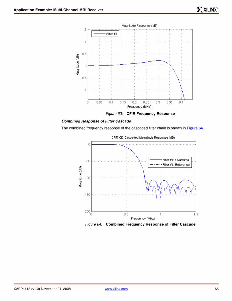
Application Example: Multi-Channel MRI Receiver
XAPP1113 (v1.0) November 21, 2008 www.xilinx.com 68
R
Combined Response of Filter Cascade
The combined frequency response of the cascaded filter chain is shown in Figure 64.
X-Ref Target - Figure 63
Figure 63: CFIR Frequency Response
X-Ref Target - Figure 64
Figure 64: Combined Frequency Response of Filter Cascade

Application Example: Multi-Channel MRI Receiver
XAPP1113 (v1.0) November 21, 2008 www.xilinx.com 69
R
The correction of the CIC response in the passband that is provided by the CFIR is illustrated by Figure 65.
Frequency Translation
Frequency translation is achieved by multiplication of a sinusoidal function (generated by the DDS block) and the input sample stream. Only a single DDS output is required to handle all channels, as they are spatially separated rather than spectrally.
There is a tradeoff between using a complex multiplication (i.e., multiplying by both sine and cosine) which requires processing of complex values and multiplying with only a sine function. This results in purely real computations. Keeping all the computations as real values significantly reduces the amount of hardware required (by factor of nearly two), which is particularly important for multi-channel implementation, where the down-sampling ratio is large and where the number of channels is limited by the hardware available. The downside of all-real computation is that after detection the signal spectrum must stay positive to avoid aliasing.
Multiplying the input data by complex value exp(-jωt) provides a signal band that is half as narrow at the output stage, but which requires more computation (twice as many for the majority of the operations required). Still, the benefit of increasing the down-sampling ratio may be significant in some cases.
For simplicity, this example describes all-real implementation.
Implementation
System Generator was chosen as the implementation tool for this example because of the close integration with MATLAB, which allows close coupling of the MATLAB behavioral model with the equivalent hardware implementation. Netlist generation and verification of the system can also be performed within the same environment. Using System Generator’s scripting capabilities, a netlist can be constructed for a DSP design from class-leading DSP IP cores that matches the modeled performance and meets customer requirements.
The flow consists of the following stages:
1. Generate a model with user-defined parameters such as
a. Input (ADC) sampling frequency;
b. Larmor frequency and Larmor frequency spread;
c. Number of input pins available;
X-Ref Target - Figure 65
Figure 65: Passband Zoom of Compensated Frequency Response

Application Example: Multi-Channel MRI Receiver
XAPP1113 (v1.0) November 21, 2008 www.xilinx.com 70
R
d. ADC and internal fixed point data precision.
2. Generate a netlist that matches the model’s specified parameters. This controls:
a. Filter (FIR Compiler and CIC Compiler) parameters;
b. Number of channels;
c. Sine/cosine signal generation (DDS Compiler properties).
3. Run a test bench to ensure the bit accuracy of the MATLAB model to the netlist.
This step may be deprecated in simple cases where the design uses only pre-verified IP cores.
4. Generate an XST project and then implement the FPGA circuit:
a. Map
b. Place and Route
c. Xpower analysis
d. Resource utilization
e. Bitstream Generation
5. Run model to measure the system characteristics such as:
a. Signal-to-noise ratio (SNR)
b. Filter response and attenuation
Other than the Xilinx ISE back-end flow, which is scripted and automated, everything can be done within the MATLAB environment either manually or by running mri_top.m script.
System Generator allows the user to implement a design both through manual input and via a script. The advantage of an M-code script is that it allows designers to fully reuse the results of the simulation and build a model that is an exact (or sufficiently close to) bit-accurate match to the model.
Single Channel
The single channel implementation consists of a DDS block that generates a sine wave, a mixer (multiplier), the CIC filter, and the CFIR filter. Between the CIC and the CFIR, some data trans-formation is needed to adjust the apparent sample rate, as the CIC Compiler block for System Generator requires data inputs and outputs to operate at the clock rate. It is often advisable to convert CIC filter input values to integer representation, as the CIC Compiler block introduces significant gain, which, after truncation to a sensible bitwidth, may push the fixed point below the LSB of the output representation, which is not supported in System Generator. The output of course will need to be re-interpreted also. Note that this requires no additional resources and requires only a change in fixed-point number representation. This integer conversion is per-formed by default by the example model script and System Generator implementation. The schematic for a single channel is shown in Figure 66.
Scaling of the CIC filter’s output is required to convert the integer values it uses into fixed-point representation (again, this latter step does not infer any logic generation). A capture register, with the enable controlled by the RDY signal output from the CIC filter is also added. This holds the desired output sample value stable for the entire down-sampled period (otherwise, the out-put changes each clock cycle as output sample values are computed). The down-sample block is there to convert the sampling rate to the appropriate rate at that stage in the data path for input to the CFIR. The additional circuitry does lead to some small resource increase (which is potentially unnecessary).
When the System Generator implementation is simulated, the result is stored in mri_model_output variable in the MATLAB workspace.
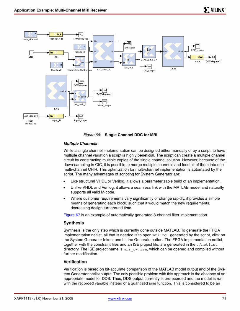
Application Example: Multi-Channel MRI Receiver
XAPP1113 (v1.0) November 21, 2008 www.xilinx.com 71
R
Multiple Channels
While a single channel implementation can be designed either manually or by a script, to have multiple channel variation a script is highly beneficial. The script can create a multiple channel circuit by constructing multiple copies of the single channel solution. However, because of the down-sampling in CIC, it is possible to merge multiple channels and feed all of them into one multi-channel CFIR. This optimization for multi-channel implementation is automated by the script. The many advantages of scripting for System Generator are:
• Like structural VHDL or Verilog, it allows a parameterizable build of an implementation.
• Unlike VHDL and Verilog, it allows a seamless link with the MATLAB model and naturally supports all valid M-code.
• Where customer requirements vary significantly or change rapidly, it provides a simple means of generating each block, such that it would match the new requirements, decreasing design turnaround time.
Figure 67 is an example of automatically generated 8-channel filter implementation.
Synthesis
Synthesis is the only step which is currently done outside MATLAB. To generate the FPGA implementation netlist, all that is needed is to open mri.mdl generated by the script, click on the System Generator token, and hit the Generate button. The FPGA implementation netlist, together with the constraint files and an ISE project file, are generated in the ./netlist directory. The ISE project name is mri_cw.ise, which can be opened and compiled without further modification.
Verification
Verification is based on bit-accurate comparison of the MATLAB model output and of the Sys-tem Generator netlist output. The only possible problem with this approach is the absence of an appropriate model for DDS. Thus, DDS output currently is prerecorded and the model is run with the recorded variable instead of a quantized sine function. This is considered to be an
X-Ref Target - Figure 66
Figure 66: Single Channel DDC for MRI

Application Example: Multi-Channel MRI Receiver
XAPP1113 (v1.0) November 21, 2008 www.xilinx.com 72
R
acceptable method, as the performance of the DDS block is well documented and the core is well verified.
Validation of the design is achieved by comparing input and output spectrum. The output spec-trum should match the input within the acceptable error limits and while it has to be shifted into the desired frequency bandwidth.
The provided script, mri_verify.m, compares the result of the System Generator implemen-tation and MATLAB model output and reports any differences between them. The plots that are present by the script show the spectra of the System Generator and MATLAB output signals both in absolute and logarithmic scale.
Resource Utilization
Resource utilization depends on a variety of parameters, such as number of channels, data bit width, and so on. Therefore, the data in Table 25 should be used only as an indication.
When the down-sampling rate of the CIC filter is large, the FIR Compiler block can implement a multi-channel compensation filter that processes more than one CIC output. This leads to a reduction both in resource requirements and power consumption per channel (since the CFIR block is shared to a higher degree). The number of channels to be multiplexed prior to the CFIR filter input is defined by the down-sampling rate, which depends on the ratio of the Larmor frequency and the spread of frequencies present in the signal of interest. The maximum number of channels may also be limited by available hardware resources, such as I/Os and DSP48 blocks on the particular device.
Individual Channel Implementation
Individual channel implementation is used when the down-sampling rate in the CIC filter is not big enough to combine several channels into one compensation filter (CFIR). In this case, multiple copies of the single channel implementation are used to implement the required number of channels. Resource utilization in a Virtex-5 FPGA per channel is:
If more than one channel is being implemented in the same chip, the DDS block can be shared, which will lead to reduced resource utilization per channel.
Table 25: Individual Channel Resource Utilization (per channel)
Resource Type Number Required
DSP48Es 9Block RAM 1
LUT-FF pairs 579LUTs 307FFs 571

Application Example: Multi-Channel MRI Receiver
XAPP1113 (v1.0) November 21, 2008 www.xilinx.com 73
R
X-Ref Target - Figure 67
Figure 67: 8-Channel DDC for MRI

Application Example: Multi-Channel MRI Receiver
XAPP1113 (v1.0) November 21, 2008 www.xilinx.com 74
R
Multi-Channel Implementation
In multiple channel implementation, both the DDS and the compensation filter can be shared due to significant down-sampling in the CIC filters. This leads to smaller resource per channel requirements, and often the number of IO pins available becomes the limiting factor. Since the highest ratio of IO/logic is in the smallest chips, the most efficient multi-channel implementation may be in the smallest chip available. The maximum number of 14-bit channels in the smallest XC5VSX35T, in an FF665 package, is 21 per chip. The resource consumption for this implementation is shown in Table 26.
This provides a good balance with the number of DSP48E blocks available, and the reduction of the input data bitwidth does not lead to an increase in the number of implementable channels even if the down-sampling rate allows it.
Power Consumption
The power consumption figures consist of two main values: static power and dynamic power per channel. The XPower Analyzer was used to provide the following estimates.
Individual Channel Implementation
For a single channel configuration in XC5VSX35T, in an FF665: package, -1 speed grade, the power consumption per channel is shown in Table 27.
When more than one channel is implemented by replication, Dynamic power increases linearly with the channel count. It is likely that the static power will also increase, but not linearly and significantly less than the dynamic power.
Multi-channel Implementation
The power consumption also increases with the number of channels, but not proportionally; rather, it increases more or less proportionally to the increase in resource utilization, as might be expected. Thus, the power consumption figures for 21-channel implementation on the same chip as above are shown in Table 28.
Table 26: Resource Utilization for 21-Channel Implementation
Resource Type Number Required
DSP48Es 170
Block RAMs 4
LUT-FF pairs 8992
LUTs 2780
FFs 8667
Table 27: Power Consumption for Individual Channel Implementation (per channel)
Power Type Power Value (W)
Quiescent (static) power 0.37440
Dynamic power 0.05546
Total power 0.42986
Table 28: Power Consumption for 21-Channel Implementation
Power Type Power Value (W)
Quiescent (static) power 0.39246
Dynamic power 0.44456
Dynamic power per channel 0.02117

Conclusion
XAPP1113 (v1.0) November 21, 2008 www.xilinx.com 75
R
The multi-channel implementation structure described is, therefore, a highly efficient method of implementing down-conversion for modern multi-channel MRI systems.
Conclusion The examples provided by this application note demonstrate how Xilinx® FPGAs can be combined with powerful DSP tools and class-leading IP cores to implement designs for narrowband DSP systems in a varied range of applications. The realized designs are efficient both in terms of resources and of power, taking advantage of the advanced features of Xilinx devices and the high performance of its DSP IP cores.
Two approaches to design creation and verification have been presented. Firstly, a manual schematic creation approach, with verification by bit-accurate matching to a behavioral MATLAB model. Secondly, an automated scripted schematic generation approach, with verification by comparison of results against functional requirements. Each has its advantages and disadvantages. However, these approaches are not mutually exclusive and many of the merits of both may be merged into the same design flow.
As the optimal solution for any given application varies, the application note highlights some of the most significant parameters that affect the design process, and the reasons which drive the choices the designer must make. The example designs have been created with this in mind and are readily adapted to suit specific system requirements. The techniques may also be combined with those described in [Ref 1], which describes FIR-based DUC/DDC designs, to create a custom solution for a chosen application and its requirements.
References 1. Tarn, H., et al, Designing Efficient Wireless Digital Up and Down Converters Leveraging CORE Generator and System Generator, Xilinx® Application Note, XAPP1018,
2. Xilinx® CIC Compiler, http://www.xilinx.com/products/ipcenter/CIC_Compiler.htm
3. Xilinx® DDS Compiler, http://www.xilinx.com/products/ipcenter/DDS_Compiler.htm
4. Xilinx® FIR Compiler, http://www.xilinx.com/products/ipcenter/FIR_Compiler.htm
5. Xilinx® ISE Design Suite 10.1 Software Manuals, http://www.xilinx.com/support/software_manuals.htm
6. Hogenauer, E., An Economical Class of Digital Filters for Decimation and Interpolation, IEEE Transactions on Acoustics, Speech, and Signal Processing, vol. ASSP-29, no. 2, April 1981.
7. Lyons, R., Understanding Cascaded Integrator-Comb Filters, Embedded Systems Design, March 2005.
8. Analog Devices, Multi-Carrier GSM with State of the Art ADC technology, White Paper, October 2007 (revision).
9. Maxim Integrated Circuits, Digital-to-Analog Converters (DACs) for High-Performance Communications, Application Note 3176, April 2004.
10. Xilinx®, PC-CFR Reference Design.
11. Xilinx®, Digital Predistortion Reference Designs, Product Note 2061.
12. 3GPP, Radio Transmission and Reception, Technical Specification 45.005, v7.12.0, November 2007.
13. Linz, A., Efficient Implementation of an I-Q GMSK Modulator, IEEE Trans. Circuits and Systems, Vol. 43, No. 1, January 1996.
Total power 0.83702
Total power per channel 0.03986
Table 28: Power Consumption for 21-Channel Implementation (Cont’d)
Power Type Power Value (W)

Revision History
XAPP1113 (v1.0) November 21, 2008 www.xilinx.com 76
R
14. Vankka, J. & Honkanen, M., A Multi-Carrier GMSK Modulator, IEEE Journal on Selected Areas in Communications, vol. 19, no. 6, June 2001.
15. Agilent Technologies, Measuring EDGE Signals, Application Note 1361.Agilent Technologies, Measuring EDGE Signals, Application Note 1361.
Revision History
The following table shows the revision history for this document:
Notice of Disclaimer
Xilinx is disclosing this Application Note to you “AS-IS” with no warranty of any kind. This Application Note is one possible implementation of this feature, application, or standard, and is subject to change without further notice from Xilinx. You are responsible for obtaining any rights you may require in connection with your use or implementation of this Application Note. XILINX MAKES NO REPRESENTATIONS OR WARRANTIES, WHETHER EXPRESS OR IMPLIED, STATUTORY OR OTHERWISE, INCLUDING, WITHOUT LIMITATION, IMPLIED WARRANTIES OF MERCHANTABILITY, NONINFRINGEMENT, OR FITNESS FOR A PARTICULAR PURPOSE. IN NO EVENT WILL XILINX BE LIABLE FOR ANY LOSS OF DATA, LOST PROFITS, OR FOR ANY SPECIAL, INCIDENTAL, CONSEQUENTIAL, OR INDIRECT DAMAGES ARISING FROM YOUR USE OF THIS APPLICATION NOTE.
Date Version Description of Revisions
11/21/08 1.0 Initial Xilinx release.