Embed Size (px)
Citation preview
TIDA-00716 - Test ReportXilinx® Spartan® 6 Power Reference Design with TPS650250 Power Management IC 1
Copyright © 2015, Texas Instruments Incorporated
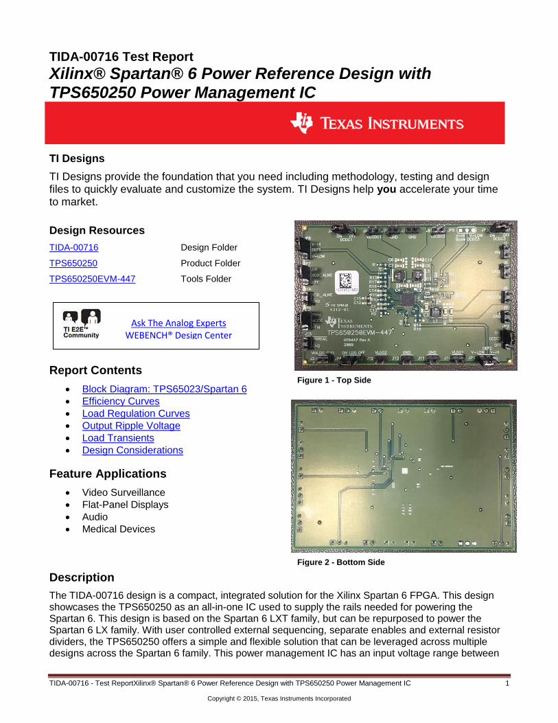
TIDA-00716 Test Report
Xilinx® Spartan® 6 Power Reference Design with TPS650250 Power Management IC
TI Designs
TI Designs provide the foundation that you need including methodology, testing and design files to quickly evaluate and customize the system. TI Designs help you accelerate your time to market.
Design Resources
TIDA-00716 Design Folder
TPS650250 Product Folder
TPS650250EVM-447 Tools Folder
Report Contents
Block Diagram: TPS65023/Spartan 6
Efficiency Curves
Load Regulation Curves
Output Ripple Voltage
Load Transients
Design Considerations
Feature Applications
Video Surveillance
Flat-Panel Displays
Audio
Medical Devices
Description
The TIDA-00716 design is a compact, integrated solution for the Xilinx Spartan 6 FPGA. This design showcases the TPS650250 as an all-in-one IC used to supply the rails needed for powering the Spartan 6. This design is based on the Spartan 6 LXT family, but can be repurposed to power the Spartan 6 LX family. With user controlled external sequencing, separate enables and external resistor dividers, the TPS650250 offers a simple and flexible solution that can be leveraged across multiple designs across the Spartan 6 family. This power management IC has an input voltage range between
Ask The Analog Experts WEBENCH® Design Center
Figure 1 - Top Side
Figure 2 - Bottom Side
TIDA-00716 – Test ReportXilinx® Spartan® 6 Power Reference Design with TPS650250 Power Management IC 2
Copyright © 2015, Texas Instruments Incorporated
3.5 and 5.5V and can be run from a 5V supply or a single cell Li-Ion battery. This design has been tested and verified for industrial applications (-40°C to 85°C).
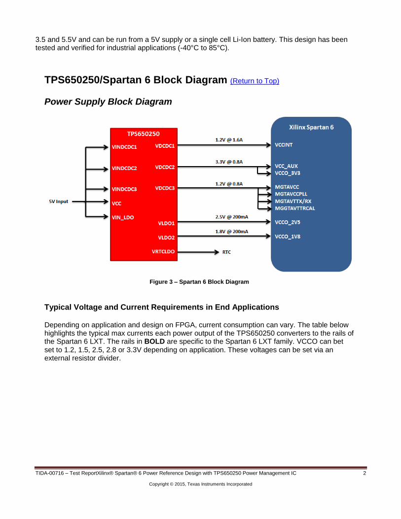
TPS650250/Spartan 6 Block Diagram (Return to Top) Power Supply Block Diagram
Figure 3 – Spartan 6 Block Diagram
Typical Voltage and Current Requirements in End Applications Depending on application and design on FPGA, current consumption can vary. The table below highlights the typical max currents each power output of the TPS650250 converters to the rails of the Spartan 6 LXT. The rails in BOLD are specific to the Spartan 6 LXT family. VCCO can bet set to 1.2, 1.5, 2.5, 2.8 or 3.3V depending on application. These voltages can be set via an external resistor divider.
www.ti.com
TIDA-00716 – Test ReportXilinx® Spartan® 6 Power Reference Design with TPS650250 Power Management IC 3
Copyright © 2015, Texas Instruments Incorporated
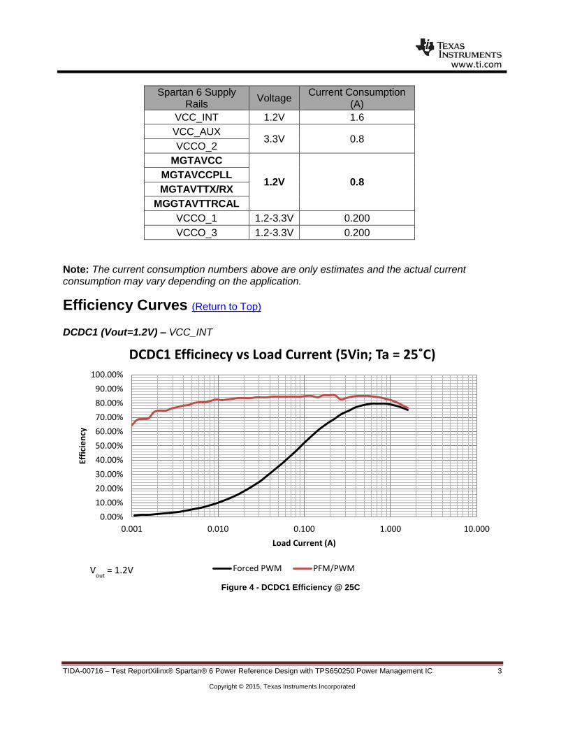
Spartan 6 Supply Rails
Voltage Current Consumption
(A)
VCC_INT 1.2V 1.6
VCC_AUX 3.3V 0.8
VCCO_2
MGTAVCC
1.2V 0.8 MGTAVCCPLL
MGTAVTTX/RX
MGGTAVTTRCAL
VCCO_1 1.2-3.3V 0.200
VCCO_3 1.2-3.3V 0.200
Note: The current consumption numbers above are only estimates and the actual current consumption may vary depending on the application.
Efficiency Curves (Return to Top) DCDC1 (Vout=1.2V) – VCC_INT
Figure 4 - DCDC1 Efficiency @ 25C
0.00%
10.00%
20.00%
30.00%
40.00%
50.00%
60.00%
70.00%
80.00%
90.00%
100.00%
0.001 0.010 0.100 1.000 10.000
Effi
cie
ncy
Load Current (A)
DCDC1 Efficinecy vs Load Current (5Vin; Ta = 25˚C)
Forced PWM PFM/PWMVout
= 1.2V
www.ti.com
TIDA-00716 – Test ReportXilinx® Spartan® 6 Power Reference Design with TPS650250 Power Management IC 4
Copyright © 2015, Texas Instruments Incorporated
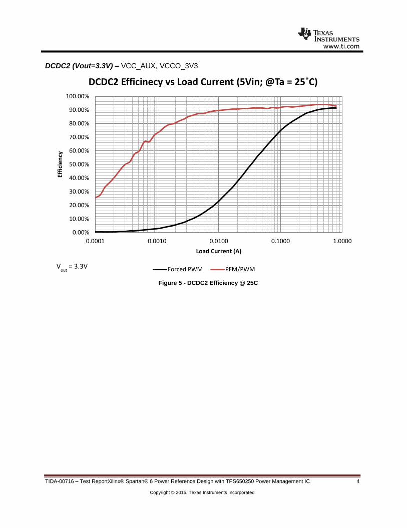
DCDC2 (Vout=3.3V) – VCC_AUX, VCCO_3V3
Figure 5 - DCDC2 Efficiency @ 25C
0.00%
10.00%
20.00%
30.00%
40.00%
50.00%
60.00%
70.00%
80.00%
90.00%
100.00%
0.0001 0.0010 0.0100 0.1000 1.0000
Effi
cie
ncy
Load Current (A)
DCDC2 Efficinecy vs Load Current (5Vin; @Ta = 25˚C)
Forced PWM PFM/PWMVout
= 3.3V
www.ti.com
TIDA-00716 – Test ReportXilinx® Spartan® 6 Power Reference Design with TPS650250 Power Management IC 5
Copyright © 2015, Texas Instruments Incorporated
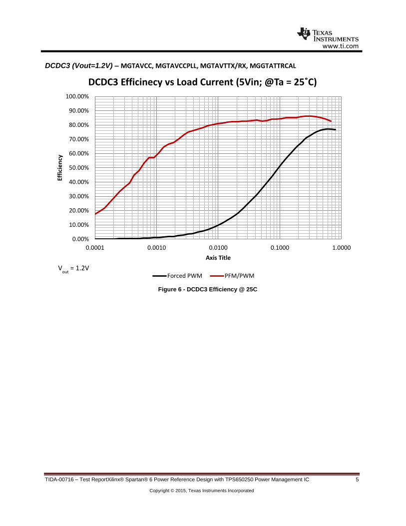
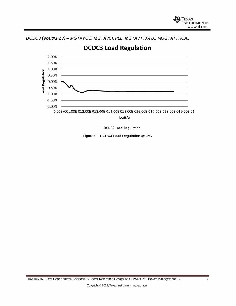
DCDC3 (Vout=1.2V) – MGTAVCC, MGTAVCCPLL, MGTAVTTX/RX, MGGTATTRCAL
Figure 6 - DCDC3 Efficiency @ 25C
0.00%
10.00%
20.00%
30.00%
40.00%
50.00%
60.00%
70.00%
80.00%
90.00%
100.00%
0.0001 0.0010 0.0100 0.1000 1.0000
Effi
cie
ncy
Axis Title
DCDC3 Efficinecy vs Load Current (5Vin; @Ta = 25˚C)
Forced PWM PFM/PWMV
out = 1.2V
www.ti.com
TIDA-00716 – Test ReportXilinx® Spartan® 6 Power Reference Design with TPS650250 Power Management IC 6
Copyright © 2015, Texas Instruments Incorporated
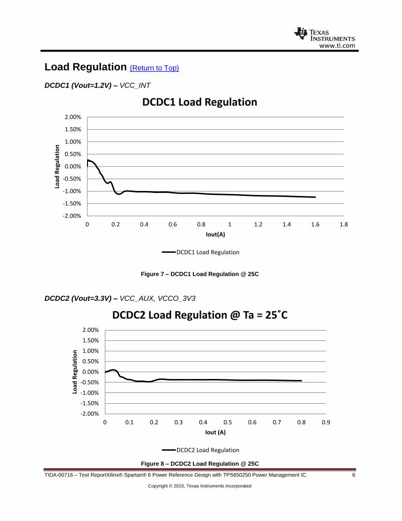
Load Regulation (Return to Top)
DCDC1 (Vout=1.2V) – VCC_INT
Figure 7 – DCDC1 Load Regulation @ 25C
DCDC2 (Vout=3.3V) – VCC_AUX, VCCO_3V3
Figure 8 – DCDC2 Load Regulation @ 25C
-2.00%
-1.50%
-1.00%
-0.50%
0.00%
0.50%
1.00%
1.50%
2.00%
0 0.2 0.4 0.6 0.8 1 1.2 1.4 1.6 1.8
Load
Re
gula
tio
n
Iout(A)
DCDC1 Load Regulation
DCDC1 Load Regulation
-2.00%
-1.50%
-1.00%
-0.50%
0.00%
0.50%
1.00%
1.50%
2.00%
0 0.1 0.2 0.3 0.4 0.5 0.6 0.7 0.8 0.9
Load
Re
gula
tio
n
Iout (A)
DCDC2 Load Regulation @ Ta = 25˚C
DCDC2 Load Regulation
www.ti.com
TIDA-00716 – Test ReportXilinx® Spartan® 6 Power Reference Design with TPS650250 Power Management IC 7
Copyright © 2015, Texas Instruments Incorporated
DCDC3 (Vout=1.2V) – MGTAVCC, MGTAVCCPLL, MGTAVTTX/RX, MGGTATTRCAL
Figure 9 – DCDC3 Load Regulation @ 25C
-2.00%
-1.50%
-1.00%
-0.50%
0.00%
0.50%
1.00%
1.50%
2.00%
0.00E+001.00E-012.00E-013.00E-014.00E-015.00E-016.00E-017.00E-018.00E-019.00E-01
Load
Re
gula
tio
n
Iout(A)
DCDC3 Load Regulation
DCDC2 Load Regulation
www.ti.com
TIDA-00716 – Test ReportXilinx® Spartan® 6 Power Reference Design with TPS650250 Power Management IC 8
Copyright © 2015, Texas Instruments Incorporated
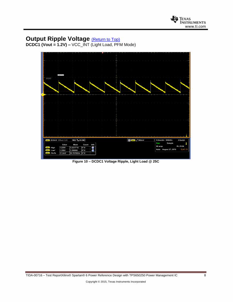
Output Ripple Voltage (Return to Top)
DCDC1 (Vout = 1.2V) – VCC_INT (Light Load, PFM Mode)
Figure 10 – DCDC1 Voltage Ripple, Light Load @ 25C
www.ti.com
TIDA-00716 – Test ReportXilinx® Spartan® 6 Power Reference Design with TPS650250 Power Management IC 9
Copyright © 2015, Texas Instruments Incorporated
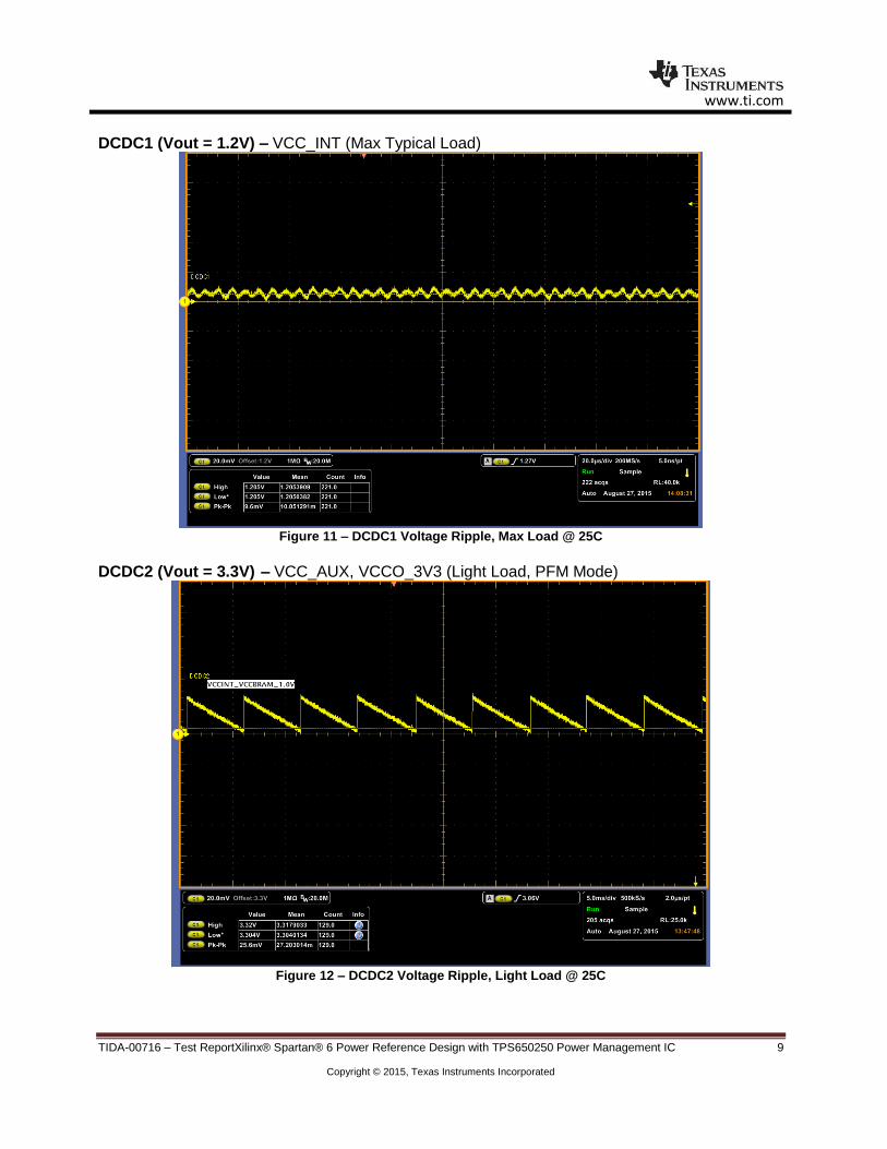
DCDC1 (Vout = 1.2V) – VCC_INT (Max Typical Load)
Figure 11 – DCDC1 Voltage Ripple, Max Load @ 25C
DCDC2 (Vout = 3.3V) – VCC_AUX, VCCO_3V3 (Light Load, PFM Mode)
Figure 12 – DCDC2 Voltage Ripple, Light Load @ 25C
www.ti.com
TIDA-00716 – Test ReportXilinx® Spartan® 6 Power Reference Design with TPS650250 Power Management IC 10
Copyright © 2015, Texas Instruments Incorporated
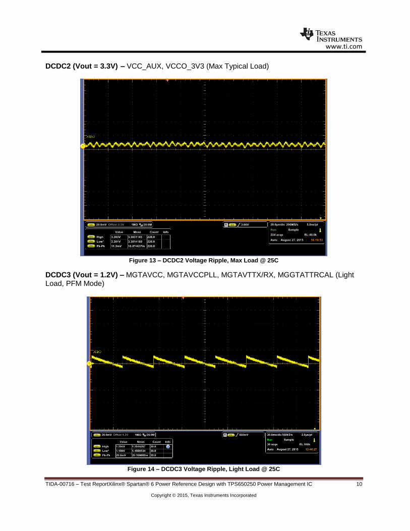
DCDC2 (Vout = 3.3V) – VCC_AUX, VCCO_3V3 (Max Typical Load)
Figure 13 – DCDC2 Voltage Ripple, Max Load @ 25C
DCDC3 (Vout = 1.2V) – MGTAVCC, MGTAVCCPLL, MGTAVTTX/RX, MGGTATTRCAL (Light Load, PFM Mode)
Figure 14 – DCDC3 Voltage Ripple, Light Load @ 25C
www.ti.com
TIDA-00716 – Test ReportXilinx® Spartan® 6 Power Reference Design with TPS650250 Power Management IC 11
Copyright © 2015, Texas Instruments Incorporated
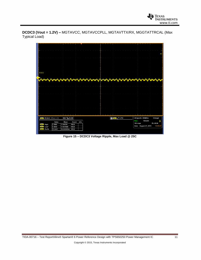
DCDC3 (Vout = 1.2V) – MGTAVCC, MGTAVCCPLL, MGTAVTTX/RX, MGGTATTRCAL (Max Typical Load)
Figure 15 – DCDC3 Voltage Ripple, Max Load @ 25C
www.ti.com
TIDA-00716 – Test ReportXilinx® Spartan® 6 Power Reference Design with TPS650250 Power Management IC 12
Copyright © 2015, Texas Instruments Incorporated
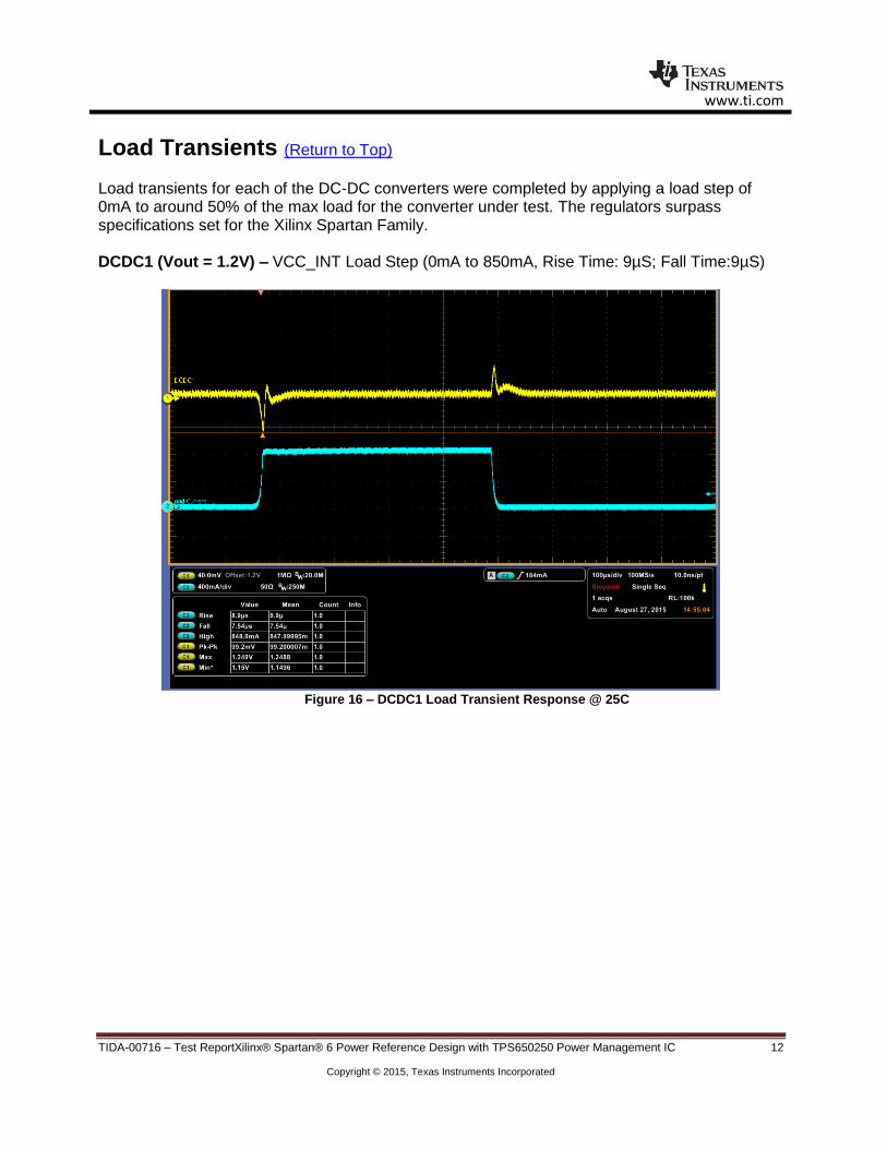
Load Transients (Return to Top)
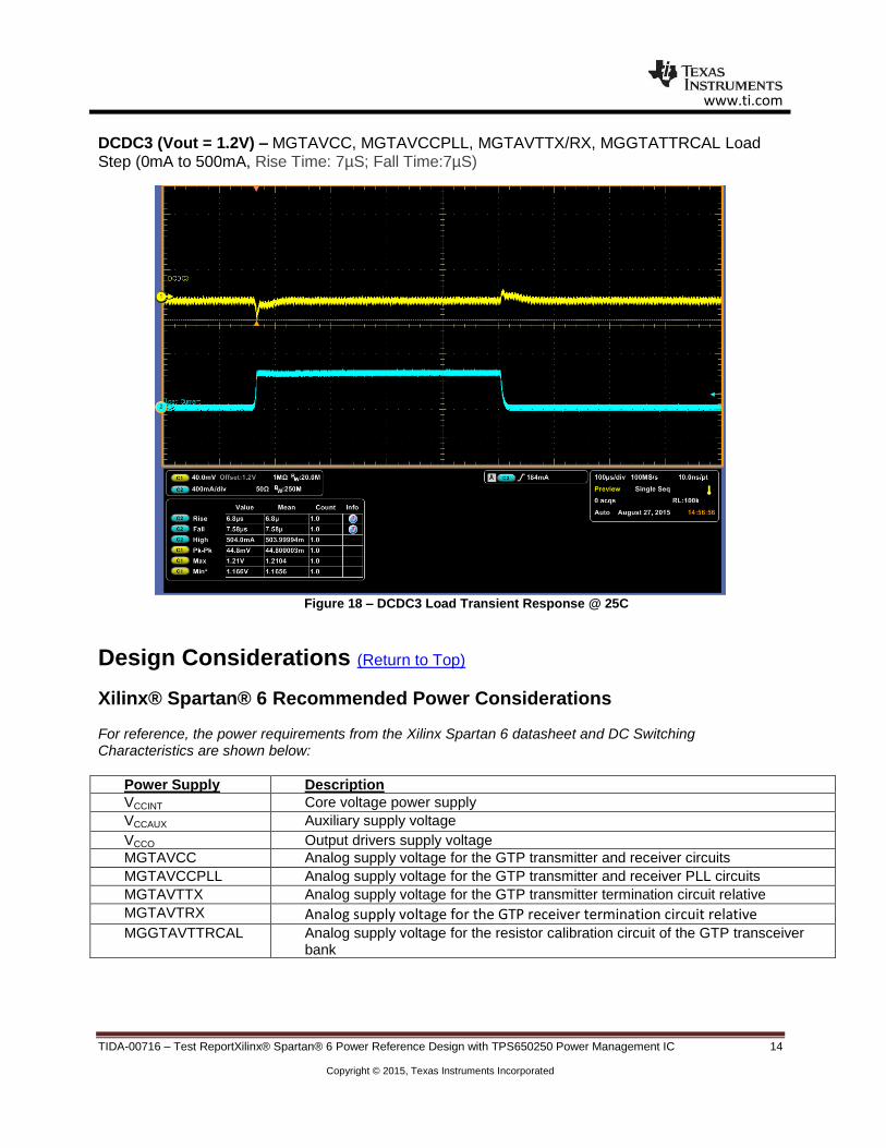
Load transients for each of the DC-DC converters were completed by applying a load step of 0mA to around 50% of the max load for the converter under test. The regulators surpass specifications set for the Xilinx Spartan Family. DCDC1 (Vout = 1.2V) – VCC_INT Load Step (0mA to 850mA, Rise Time: 9µS; Fall Time:9µS)
Figure 16 – DCDC1 Load Transient Response @ 25C
www.ti.com
TIDA-00716 – Test ReportXilinx® Spartan® 6 Power Reference Design with TPS650250 Power Management IC 13
Copyright © 2015, Texas Instruments Incorporated
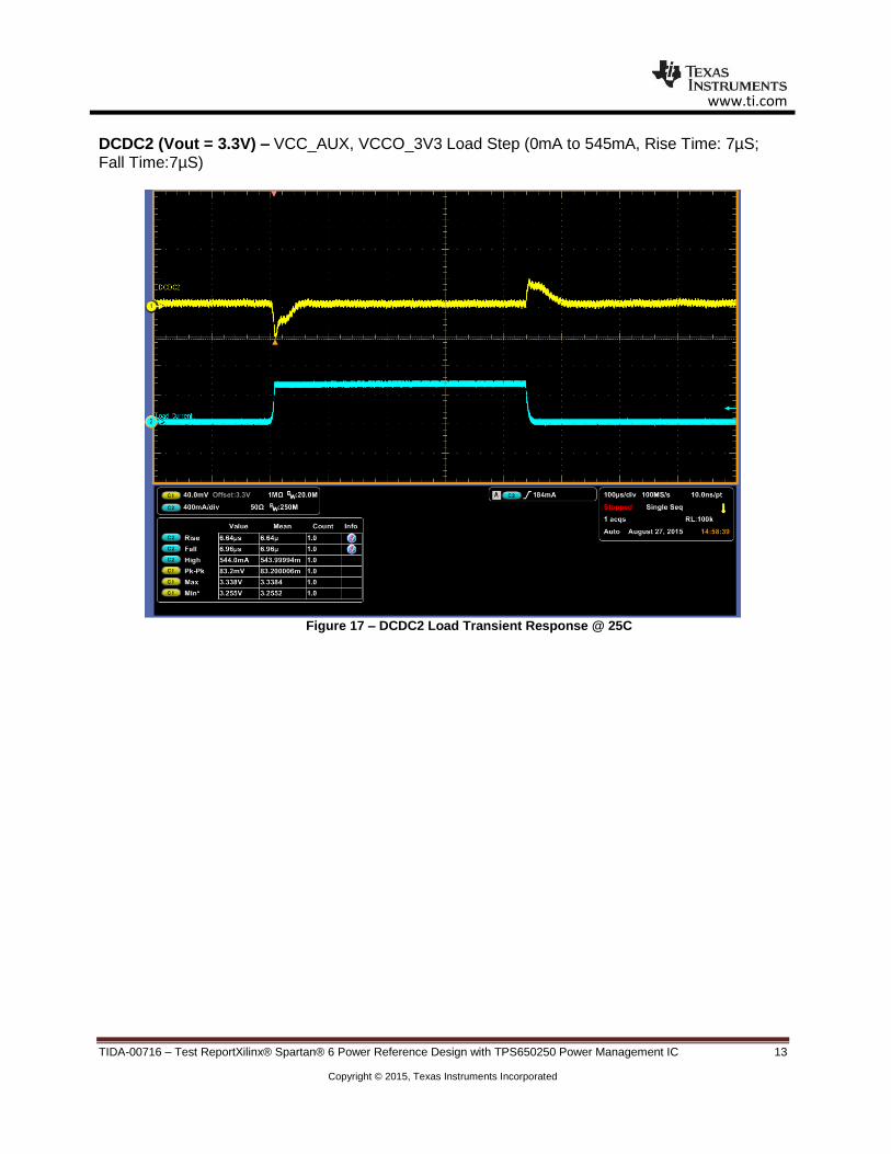
DCDC2 (Vout = 3.3V) – VCC_AUX, VCCO_3V3 Load Step (0mA to 545mA, Rise Time: 7µS; Fall Time:7µS)
Figure 17 – DCDC2 Load Transient Response @ 25C
www.ti.com
TIDA-00716 – Test ReportXilinx® Spartan® 6 Power Reference Design with TPS650250 Power Management IC 14
Copyright © 2015, Texas Instruments Incorporated
DCDC3 (Vout = 1.2V) – MGTAVCC, MGTAVCCPLL, MGTAVTTX/RX, MGGTATTRCAL Load Step (0mA to 500mA, Rise Time: 7µS; Fall Time:7µS)
Figure 18 – DCDC3 Load Transient Response @ 25C
Design Considerations (Return to Top)
Xilinx® Spartan® 6 Recommended Power Considerations For reference, the power requirements from the Xilinx Spartan 6 datasheet and DC Switching Characteristics are shown below:
Power Supply Description
VCCINT Core voltage power supply
VCCAUX Auxiliary supply voltage
VCCO Output drivers supply voltage
MGTAVCC Analog supply voltage for the GTP transmitter and receiver circuits
MGTAVCCPLL Analog supply voltage for the GTP transmitter and receiver PLL circuits
MGTAVTTX Analog supply voltage for the GTP transmitter termination circuit relative
MGTAVTRX Analog supply voltage for the GTP receiver termination circuit relative
MGGTAVTTRCAL Analog supply voltage for the resistor calibration circuit of the GTP transceiver bank
www.ti.com
TIDA-00716 – Test ReportXilinx® Spartan® 6 Power Reference Design with TPS650250 Power Management IC 15
Copyright © 2015, Texas Instruments Incorporated
Power Sequencing Requirements The Spartan 6 can be powered up and powered down in any sequence. In order for the POR Circuit to be released, all the inputs need to be valid, thus there is no specific order the rails must come up. Refer to the Spartan 6 Users Guide: (http://www.xilinx.com/support/documentation/user_guides/ug380.pdf) for Power-On Sequence Precautions when using other device in the system such as SPI Flash. Power Supply Ramp Time:
Power Supply Ramp Time
VCCINT 0.20 to 50.0ms
VCCAUX 0.20 to 50.0ms
VCCO 0.20 to 50.0ms
TPS650250 Recommended Power Considerations
Input Voltage Filter An RC filter connected at the Vcc input is used to keep noise from the internal supply for the bandgap and other analog circuitry. A typical value of 1 Ω and 1 μF is used to filter the switching spikes, generated by the DC-DC converters. A larger resistor than 10 Ω should not be used because the current into Vcc of up to 2.5 mA causes a voltage drop at the resistor causing the undervoltage lockout circuitry connected at Vcc internally to switch off too early. Input Capacitor Selection Because of the nature of the buck converter having a pulsating input current, a low ESR input capacitor is required for best input voltage filtering and minimizing interference with other circuits caused by high input voltage spikes. Each DC-DC converter requires a 10 µF ceramic input capacitor on its input pin VINDCDCx. The input capacitor can be increased without any limit for better input voltage filtering. The Vcc pin should be separated from the input for the DC-DC converters. A filter resistor of up to 10 Ω and a 1 μF capacitor should be used for decoupling the Vcc pin from switching noise. Note that the filter resistor may affect the UVLO threshold since up to 3 mA can flow via this resistor into the Vcc pin when all converters are running in PWM mode.
CAPACITOR VALUE
CASE SIZE COMPONENT SUPPLIER COMMENTS
22µF 1206 TDK C3216X5R0J226M Ceramic
22µF 1206 Taiyo Yuden JMK316BJ226ML Ceramic
22µF 0805 TDK C2012X5R0J226MT Ceramic
22µF 0805 Taiyo Yuden JMK212BJ226MG Ceramic
10µF 0805 Taiyo Yuden JMK212BJ106M Ceramic
10µF 0805 TDK C2012X5R0J106M Ceramic
www.ti.com
TIDA-00716 – Test ReportXilinx® Spartan® 6 Power Reference Design with TPS650250 Power Management IC 16
Copyright © 2015, Texas Instruments Incorporated
Power Supply Recommendations The TPS650250 is designed to operate from an input voltage supply range between 3.5 V and 5.5 V. The input supply should be well regulated. If the input supply is located more than a few inches from the TPS650250, additional bulk capacitance may be required in addition to the ceramic bypass capacitors. Output Voltage Selection: The DCDC Converters can be set via an external resistor divider or by the logic level of the DEDCDCX pins.
If the desired voltages cannot be met, using an external resistor divider will allow the user to select a voltage between 0.6V up to the input.
The output voltage of the LDO1 and LDO2 are set via an external resistor divider. VFBLDOX = 1.0V
Inductor Selection for Buck Converters: The three converters operate with 2.2 µH output inductors. Larger or smaller inductor values can be used to optimize performance of the device for specific conditions. The selected inductor has to be rated for its DC resistance and saturation current. The DC resistance of the inductor influences directly the efficiency of the converter. Therefore, an inductor with the lowest DC resistance should be selected for the highest efficiency. For a fast transient response, a 2.2 μH inductor in combination with a 22 μF output capacitor is recommended. For an output voltage above 2.8 V, an inductor value of 3.3 μH minimum is required. Lower values result in an increased output voltage ripple in PFM mode. The minimum inductor value is 1.5 μH, but an output capacitor of 22 μF minimum is needed in this case.
www.ti.com
TIDA-00716 – Test ReportXilinx® Spartan® 6 Power Reference Design with TPS650250 Power Management IC 17
Copyright © 2015, Texas Instruments Incorporated
The equation below calculates the maximum inductor current under static load conditions. The saturation current of the inductor should be rated higher than the maximum inductor current as calculated with Equation 4. This is recommended because during heavy load transient the inductor current rises above the calculated value.
Open core inductors have a soft saturation characteristic and they can usually handle higher inductor currents versus a comparable shielded inductor. A more conservative approach is to select the inductor current rating just for the maximum switch current of the corresponding converter. Consideration must be given to the difference in the core material from inductor to inductor which has an impact on efficiency especially at high switching frequencies. Layout Guidelines
The VINDCDC1, VINDCDC2 and VINDCDC3 terminals should be bypassed to ground with a low ESR ceramic bypass capacitor. The typical recommended bypass capacitance is 10 uF ceramic with a X5R or X7R dielectric.
The VINLDO terminal should be bypassed to ground with a low ESR ceramic bypass capacitor. The typical recommended bypass capacitance is 1 uF ceramic with a X5R or X7R dielectric.
The optimum placement is closest to the individual voltage terminals and the AGNDx terminals
The AGNDx terminals should be tied to the PCB ground plane at the terminal of the IC.
The cross sectional area loop from the input capacitor to the VINDCDCx input and corresponding PGNDx terminal should be minimized as much as possible.
Route the feedback signal for each of the step-down converters next to the current path of the converter in order to decrease the cross sectional area of the feedback loop which minimizes noise injection into the loop.
Do not route any noise sensitive signals under or next to any of the step-down inductors. Ensure a keepout region directly under the inductors or at least provide ground shielding.
It is recommended to have the layer directly underneath the IC to be a solid copper ground plane.
www.ti.com
TIDA-00716 – Test ReportXilinx® Spartan® 6 Power Reference Design with TPS650250 Power Management IC 18
Copyright © 2015, Texas Instruments Incorporated
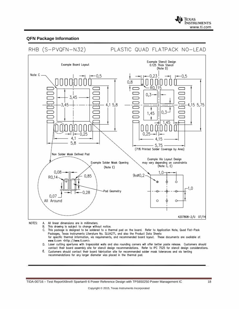
QFN Package Information
www.ti.com
TIDA-00716 - Test ReportXilinx® Spartan® 6 Power Reference Design with TPS650250 Power Management IC 19
Copyright © 2015, Texas Instruments Incorporated
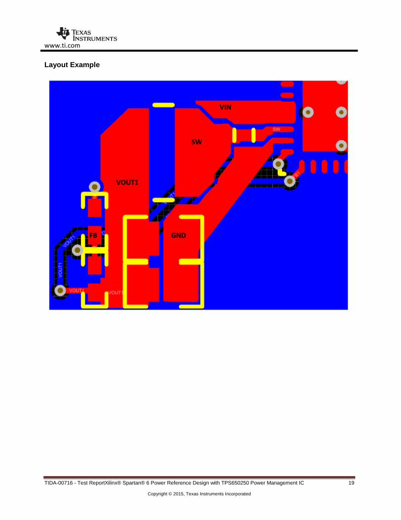
Layout Example
IMPORTANT NOTICE FOR TI REFERENCE DESIGNS
Texas Instruments Incorporated ("TI") reference designs are solely intended to assist designers (“Buyers”) who are developing systems thatincorporate TI semiconductor products (also referred to herein as “components”). Buyer understands and agrees that Buyer remainsresponsible for using its independent analysis, evaluation and judgment in designing Buyer’s systems and products.TI reference designs have been created using standard laboratory conditions and engineering practices. TI has not conducted anytesting other than that specifically described in the published documentation for a particular reference design. TI may makecorrections, enhancements, improvements and other changes to its reference designs.Buyers are authorized to use TI reference designs with the TI component(s) identified in each particular reference design and to modify thereference design in the development of their end products. HOWEVER, NO OTHER LICENSE, EXPRESS OR IMPLIED, BY ESTOPPELOR OTHERWISE TO ANY OTHER TI INTELLECTUAL PROPERTY RIGHT, AND NO LICENSE TO ANY THIRD PARTY TECHNOLOGYOR INTELLECTUAL PROPERTY RIGHT, IS GRANTED HEREIN, including but not limited to any patent right, copyright, mask work right,or other intellectual property right relating to any combination, machine, or process in which TI components or services are used.Information published by TI regarding third-party products or services does not constitute a license to use such products or services, or awarranty or endorsement thereof. Use of such information may require a license from a third party under the patents or other intellectualproperty of the third party, or a license from TI under the patents or other intellectual property of TI.TI REFERENCE DESIGNS ARE PROVIDED "AS IS". TI MAKES NO WARRANTIES OR REPRESENTATIONS WITH REGARD TO THEREFERENCE DESIGNS OR USE OF THE REFERENCE DESIGNS, EXPRESS, IMPLIED OR STATUTORY, INCLUDING ACCURACY ORCOMPLETENESS. TI DISCLAIMS ANY WARRANTY OF TITLE AND ANY IMPLIED WARRANTIES OF MERCHANTABILITY, FITNESSFOR A PARTICULAR PURPOSE, QUIET ENJOYMENT, QUIET POSSESSION, AND NON-INFRINGEMENT OF ANY THIRD PARTYINTELLECTUAL PROPERTY RIGHTS WITH REGARD TO TI REFERENCE DESIGNS OR USE THEREOF. TI SHALL NOT BE LIABLEFOR AND SHALL NOT DEFEND OR INDEMNIFY BUYERS AGAINST ANY THIRD PARTY INFRINGEMENT CLAIM THAT RELATES TOOR IS BASED ON A COMBINATION OF COMPONENTS PROVIDED IN A TI REFERENCE DESIGN. IN NO EVENT SHALL TI BELIABLE FOR ANY ACTUAL, SPECIAL, INCIDENTAL, CONSEQUENTIAL OR INDIRECT DAMAGES, HOWEVER CAUSED, ON ANYTHEORY OF LIABILITY AND WHETHER OR NOT TI HAS BEEN ADVISED OF THE POSSIBILITY OF SUCH DAMAGES, ARISING INANY WAY OUT OF TI REFERENCE DESIGNS OR BUYER’S USE OF TI REFERENCE DESIGNS.TI reserves the right to make corrections, enhancements, improvements and other changes to its semiconductor products and services perJESD46, latest issue, and to discontinue any product or service per JESD48, latest issue. Buyers should obtain the latest relevantinformation before placing orders and should verify that such information is current and complete. All semiconductor products are soldsubject to TI’s terms and conditions of sale supplied at the time of order acknowledgment.TI warrants performance of its components to the specifications applicable at the time of sale, in accordance with the warranty in TI’s termsand conditions of sale of semiconductor products. Testing and other quality control techniques for TI components are used to the extent TIdeems necessary to support this warranty. Except where mandated by applicable law, testing of all parameters of each component is notnecessarily performed.TI assumes no liability for applications assistance or the design of Buyers’ products. Buyers are responsible for their products andapplications using TI components. To minimize the risks associated with Buyers’ products and applications, Buyers should provideadequate design and operating safeguards.Reproduction of significant portions of TI information in TI data books, data sheets or reference designs is permissible only if reproduction iswithout alteration and is accompanied by all associated warranties, conditions, limitations, and notices. TI is not responsible or liable forsuch altered documentation. Information of third parties may be subject to additional restrictions.Buyer acknowledges and agrees that it is solely responsible for compliance with all legal, regulatory and safety-related requirementsconcerning its products, and any use of TI components in its applications, notwithstanding any applications-related information or supportthat may be provided by TI. Buyer represents and agrees that it has all the necessary expertise to create and implement safeguards thatanticipate dangerous failures, monitor failures and their consequences, lessen the likelihood of dangerous failures and take appropriateremedial actions. Buyer will fully indemnify TI and its representatives against any damages arising out of the use of any TI components inBuyer’s safety-critical applications.In some cases, TI components may be promoted specifically to facilitate safety-related applications. With such components, TI’s goal is tohelp enable customers to design and create their own end-product solutions that meet applicable functional safety standards andrequirements. Nonetheless, such components are subject to these terms.No TI components are authorized for use in FDA Class III (or similar life-critical medical equipment) unless authorized officers of the partieshave executed an agreement specifically governing such use.Only those TI components that TI has specifically designated as military grade or “enhanced plastic” are designed and intended for use inmilitary/aerospace applications or environments. Buyer acknowledges and agrees that any military or aerospace use of TI components thathave not been so designated is solely at Buyer's risk, and Buyer is solely responsible for compliance with all legal and regulatoryrequirements in connection with such use.TI has specifically designated certain components as meeting ISO/TS16949 requirements, mainly for automotive use. In any case of use ofnon-designated products, TI will not be responsible for any failure to meet ISO/TS16949.IMPORTANT NOTICE
Mailing Address: Texas Instruments, Post Office Box 655303, Dallas, Texas 75265Copyright © 2015, Texas Instruments Incorporated