Embed Size (px)
Citation preview
CHAPTER 11
XlLlNX SPARTAN-3 SPECIFIC MEMORY
11.1 INTRODUCTION
A digital system frequently requires memory for storage. To facilitate this need, most FPGA devices contain dedicated embedded memory modules. While these modules cannot replace the massive external memory devices, they are useful for applications that require small or intermediate-sized memory.
Although the basic internal structure of memory modules is similar, there are many subtle differences in their I/O interfaces. It is usually difficult for synthesis software to extract the desired features from the code and to infer a matching memory module from the underlying device library. In Xilinx ISE, we can use HDL instantiation, the Core Generator program, or the behavioral HDL inference template to incorporate an embedded memory module into a design. The third one is semi-device independent and we use this method in this book. In this chapter, we briefly examine Spartan-3 memory modules and the first two methods and provide detailed descriptions of several key behavioral HDL templates.
11.2 EMBEDDED MEMORY OF SPARTAN-3 DEVICE
11.2.1 Overview
There are two types of embedded memory in a Spartan-3 device: distributed RAM and block RAM. A distributed RAM is constructed from the logic cell’s look-up table (LUT). The LUT can be configured as a 16-by-1 synchronous RAM, and multiple LUTs can be
FPGA Prototyping by VHDL Examples. B y Pong P. Chu Copyright @ 2008 John Wiley & Sons, Inc.
243
244 XlLlNX SPARTAN-3 SPECIFIC MEMORY
cascaded to form a wider and deeper memory module. The Spartan-3 XC3S200 device of the S3 board can provide up to 30K bits of distributed memory, which is small compared to a block RAM or external memory. Furthermore, since the distributed RAM uses the logic cells, it competes for resources with the normal logic. Thus, it is feasible only for applications that require relatively small storage.
A block RAM is a special memory module embedded in an FPGA device and is separated from the regular logic cells. It can be thought of as a fast SRAM wrapped by a synchronous, configurable interface. Each block RAM consists of 16K (214) data bits plus optional 2K parity bits. It can be organized in different widths, from 16K by 1 (i.e., 214 by 2’) to 512 by 32 (i.e., 2’ by 25). The Spartan-3 XC3S200 device has 12 block RAMs, totaling 172K data bits. These block RAMs can be used for intermediate-sized applications, such as a FIFO, a large look-up table, or an intermediate-sized local memory. In comparison, the external SRAM chips of the S3 board have a capacity of 8M bits.
Both the distributed RAM and block RAM are already “wrapped” with a synchronous interface, and thus no additional memory controller circuit is needed. They are very flexible and can be configured to perform single- and dual-port access and to support various types of buffering and clocking schemes. Detailed discussion is beyond the scope of this book. We only examine several commonly used configurations, including a synchronous single-port RAM, a synchronous dual-port RAM, and a ROM in Section 11.4.
11.2.2 Comparison
The Spartan-3 device and the S3 board provide several options for storage elements. It is a good idea to keep in mind the relative capacities of these options:
0 XC3S2OO’s FFs (for registers): about 4.5K bits, embedded in logic cells and IiO
0 XC3S2OO’s distributed RAM: 30K bits, constructed from the logic cells 0 XC3S2OO’s block RAM: 172K bits, configured as twelve 16K-bit modules 0 External SRAM: 8M bits, configured as two 256K-by-16 SRAM chips
This helps us to decide which option is most suitable for an application at hand.
buffers
11.3 METHOD TO INCORPORATE MEMORY MODULES
Although memory modules have similar internal structure, there are many subtle differences in their interfaces, such as the numbers of read and write ports, clocking scheme, data and address buffering, enable and reset signals, and initial values. Although it is possible to describe the desired module behaviors in HDL code, the synthesis software may or may not recognize the designer’s intention. Therefore, the HDL code cannot always infer the proper memory module and is normally not portable. In Xilinx ISE, there are three methods to incorporate an embedded memory module into a design:
0 HDL instantiation 0 The Core Generator program 0 The behavioral HDL inference template
The first two are specific for Xilinx devices and the third is a semi-device-independent behavioral description. Because of the clarity of the behavioral description, we use the third method in this book. We provide a brief overview of the three methods in this section.
METHOD TO INCORPORATE MEMORY MODULES 245
11.3.1
We have used HDL component instantiation in many earlier design examples to include predesigned modules or to create a hierarchy, Instantiating a Xilinx memory module is similar except that there is no HDL description for the architecture body. We must check the manual to find the exact entity name and the associated generics and I/O port definitions. This is a tedious process and is particularly error-prone for memory modules because of the large number of configurations and options.
The instantiation code for many Xilinx components can be obtained directly from ISE by selecting Edit + Language Templates. The following are segments of a 16K-by-1 dual-port RAM:
Memory module via HDL component instantiation
-- R A M B 1 6 - S L S I : V i r t e x - I I / I I - P r o , -- S p a r t a n -3/3E 1 6 k x 1 D u a l - P o r t RAM __ X i l i n x HDL L a n g u a g e T e m p l a t e v e r s i o n 8 . 1 i RAMB16-S1-Sl-inst : RAMBlG-Sl-Sl g e n e r i c map(
init-a => "0" , init-b => "0" , srval-a = > "0" , srval-b = > "0" , write-mode-a = > "WRITE-FIRST", write-mode-b = > "WRITE-FIRST" , s im- c o 11 i s i on- c he c k = > " ALL ' I , init-00 = > x"0 . . . 0",
init-3f = > x"0 . . . 0" . . .
I ,
p o r t map( doa = > doa, dob = > dob, addra => addra, addrb = > addrb , clka => clka, clkb => clkb, dia => dia, dib = > dib, ena = > ena, enb = > enb , ssra => s s r a , ssrb = > ssrb, wea = > wea, web = > web
) ;
__ p o r t __ p o r t __ p o r t __ p o r t __ p o r t
p o r t __ p o r t __ p o r t _- p o r t __ p o r t -_ p o r t __ p o r t __ p o r t __ p o r t
__
a I - b i t d a t a o u t p u t b 1 - b i t d a t a o u t p u t a 1 4 - b i t a d d r e s s i n p u t b 1 4 - b i t a d d r e s s i n p u t a c l o c k b c l o c k a 1 - b i t d a t a i n p u t b 1 - b i t d a t a i n p u t a ram e n a b l e i n p u t b ram e n a b l e i n p u t a s y n c h r o n o u s s e t / r e s e t i n p u t b s y n c h r o n o u s s e t / r e s e t i n p u t a w r i t e e n a b l e i n p u t b w r i t e e n a b l e i n p u t
Although the code is readily available, we must study the manual carefully to find the right component and proper configuration parameters.
11.3.2 Memory module via Core Generator
To simplify the instantiation process, Xilinx provides a utility program, known as Core Generator (Coregen), to generate Xilinx-specific components. This utility can be invoked from the ISE environment by selecting Project + New Source. After the New Source
246 XlLlNX SPARTAN-3 SPECIFIC MEMORY
Wizard dialog appears, we select IP (Coregen & Architecture Wizard) to invoke the Coregen program. The program guides the users through a series of questions and then generates several files. The file with the .xco extension is a text file that contains the information necessary to construct the desired memory component. The file with the .vhd extension contains the “wrapper” code for simulation purpose. This file cannot be used to instantiate the desired component and is ignored during the synthesis process.
Although using the Coregen program is more convenient than direct HDL instantiation, it is not within the HDL framework and can lead to a compatibility problem when a design is not done in the Xilinx ISE environment.
11.3.3 Memory module via HDL inference
Although it is not possible to develop a device-independent HDL description, the synthe- sis program of ISE, known as XST, provides a collection of behavioral HDL templates to infer memory modules from Xilinx FPGA devices. These templates are done by behav- ioral descriptions and contain no device-specific component instantiation. They are easy to understand and can be simulated without an additional HDL library. However, while the de- scription does not explicitly refer to any Xilinx component, the code may not be recognized by other third-party synthesis software, and the desired memory module cannot always be inferred. Thus, these templates can best be described as “semi-portable” and “semi-device- independent” behavioral descriptions. Templates for commonly used memory modules are discussed in Section 1 1.4.
On the downside, the template approach is based on the ability of the XST software to recognize the template and infer the proper memory module accordingly. The software may change during upgrade or misinterpret some code. It is a good idea to check the XST synthesis report to ensure that the desired memory module is inferred correctly.
11.4 HDL TEMPLATES FOR MEMORY INFERENCE
To use behavioral HDL description to infer the Xilinx memory module, the XST’s templates should be followed closely. To avoid misinterpretation, we should refrain from creating our own “innovative” code. The codes in the following subsections are all based on templates of the XST v8.1 i Manual. They are the same as the original templates except that generics are used for the width of address bits and the width of data bits, and the numeric-std package is used to replace the proprietary std-logic-unsigned package. It is a good practice to confine the memory description in a separate HDL module so that the module can easily be identified and replaced when needed. In this section, we discuss the behavioral HDL templates for six configurations, including two for single-port RAMs, two for dual-port RAMs, and two for ROMs.
11.4.1 Single-port RAM
The embedded memory of a Spartan-3 device is already wrapped with a synchronous interface similar to that in Section 10.3. Its write operation is always synchronous. At the rising edge of the clock, the address, input data, and relevant control signals, such as we (i.e., write enable), are sampled. If we is asserted, a write operation is performed (i.e., the input data is stored into the memory location designated by the address signal).
HDL TEMPLATES FOR MEMORY INFERENCE 247
The read operation can be asynchronous or synchronous. For asynchronous read, the address signal is used directly to access the RAM array. After the address signal changes, the data becomes available after a short delay. For synchronous read, the address signal is sampled at the rising edge of the clock and stored in a register. The registered address is then used to access the RAM array. Because of the register, the availability of data is delayed and is synchronized by the clock signal. Due to the internal structure, asynchronous read operation can only be realized by the distributed RAM.
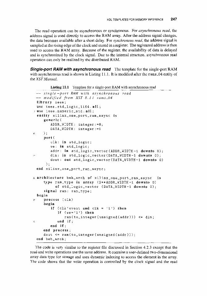
Single-port RAM with asynchronous read The template for the single-port RAM with asynchronous read is shown in Listing 11.1. It is modified after the rams-04 entity of the XST Manual.
Listing 11.1 Template for a single-port RAM with asynchronous read
__ single - p o r t RAM w i t h a s y n c h r o n o u s read __ m o d i f i e d f r o m XST 8 . 1 i rams-04 l i b r a r y ieee; use ieee. std-logic-1164. a l l ;
e n t i t y xilinx-one-port-ram-async i s 5 use ieee. numeric-std. a l l ;
g e n e r i c ( ADDR-WIDTH : DATA-WIDTH : integer : =1
integer : =8 ;
10 ) ; p o r t (
c l k : in std-logic; we: i n std-logic; addr : i n std-logic-vector (ADDR-WIDTH-1 downto 0) ;
dout : o u t std-logic-vector (DATA-WIDTH-1 downto 0) I 5 din: i n std-logic-vector (DATA-WIDTH -1 downto 0 ) ;
) ; end xilinx-one-port-ram-async;
i0
20 a r c h i t e c t u r e be h - ar c h of x i 1 i nx - one - p or t - r am - as y n c i s t y p e ram-type i s a r r a y (2**ADDR_WIDTH -1 downto 0 )
of std-logic-vector (DATA-WIDTH-1 downto 0 ) ; s i g n a l ram: ram-type;
b e g i n z i p r o c e s s (clk)
b e g i n i f (clk’event and clk = ’1’) then
i f (we=’l’) t h e n
end i f ; ram(to-integer (unsigned(addr1)) <= din;
end i f ; end p r o c e s s ; dout <= ram(to-integer(unsigned(addr)));
end beh-arch ;
The code is very similar to the register file discussed in Section 4.2.3 except that the read and write operations use the same address. It contains a user-defined two-dimensional array data type for storage and uses dynamic indexing to access the element in the array. The code shows that the write operation is controlled by the clock signal and the read
248 XlLlNX SPARTAN-3 SPECIFIC MEMORY
operation depends only on the address. Since asynchronous read can be realized only by the distributed RAM, this configuration is only recommended for applications that require small storage.
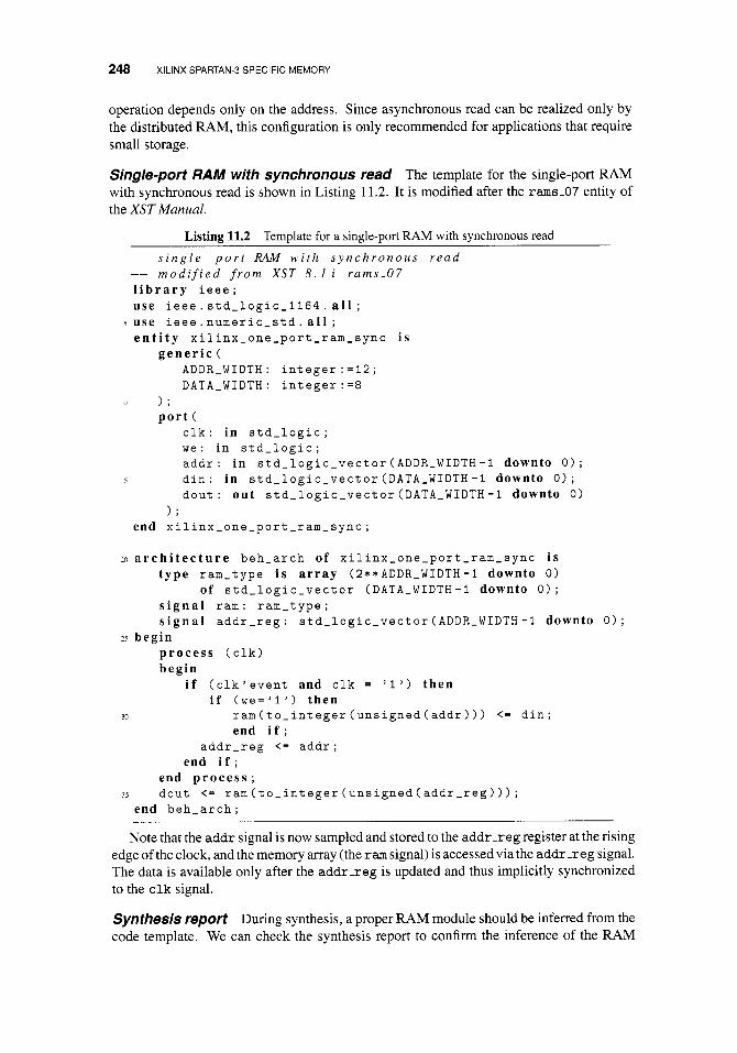
Single-port RAM with synchronous read The template for the single-port RAM with synchronous read is shown in Listing 11.2. It is modified after the rams-07 entity of the XST Manual.
Listing 11.2 Template for a single-port RAM with synchronous read
__ s i n g l e - p o r t RAM w i t h s y n c h r o n o u s r e a d __ m o d i f i e d f r o m X S T 8 . 1 i r a m s - 0 7 l i b r a r y ieee; use ieee. std-logic-1164. a l l ;
s use ieee. numeric-std. a l l ; e n t i t y xilinx-one-port -ram-sync i s
g e n e r i c ( ADDR-WIDTH : DATA-WIDTH : integer : =8
integer : =12 ;
10 ) ; port (
clk: in std-logic; w e : in std-logic; addr: in std-logic-vector (ADDR-WIDTH-1 downto 0 ) ;
dout : out std-logic-vector (DATA-WIDTH -1 downto 0 ) IS d i n: in std-logic-vector (DATA-WIDTH-1 downto 0) ;
1 ; end xilinx-one-port-ram-sync;
20 a r c h i t e c t u r e be h - ar c h of x i 1 i nx - one -port - r am - s y n c i s type ram-type i s array (2**ADDR_WIDTH -1 downto 0 )
of std-logic-vector (DATA-WIDTH-1 downto 0 ) ; s i g n a l ram: ram-type; s i g n a l addr-reg: std-logic-vector (ADDR-WIDTH-1 downto 0 ) ;
p r o c e s s (clk) beg in
25 beg in
i f (clk’event and clk = ’ 1 ’ ) then i f ( w e = ’ l ’ ) then
30 ram(to-integer(unsigned(addr))) <= d i n ; end i f ;
addr-reg <= addr; end i f ;
end p r o c e s s ; 35 dout <= ram(to-integer (unsigned(addr-reg))) ;
end beh-arch ;
Note that the addr signal is now sampled and stored to the addr-reg register at the rising edge of the clock, and the memory array (the ram signal) is accessed via the addr-reg signal. The data is available only after the addr-reg is updated and thus implicitly synchronized to the clk signal.
Synthesis report During synthesis, a proper RAM module should be inferred from the code template. We can check the synthesis report to confirm the inference of the RAM
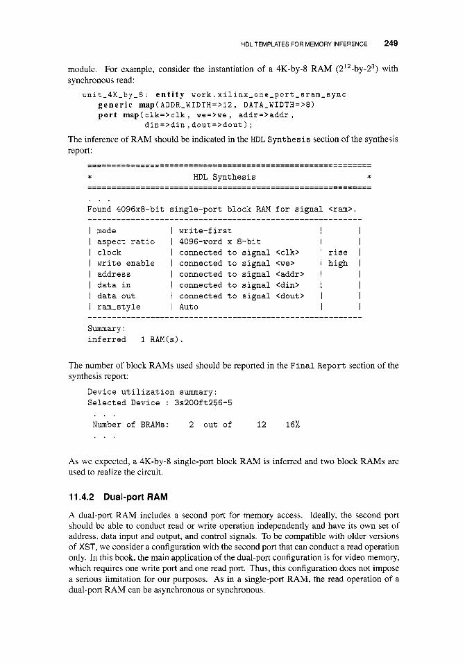
HDL TEMPLATES FOR MEMORY INFERENCE 249
module. For example, consider the instantiation of a 4K-by-8 RAM (212-by-23) with synchronous read:
g e n e r i c m a p ( ADDR-W IDTH= > 12 , DATA-W IDTH = >8) p o r t map(clk=>clk, we=>we , a d d r = > a d d r ,
d i n = > d i n , d o u t = > d o u t ) ;
u n i t - 4 K - b y _ % : e n t i t y work.xilinx-one-port~sram-sync
The inference of RAM should be indicated in the HDL Synthesis section of the synthesis report:
* HDL Synthesis *
Found 4096x8-bit single-port block RAM for signal <ram>
mode I aspect ratio I clock I write enable I address I data in I data out I ram-style I
write-first 4096-word x 8-bit connected to signal <elk> connected to signal <we> connected to signal <addr> connected to signal <din> connected to signal <dout> Auto
I I I I I rise I I high I I I I I I I I I
Summary : inferred 1 RAM(s).
The number of block RAMS used should be reported in the Final Report section of the synthesis report:
Device utilization summary: Selected Device : 3s200ft256-5
* . . Number of BRAMs: 2 out of 12 16% * . .
As we expected, a 4K-by-8 single-port block RAM is inferred and two block RAMS are used to realize the circuit.
11.4.2 Dual-port RAM
A dual-port RAM includes a second port for memory access. Ideally, the second port should be able to conduct read or write operation independently and have its own set of address, data input and output, and control signals. To be compatible with older versions of XST, we consider a configuration with the second port that can conduct a read operation only. In this book, the main application of the dual-port configuration is for video memory, which requires one write port and one read port. Thus, this configuration does not impose a serious limitation for our purposes. As in a single-port RAM, the read operation of a dual-port RAM can be asynchronous or synchronous.
250 XlLlNX SPARTAN-3 SPECIFIC MEMORY
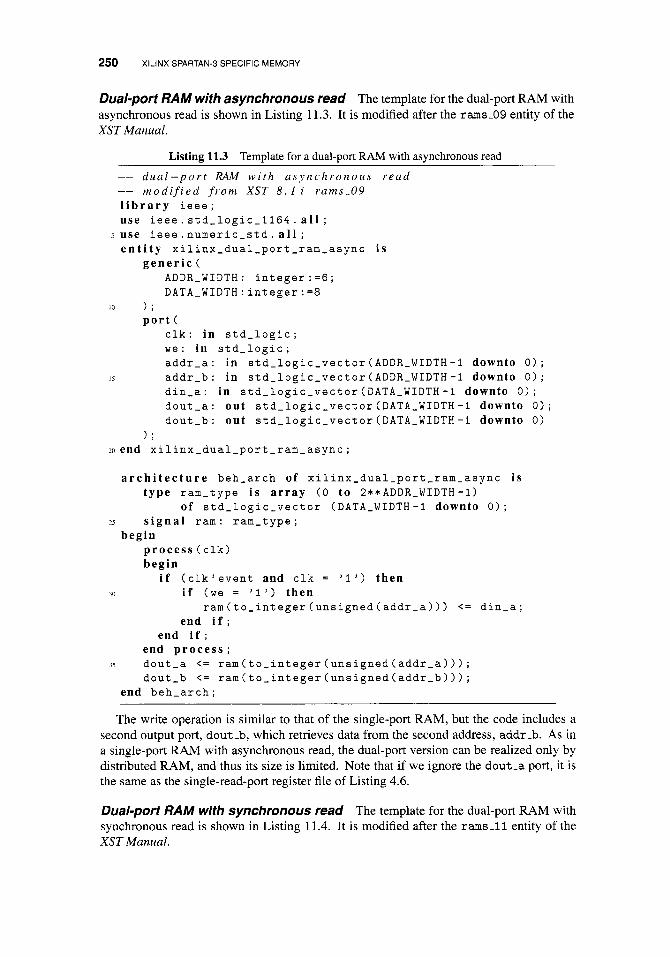
Dual-port RAM with asynchronous read The template for the dual-port RAM with asynchronous read is shown in Listing 11.3. It is modified after the rams-09 entity of the XST Manual.
Listing 11.3 Template for a dual-port RAM with asynchronous read
-- d u a l - p o r t RAM w i t h a s y n c h r o n o u s read __ m o d i f i e d f r o m X S T 8 . 1 i r a m s - 0 9 l i b r a r y ieee; use ieee. std-logic-1164. a l l ;
5 use ieee . numeric-std. a l l ; e n t i t y xilinx-dual-port -ram-async i s
g e n e r i c ( ADDR-WIDTH: integer :=6; DATA_WIDTH:integer:=8
10 ) ; port (
clk: in std-logic; we: in std-logic; addr-a: i n std-logic-vector (ADDR-WIDTH-1 downto 0 ) ; addr-b : in std-logic-vector (ADDR-WIDTH -1 downto 0 ) ; din-a: in std-logic-vector (DATA-WIDTH -1 downto 0 ) ; dout-a: out std-logic-vector (DATA-WIDTH -1 downto 0) ; dout-b : out std-logic-vector (DATA-WIDTH -1 downto 0 )
1 ; 20 end xilinx-dual-port-ram-async;
15
a r c h i t e c t u r e beh-arch of xilinx-dual-port-ram-async i s type ram-type i s array ( 0 t o 2**ADDR-WIDTH-l)
of std-logic-vector (DATA-WIDTH -1 downto 0) ; 25 s i g n a l ram: ram-type;
beg in p r o c e s s (clk) beg in
i f (clk’event and clk = ’1’) then 30 i f (we = ’1’) then
ram(to-integer(unsigned(addr-a))) <= din-a; end i f ;
end i f ; end p r o c e s s ;
35 dout-a <= ram(to-integer (unsigned(addr-a))); dout-b <= ram(to_integer(unsigned(addr-b));
end beh-arch ;
The write operation is similar to that of the single-port RAM, but the code includes a second output port, dout-b, which retrieves data from the second address, addr-b. As in a single-port RAM with asynchronous read, the dual-port version can be realized only by distributed RAM, and thus its size is limited. Note that if we ignore the dout-a port, it is the same as the single-read-port register file of Listing 4.6.
Dual-port RAM with synchronous read The template for the dual-port RAM with synchronous read is shown in Listing 11.4. It is modified after the rams-11 entity of the XST Manual.
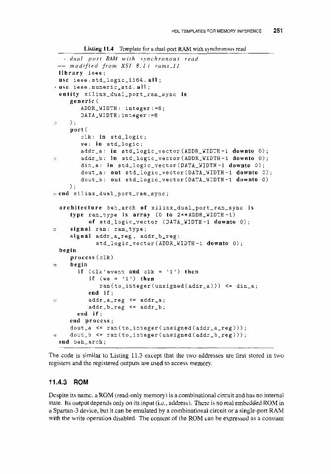
HDL TEMPLATES FOR MEMORY INFERENCE 251
Listing 11.4 Template for a dual-port RAM with synchronous read
-- d u a l - p o r t RAM w i t h s y n c h r o n o u s r e a d -- m o d i f i e d f r o m XST 8 . 1 i r a m s - 1 1 l i b r a r y ieee; use ieee. std-logic-1164. a l l ;
s use ieee. numeric-std. a l l ; e n t i t y xilinx-dual-port-ram-sync i s
g e n e r i c ( ADDR-WIDTH : DATA_WIDTH:integer:=8
integer : =6 ;
10 1 ; port (
clk: in std-logic; w e : in std-logic; addr-a: in std-logic-vector (ADDR-WIDTH -1 downto 0) ; addr-b: i n std-logic-vector (ADDR-WIDTH-1 downto 0) ; din-a: in std-logic-vector (DATA-WIDTH-1 downto 0 ) ; dout-a: out std-logic-vector (DATA-WIDTH-1 downto 0 ) ; dout-b : out std-logic-vector (DATA-WIDTH -1 downto 0 )
) ; 20 end xilinx-dual-port-ram-sync;
I S
a r c h i t e c t u r e beh-arch of xilinx-dual-port-ram-sync i s type ram-type i s array ( 0 to 2**ADDR-WIDTH-l)
of std-logic-vector (DATA-WIDTH-1 downto 0) ; 25 s i g n a l ram: ram-type;
s i g n a l addr-a-reg , addr-b-reg : std-logic-vector (ADDR-WIDTH -1 downto 0 ) ;
begin p r o c e s s (clk)
30 beg in i f (clk’event and clk = ’ 1 ’ ) then
i f (we = ’ 1 ’ ) then
end i f ; addr-a-reg <= addr-a; addr-b-reg <= addr-b ;
ram(to-integer(unsigned(addr-a))) <= din-a;
end i f ; end p r o c e s s ; dout-a <= rarn(to-integer(unsigned(addr-a-reg));
40 dout-b <= ram(to_integer(unsigned(addr-b-reg)); end beh-arch;
The code is similar to Listing 11.3 except that the two addresses are first stored in two registers and the registered outputs are used to access memory.
11.4.3 ROM
Despite its name, a ROM (read-only memory) is a combinational circuit and has no internal state. Its output depends only on its input (i.e., address). There is no real embedded ROM in a Spartan-3 device, but it can be emulated by a combinational circuit or a single-port RAM with the write operation disabled. The content of the ROM can be expressed as a constant
252 XlLlNX SPARTAN-3 SPECIFIC MEMORY
in the HDL code and the values are loaded to the RAM when the device is programmed. Since the ROM is based in a RAM, the read operation can be asynchronous or synchronous.
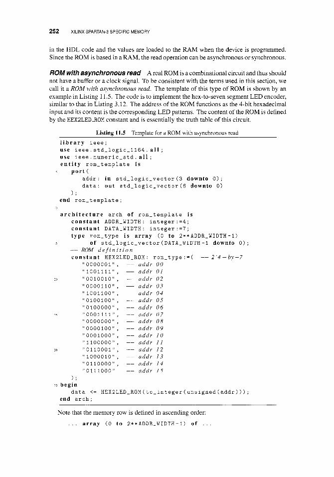
ROM with asynchronous read A real ROM is a combinational circuit and thus should not have a buffer or a clock signal. To be consistent with the terms used in this section, we call it a ROM with asynchronous read. The template of this type of ROM is shown by an example in Listing 11.5. The code is to implement the hex-to-seven segment LED encoder, similar to that in Listing 3.12. The address of the ROM functions as the 4-bit hexadecimal input and its content is the corresponding LED patterns. The content of the ROM is defined by the HEX2LEDAOM constant and is essentially the truth table of this circuit.
Listing 11.5 Template for a ROM with asynchronous read
l i b r a r y i e e e ; use i e e e . std-logic-1164. a l l ; use ieee. numeric-std. a l l ; e n t i t y rom-template i s
5 p o r t ( a d d r : i n std-logic-vector ( 3 downto 0) ; d a t a : out std-logic-vector (6 downto 0 )
1 ; end rom-template;
10
a r c h i t e c t u r e arch of rom-template i s c o n s t a n t ADDR-WIDTH: integer :=4; c o n s t a n t DATA-WIDTH: integer : = 7 ; t y p e rom-type i s array (0 t o 2**ADDR_WIDTH-l)
-- ROM d e f i n i t i o n c o n s t a n t HEXZLED-ROM: rom-type : = ( -- 2 ^ 4 - b y - 7
I 5 of std-logic-vector (DATA-WIDTH-1 downto 0 ) ;
"0000001", -- a d d r 00 "1001111", -- a d d r 0 1
10 "OOlOOlO", -- a d d r 0 2 "0000110", -- a d d r 0 3 " 1 0 0 1 1 0 0 " , -- a d d r 0 4 "0100100", -- a d d r 0 5 " 0 1 0 0 0 0 0 " , -- a d d r 0 6 " 0 0 0 1 1 1 1 " , -- a d d r 0 7 " 0 0 0 0 0 0 0 " , -- a d d r 0 8 " 0 0 0 0 1 0 0 " , -- a d d r 0 9 "OOOlOOO", -- a d d r 1 0 " 1 1 0 0 0 0 0 " , -- a d d r I 1
70 "0110001", -- a d d r 1 2 " 1 0 0 0 0 1 0 " , -- a d d r 1 3 " 0 1 1 0 0 0 0 " , -- a d d r 1 4 "0111000" -- a d d r 1 5
1 ; 35 b e g i n
data <= HEX2LED_ROM(to_integer(unsigned(addr))); end a r c h ;
Note that the memory row is defined in ascending order:
. . . a r r a y (0 t o Z**ADDR-WIDTH-I) of . . .
HDL TEMPLATES FOR MEMORY INFERENCE 253
and the first row of the HEX2LEDBOM constant corresponds to the address 00 of the ROM. The rows defined in the HEX2LEDBOM table must be reversed if the rom-type data type is defined in descending order:
. . a r r a y (2**ADDR-WIDTH-l downto 0) o f . . . Since there is no address or data buffer in this circuit, the ROM cannot be realized by a
block RAM. It is actually synthesized as a combinational circuit with the logic cells. The code can be considered as another form of a selected signal assignment or case statement. This type of ROM is feasible only for a small table. This code template is very general and is not specific to Xilinx devices.
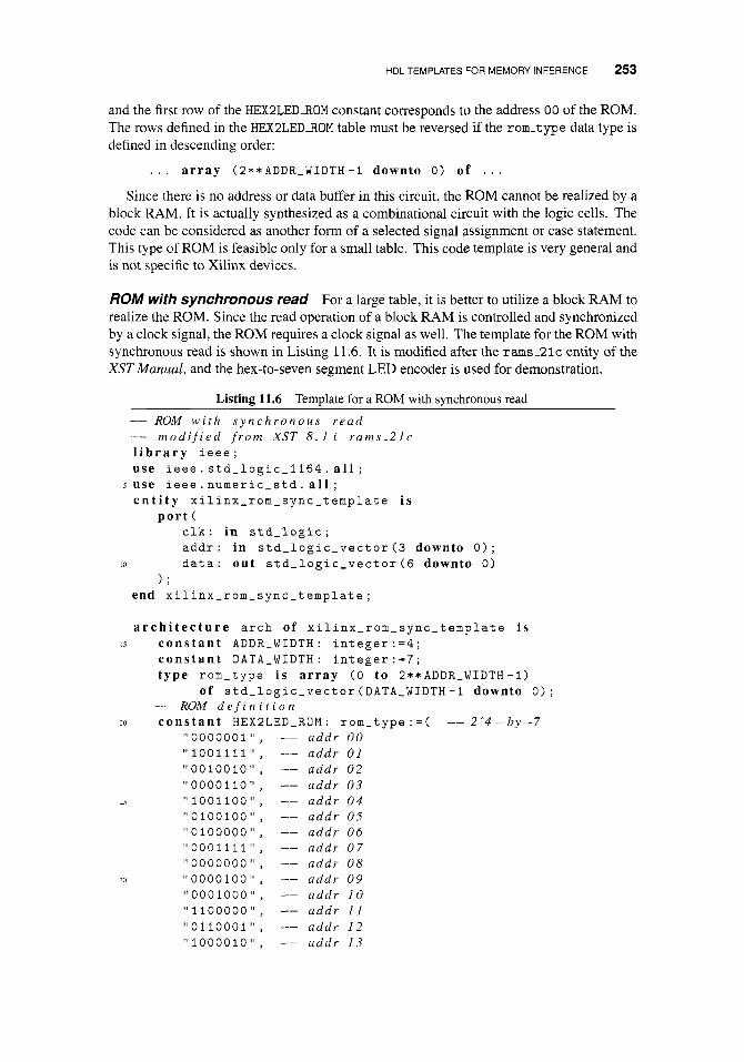
ROM with synchronous read For a large table, it is better to utilize a block RAM to realize the ROM. Since the read operation of a block RAM is controlled and synchronized by a clock signal, the ROM requires a clock signal as well. The template for the ROM with synchronous read is shown in Listing 11.6. It is modified after the r a m s - 2 l c entity of the XST Manual, and the hex-to-seven segment LED encoder is used for demonstration.
Listing 11.6 Template for a ROM with synchronous read
-- ROM with s y n c h r o n o u s r e a d -_ m o d i f i e d f r o m XST 8 . 1 i r a m s - 2 l c l i b r a r y ieee; use ieee . std-logic-1164. a l l ;
j use ieee. numeric-std. a l l ; e n t i t y xilinx-rom-sync-template i s
p o r t ( c l k : in std-logic; addr : i n std-logic-vector (3 downto 0 ) ;
10 data: out std-logic-vector (6 downto 0 )
) ; end xilinx-rom-sync-template;
a r c h i t e c t u r e arch of xilinx-rom- sync- t emplate i s 1 5 c o n s t a n t ADDR-WIDTH : integer : = 4 ;
c o n s t a n t DATA-WIDTH: integer : = 7 ; t y p e rom-type i s a r r a y ( 0 t o 2**ADDR_WIDTH-l)
-- ROM d e f i n i t i o n of std-logic-vector (DATA-WIDTH-1 downto 0 ) ;
20 c o n s t a n t HEX2LED-ROM: rom-type : = ( -- 2 * 4 - b y - 7 " 0 0 0 0 0 0 1 ~ ' , -- a d d r 0 0 "1001111", -- a d d r 01 "OOlOOlO", -- a d d r 0 2 " 0 0 0 0 1 1 0 " , -- a d d r 0 3
23 " 1 0 0 1 1 0 0 " , -- a d d r 0 4 " 0 1 0 0 1 0 0 " , -- a d d r 05 " 0 1 0 0 0 0 0 " , -- a d d r 06 " 0 0 0 1 1 1 1 " , -- a d d r 0 7 " 0 0 0 0 0 0 0 " , -- a d d r 0 8 "OOOOlOO", -- a d d r 0 9 " 0 0 0 1 0 0 0 " , -- a d d r 10 "llOOOOO", -- a d d r 1 1 "OllOOOl", -- a d d r 1 2 "lOOOOlO~', -- a d d r 1 3
30
254 XlLlNX SPARTAN-3 SPECIFIC MEMORY
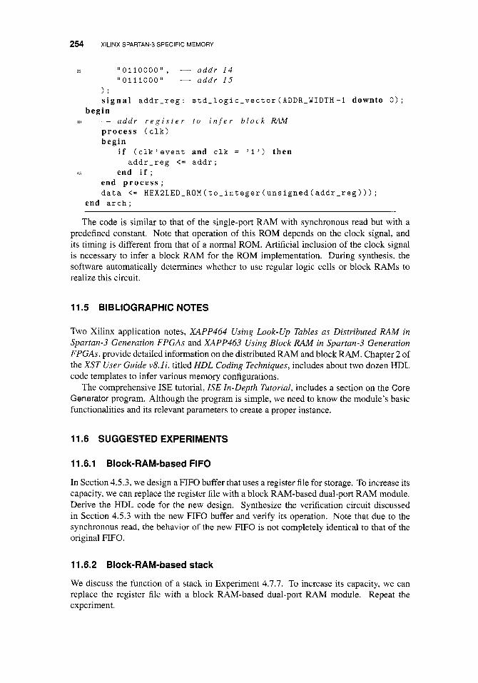
35 " 0 1 1 0 0 0 0 " , -- a d d r 1 4 " 0 11 1000 " -- a d d r 1 5
) ;
beg in s i g n a l addr-reg : std-logic-vector (ADDR-WIDTH -1 downto 0 ) ;
40 -- a d d r r e g i s t e r t o i n f e r b l o c k RAM p r o c e s s (clk) beg in
i f (clk'event and clk = '1') then addr-reg (= addr;
45 end i f ; end p r o c e s s ; data <= HEX2LED-ROM (to-integer (unsigned (addr-reg))) ;
end arch;
The code is similar to that of the single-port RAM with synchronous read but with a predefined constant. Note that operation of this ROM depends on the clock signal, and its timing is different from that of a normal ROM. Artificial inclusion of the clock signal is necessary to infer a block RAM for the ROM implementation. During synthesis, the software automatically determines whether to use regular logic cells or block RAMS to realize this circuit.
11.5 BIBLIOGRAPHIC NOTES
Two Xilinx application notes, XAPP464 Using Look-Up Tables as Distributed RAM in Spartan-3 Generation FPGAs and XAPP463 Using Block RAM in Spartan-3 Generation FPGAs, provide detailed information on the distributed RAM and block RAM. Chapter 2 of the XST User Guide v8.li, titled HDL Coding Techniques, includes about two dozen HDL code templates to infer various memory configurations.
The comprehensive ISE tutorial, ISE In-Depth Tutorial, includes a section on the Core Generator program. Although the program is simple, we need to know the module's basic functionalities and its relevant parameters to create a proper instance.
11.6 SUGGESTED EXPERIMENTS
11.6.1 Block-RAM-based FIFO
In Section 4.5.3, we design a FIFO buffer that uses a register file for storage. To increase its capacity, we can replace the register file with a block RAM-based dual-port RAM module. Derive the HDL code for the new design. Synthesize the verification circuit discussed in Section 4.5.3 with the new FIFO buffer and verify its operation. Note that due to the synchronous read, the behavior of the new FIFO is not completely identical to that of the original FIFO.
11.6.2 Block-RAM-based stack
We discuss the function of a stack in Experiment 4.7.7. To increase its capacity, we can replace the register file with a block RAM-based dual-port RAM module. Repeat the experiment.
SUGGESTED EXPERIMENTS 255
11.6.3 ROM-based sign-magnitude adder
We can implement any n-input, rn-output function with a 2"-by-m ROM. Consider the sign-magnitude adder discussed in Section 3.7.2 and assume that a and b are 4-bit input signals. Design this circuit as follows:
1. Write a program in a conventional programing language, such as C or Java, to
2. Follow the ROM template in Listing 11.5 to derive the HDL code. Cut and paste the
3. Synthesize the circuit and verify its operation. 4. Check the synthesis report and compare the sizes (in terms of the number of logic
5. Expand a and b to 8-bit input signals and repeat steps 1 to 4.
generate a 28-by-4 truth table for this circuit.
table to the code.
cells) of the original implementation and the ROM-based implementation.
11.6.4 ROM based sin(z) function
One way to implement a sinusoidal function, sin(z), is to use a look-up table. Assume that the desired implementation requires 10-bit input resolution [i.e., there are 1024 (21°) points between the input range of 0 and 2.1 and 8-bit output resolution [i.e., there are 256 (2') points between the output range of -1 and +1]. Let the input and output be the 10-bit z signal and the 8-bit y signal. The relationship between IC and y is
Y - = sin 27r- 27 ( ;o)
Because of the symmetry of the sin function, we only need to construct a 28-by-7 table for the first quadrant (i.e., between 0 and 4) and use simple pre- and postprocessing circuits to obtain the values in other quadrants. Design this circuit as follows:
1. Write a program in a conventional programming language to generate the 28-by-7
2. Follow the ROM template in Listing 11.6 to derive the HDL code for the look-up
3. Derive the complete HDL code. 4. Derive a testbench to generate the sinusoidal output for three complete periods. This
can be done by using a 10-bit counter to generate the 10-bit ROM address for 3 * 21° clock cycles. In ModelSim, we can display the y signal in Analog format to emulate the effect of a digital-to-analog converter.
table for the first quadrant.
table. Cut and paste the table to the code.
11.6.5 ROM-based sin(z) and cos(z) functions
In many communication modulation schemes, the sin(z) and C O S ( I C ) functions are needed at the same time. Assume that the format of the input and output is similar to that in Experiment 11.6.4. The new circuit has two outputs, ys and yc:
= sin (2.G) 27
27 - yc = cos (2.5)
Although we can follow the previous procedure and create a new ROM for the C O S ( I C )
function, a better alternative is to share the same ROM for both sin(z) and cos(z) functions.
256 XlLlNX SPARTAN-3 SPECIFIC MEMORY
This is based on the observations that cos(z) is only a phase shift of sin(z) and that the FPGA’s block RAM can provide dual-port access.
Note that this circuit requires essentially a “dual-port ROM.” No HDL behaviorial tem- plate is given for this type of memory. We need to experiment with HDL codes and to check the synthesis report to ensure that only one block RAM is inferred. It may be necessary to use the Core Generator program or direct HDL component instantiation to achieve this goal.
Construct this special ROM and derive the HDL code for the pre- and postprocessing circuits. Use a testbench similar to that in Experiment 1 1.6.4 to verify the circuit’s operation.