Embed Size (px)
Citation preview
Introduction to FPGA Design with Vivado High-Level Synthesis
UG998 (v1.0) July 2, 2013
Introduction to FPGA Design with Vivado HLS www.xilinx.com 2UG998 (v1.0) July 2, 2013
Notice of DisclaimerThe information disclosed to you hereunder (the “Materials”) is provided solely for the selection and use of Xilinx products. To the maximum extent permitted by applicable law: (1) Materials are made available "AS IS" and with all faults, Xilinx hereby DISCLAIMS ALL WARRANTIES AND CONDITIONS, EXPRESS, IMPLIED, OR STATUTORY, INCLUDING BUT NOT LIMITED TO WARRANTIES OF MERCHANTABILITY, NON-INFRINGEMENT, OR FITNESS FOR ANY PARTICULAR PURPOSE; and (2) Xilinx shall not be liable (whether in contract or tort, including negligence, or under any other theory of liability) for any loss or damage of any kind or nature related to, arising under, or in connection with, the Materials (including your use of the Materials), including for any direct, indirect, special, incidental, or consequential loss or damage (including loss of data, profits, goodwill, or any type of loss or damage suffered as a result of any action brought by a third party) even if such damage or loss was reasonably foreseeable or Xilinx had been advised of the possibility of the same. Xilinx assumes no obligation to correct any errors contained in the Materials or to notify you of updates to the Materials or to product specifications. You may not reproduce, modify, distribute, or publicly display the Materials without prior written consent. Certain products are subject to the terms and conditions of the Limited Warranties which can be viewed at http://www.xilinx.com/warranty.htm; IP cores may be subject to warranty and support terms contained in a license issued to you by Xilinx. Xilinx products are not designed or intended to be fail-safe or for use in any application requiring fail-safe performance; you assume sole risk and liability for use of Xilinx products in Critical Applications: http://www.xilinx.com/warranty.htm#critapps.© Copyright 2013 Xilinx, Inc. Xilinx, the Xilinx logo, Artix, ISE, Kintex, Spartan, Virtex, Vivado, Zynq, and other designated brands included herein are trademarks of Xilinx in the United States and other countries. AMBA, ARM, and Cortex are trademarks of ARM in the EU and other countries. PCI, PCIe, and PCI Express are trademarks of PCI-SIG and used under license. All other trademarks are the property of their respective owners.
Revision HistoryThe following table shows the revision history for this document.
Date Version Revision
07/02/2013 1.0 Initial Xilinx release.
Table of ContentsRevision History . . . . . . . . . . . . . . . . . . . . . . . . . . . . . . . . . . . . . . . . . . . . . . . . . . . . . . . . . . . . . . . . . . . . 2
Chapter 1: IntroductionOverview . . . . . . . . . . . . . . . . . . . . . . . . . . . . . . . . . . . . . . . . . . . . . . . . . . . . . . . . . . . . . . . . . . . . . . . . 5Programming Model . . . . . . . . . . . . . . . . . . . . . . . . . . . . . . . . . . . . . . . . . . . . . . . . . . . . . . . . . . . . . . . 6Guide Organization . . . . . . . . . . . . . . . . . . . . . . . . . . . . . . . . . . . . . . . . . . . . . . . . . . . . . . . . . . . . . . . . 8
Chapter 2: What is an FPGA?Overview . . . . . . . . . . . . . . . . . . . . . . . . . . . . . . . . . . . . . . . . . . . . . . . . . . . . . . . . . . . . . . . . . . . . . . . 11FPGA Architecture . . . . . . . . . . . . . . . . . . . . . . . . . . . . . . . . . . . . . . . . . . . . . . . . . . . . . . . . . . . . . . . . 11FPGA Parallelism Versus Processor Architectures . . . . . . . . . . . . . . . . . . . . . . . . . . . . . . . . . . . . . . . 17
Chapter 3: Basic Concepts of Hardware DesignOverview . . . . . . . . . . . . . . . . . . . . . . . . . . . . . . . . . . . . . . . . . . . . . . . . . . . . . . . . . . . . . . . . . . . . . . . 23Clock Frequency . . . . . . . . . . . . . . . . . . . . . . . . . . . . . . . . . . . . . . . . . . . . . . . . . . . . . . . . . . . . . . . . . . 23Latency and Pipelining. . . . . . . . . . . . . . . . . . . . . . . . . . . . . . . . . . . . . . . . . . . . . . . . . . . . . . . . . . . . . 27Throughput. . . . . . . . . . . . . . . . . . . . . . . . . . . . . . . . . . . . . . . . . . . . . . . . . . . . . . . . . . . . . . . . . . . . . . 28Memory Architecture and Layout. . . . . . . . . . . . . . . . . . . . . . . . . . . . . . . . . . . . . . . . . . . . . . . . . . . . 29
Chapter 4: Vivado High-Level SynthesisOverview . . . . . . . . . . . . . . . . . . . . . . . . . . . . . . . . . . . . . . . . . . . . . . . . . . . . . . . . . . . . . . . . . . . . . . . 32Operations . . . . . . . . . . . . . . . . . . . . . . . . . . . . . . . . . . . . . . . . . . . . . . . . . . . . . . . . . . . . . . . . . . . . . . 32Conditional Statements . . . . . . . . . . . . . . . . . . . . . . . . . . . . . . . . . . . . . . . . . . . . . . . . . . . . . . . . . . . . 35Loops. . . . . . . . . . . . . . . . . . . . . . . . . . . . . . . . . . . . . . . . . . . . . . . . . . . . . . . . . . . . . . . . . . . . . . . . . . . 36Functions . . . . . . . . . . . . . . . . . . . . . . . . . . . . . . . . . . . . . . . . . . . . . . . . . . . . . . . . . . . . . . . . . . . . . . . 38Dynamic Memory Allocation. . . . . . . . . . . . . . . . . . . . . . . . . . . . . . . . . . . . . . . . . . . . . . . . . . . . . . . . 38Pointers. . . . . . . . . . . . . . . . . . . . . . . . . . . . . . . . . . . . . . . . . . . . . . . . . . . . . . . . . . . . . . . . . . . . . . . . . 40
Chapter 5: Computation-Centric AlgorithmsOverview . . . . . . . . . . . . . . . . . . . . . . . . . . . . . . . . . . . . . . . . . . . . . . . . . . . . . . . . . . . . . . . . . . . . . . . 42Data Rate Optimization . . . . . . . . . . . . . . . . . . . . . . . . . . . . . . . . . . . . . . . . . . . . . . . . . . . . . . . . . . . . 44
Introduction to FPGA Design with Vivado HLS www.xilinx.com 3UG998 (v1.0) July 2, 2013
Chapter 6: Control-Centric AlgorithmsOverview . . . . . . . . . . . . . . . . . . . . . . . . . . . . . . . . . . . . . . . . . . . . . . . . . . . . . . . . . . . . . . . . . . . . . . . 50Expressing Control in C/C++ . . . . . . . . . . . . . . . . . . . . . . . . . . . . . . . . . . . . . . . . . . . . . . . . . . . . . . . . 50UDP Packet Processing . . . . . . . . . . . . . . . . . . . . . . . . . . . . . . . . . . . . . . . . . . . . . . . . . . . . . . . . . . . . 55
Chapter 7: Software Verification and Vivado HLSOverview . . . . . . . . . . . . . . . . . . . . . . . . . . . . . . . . . . . . . . . . . . . . . . . . . . . . . . . . . . . . . . . . . . . . . . . 60Software Test Bench . . . . . . . . . . . . . . . . . . . . . . . . . . . . . . . . . . . . . . . . . . . . . . . . . . . . . . . . . . . . . . 60Code Coverage . . . . . . . . . . . . . . . . . . . . . . . . . . . . . . . . . . . . . . . . . . . . . . . . . . . . . . . . . . . . . . . . . . . 62Uninitialized Variables. . . . . . . . . . . . . . . . . . . . . . . . . . . . . . . . . . . . . . . . . . . . . . . . . . . . . . . . . . . . . 63Out-of-Bounds Memory Access . . . . . . . . . . . . . . . . . . . . . . . . . . . . . . . . . . . . . . . . . . . . . . . . . . . . . 64Co-Simulation. . . . . . . . . . . . . . . . . . . . . . . . . . . . . . . . . . . . . . . . . . . . . . . . . . . . . . . . . . . . . . . . . . . . 65When C/C++ Verification Is Not Possible . . . . . . . . . . . . . . . . . . . . . . . . . . . . . . . . . . . . . . . . . . . . . . 67
Chapter 8: Integration of Multiple ProgramsOverview . . . . . . . . . . . . . . . . . . . . . . . . . . . . . . . . . . . . . . . . . . . . . . . . . . . . . . . . . . . . . . . . . . . . . . . 68AXI. . . . . . . . . . . . . . . . . . . . . . . . . . . . . . . . . . . . . . . . . . . . . . . . . . . . . . . . . . . . . . . . . . . . . . . . . . . . . 68Design Example: Application Running on a Zynq-7000 AP SoC . . . . . . . . . . . . . . . . . . . . . . . . . . . . 72
Chapter 9: Verification of a Complete ApplicationOverview . . . . . . . . . . . . . . . . . . . . . . . . . . . . . . . . . . . . . . . . . . . . . . . . . . . . . . . . . . . . . . . . . . . . . . . 83Standalone Compute Systems . . . . . . . . . . . . . . . . . . . . . . . . . . . . . . . . . . . . . . . . . . . . . . . . . . . . . . 83Processor-Based Systems . . . . . . . . . . . . . . . . . . . . . . . . . . . . . . . . . . . . . . . . . . . . . . . . . . . . . . . . . . 86
Appendix A: Additional ResourcesXilinx Resources . . . . . . . . . . . . . . . . . . . . . . . . . . . . . . . . . . . . . . . . . . . . . . . . . . . . . . . . . . . . . . . . . . 89Solution Centers. . . . . . . . . . . . . . . . . . . . . . . . . . . . . . . . . . . . . . . . . . . . . . . . . . . . . . . . . . . . . . . . . . 89References . . . . . . . . . . . . . . . . . . . . . . . . . . . . . . . . . . . . . . . . . . . . . . . . . . . . . . . . . . . . . . . . . . . . . . 89
Introduction to FPGA Design with Vivado HLS www.xilinx.com 4UG998 (v1.0) July 2, 2013
Chapter 1
Introduction
OverviewSoftware is the basis of all applications. Whether for entertainment, gaming, communications, or medicine, many of the products people use today began as a software model or prototype. Based on the performance and programmability constraints of the system, the software engineer is tasked with determining the best implementation platform to get a project to market. To accomplish this task, the software engineer is aided by both programming techniques and a variety of hardware processing platforms.
On the programming side, previous decades yielded advances in object-oriented programming for code reuse and parallel computing paradigms for boosting algorithm performance. The advancements in programming languages, frameworks, and tools allowed the software engineer to quickly prototype and test different approaches to solve a particular problem. This need to quickly prototype a solution leads to two interesting questions. The first question of how to analyze and quantify one algorithm against another is extensively discussed in other works and is not the focus of this guide. The second question of where to execute the algorithm is addressed in this guide in relation to f ield programmable gate arrays (FPGAs).
Regarding where to run an algorithm, there is an increasing focus on parallelization and concurrency. Although the interest in the parallel and concurrent execution of software programs is not new, the renewed and increased interest is aided by certain trends in processor and application-specif ic integrated circuit (ASIC) design. In the past, the software engineer faced two choices for getting more performance out of a software algorithm: a custom-integrated circuit or an FPGA.
The first and most expensive option is to turn the algorithm over to a hardware engineer for a custom circuit implementation. The cost of this option is based on:
• Cost to fabricate the circuit
• Time to translate the algorithm into hardware
Despite advancements in fabrication process node technology that have yielded signif icant improvements in power consumption, computational throughput, and logic density, the cost to fabricate a custom-integrated circuit or ASIC for an application is still high. At each processing node, the cost of fabrication continues to increase to the point where this
Introduction to FPGA Design with Vivado HLS www.xilinx.com 5UG998 (v1.0) July 2, 2013
Programming Model
approach is only economically viable for applications that ship in the range of millions of units.
The second option is to use an FPGA, which addresses the cost issues inherent in ASIC fabrication. FPGAs allow the designer to create a custom circuit implementation of an algorithm using an off-the-shelf component composed of basic programmable logic elements. This platform offers the power consumption savings and performance benefits of smaller fabrication nodes without incurring the cost and complexity of an ASIC development effort. Similar to an ASIC, an algorithm implemented in an FPGA benefits from the inherent parallel nature of a custom circuit.
Programming ModelThe programming model of a hardware platform is one of the driving factors behind its adoption. Software algorithms are typically captured in C/C++ or some other high-level language, which abstracts the details of the computing platform. These languages allow for quick iteration, incremental improvements, and code portability, which are critical to the software engineer. For the past few decades, the fast execution of algorithms captured in these languages have fueled the development of processors and software compilers.
Initially, improving the runtime of software was based on two central concepts: increasing processor clock frequency and using specialized processors. For many years, it was common practice to wait a year for the next generation processor as a way to speed up execution. At every new higher clock frequency, the software program ran faster. Although this was acceptable in some cases, for a large set of applications, incremental speedup through processor clock frequency is not enough to deliver a viable product to market.
For this type of application, the specialized processor was created. Although there are many kinds of specialized processors, such as the digital signal processor (DSP) and graphics processing unit (GPU), all of these processors are capable of executing an algorithm written in a high-level language, such as C, and have function-specif ic accelerators to improve the execution of their target software applications.
With the recent paradigm shift in the design of standard and specialized processors, both types of processors stopped relying on clock frequency increases for program speedup and added more processing cores per chip. Multicore processors put program parallelization at the forefront of techniques used to boost software performance. The software engineer must now structure algorithms in a way that leads to efficient parallelization for performance. The techniques required in algorithm design use the same base elements of FPGA design. The main difference between an FPGA and a processor is the programming model.
Introduction to FPGA Design with Vivado HLS www.xilinx.com 6UG998 (v1.0) July 2, 2013
Programming Model
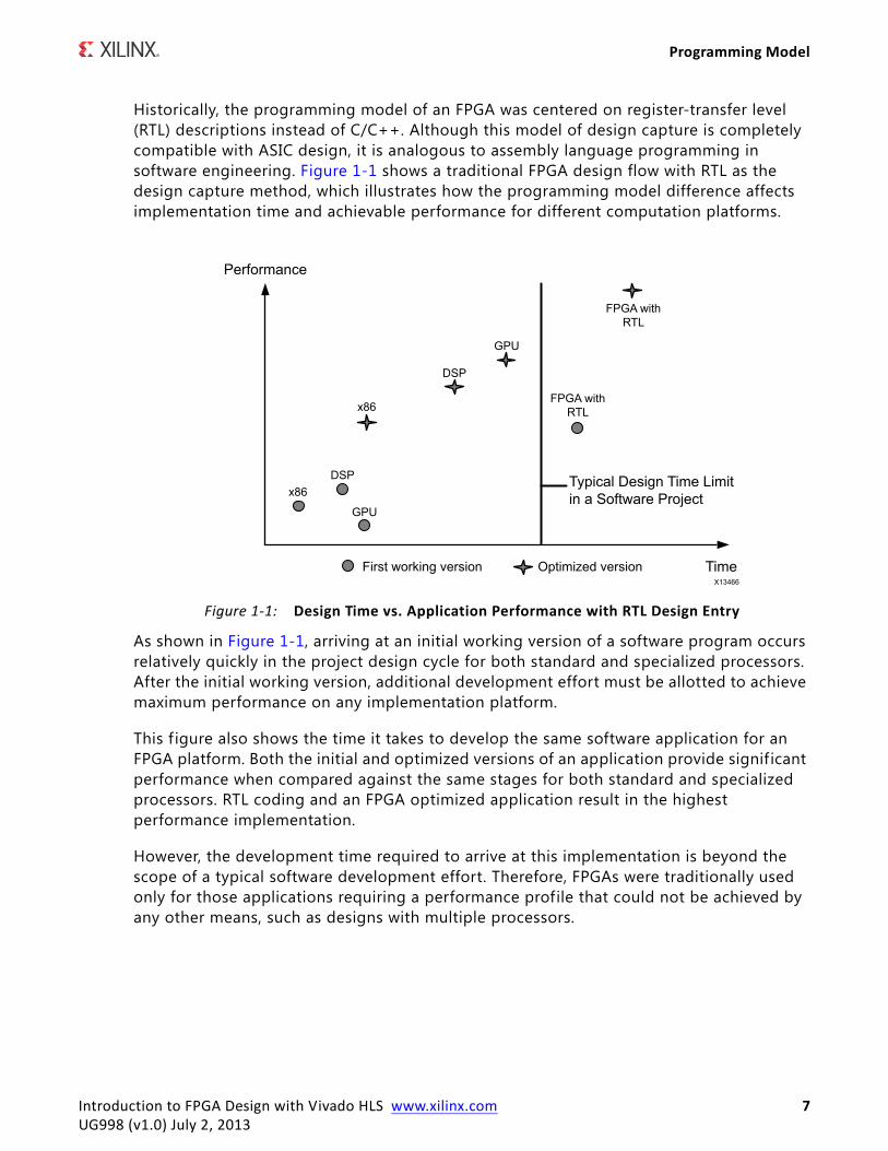
Historically, the programming model of an FPGA was centered on register-transfer level (RTL) descriptions instead of C/C++. Although this model of design capture is completely compatible with ASIC design, it is analogous to assembly language programming in software engineering. Figure 1-1 shows a traditional FPGA design flow with RTL as the design capture method, which illustrates how the programming model difference affects implementation time and achievable performance for different computation platforms.
As shown in Figure 1-1, arriving at an initial working version of a software program occurs relatively quickly in the project design cycle for both standard and specialized processors. After the initial working version, additional development effort must be allotted to achieve maximum performance on any implementation platform.
This f igure also shows the time it takes to develop the same software application for an FPGA platform. Both the initial and optimized versions of an application provide signif icant performance when compared against the same stages for both standard and specialized processors. RTL coding and an FPGA optimized application result in the highest performance implementation.
However, the development time required to arrive at this implementation is beyond the scope of a typical software development effort. Therefore, FPGAs were traditionally used only for those applications requiring a performance profile that could not be achieved by any other means, such as designs with multiple processors.
X-Ref Target - Figure 1-1
Figure 1-1: Design Time vs. Application Performance with RTL Design Entry
Introduction to FPGA Design with Vivado HLS www.xilinx.com 7UG998 (v1.0) July 2, 2013
Guide Organization
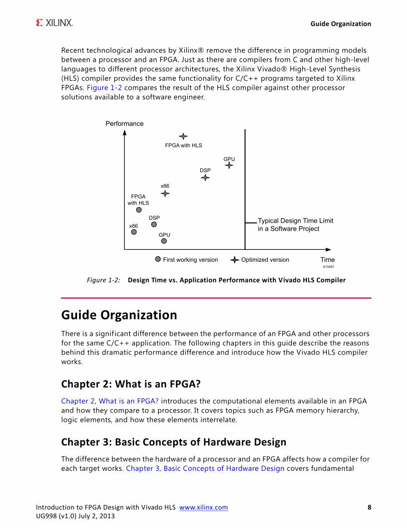
Recent technological advances by Xilinx® remove the difference in programming models between a processor and an FPGA. Just as there are compilers from C and other high-level languages to different processor architectures, the Xilinx Vivado® High-Level Synthesis (HLS) compiler provides the same functionality for C/C++ programs targeted to Xilinx FPGAs. Figure 1-2 compares the result of the HLS compiler against other processor solutions available to a software engineer.
Guide OrganizationThere is a signif icant difference between the performance of an FPGA and other processors for the same C/C++ application. The following chapters in this guide describe the reasons behind this dramatic performance difference and introduce how the Vivado HLS compiler works.
Chapter 2: What is an FPGA?Chapter 2, What is an FPGA? introduces the computational elements available in an FPGA and how they compare to a processor. It covers topics such as FPGA memory hierarchy, logic elements, and how these elements interrelate.
Chapter 3: Basic Concepts of Hardware DesignThe difference between the hardware of a processor and an FPGA affects how a compiler for each target works. Chapter 3, Basic Concepts of Hardware Design covers fundamental
X-Ref Target - Figure 1-2
Figure 1-2: Design Time vs. Application Performance with Vivado HLS Compiler
Introduction to FPGA Design with Vivado HLS www.xilinx.com 8UG998 (v1.0) July 2, 2013
Guide Organization
hardware concepts that apply to both FPGA and processor-based designs. Understanding these concepts assists the designer in guiding the Vivado HLS compiler to create the best processing architecture.
Chapter 4: Vivado High-Level SynthesisChapter 4, Vivado High-Level Synthesis introduces the Xilinx Vivado HLS compiler. Using concepts from the preceding two chapters, this section describes how a C/C++ program is compiled for an FPGA. This chapter focuses on how the compiler extracts parallelism, organizes memory, and connects multiple programs within an FPGA.
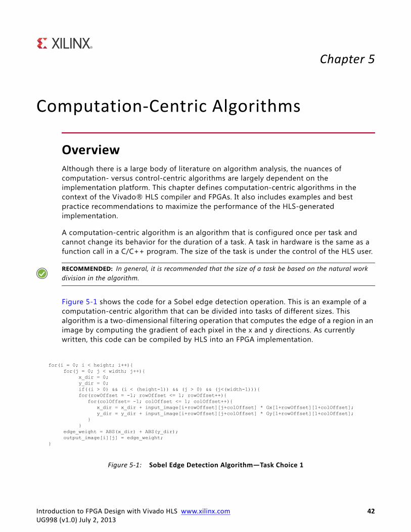
Chapter 5: Computation-Centric AlgorithmsAlthough there is extensive literature on algorithm analysis, the nuances of computation- versus control-centric algorithms are largely dependent on the implementation platform. Chapter 5, Computation-Centric Algorithms defines computation-centric algorithms for an FPGA and provides examples and best practice recommendations.
Chapter 6: Control-Centric AlgorithmsControl-centric algorithms can be implemented on both processors and FPGAs. The implementation choice depends on the reaction time required of the algorithm. Chapter 6, Control-Centric Algorithms provides an overview of control-centric algorithm implementation options and provides a networking example for user datagram protocol (UDP) packet processing.
Chapter 7: Software Verification and Vivado HLSAs with all compilers, the quality and correctness of the HLS compiler output depends on the input software. Chapter 7, Software Verif ication and Vivado HLS reviews recommended software quality techniques that apply to the Vivado HLS compiler. It presents examples of typical coding errors and their effect on HLS compilation as well as possible solutions to each problem. It also includes a section on what to do when program behavior cannot be fully verif ied at the C level.
Chapter 8: Integration of Multiple ProgramsJust as most processors run multiple programs to execute an application, an FPGA can also build multiple programs or modules to execute a specif ic application. Chapter 8, Integration of Multiple Programs describes how to connect multiple modules in an FPGA and how to control these modules with a processor. It highlights the Xilinx Zynq®-7000 All Programmable (AP) System on a Chip (SoC), which combines FPGA fabric with ARM® Cortex™-A9 processors. Using both a consumer and producer example, this chapter also demonstrates complete system development, integration, and design trade-offs.
Introduction to FPGA Design with Vivado HLS www.xilinx.com 9UG998 (v1.0) July 2, 2013
Guide Organization
Chapter 9: Verification of a Complete ApplicationWith an FPGA, a complete application creates a hardware system. This system can have one or more modules in the FPGA fabric as well as code executing on a processor. Chapter 9, Verif ication of a Complete Application provides recommendations and best practices to ensure correct execution of the target application.
Introduction to FPGA Design with Vivado HLS www.xilinx.com 10UG998 (v1.0) July 2, 2013
Chapter 2
What is an FPGA?
OverviewAn FPGA is a type of integrated circuit (IC) that can be programmed for different algorithms after fabrication. Modern FPGA devices consist of up to two million logic cells that can be configured to implement a variety of software algorithms. Although the traditional FPGA design flow is more similar to a regular IC than a processor, an FPGA provides significant cost advantages in comparison to an IC development effort and offers the same level of performance in most cases. Another advantage of the FPGA when compared to the IC is its ability to be dynamically reconfigured. This process, which is the same as loading a program in a processor, can affect part or all of the resources available in the FPGA fabric.
When using the Vivado® HLS compiler, it is important to have a basic understanding of the available resources in the FPGA fabric and how they interact to execute a target application. This chapter presents fundamental information about FPGAs, which is required to guide HLS to the best computational architecture for any algorithm.
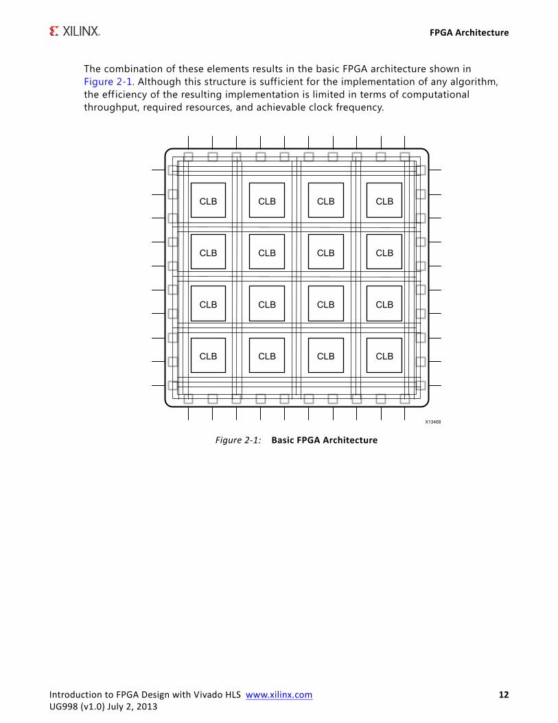
FPGA ArchitectureThe basic structure of an FPGA is composed of the following elements:
• Look-up table (LUT): This element performs logic operations.
• Flip-Flop (FF): This register element stores the result of the LUT.
• Wires: These elements connect elements to one another.
• Input/Output (I/O) pads: These physically available ports get data in and out of the FPGA.
Introduction to FPGA Design with Vivado HLS www.xilinx.com 11UG998 (v1.0) July 2, 2013
FPGA Architecture
The combination of these elements results in the basic FPGA architecture shown in Figure 2-1. Although this structure is sufficient for the implementation of any algorithm, the eff iciency of the resulting implementation is limited in terms of computational throughput, required resources, and achievable clock frequency.
X-Ref Target - Figure 2-1
Figure 2-1: Basic FPGA Architecture
Introduction to FPGA Design with Vivado HLS www.xilinx.com 12UG998 (v1.0) July 2, 2013
FPGA Architecture
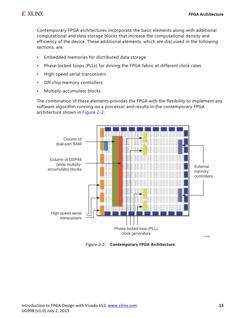
Contemporary FPGA architectures incorporate the basic elements along with additional computational and data storage blocks that increase the computational density and eff iciency of the device. These additional elements, which are discussed in the following sections, are:
• Embedded memories for distributed data storage
• Phase-locked loops (PLLs) for driving the FPGA fabric at different clock rates
• High-speed serial transceivers
• Off-chip memory controllers
• Multiply-accumulate blocks
The combination of these elements provides the FPGA with the flexibility to implement any software algorithm running on a processor and results in the contemporary FPGA architecture shown in Figure 2-2.
X-Ref Target - Figure 2-2
Figure 2-2: Contemporary FPGA Architecture
Introduction to FPGA Design with Vivado HLS www.xilinx.com 13UG998 (v1.0) July 2, 2013
FPGA Architecture
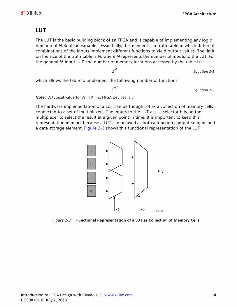
LUTThe LUT is the basic building block of an FPGA and is capable of implementing any logic function of N Boolean variables. Essentially, this element is a truth table in which different combinations of the inputs implement different functions to yield output values. The limit on the size of the truth table is N, where N represents the number of inputs to the LUT. For the general N-input LUT, the number of memory locations accessed by the table is:
Equation 2-1
which allows the table to implement the following number of functions:
Equation 2-2
Note: A typical value for N in Xilinx FPGA devices is 6.
The hardware implementation of a LUT can be thought of as a collection of memory cells connected to a set of multiplexers. The inputs to the LUT act as selector bits on the multiplexer to select the result at a given point in time. It is important to keep this representation in mind, because a LUT can be used as both a function compute engine and a data storage element. Figure 2-3 shows this functional representation of the LUT.
X-Ref Target - Figure 2-3
Figure 2-3: Functional Representation of a LUT as Collection of Memory Cells
2N
2NN
Introduction to FPGA Design with Vivado HLS www.xilinx.com 14UG998 (v1.0) July 2, 2013
FPGA Architecture
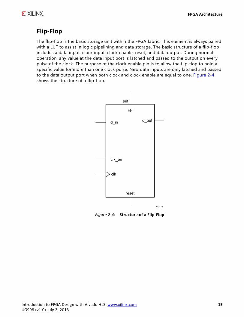
Flip-FlopThe flip-flop is the basic storage unit within the FPGA fabric. This element is always paired with a LUT to assist in logic pipelining and data storage. The basic structure of a flip-flop includes a data input, clock input, clock enable, reset, and data output. During normal operation, any value at the data input port is latched and passed to the output on every pulse of the clock. The purpose of the clock enable pin is to allow the flip-flop to hold a specific value for more than one clock pulse. New data inputs are only latched and passed to the data output port when both clock and clock enable are equal to one. Figure 2-4 shows the structure of a flip-flop.
X-Ref Target - Figure 2-4
Figure 2-4: Structure of a Flip-Flop
Introduction to FPGA Design with Vivado HLS www.xilinx.com 15UG998 (v1.0) July 2, 2013
FPGA Architecture
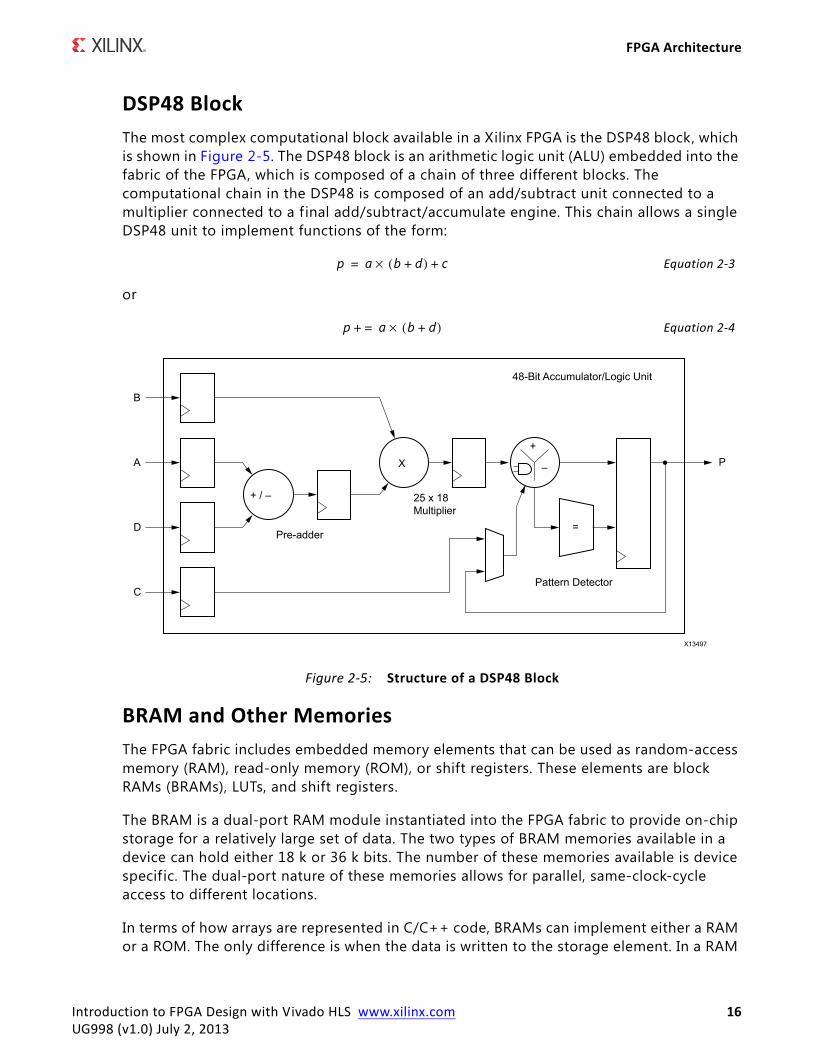
DSP48 BlockThe most complex computational block available in a Xilinx FPGA is the DSP48 block, which is shown in Figure 2-5. The DSP48 block is an arithmetic logic unit (ALU) embedded into the fabric of the FPGA, which is composed of a chain of three different blocks. The computational chain in the DSP48 is composed of an add/subtract unit connected to a multiplier connected to a final add/subtract/accumulate engine. This chain allows a single DSP48 unit to implement functions of the form:
Equation 2-3
or
Equation 2-4
BRAM and Other MemoriesThe FPGA fabric includes embedded memory elements that can be used as random-access memory (RAM), read-only memory (ROM), or shift registers. These elements are block RAMs (BRAMs), LUTs, and shift registers.
The BRAM is a dual-port RAM module instantiated into the FPGA fabric to provide on-chip storage for a relatively large set of data. The two types of BRAM memories available in a device can hold either 18 k or 36 k bits. The number of these memories available is device specific. The dual-port nature of these memories allows for parallel, same-clock-cycle access to different locations.
In terms of how arrays are represented in C/C++ code, BRAMs can implement either a RAM or a ROM. The only difference is when the data is written to the storage element. In a RAM
X-Ref Target - Figure 2-5
Figure 2-5: Structure of a DSP48 Block
p a b d+( )× c+=
p a b d+( )×=+
Introduction to FPGA Design with Vivado HLS www.xilinx.com 16UG998 (v1.0) July 2, 2013
FPGA Parallelism Versus Processor Architectures
configuration, the data can be read and written at any time during the runtime of the circuit. In contrast, in a ROM configuration, data can only be read during the runtime of the circuit. The data of the ROM is written as part of the FPGA configuration and cannot be modif ied in any way.
As previously discussed, the LUT is a small memory in which the contents of a truth table are written during device configuration. Due to the flexibility of the LUT structure in Xilinx FPGAs, these blocks can be used as 64-bit memories and are commonly referred to as distributed memories. This is the fastest kind of memory available on the FPGA device, because it can be instantiated in any part of the fabric that improves the performance of the implemented circuit.
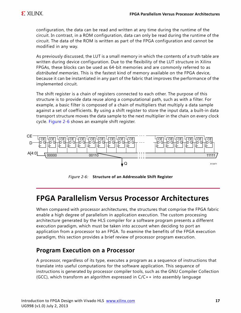
The shift register is a chain of registers connected to each other. The purpose of this structure is to provide data reuse along a computational path, such as with a filter. For example, a basic f ilter is composed of a chain of multipliers that multiply a data sample against a set of coeff icients. By using a shift register to store the input data, a built-in data transport structure moves the data sample to the next multiplier in the chain on every clock cycle. Figure 2-6 shows an example shift register.
FPGA Parallelism Versus Processor ArchitecturesWhen compared with processor architectures, the structures that comprise the FPGA fabric enable a high degree of parallelism in application execution. The custom processing architecture generated by the HLS compiler for a software program presents a different execution paradigm, which must be taken into account when deciding to port an application from a processor to an FPGA. To examine the benefits of the FPGA execution paradigm, this section provides a brief review of processor program execution.
Program Execution on a ProcessorA processor, regardless of its type, executes a program as a sequence of instructions that translate into useful computations for the software application. This sequence of instructions is generated by processor compiler tools, such as the GNU Compiler Collection (GCC), which transform an algorithm expressed in C/C++ into assembly language
X-Ref Target - Figure 2-6
Figure 2-6: Structure of an Addressable Shift Register
Introduction to FPGA Design with Vivado HLS www.xilinx.com 17UG998 (v1.0) July 2, 2013
FPGA Parallelism Versus Processor Architectures
constructs that are native to the processor. The job of a processor compiler is to take a C function of the form:
Equation 2-5
and transform it into assembly code as follows:
The assembly code in Figure 2-7 defines the addition operation to compute the value of z in terms of the internal registers of a processor. The code states that the input values for the computation are stored in registers R1 and R2, and the result of the computation is stored in register R3. This code is simple, and it does not express all the instructions needed to compute the value of z. This code only handles the computation after the data has arrived at the processor. Therefore, the compiler must create additional assembly language instructions to load the registers of the processor with data from a central memory and to write back the result to memory. The complete assembly program to compute the value of z is as follows:
The code in Figure 2-8 shows that even a simple operation, such as the addition of two values, results in multiple assembly instructions. The computational latency of each instruction is not equal across instruction types. For example, depending on the location of a and b, the LD operations take a different number of clock cycles to complete. If the values are in the processor cache, these load operations complete within a few tens of clock cycles. If the values are in the main, double data rate (DDR) memory, the operations take between hundreds and thousands of clock cycles to complete. If the values are in a hard drive, the load operations take even longer to complete. This is why software engineers with cache hit traces spend so much time restructuring their algorithms to increase the spatial locality of data in memory to increase the cache hit rate and decrease the processor time spent per instruction.
IMPORTANT: The level of effort required by the software engineer in restructuring algorithms to better fit the available processor cache is not required when the same operation is implemented in an FPGA.
X-Ref Target - Figure 2-7
Figure 2-7: Computation Expressed Assembly Code
X-Ref Target - Figure 2-8
Figure 2-8: Complete Assembly Program to Compute Z
z a b;+=
Introduction to FPGA Design with Vivado HLS www.xilinx.com 18UG998 (v1.0) July 2, 2013
FPGA Parallelism Versus Processor Architectures
Program Execution on an FPGAThe FPGA is an inherently parallel processing fabric capable of implementing any logical and arithmetic function that can run on a processor. The main difference is that the HLS compiler, which is used to transform software descriptions into RTL, is not hindered by the restrictions of a cache and a unif ied memory space.
The computation of z is compiled by HLS into several LUTs required to achieve the size of the output operand. For example, assume that in the original software program the variable a, b, and z are defined with the short data type. This type, which defines a 16-bit data container, gets implemented as 16 LUTs by HLS.
Note: As a general rule, 1 LUT is equivalent to 1 bit of computation.
The LUTs used for the computation of z are exclusive to this operation only. Unlike a processor, where all computations share the same ALU, an FPGA implementation instantiates independent sets of LUTs for each computation in the software algorithm.
In addition to assigning unique LUT resources per computation, the FPGA differs from a processor in both memory architecture and the cost of memory accesses. In an FPGA implementation, the HLS compiler arranges memories into multiple storage banks as close as possible to the point of use in the operation. This results in an instantaneous memory bandwidth, which far exceeds the capabilities of a processor. For example, the Xilinx Kintex®-7 410T device has a total of 1,590 18 k-bit BRAMs available. In terms of memory bandwidth, the memory layout of this device provides the software engineer with the capacity of 0.5M-bits per second at the register level and 23T-bits per second at the BRAM level.
With regard to computational throughput and memory bandwidth, the HLS compiler exercises the capabilities of the FPGA fabric through the processes of scheduling, pipelining, and dataflow. Although transparent to the user, these processes are integral stages of the software compilation process that extract the best possible circuit-level implementation of the software application.
Scheduling
Scheduling is the process of identifying the data and control dependencies between different operations to determine when each will execute. In traditional FPGA design, this is a manual process also referred to as parallelizing the software algorithm for a hardware implementation.
HLS analyzes dependencies between adjacent operations as well as across time. This allows the compiler to group operations to execute in the same clock cycle and to set up the hardware to allow the overlap of function calls. The overlap of function call executions removes the processor restriction that requires the current function call to fully complete before the next function call to the same set of operations can begin. This process is called pipelining and is covered in detail in the following section and remaining chapters.
Introduction to FPGA Design with Vivado HLS www.xilinx.com 19UG998 (v1.0) July 2, 2013
FPGA Parallelism Versus Processor Architectures
Pipelining
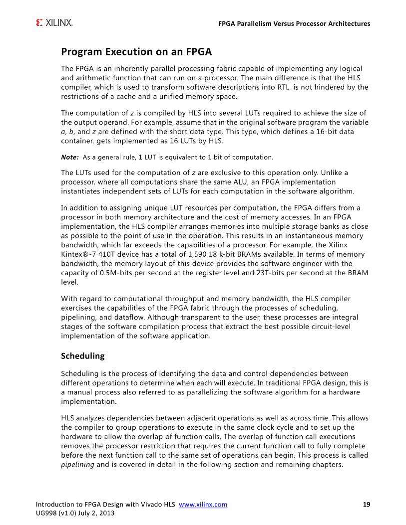
Pipelining is a digital design technique that allows the designer to avoid data dependencies and increase the level of parallelism in an algorithm hardware implementation. The data dependence in the original software implementation is preserved for functional equivalence, but the required circuit is divided into a chain of independent stages. All stages in the chain run in parallel on the same clock cycle. The only difference is the source of data for each stage. Each stage in the computation receives its data values from the result computed by the preceding stage during the previous clock cycle. For example, to compute the following function the HLS compiler instantiates one multiplier and two adder blocks:
Equation 2-6
Figure 2-9 shows this compute structure and the effects of pipelining. It shows two implementations of the example function. The top implementation is the datapath required to compute the result y without pipelining. This implementation behaves similarly to the corresponding C/C++ function in that all input values must be known at the start of the computation, and only one result y can be computed at a time. The bottom implementation shows the pipelined version of the same circuit.
The boxes in the datapath in Figure 2-9 represent registers that are implemented by flip-flop blocks in the FPGA fabric. Each box can be counted as a single clock cycle. Therefore, in the pipelined version, the computation of each result y takes three clock
X-Ref Target - Figure 2-9
Figure 2-9: FPGA Implementation of a Compute Function
y a x×( ) b c+ +=
Introduction to FPGA Design with Vivado HLS www.xilinx.com 20UG998 (v1.0) July 2, 2013
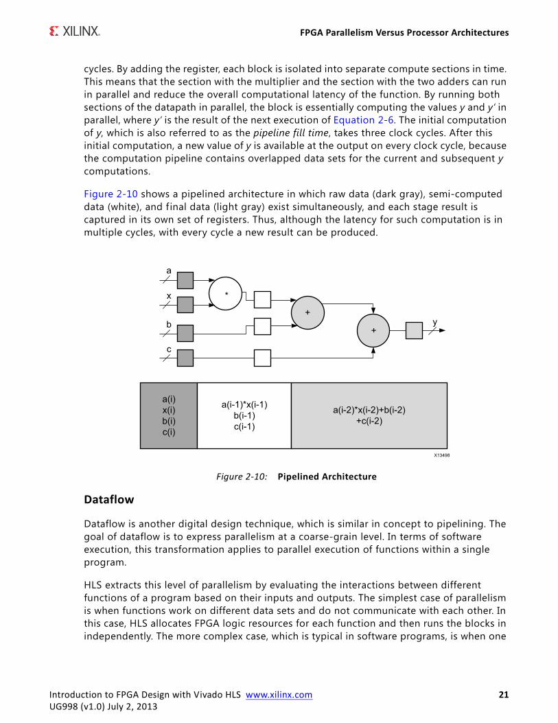
FPGA Parallelism Versus Processor Architectures
cycles. By adding the register, each block is isolated into separate compute sections in time. This means that the section with the multiplier and the section with the two adders can run in parallel and reduce the overall computational latency of the function. By running both sections of the datapath in parallel, the block is essentially computing the values y and y’ in parallel, where y’ is the result of the next execution of Equation 2-6. The initial computation of y, which is also referred to as the pipeline fill time, takes three clock cycles. After this initial computation, a new value of y is available at the output on every clock cycle, because the computation pipeline contains overlapped data sets for the current and subsequent y computations.
Figure 2-10 shows a pipelined architecture in which raw data (dark gray), semi-computed data (white), and f inal data (light gray) exist simultaneously, and each stage result is captured in its own set of registers. Thus, although the latency for such computation is in multiple cycles, with every cycle a new result can be produced.
Dataflow
Dataflow is another digital design technique, which is similar in concept to pipelining. The goal of dataflow is to express parallelism at a coarse-grain level. In terms of software execution, this transformation applies to parallel execution of functions within a single program.
HLS extracts this level of parallelism by evaluating the interactions between different functions of a program based on their inputs and outputs. The simplest case of parallelism is when functions work on different data sets and do not communicate with each other. In this case, HLS allocates FPGA logic resources for each function and then runs the blocks in independently. The more complex case, which is typical in software programs, is when one
X-Ref Target - Figure 2-10
Figure 2-10: Pipelined Architecture
Introduction to FPGA Design with Vivado HLS www.xilinx.com 21UG998 (v1.0) July 2, 2013
FPGA Parallelism Versus Processor Architectures
function provides results for another function. This case is referred to as the consumer-producer scenario.
HLS supports two use models for the consumer-producer scenario. In the f irst use model, the producer creates a complete data set before the consumer can start its operation. Parallelism is achieved by instantiating a pair of BRAM memories arranged as memory banks ping and pong. Each function can access only one memory bank, ping or pong, for the duration of a function call. When a new function call begins, the HLS-generated circuit switches the memory connections for both the producer and the consumer. This approach guarantees functional correctness but limits the level of achievable parallelism to across function calls.
In the second use model, the consumer can start working with partial results from the producer, and the achievable level of parallelism is extended to include execution within a function call. The HLS-generated modules for both functions are connected through the use of a f irst in, f irst out (FIFO) memory circuit. This memory circuit, which acts as a queue in software programming, provides data-level synchronization between the modules. At any point during a function call, both hardware modules are executing their programming. The only exception is that the consumer module waits for some data to be available from the producer before beginning computation. In HLS terminology, the wait time of the consumer module is referred to as the interval or initiation interval (II).
Introduction to FPGA Design with Vivado HLS www.xilinx.com 22UG998 (v1.0) July 2, 2013
Chapter 3
Basic Concepts of Hardware Design
OverviewOne of the key differences between a processor and an FPGA is whether the processing architecture is f ixed. This difference directly affects how a compiler for each target works. With a processor, the computation architecture is f ixed, and the job of the compiler is to determine how to best f it the software application in the available processing structures. Performance is a function of how well the application maps to the capabilities of the processor and the number of processor instructions needed for correct execution.
In contrast, an FPGA is similar to a blank slate with a box of building blocks. The job of the Vivado® HLS compiler is to create a processing architecture from the box of building blocks that best f its the software program. The process of guiding the HLS compiler to create the best processing architecture requires fundamental knowledge about hardware design concepts.
This chapter covers general design concepts that apply to both FPGA and processor-based designs and explains how these concepts are related. This chapter does not cover detailed aspects of FPGA design. As with processor compilers, the HLS compiler handles the low-level details of the algorithm implementation into the FPGA logic fabric.
Clock FrequencyThe processor clock frequency is one of the first items to consider when determining the execution platform of a specif ic algorithm. A commonly used guideline is that a high clock frequency translates into a higher performance execution rate of an algorithm. Although this might be a good first order rule for choosing between processors, it is actually misleading and can lead the designer to make the wrong choice when selecting between a processor and an FPGA.
Introduction to FPGA Design with Vivado HLS www.xilinx.com 23UG998 (v1.0) July 2, 2013
Clock Frequency
The reason this general guideline is misleading is related to the nominal difference in clock frequency between a processor and an FPGA. For example, when comparing the clock frequencies of processors and FPGAs, it is not uncommon to face the comparison shown in Table 3-1.
A simple analysis of the values in Table 3-1 can mislead a designer to assume the processor has four times the performance of the FPGA. This simple analysis incorrectly assumes that the only difference between the platforms is clock frequency. However, the platforms have additional differences.
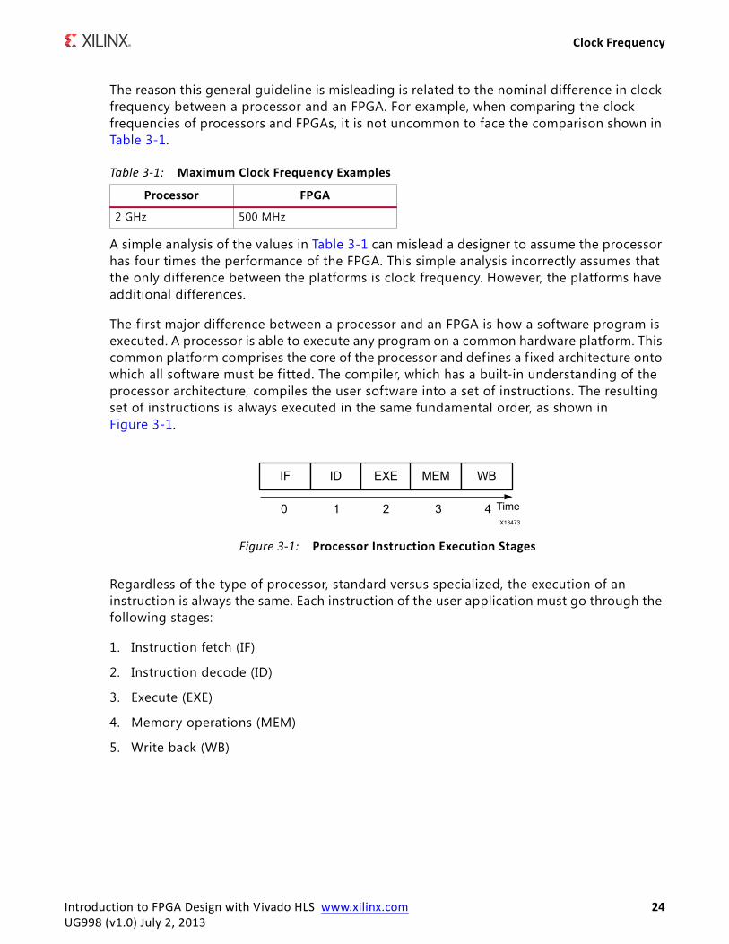
The first major difference between a processor and an FPGA is how a software program is executed. A processor is able to execute any program on a common hardware platform. This common platform comprises the core of the processor and defines a f ixed architecture onto which all software must be fitted. The compiler, which has a built-in understanding of the processor architecture, compiles the user software into a set of instructions. The resulting set of instructions is always executed in the same fundamental order, as shown in Figure 3-1.
Regardless of the type of processor, standard versus specialized, the execution of an instruction is always the same. Each instruction of the user application must go through the following stages:
1. Instruction fetch (IF)
2. Instruction decode (ID)
3. Execute (EXE)
4. Memory operations (MEM)
5. Write back (WB)
Table 3-1: Maximum Clock Frequency Examples
Processor FPGA
2 GHz 500 MHz
X-Ref Target - Figure 3-1
Figure 3-1: Processor Instruction Execution Stages
Introduction to FPGA Design with Vivado HLS www.xilinx.com 24UG998 (v1.0) July 2, 2013
Clock Frequency
The purpose of each stage is summarized in Table 3-2.
Most modern processors include multiple copies of the instruction execution path and are capable of running instructions with some degree of overlap. Because instructions in a processor usually depend on each other, the overlap between copies of the instruction execution hardware is not perfect. In the best of cases, only the overhead stages introduced by using a processor can be overlapped. The EXE stages, which are responsible for application computation, execute sequentially. The reasons for this sequential execution are related to limited resources in the EXE stage and dependence between instructions.
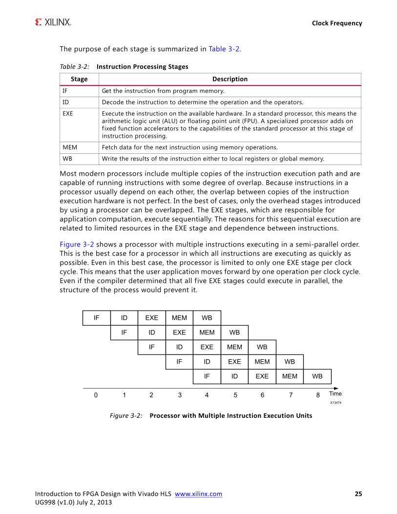
Figure 3-2 shows a processor with multiple instructions executing in a semi-parallel order. This is the best case for a processor in which all instructions are executing as quickly as possible. Even in this best case, the processor is limited to only one EXE stage per clock cycle. This means that the user application moves forward by one operation per clock cycle. Even if the compiler determined that all f ive EXE stages could execute in parallel, the structure of the process would prevent it.
Table 3-2: Instruction Processing Stages
Stage Description
IF Get the instruction from program memory.
ID Decode the instruction to determine the operation and the operators.
EXE Execute the instruction on the available hardware. In a standard processor, this means the arithmetic logic unit (ALU) or floating point unit (FPU). A specialized processor adds on f ixed function accelerators to the capabilities of the standard processor at this stage of instruction processing.
MEM Fetch data for the next instruction using memory operations.
WB Write the results of the instruction either to local registers or global memory.
X-Ref Target - Figure 3-2
Figure 3-2: Processor with Multiple Instruction Execution Units
Introduction to FPGA Design with Vivado HLS www.xilinx.com 25UG998 (v1.0) July 2, 2013
Clock Frequency
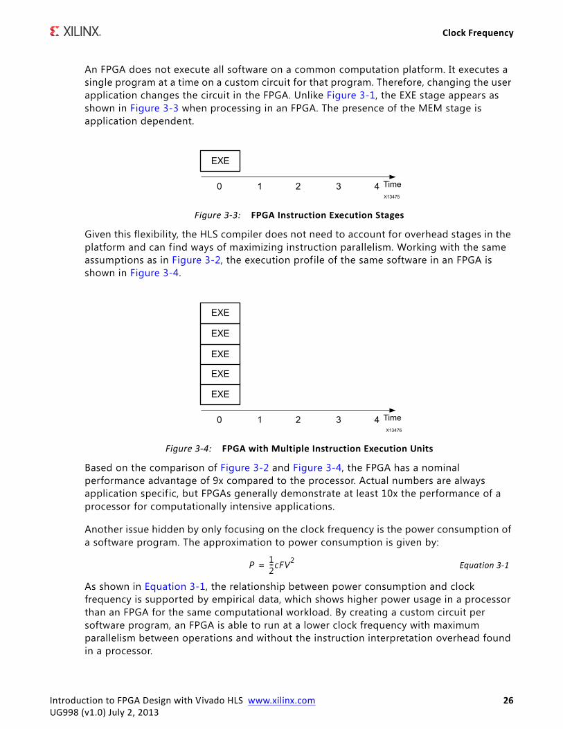
An FPGA does not execute all software on a common computation platform. It executes a single program at a time on a custom circuit for that program. Therefore, changing the user application changes the circuit in the FPGA. Unlike Figure 3-1, the EXE stage appears as shown in Figure 3-3 when processing in an FPGA. The presence of the MEM stage is application dependent.
Given this flexibility, the HLS compiler does not need to account for overhead stages in the platform and can f ind ways of maximizing instruction parallelism. Working with the same assumptions as in Figure 3-2, the execution profile of the same software in an FPGA is shown in Figure 3-4.
Based on the comparison of Figure 3-2 and Figure 3-4, the FPGA has a nominal performance advantage of 9x compared to the processor. Actual numbers are always application specific, but FPGAs generally demonstrate at least 10x the performance of a processor for computationally intensive applications.
Another issue hidden by only focusing on the clock frequency is the power consumption of a software program. The approximation to power consumption is given by:
Equation 3-1
As shown in Equation 3-1, the relationship between power consumption and clock frequency is supported by empirical data, which shows higher power usage in a processor than an FPGA for the same computational workload. By creating a custom circuit per software program, an FPGA is able to run at a lower clock frequency with maximum parallelism between operations and without the instruction interpretation overhead found in a processor.
X-Ref Target - Figure 3-3
Figure 3-3: FPGA Instruction Execution Stages
X-Ref Target - Figure 3-4
Figure 3-4: FPGA with Multiple Instruction Execution Units
P 12--cFV2
=
Introduction to FPGA Design with Vivado HLS www.xilinx.com 26UG998 (v1.0) July 2, 2013
Latency and Pipelining
RECOMMENDED: When selecting between a processor and an FPGA, it is recommended that application requirements and computational workload are analyzed based on throughput and latency instead of a maximum clock frequency.
Latency and PipeliningLatency is the number of clock cycles it takes to complete an instruction or set of instructions to generate an application result value. Using the basic processor architecture shown in Figure 3-1, the latency of an instruction is f ive clock cycles. If the application has a total of f ive instructions, the overall latency for this simple model is 25 clock cycles. That is, the result of the application is not available until 25 clock cycles expire.
Application latency is a key performance metric in both FPGAs and processors. In both cases, the problem of latency is resolved through the use of pipelining. In a processor, pipelining means that the next instruction can be launched into execution before the current instruction is complete. This allows the overlap of overhead stages required in instruction set processing. The best case result of pipelining for a processor is shown in Figure 3-2. By overlapping the execution of instructions, the processor achieves a latency of nine clock cycles for the five instruction application.
In an FPGA, the overhead cycles associated with instruction processing are not present. The latency is measured by how many clock cycles it takes to run the EXE stage of the original processor instruction. For the case in Figure 3-3, the latency is one clock cycle. Parallelism also plays an important role in latency. For the full f ive instruction application, the FPGA latency is also one clock cycle, as shown in Figure 3-4. With the one clock cycle latency of the FPGA, it might not be clear why pipelining is advantageous. However, the reason for pipelining in an FPGA is the same as in a processor, that is, to improve application performance.
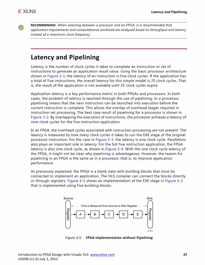
As previously explained, the FPGA is a blank slate with building blocks that must be connected to implement an application. The HLS compiler can connect the blocks directly or through registers. Figure 3-5 shows an implementation of the EXE stage in Figure 3-3 that is implemented using f ive building blocks.
X-Ref Target - Figure 3-5
Figure 3-5: FPGA Implementation without Pipelining
Introduction to FPGA Design with Vivado HLS www.xilinx.com 27UG998 (v1.0) July 2, 2013
Throughput
Operation timing in an FPGA is the length of time it takes a signal to travel from a source register to a sink register. Assuming each building block in Figure 3-5 requires 2 ns to execute, the current design requires 10 ns to implement the functionality. The latency is still one clock cycle, but the clock frequency is limited to 100 MHz. The 100 MHz frequency limit is derived from the definition of clock frequency in an FPGA. For the case of an FPGA circuit, the clock frequency is defined as the longest signal travel time between source and sink registers.
Pipelining in an FPGA is the process of inserting more registers to break up large computation blocks into smaller segments. This partitioning of the computation increases the latency in absolute number of clock cycles but increases performance by allowing the custom circuit to run at a higher clock frequency.
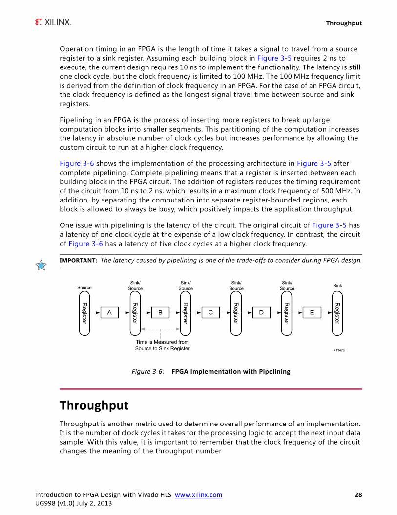
Figure 3-6 shows the implementation of the processing architecture in Figure 3-5 after complete pipelining. Complete pipelining means that a register is inserted between each building block in the FPGA circuit. The addition of registers reduces the timing requirement of the circuit from 10 ns to 2 ns, which results in a maximum clock frequency of 500 MHz. In addition, by separating the computation into separate register-bounded regions, each block is allowed to always be busy, which positively impacts the application throughput.
One issue with pipelining is the latency of the circuit. The original circuit of Figure 3-5 has a latency of one clock cycle at the expense of a low clock frequency. In contrast, the circuit of Figure 3-6 has a latency of f ive clock cycles at a higher clock frequency.
IMPORTANT: The latency caused by pipelining is one of the trade-offs to consider during FPGA design.
ThroughputThroughput is another metric used to determine overall performance of an implementation. It is the number of clock cycles it takes for the processing logic to accept the next input data sample. With this value, it is important to remember that the clock frequency of the circuit changes the meaning of the throughput number.
X-Ref Target - Figure 3-6
Figure 3-6: FPGA Implementation with Pipelining
Introduction to FPGA Design with Vivado HLS www.xilinx.com 28UG998 (v1.0) July 2, 2013
Memory Architecture and Layout
For example, both Figure 3-5 and Figure 3-6 show implementations that require one clock cycle between input data samples. The key difference is that the implementation in Figure 3-5 requires 10 ns between input samples, whereas the circuit in Figure 3-6 only requires 2 ns between input data samples. After the time base is known, it is clear that the second implementation has higher performance, because it can accept a higher input data rate.
Note: The definition of throughput described in this section can also be used when analyzing applications executing on a processor.
Memory Architecture and LayoutThe memory architecture of the selected implementation platform is one of the physical elements that can affect the performance of a software application. Memory architecture determines the upper bound on achievable performance. At some performance point, all applications on either a processor or an FPGA become memory bound regardless of the type and number of available computational resources. One strategy in FPGA design is understanding where the memory bound is and how it can be affected by data layout and memory organization.
In a processor-based system, the software engineer must f it the application on essentially the same memory architecture regardless of the specific type of processor. This commonality simplif ies the process of application migration at the expense of performance. Common memory architecture familiar to software engineers consists of memories that are slow, medium, or fast based on the number of clock cycles it takes to get the data to the processor. These memory classif ications are defined in Table 3-3.
The memory architecture shown in this table assumes that the user is presented with a single large memory space. Within this memory space, the user allocates and deallocates regions to store program data. The physical location of data and how it moves between the different levels in the hierarchy is handled by the computation platform and is transparent to the user. In this kind of system, the only way to boost performance is to reuse data in the cache as much as possible.
Table 3-3: Memory Type Definitions
Memory Type Definition
Slow Mass storage devices, such as hard drives
Medium DDR memories
Fast On-chip cache memories of different sizes depending on the specific processor
Introduction to FPGA Design with Vivado HLS www.xilinx.com 29UG998 (v1.0) July 2, 2013
Memory Architecture and Layout
To achieve this goal, the software engineer must spend large amounts of time looking at cache traces, restructuring the software algorithm to increase data locality, and managing memory allocation to minimize the instantaneous memory footprint of the program. Although all of these techniques are portable across processors, the results are not. A software program must be tuned for each processor it runs on to maximize performance.
With experience in working with processor-based memory, the first difference a software engineer encounters when working with memory in an FPGA is the lack of f ixed on-chip memory architecture. FPGA-based systems can be attached to slow and medium memories but exhibit the greatest degree of differentiation in terms of available fast memories. That is, instead of restructuring the software to best use an existing cache, the HLS compiler builds a fast memory architecture to best f it the data layout in the algorithm. The resulting FPGA implementation can have one or more internal banks of different sizes that can be accessed independently from one another.
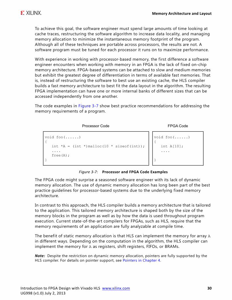
The code examples in Figure 3-7 show best practice recommendations for addressing the memory requirements of a program.
The FPGA code might surprise a seasoned software engineer with its lack of dynamic memory allocation. The use of dynamic memory allocation has long been part of the best practice guidelines for processor-based systems due to the underlying fixed memory architecture.
In contrast to this approach, the HLS compiler builds a memory architecture that is tailored to the application. This tailored memory architecture is shaped both by the size of the memory blocks in the program as well as by how the data is used throughout program execution. Current state-of-the-art compilers for FPGAs, such as HLS, require that the memory requirements of an application are fully analyzable at compile time.
The benefit of static memory allocation is that HLS can implement the memory for array A in different ways. Depending on the computation in the algorithm, the HLS compiler can implement the memory for A as registers, shift registers, FIFOs, or BRAMs.
Note: Despite the restriction on dynamic memory allocation, pointers are fully supported by the HLS compiler. For details on pointer support, see Pointers in Chapter 4.
X-Ref Target - Figure 3-7
Figure 3-7: Processor and FPGA Code Examples
Introduction to FPGA Design with Vivado HLS www.xilinx.com 30UG998 (v1.0) July 2, 2013
Memory Architecture and Layout
RegistersA register implementation of a memory is the fastest possible memory structure. In this implementation style, each entry of A becomes an independent entity. Each independent entity is embedded into the computation where it is used without the need to address logic or additional delays.
Shift RegisterIn processor programming terms, a shift register can be thought of as a special case of a queue. In this implementation, each element of A is used multiple times in different parts of the computation. The key characteristic of a shift register is that every element of A can be accessed on every clock cycle. In addition, moving all data items to the next adjacent storage container requires only one clock cycle.
FIFOA FIFO can be thought of as a queue with a single point of entry and a single point of exit. This kind of structure is typically used to transmit data between program loops or functions. There is no addressing logic involved, and the implementation details are completely handled by the HLS compiler.
BRAMA BRAM is a random-access memory that is embedded into the FPGA fabric. A Xilinx FPGA device includes many of these embedded memories. The exact number of memories is device specif ic. In processor programming terms, this kind of memory can be thought of as a cache with the following limitations:
• Does not implement cache coherency, collision, and cache miss tracking logic typically found in a processor cache.
• Holds its values only as long as the device is powered on.
• Supports parallel same cycle access to two different memory locations.
Introduction to FPGA Design with Vivado HLS www.xilinx.com 31UG998 (v1.0) July 2, 2013
Chapter 4
Vivado High-Level Synthesis
OverviewThe Xilinx® Vivado® High-Level Synthesis (HLS) compiler provides a programming environment similar to those available for application development on both standard and specialized processors. HLS shares key technology with processor compilers for the interpretation, analysis, and optimization of C/C++ programs. The main difference is in the execution target of the application.
By targeting an FPGA as the execution fabric, HLS enables a software engineer to optimize code for throughout, power, and latency without the need to address the performance bottleneck of a single memory space and limited computational resources. This allows the implementation of computationally intensive software algorithms into actual products, not just functionality demonstrators. This chapter introduces how the HLS compiler works and how it differs from a traditional software compiler.
Application code targeting the HLS compiler uses the same categories as any processor compiler. HLS analyzes all programs in terms of:
• Operations
• Conditional statements
• Loops
• Functions
IMPORTANT: HLS can compile almost any C/C++ program. The only coding limitation for HLS is with dynamic language constructs typical in processors with a single memory space. When using HLS, the main dynamic constructs to consider are memory allocation and pointers as described in this chapter.
OperationsOperations refer to both the arithmetic and logical components of an application that are involved in computing a result value. This definition intentionally excludes comparison statements, because these are handled in Conditional Statements.
Introduction to FPGA Design with Vivado HLS www.xilinx.com 32UG998 (v1.0) July 2, 2013
Operations
When working with operations, the main difference between HLS and other compilers is in the restrictions placed on the designer. With a processor compiler, the fixed processing architecture means that the user can only affect performance by limiting operation dependency and manipulating memory layout to maximize cache performance. In contrast, HLS is not constrained by a f ixed processing platform and builds an algorithm-specif ic platform based on user input. This allows an HLS designer to affect application performance in terms of throughput, latency, and power as shown in the examples in this section.
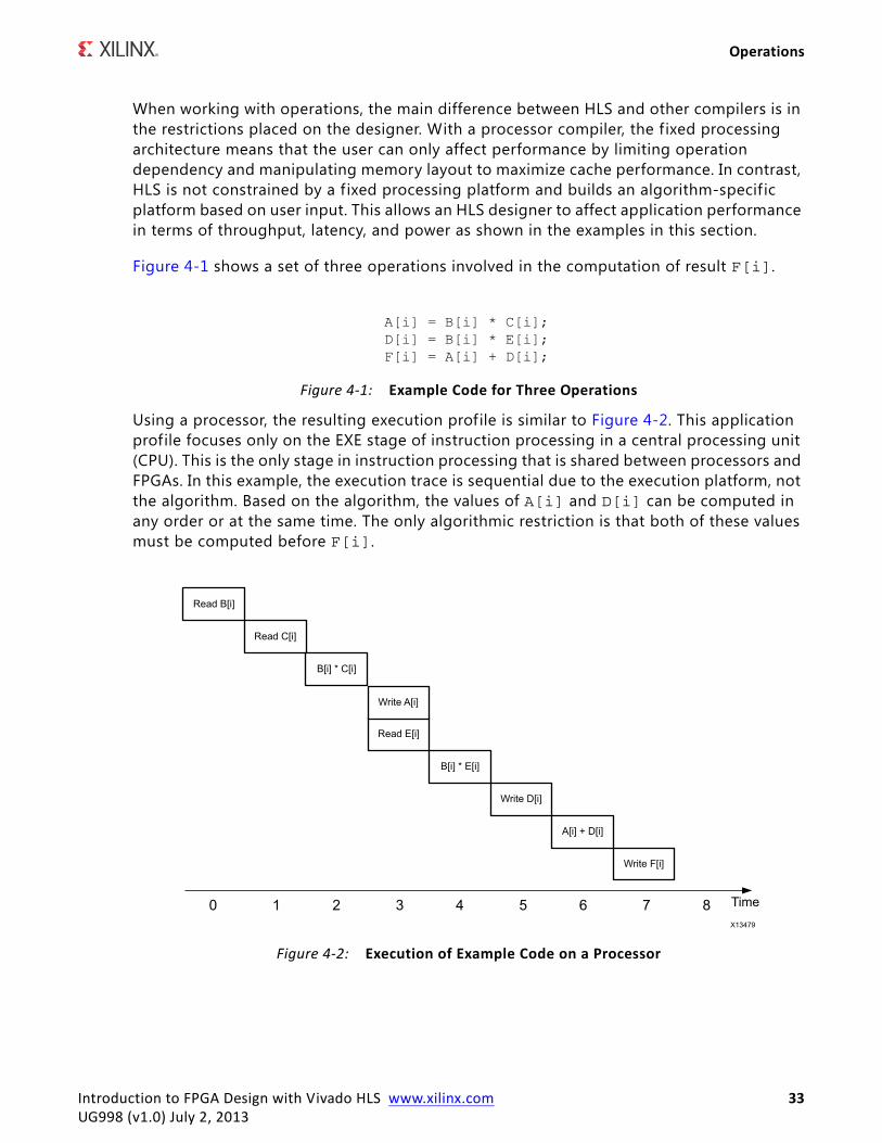
Figure 4-1 shows a set of three operations involved in the computation of result F[i].
Using a processor, the resulting execution profile is similar to Figure 4-2. This application profile focuses only on the EXE stage of instruction processing in a central processing unit (CPU). This is the only stage in instruction processing that is shared between processors and FPGAs. In this example, the execution trace is sequential due to the execution platform, not the algorithm. Based on the algorithm, the values of A[i] and D[i] can be computed in any order or at the same time. The only algorithmic restriction is that both of these values must be computed before F[i].
X-Ref Target - Figure 4-1
Figure 4-1: Example Code for Three Operations
X-Ref Target - Figure 4-2
Figure 4-2: Execution of Example Code on a Processor
Introduction to FPGA Design with Vivado HLS www.xilinx.com 33UG998 (v1.0) July 2, 2013
Operations
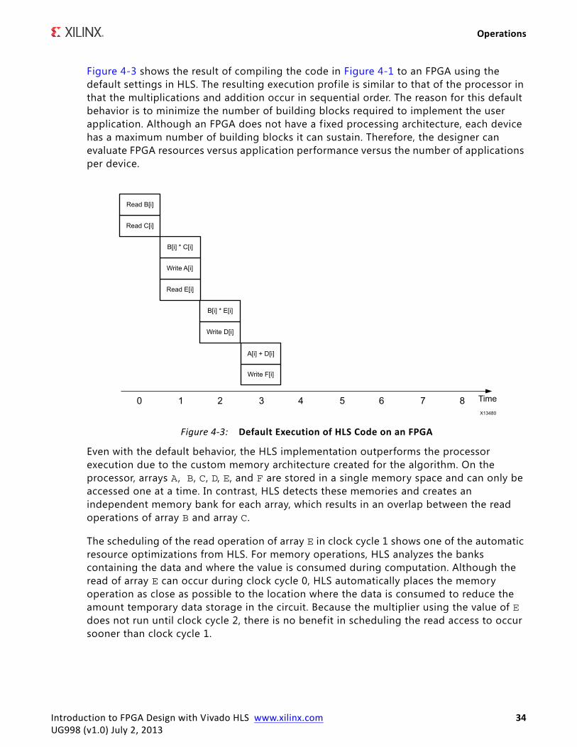
Figure 4-3 shows the result of compiling the code in Figure 4-1 to an FPGA using the default settings in HLS. The resulting execution profile is similar to that of the processor in that the multiplications and addition occur in sequential order. The reason for this default behavior is to minimize the number of building blocks required to implement the user application. Although an FPGA does not have a f ixed processing architecture, each device has a maximum number of building blocks it can sustain. Therefore, the designer can evaluate FPGA resources versus application performance versus the number of applications per device.
Even with the default behavior, the HLS implementation outperforms the processor execution due to the custom memory architecture created for the algorithm. On the processor, arrays A , B, C, D, E, and F are stored in a single memory space and can only be accessed one at a time. In contrast, HLS detects these memories and creates an independent memory bank for each array, which results in an overlap between the read operations of array B and array C.
The scheduling of the read operation of array E in clock cycle 1 shows one of the automatic resource optimizations from HLS. For memory operations, HLS analyzes the banks containing the data and where the value is consumed during computation. Although the read of array E can occur during clock cycle 0, HLS automatically places the memory operation as close as possible to the location where the data is consumed to reduce the amount temporary data storage in the circuit. Because the multiplier using the value of E does not run until clock cycle 2, there is no benefit in scheduling the read access to occur sooner than clock cycle 1.
X-Ref Target - Figure 4-3
Figure 4-3: Default Execution of HLS Code on an FPGA
Introduction to FPGA Design with Vivado HLS www.xilinx.com 34UG998 (v1.0) July 2, 2013
Conditional Statements
Another way in which HLS helps the user control the size of the generated circuit is by providing data types for the sizing of variables. Similar to all compilers, HLS offers the user access to integer, single precision, and double precision data types. This enables rapid migration of software onto the FPGA but might mask algorithm inefficiencies, which are a result of the 32-bit and 64-bit datapaths available in processors.
For example, assume that the code in Figure 4-1 only requires 20-bit values in arrays B, C, and E. In the original processor code, these bit sizes would require arrays A , D, and F to be capable of storing 64-bit values to avoid any loss of precision. HLS can compile the code as is, but this results in an ineff icient 64-bit datapath that consumes more resources than is required by the algorithm.
Figure 4-4 shows an example of how to rewrite the code in Figure 4-1 with the HLS arbitrary precision data types. The use of these data types enables rapid software-level exploration and validation of the minimum required precision needed for algorithm correctness. Besides reducing the number of resources required to implement a computation, the use of arbitrary precision data types reduces the number of levels of logic required to complete an operation. This in turn reduces the latency of a design.
As mentioned in Chapter 3, Basic Concepts of Hardware Design, pipelining, or the division of computation into smaller register-bound regions, is an essential FPGA design technique for achieving a target clock frequency. Based on the size of operations, this optimization is automatically implemented by HLS. HLS divides large operators into multiple computation stages with a corresponding increase in circuit latency.
Conditional StatementsConditional statements are program control flow statements that are typically implemented as if, if-else, or case statements. These coding structures are an integral part of most algorithms and are fully supported by all compilers, including HLS. The only difference between compilers is how these types of statements are implemented.
X-Ref Target - Figure 4-4
Figure 4-4: Coding Example Using HLS Arbitrary Precision Types
Introduction to FPGA Design with Vivado HLS www.xilinx.com 35UG998 (v1.0) July 2, 2013
Loops
With a processor compiler, conditional statements are translated into branch operations that might or might not result in a context switch. The introduction of branches disrupts the maximum instruction execution packing shown in Figure 3-2 by introducing a dependence that affects which instruction is fetched next from memory. This uncertainty results in bubbles in the processor execution pipeline and directly affects program performance.
In an FPGA, a conditional statement does not have the same potential impact on performance as in a processor. HLS creates all the circuits described by each branch of the conditional statement. Therefore, the runtime execution of a conditional software statement involves the selection between two possible results rather than a context switch.
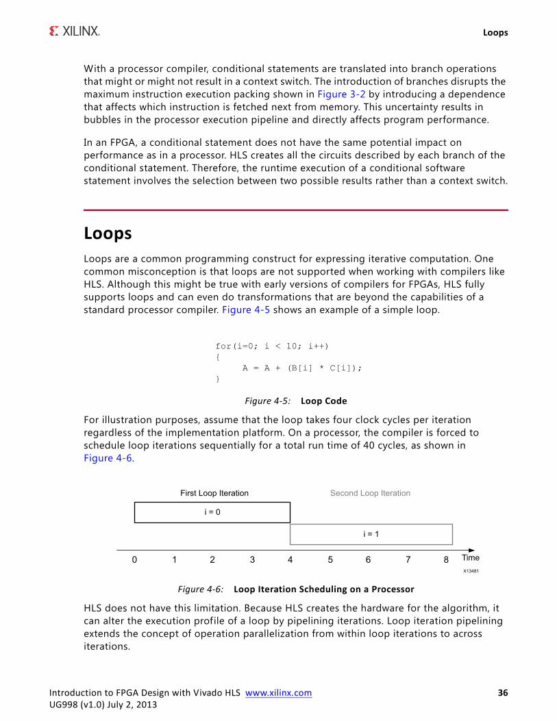
LoopsLoops are a common programming construct for expressing iterative computation. One common misconception is that loops are not supported when working with compilers like HLS. Although this might be true with early versions of compilers for FPGAs, HLS fully supports loops and can even do transformations that are beyond the capabilities of a standard processor compiler. Figure 4-5 shows an example of a simple loop.
For illustration purposes, assume that the loop takes four clock cycles per iteration regardless of the implementation platform. On a processor, the compiler is forced to schedule loop iterations sequentially for a total run time of 40 cycles, as shown in Figure 4-6.
HLS does not have this limitation. Because HLS creates the hardware for the algorithm, it can alter the execution profile of a loop by pipelining iterations. Loop iteration pipelining extends the concept of operation parallelization from within loop iterations to across iterations.
X-Ref Target - Figure 4-5
Figure 4-5: Loop Code
X-Ref Target - Figure 4-6
Figure 4-6: Loop Iteration Scheduling on a Processor
Introduction to FPGA Design with Vivado HLS www.xilinx.com 36UG998 (v1.0) July 2, 2013
Loops
To reduce iteration latency, the first automatic optimization applied by HLS is operator parallelization to the loop iteration body. The second optimization is loop iteration pipelining. This optimization requires user input, because it affects the resource consumption and input data rates of the FPGA implementation.
The default behavior of HLS is to execute loops in the same schedule as a processor, as shown in Figure 4-6. This means that the code in Figure 4-5 has a processing latency of 40 cycles and an input data rate of once every 4 cycles. In this example, the input data rate is defined by how quickly the values of B and C can be sampled from the input.
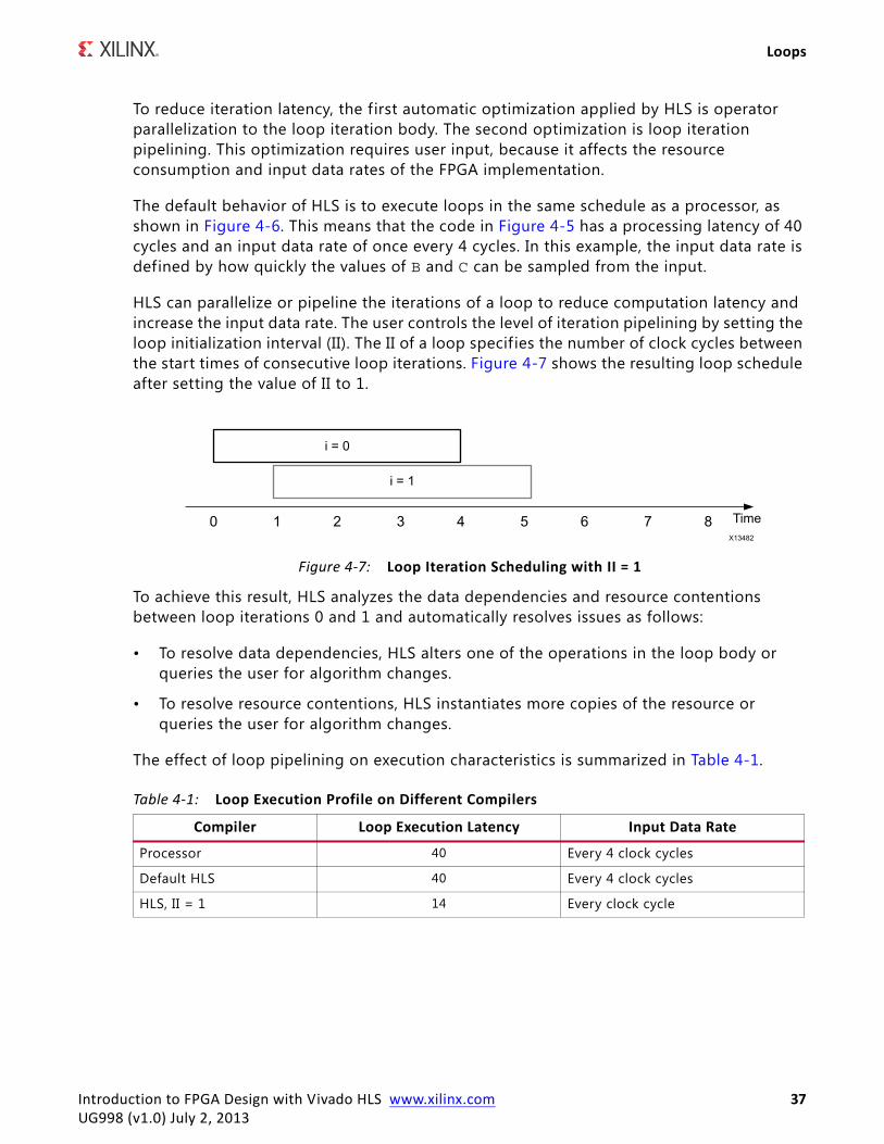
HLS can parallelize or pipeline the iterations of a loop to reduce computation latency and increase the input data rate. The user controls the level of iteration pipelining by setting the loop initialization interval (II). The II of a loop specif ies the number of clock cycles between the start times of consecutive loop iterations. Figure 4-7 shows the resulting loop schedule after setting the value of II to 1.
To achieve this result, HLS analyzes the data dependencies and resource contentions between loop iterations 0 and 1 and automatically resolves issues as follows:
• To resolve data dependencies, HLS alters one of the operations in the loop body or queries the user for algorithm changes.
• To resolve resource contentions, HLS instantiates more copies of the resource or queries the user for algorithm changes.
The effect of loop pipelining on execution characteristics is summarized in Table 4-1.
X-Ref Target - Figure 4-7
Figure 4-7: Loop Iteration Scheduling with II = 1
Table 4-1: Loop Execution Profile on Different Compilers
Compiler Loop Execution Latency Input Data Rate
Processor 40 Every 4 clock cycles
Default HLS 40 Every 4 clock cycles
HLS, II = 1 14 Every clock cycle
Introduction to FPGA Design with Vivado HLS www.xilinx.com 37UG998 (v1.0) July 2, 2013
Functions
FunctionsFunctions are a programming hierarchy that can contain operators, loops, and other functions. The treatment of functions in both HLS and processor compilers is similar to that of loops.
In HLS, the main difference between loops and functions is related to terminology. HLS can parallelize the execution of both loops and functions. With loops, this transformation is typically referred to as pipelining, because there is a clear hierarchy difference between operators and loop iterations. With functions, operations outside of a loop body and within loops are in the same hierarchical context, which might lead to confusion if the term pipelining is used. To avoid potential confusion when working with HLS, the parallelization of function call execution is referred to as dataflow optimization.
The dataflow optimization instructs HLS to create independent hardware modules for all functions at a given level of program hierarchy. These independent hardware modules are capable of concurrent execution and self-synchronize during data transfer.
Dynamic Memory AllocationDynamic memory allocation is one of the memory management techniques available in the C and C++ programming languages. In this method, the user can allocate as much memory as necessary during program runtime. The size of the allocated memory can vary between executions of the program and is allocated from a central physical pool of memory as described in Chapter 3, Basic Concepts of Hardware Design. The function calls typically associated with dynamic memory allocation are shown in Table 4-2.
As discussed in Chapter 3, Basic Concepts of Hardware Design, an FPGA does not have a f ixed memory architecture onto which the HLS compiler must f it the user application. Instead, HLS synthesizes the memory architecture based on the unique requirements of the algorithm. Therefore, all code provided to the HLS compiler for implementation in an FPGA must use compile time analyzable memory allocation only.
Table 4-2: Functions Used in Dynamic Memory Management
C C++
malloc() new()
calloc() delete()
free()
Introduction to FPGA Design with Vivado HLS www.xilinx.com 38UG998 (v1.0) July 2, 2013
Dynamic Memory Allocation
To aid the user in ensuring that all code provided to HLS is synthesizable, the compiler executes a coding compliance pass before analyzing the design. This code compliance pass flags all coding styles that are not suitable for HLS. It is the responsibility of the user to manually change the code and remove all instances of dynamic memory allocation.
The code in Figure 4-8 allocates a region in memory to store 10 values of 32 bits each.
Although this coding example clearly states a constant memory allocation, the HLS code compliance stage does not analyze the contents of the malloc statement. HLS cannot synthesize code that includes any of the keywords in Table 4-2 even if the allocation is constant, as in the example shown in Figure 4-8. There are two possible methods of modifying this code to comply with HLS. The following code examples show these methods and explain their implications on the FPGA implementation.
The code in Figure 4-9 shows automatic memory allocation by a C/C++ program. HLS implements this memory style in strict accordance with the behavior stipulated by C/C++. This means that the memory created to store array A only stores valid data values during the duration of the function call containing this array. Therefore, the function call is responsible for populating A with valid data before each use.
The code in Figure 4-10 shows static memory allocation by a C/C++ program. The behavior for this type of memory allocation dictates that the contents of array A are valid across function calls until the program is completely shut down. When working with HLS, the memory that is implemented for array A contains valid data as long as there is power to the circuit.
Both automatic and static memory allocation techniques can increase the overall software memory footprint of an algorithm running on a processor. When specifying algorithms in C/C++ for FPGA implementation, the most important consideration is the overall goal of the user application. That is, the main goal when compiling to an FPGA is not creating the best software algorithm implementation. Instead, when using tools like HLS, the goal is to capture the algorithm in a way that allows the tool to infer the best possible hardware architecture, which results in the best possible implementation.
X-Ref Target - Figure 4-8
Figure 4-8: Dynamic Memory Allocation
X-Ref Target - Figure 4-9
Figure 4-9: HLS-Compliant Automatic Memory Allocation
X-Ref Target - Figure 4-10
Figure 4-10: HLS-Compliant Static Memory Allocation
Introduction to FPGA Design with Vivado HLS www.xilinx.com 39UG998 (v1.0) July 2, 2013
Pointers
PointersA pointer is an address to a location in memory. Some of the common uses for pointers in a C/C++ program are function parameters, array handling, pointer to pointer, and type casting. The inherent flexibility of this language construct makes it a useful and popular element of C/C++ code. The HLS compiler supports pointer usage that can be completely analyzed at compile time. An analyzable pointer usage is usage that can be fully expressed and computed in a pen and paper computation without the need for runtime information.
The code in Figure 4-8 shows the use of a pointer to reference a dynamically allocated region in memory. As previously described, this usage is not supported with HLS, because the destination address of the pointer is only known during program execution. This does not mean that pointer usage for memory management is unsupported when using the HLS compiler. Figure 4-11 shows a valid coding style in which pointers are used to access a memory.
This code is valid, because all uses of pointer pA can be analyzed and mapped back to array A. Because array A is created by automatic memory allocation, HLS can fully determine the properties of A.
Another supported model for memories and pointers is in accessing external memory. When using HLS, any pointer access on function parameters implies either a variable or an external memory. HLS defines an external memory as any memory outside of the scope of the compiler-generated RTL. This means that the memory might be located in another function in the FPGA or in part of an off-chip memory, such as DDR.
X-Ref Target - Figure 4-11
Figure 4-11: Managing Array Access with a Pointer
Introduction to FPGA Design with Vivado HLS www.xilinx.com 40UG998 (v1.0) July 2, 2013
Pointers
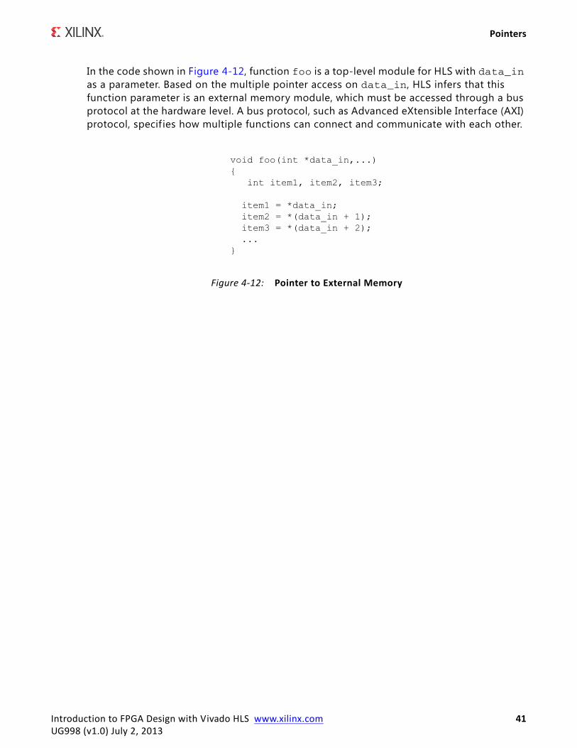
In the code shown in Figure 4-12, function foo is a top-level module for HLS with data_in as a parameter. Based on the multiple pointer access on data_in, HLS infers that this function parameter is an external memory module, which must be accessed through a bus protocol at the hardware level. A bus protocol, such as Advanced eXtensible Interface (AXI) protocol, specif ies how multiple functions can connect and communicate with each other.
X-Ref Target - Figure 4-12
Figure 4-12: Pointer to External Memory
Introduction to FPGA Design with Vivado HLS www.xilinx.com 41UG998 (v1.0) July 2, 2013
Chapter 5
Computation-Centric Algorithms
OverviewAlthough there is a large body of literature on algorithm analysis, the nuances of computation- versus control-centric algorithms are largely dependent on the implementation platform. This chapter defines computation-centric algorithms in the context of the Vivado® HLS compiler and FPGAs. It also includes examples and best practice recommendations to maximize the performance of the HLS-generated implementation.
A computation-centric algorithm is an algorithm that is configured once per task and cannot change its behavior for the duration of a task. A task in hardware is the same as a function call in a C/C++ program. The size of the task is under the control of the HLS user.
RECOMMENDED: In general, it is recommended that the size of a task be based on the natural work division in the algorithm.
Figure 5-1 shows the code for a Sobel edge detection operation. This is an example of a computation-centric algorithm that can be divided into tasks of different sizes. This algorithm is a two-dimensional f iltering operation that computes the edge of a region in an image by computing the gradient of each pixel in the x and y directions. As currently written, this code can be compiled by HLS into an FPGA implementation.
X-Ref Target - Figure 5-1
Figure 5-1: Sobel Edge Detection Algorithm—Task Choice 1
Introduction to FPGA Design with Vivado HLS www.xilinx.com 42UG998 (v1.0) July 2, 2013
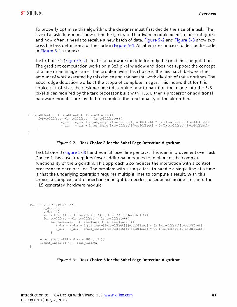
Overview
To properly optimize this algorithm, the designer must f irst decide the size of a task. The size of a task determines how often the generated hardware module needs to be configured and how often it needs to receive a new batch of data. Figure 5-2 and Figure 5-3 show two possible task definitions for the code in Figure 5-1. An alternate choice is to define the code in Figure 5-1 as a task.
Task Choice 2 (Figure 5-2) creates a hardware module for only the gradient computation. The gradient computation works on a 3x3 pixel window and does not support the concept of a line or an image frame. The problem with this choice is the mismatch between the amount of work executed by this choice and the natural work division of the algorithm. The Sobel edge detection works at the scope of complete images. This means that for this choice of task size, the designer must determine how to partition the image into the 3x3 pixel slices required by the task processor built with HLS. Either a processor or additional hardware modules are needed to complete the functionality of the algorithm.
Task Choice 3 (Figure 5-3) handles a full pixel line per task. This is an improvement over Task Choice 1, because it requires fewer additional modules to implement the complete functionality of the algorithm. This approach also reduces the interaction with a control processor to once per line. The problem with sizing a task to handle a single line at a time is that the underlying operation requires multiple lines to compute a result. With this choice, a complex control mechanism might be needed to sequence image lines into the HLS-generated hardware module.
X-Ref Target - Figure 5-2
Figure 5-2: Task Choice 2 for the Sobel Edge Detection Algorithm
X-Ref Target - Figure 5-3
Figure 5-3: Task Choice 3 for the Sobel Edge Detection Algorithm
Introduction to FPGA Design with Vivado HLS www.xilinx.com 43UG998 (v1.0) July 2, 2013
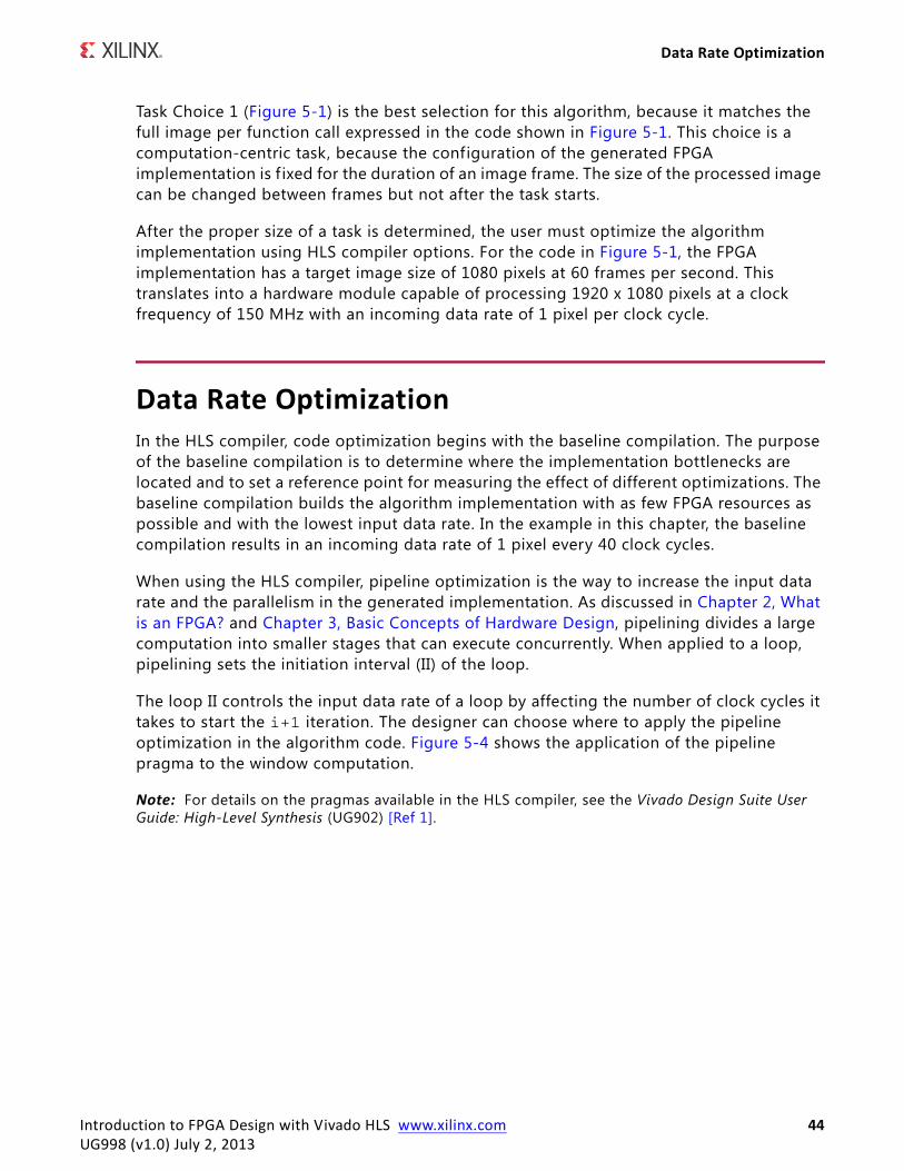
Data Rate Optimization
Task Choice 1 (Figure 5-1) is the best selection for this algorithm, because it matches the full image per function call expressed in the code shown in Figure 5-1. This choice is a computation-centric task, because the configuration of the generated FPGA implementation is f ixed for the duration of an image frame. The size of the processed image can be changed between frames but not after the task starts.
After the proper size of a task is determined, the user must optimize the algorithm implementation using HLS compiler options. For the code in Figure 5-1, the FPGA implementation has a target image size of 1080 pixels at 60 frames per second. This translates into a hardware module capable of processing 1920 x 1080 pixels at a clock frequency of 150 MHz with an incoming data rate of 1 pixel per clock cycle.
Data Rate OptimizationIn the HLS compiler, code optimization begins with the baseline compilation. The purpose of the baseline compilation is to determine where the implementation bottlenecks are located and to set a reference point for measuring the effect of different optimizations. The baseline compilation builds the algorithm implementation with as few FPGA resources as possible and with the lowest input data rate. In the example in this chapter, the baseline compilation results in an incoming data rate of 1 pixel every 40 clock cycles.
When using the HLS compiler, pipeline optimization is the way to increase the input data rate and the parallelism in the generated implementation. As discussed in Chapter 2, What is an FPGA? and Chapter 3, Basic Concepts of Hardware Design, pipelining divides a large computation into smaller stages that can execute concurrently. When applied to a loop, pipelining sets the initiation interval (II) of the loop.
The loop II controls the input data rate of a loop by affecting the number of clock cycles it takes to start the i+1 iteration. The designer can choose where to apply the pipeline optimization in the algorithm code. Figure 5-4 shows the application of the pipeline pragma to the window computation.
Note: For details on the pragmas available in the HLS compiler, see the Vivado Design Suite User Guide: High-Level Synthesis (UG902) [Ref 1].
Introduction to FPGA Design with Vivado HLS www.xilinx.com 44UG998 (v1.0) July 2, 2013
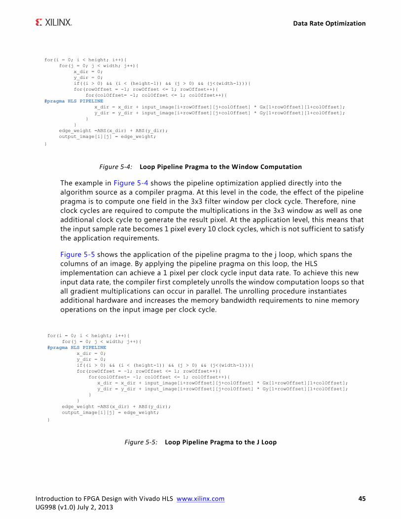
Data Rate Optimization
The example in Figure 5-4 shows the pipeline optimization applied directly into the algorithm source as a compiler pragma. At this level in the code, the effect of the pipeline pragma is to compute one field in the 3x3 f ilter window per clock cycle. Therefore, nine clock cycles are required to compute the multiplications in the 3x3 window as well as one additional clock cycle to generate the result pixel. At the application level, this means that the input sample rate becomes 1 pixel every 10 clock cycles, which is not suff icient to satisfy the application requirements.
Figure 5-5 shows the application of the pipeline pragma to the j loop, which spans the columns of an image. By applying the pipeline pragma on this loop, the HLS implementation can achieve a 1 pixel per clock cycle input data rate. To achieve this new input data rate, the compiler f irst completely unrolls the window computation loops so that all gradient multiplications can occur in parallel. The unrolling procedure instantiates additional hardware and increases the memory bandwidth requirements to nine memory operations on the input image per clock cycle.
X-Ref Target - Figure 5-4
Figure 5-4: Loop Pipeline Pragma to the Window Computation
X-Ref Target - Figure 5-5
Figure 5-5: Loop Pipeline Pragma to the J Loop
Introduction to FPGA Design with Vivado HLS www.xilinx.com 45UG998 (v1.0) July 2, 2013
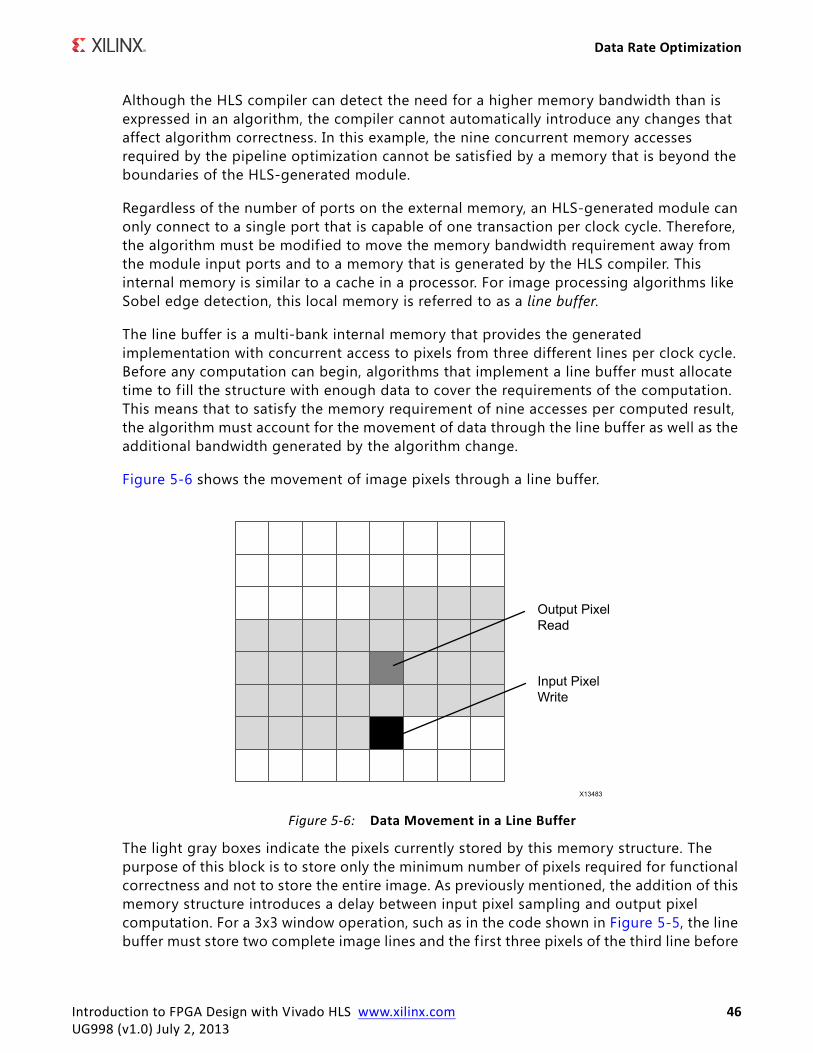
Data Rate Optimization
Although the HLS compiler can detect the need for a higher memory bandwidth than is expressed in an algorithm, the compiler cannot automatically introduce any changes that affect algorithm correctness. In this example, the nine concurrent memory accesses required by the pipeline optimization cannot be satisfied by a memory that is beyond the boundaries of the HLS-generated module.
Regardless of the number of ports on the external memory, an HLS-generated module can only connect to a single port that is capable of one transaction per clock cycle. Therefore, the algorithm must be modif ied to move the memory bandwidth requirement away from the module input ports and to a memory that is generated by the HLS compiler. This internal memory is similar to a cache in a processor. For image processing algorithms like Sobel edge detection, this local memory is referred to as a line buffer.
The line buffer is a multi-bank internal memory that provides the generated implementation with concurrent access to pixels from three different lines per clock cycle. Before any computation can begin, algorithms that implement a line buffer must allocate time to f ill the structure with enough data to cover the requirements of the computation. This means that to satisfy the memory requirement of nine accesses per computed result, the algorithm must account for the movement of data through the line buffer as well as the additional bandwidth generated by the algorithm change.
Figure 5-6 shows the movement of image pixels through a line buffer.
The light gray boxes indicate the pixels currently stored by this memory structure. The purpose of this block is to store only the minimum number of pixels required for functional correctness and not to store the entire image. As previously mentioned, the addition of this memory structure introduces a delay between input pixel sampling and output pixel computation. For a 3x3 window operation, such as in the code shown in Figure 5-5, the line buffer must store two complete image lines and the f irst three pixels of the third line before
X-Ref Target - Figure 5-6
Figure 5-6: Data Movement in a Line Buffer
Introduction to FPGA Design with Vivado HLS www.xilinx.com 46UG998 (v1.0) July 2, 2013
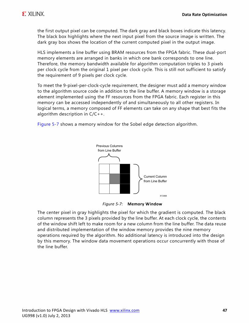
Data Rate Optimization
the f irst output pixel can be computed. The dark gray and black boxes indicate this latency. The black box highlights where the next input pixel from the source image is written. The dark gray box shows the location of the current computed pixel in the output image.
HLS implements a line buffer using BRAM resources from the FPGA fabric. These dual-port memory elements are arranged in banks in which one bank corresponds to one line. Therefore, the memory bandwidth available for algorithm computation triples to 3 pixels per clock cycle from the original 1 pixel per clock cycle. This is still not suff icient to satisfy the requirement of 9 pixels per clock cycle.
To meet the 9-pixel-per-clock-cycle requirement, the designer must add a memory window to the algorithm source code in addition to the line buffer. A memory window is a storage element implemented using the FF resources from the FPGA fabric. Each register in this memory can be accessed independently of and simultaneously to all other registers. In logical terms, a memory composed of FF elements can take on any shape that best f its the algorithm description in C/C++.
Figure 5-7 shows a memory window for the Sobel edge detection algorithm.
The center pixel in gray highlights the pixel for which the gradient is computed. The black column represents the 3 pixels provided by the line buffer. At each clock cycle, the contents of the window shift left to make room for a new column from the line buffer. The data reuse and distributed implementation of the window memory provides the nine memory operations required by the algorithm. No additional latency is introduced into the design by this memory. The window data movement operations occur concurrently with those of the line buffer.
X-Ref Target - Figure 5-7
Figure 5-7: Memory Window
Introduction to FPGA Design with Vivado HLS www.xilinx.com 47UG998 (v1.0) July 2, 2013
Data Rate Optimization
The overall data movement from input to computation through a tiered memory architecture is shown in Figure 5-8.
Figure 5-9 shows the algorithm code changes required to implement the tiered memory architecture. This tiered architecture allows the HLS-generated implementation to achieve a 1-pixel-per-clock-cycle input data rate. In this code example, the computation kernel of the algorithm is in the sobel_operator function. The main change in this code is the extension of the rows and columns loops by one iteration each. This extension accounts for the additional task execution time introduced by the line buffer. In addition, the write operations into the line buffer are guarded by if conditions that are based on the original image boundaries. The algorithm output write operations are based on the output image positioning, which is offset by 1 row and 1 column from the original image.
As shown in Figure 5-9, a computation-centric application can have embedded control statements in the form of for-loops, if-else statements, and so forth. The key characteristic of this kind of algorithm is that its function and behavior are f ixed for the duration of a task. The HLS-generated module processes a batch of data based on a given configuration. The configuration can change between every task, but never during a task.
TIP: Line buffer manipulation libraries are part of the video libraries available with the HLS compiler. For more information, see the Vivado Design Suite User Guide: High-Level Synthesis (UG902) [Ref 1].
X-Ref Target - Figure 5-8
Figure 5-8: Data Movement from Input to Computation
Introduction to FPGA Design with Vivado HLS www.xilinx.com 48UG998 (v1.0) July 2, 2013
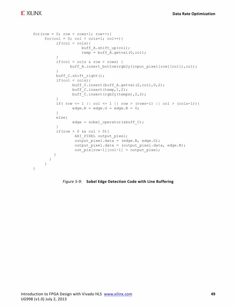
Data Rate Optimization
X-Ref Target - Figure 5-9
Figure 5-9: Sobel Edge Detection Code with Line Buffering
Introduction to FPGA Design with Vivado HLS www.xilinx.com 49UG998 (v1.0) July 2, 2013
Chapter 6
Control-Centric Algorithms
OverviewA control-centric algorithm is an algorithm that can be changed during task execution based on system-level factors. Whereas a computation-centric algorithm applies the same operations to all input data values for the duration of a task, a control-centric algorithm determines its operation based on the current input port status. This chapter describes the best practices for optimizing these types of applications with the Vivado® HLS compiler.
Expressing Control in C/C++Before describing best practices, it is important to review how control is expressed in the C and C++ languages.
LoopsLoops are a fundamental programming construct for expressing iterative computation. Like all compilers, HLS allows loops to be expressed as for-loops, while-loops, and do-while loops. This construct is supported in all types of applications compiled with HLS. As demonstrated in the Sobel edge detection example in Chapter 5, Computation-Centric Algorithms, loops are essential to the capture of computation-intensive algorithms in C/C++.
Introduction to FPGA Design with Vivado HLS www.xilinx.com 50UG998 (v1.0) July 2, 2013
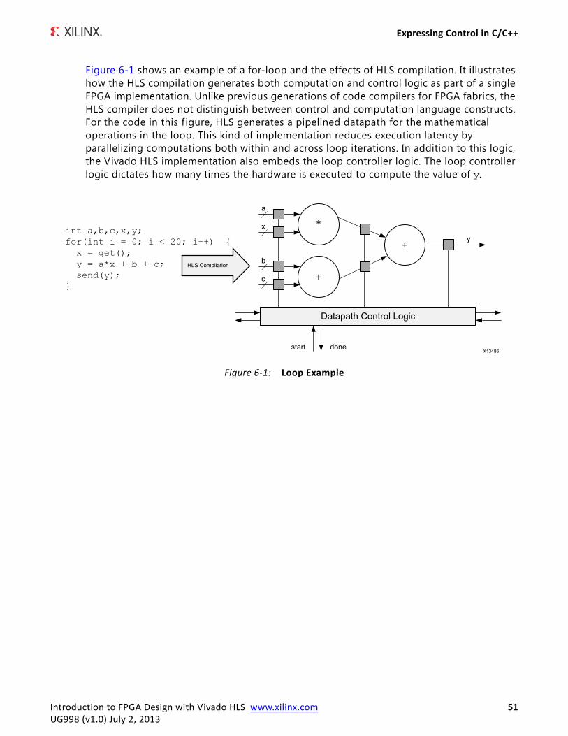
Expressing Control in C/C++
Figure 6-1 shows an example of a for-loop and the effects of HLS compilation. It illustrates how the HLS compilation generates both computation and control logic as part of a single FPGA implementation. Unlike previous generations of code compilers for FPGA fabrics, the HLS compiler does not distinguish between control and computation language constructs. For the code in this f igure, HLS generates a pipelined datapath for the mathematical operations in the loop. This kind of implementation reduces execution latency by parallelizing computations both within and across loop iterations. In addition to this logic, the Vivado HLS implementation also embeds the loop controller logic. The loop controller logic dictates how many times the hardware is executed to compute the value of y.
X-Ref Target - Figure 6-1
Figure 6-1: Loop Example
Introduction to FPGA Design with Vivado HLS www.xilinx.com 51UG998 (v1.0) July 2, 2013
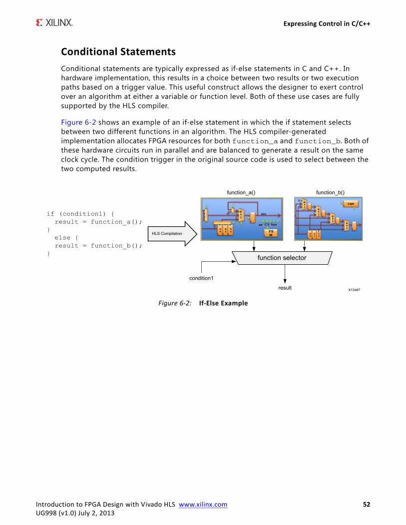
Expressing Control in C/C++
Conditional StatementsConditional statements are typically expressed as if-else statements in C and C++. In hardware implementation, this results in a choice between two results or two execution paths based on a trigger value. This useful construct allows the designer to exert control over an algorithm at either a variable or function level. Both of these use cases are fully supported by the HLS compiler.
Figure 6-2 shows an example of an if-else statement in which the if statement selects between two different functions in an algorithm. The HLS compiler-generated implementation allocates FPGA resources for both function_a and function_b. Both of these hardware circuits run in parallel and are balanced to generate a result on the same clock cycle. The condition trigger in the original source code is used to select between the two computed results.
X-Ref Target - Figure 6-2
Figure 6-2: If-Else Example
Introduction to FPGA Design with Vivado HLS www.xilinx.com 52UG998 (v1.0) July 2, 2013
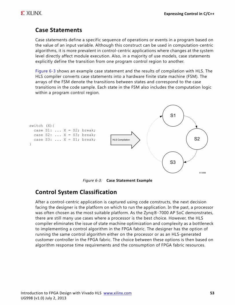
Expressing Control in C/C++
Case StatementsCase statements define a specific sequence of operations or events in a program based on the value of an input variable. Although this construct can be used in computation-centric algorithms, it is more prevalent in control-centric applications where changes at the system level directly affect module execution. Also, in a majority of use models, case statements explicitly define the transition from one program control region to another.
Figure 6-3 shows an example case statement and the results of compilation with HLS. The HLS compiler converts case statements into a hardware finite state machine (FSM). The arrays of the FSM denote the transitions between states and correspond to the case transitions in the code sample. Each state in the FSM also includes the computation logic within a program control region.
Control System ClassificationAfter a control-centric application is captured using code constructs, the next decision facing the designer is the platform on which to run the application. In the past, a processor was often chosen as the most suitable platform. As the Zynq®-7000 AP SoC demonstrates, there are still many use cases where a processor is the best choice. However, the HLS compiler eliminates the issue of state machine optimization and complexity as a bottleneck to implementing a control algorithm in the FPGA fabric. The designer has the option of running the same control algorithm either on the processor or as an HLS-generated customer controller in the FPGA fabric. The choice between these options is then based on algorithm response time requirements and the consumption of FPGA fabric resources.
X-Ref Target - Figure 6-3
Figure 6-3: Case Statement Example
Introduction to FPGA Design with Vivado HLS www.xilinx.com 53UG998 (v1.0) July 2, 2013
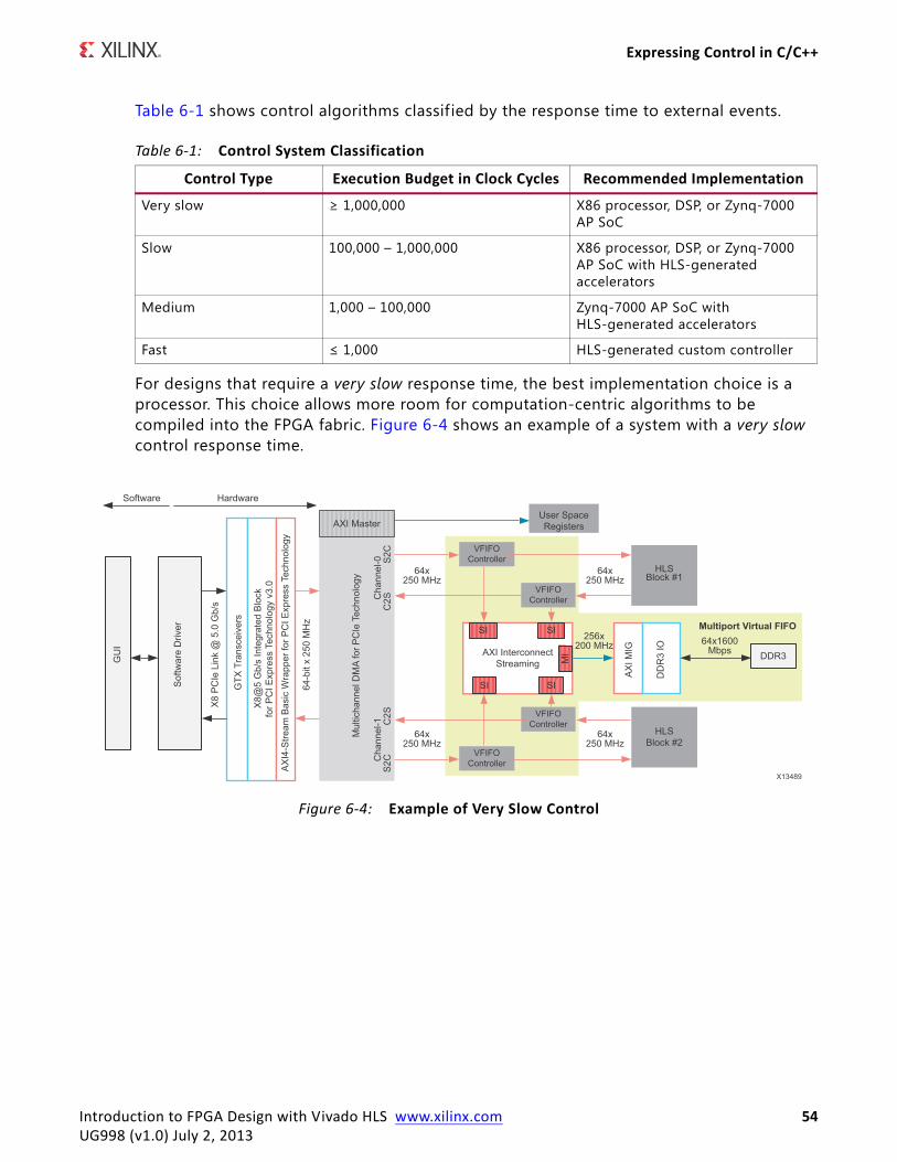
Expressing Control in C/C++
Table 6-1 shows control algorithms classif ied by the response time to external events.
For designs that require a very slow response time, the best implementation choice is a processor. This choice allows more room for computation-centric algorithms to be compiled into the FPGA fabric. Figure 6-4 shows an example of a system with a very slow control response time.
Table 6-1: Control System Classification
Control Type Execution Budget in Clock Cycles Recommended Implementation
Very slow ≥ 1,000,000 X86 processor, DSP, or Zynq-7000 AP SoC
Slow 100,000 – 1,000,000 X86 processor, DSP, or Zynq-7000 AP SoC with HLS-generated accelerators
Medium 1,000 – 100,000 Zynq-7000 AP SoC with HLS-generated accelerators
Fast ≤ 1,000 HLS-generated custom controller
X-Ref Target - Figure 6-4
Figure 6-4: Example of Very Slow Control
Introduction to FPGA Design with Vivado HLS www.xilinx.com 54UG998 (v1.0) July 2, 2013
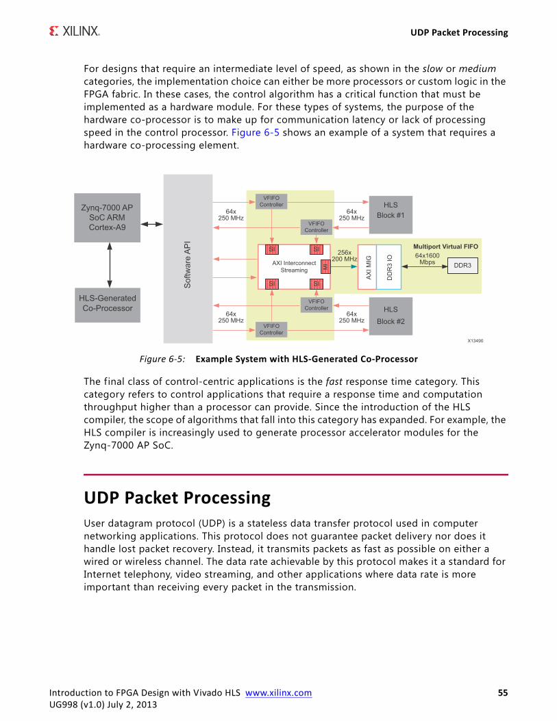
UDP Packet Processing
For designs that require an intermediate level of speed, as shown in the slow or medium categories, the implementation choice can either be more processors or custom logic in the FPGA fabric. In these cases, the control algorithm has a critical function that must be implemented as a hardware module. For these types of systems, the purpose of the hardware co-processor is to make up for communication latency or lack of processing speed in the control processor. Figure 6-5 shows an example of a system that requires a hardware co-processing element.
The final class of control-centric applications is the fast response time category. This category refers to control applications that require a response time and computation throughput higher than a processor can provide. Since the introduction of the HLS compiler, the scope of algorithms that fall into this category has expanded. For example, the HLS compiler is increasingly used to generate processor accelerator modules for the Zynq-7000 AP SoC.
UDP Packet ProcessingUser datagram protocol (UDP) is a stateless data transfer protocol used in computer networking applications. This protocol does not guarantee packet delivery nor does it handle lost packet recovery. Instead, it transmits packets as fast as possible on either a wired or wireless channel. The data rate achievable by this protocol makes it a standard for Internet telephony, video streaming, and other applications where data rate is more important than receiving every packet in the transmission.
X-Ref Target - Figure 6-5
Figure 6-5: Example System with HLS-Generated Co-Processor
Introduction to FPGA Design with Vivado HLS www.xilinx.com 55UG998 (v1.0) July 2, 2013
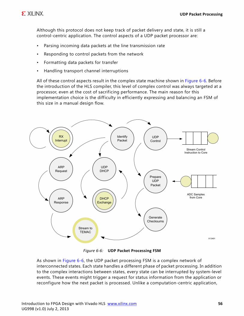
UDP Packet Processing
Although this protocol does not keep track of packet delivery and state, it is still a control-centric application. The control aspects of a UDP packet processor are:
• Parsing incoming data packets at the line transmission rate
• Responding to control packets from the network
• Formatting data packets for transfer
• Handling transport channel interruptions
All of these control aspects result in the complex state machine shown in Figure 6-6. Before the introduction of the HLS compiler, this level of complex control was always targeted at a processor, even at the cost of sacrif icing performance. The main reason for this implementation choice is the diff iculty in efficiently expressing and balancing an FSM of this size in a manual design flow.
As shown in Figure 6-6, the UDP packet processing FSM is a complex network of interconnected states. Each state handles a different phase of packet processing. In addition to the complex interactions between states, every state can be interrupted by system-level events. These events might trigger a request for status information from the application or reconfigure how the next packet is processed. Unlike a computation-centric application,
X-Ref Target - Figure 6-6
Figure 6-6: UDP Packet Processing FSM
Introduction to FPGA Design with Vivado HLS www.xilinx.com 56UG998 (v1.0) July 2, 2013
UDP Packet Processing
there is not a well-defined task size for packet processing. Every packet must be analyzed, which means the duration of a task is infinite as long as there is power to the device. The implementation of the UDP processing FSM begins with the top-level function signature.
Figure 6-7 shows the top-level function signature of a UDP packet processing engine targeted for FPGA implementation using the HLS compiler. In this function, the arrays are used to model physical communication buffers between this module and the rest of the system. Also important to note is the use of the volatile keyword to mark every function variable that is not an array. As shown in Figure 6-6, this controller must be able to handle interrupts from the system during any stage of execution. The problem with this requirement is the function variable behavior as specified in both C and C++.
In C and C++, function variables are sampled and stored in a local copy inside the function memory space when the function call is issued. This means that in addition to potentially storing the same variable in multiple memory spaces, a C/C++ program does not detect a change in the value of a variable until the next function call. The volatile keyword is the language solution to this problem. This construct, which is familiar to the embedded software developer, informs the C/C++ compiler that a variable can change value during the duration of a function call. Therefore, the volatile variable must be accessed directly from the function ports every time it is used in the code. Although this language construct f ixes the data access problem, it does not remove the internal copy of the variable.
The issue of potential duplication of data across memory spaces is resolved by the const qualif ier. When this qualif ier is applied to a function port, the compiler avoids creating the local copy of the variable within the function memory space. Instead, the read or write operation happens directly on the variable port. In the hardware, the usage of a const volatile qualif ier allows the system to react to external inputs during a task and reduces the latency of the reaction.
X-Ref Target - Figure 6-7
Figure 6-7: UDP Processor Function Signature
Introduction to FPGA Design with Vivado HLS www.xilinx.com 57UG998 (v1.0) July 2, 2013
UDP Packet Processing
Figure 6-8 shows the code that encapsulates the main processing of the UDP control FSM.
The execution of the UDP control FSM is divided into an initialization and normal execution phase. The initialization phase occurs as soon as the FPGA implementation comes out of reset. In this phase, status flags are set to default values and the media access control (MAC) address of the block is loaded from memory. The MAC address is the unique network identif ier onto which a dynamic host configuration protocol (DHCP) address is assigned. After the UDP controller can broadcast its address, it starts to process network control packets to request and register an internet protocol (IP) address with the network. After the controller is properly registered in the network, it switches into a normal operating mode and starts generating UDP packets. Aside from the specif ic functionality, this code demonstrates how control and computational coding elements can be combined within a single control-centric application.
The code in Figure 6-8 shows a single level of control hierarchy based on two execution phases. In practice, control-centric applications are more complex than this example and exhibit a hierarchical control structure. The ability to capture a control hierarchy in the same way it is expressed for a processor is one of the key differences between HLS and other software compilers for hardware.
X-Ref Target - Figure 6-8
Figure 6-8: UDP FSM Main Function
Introduction to FPGA Design with Vivado HLS www.xilinx.com 58UG998 (v1.0) July 2, 2013
UDP Packet Processing
Figure 6-9 shows an example of how hierarchical control can be expressed for the HLS compiler. This f igure is a segment of the servlet function in Figure 6-8. The servlet function controls all operation phases of the UDP controller after initialization. As this code shows, the module has constant interaction with system-level signals to determine the next operation. In addition, this coding style maintains the nested case statements and mix of computation functions typical of processor code. This facilitates the capture of functionality in C/C++ and aids in code migration from a processor to an FPGA.
Control-centric applications, such as the UDP processor, can be compiled and implemented on an FPGA with the HLS compiler. Therefore, the decision to implement this type of code is reduced to a resource trade-off between the needs of control code versus the needs of all the other functions in the application. By developing the entire application using the HLS compiler, the user can determine how many resources both the control- and data-centric functions in the design require at different performance points. The capability of the HLS compiler to produce multiple what-if scenarios allows the exploration of design variables, such as throughput versus area versus latency.
X-Ref Target - Figure 6-9
Figure 6-9: Hierarchical Control Regions in UDP Processing
Introduction to FPGA Design with Vivado HLS www.xilinx.com 59UG998 (v1.0) July 2, 2013
Chapter 7
Software Verification and Vivado HLS
OverviewAs with processor compilers, the quality and correctness of the Vivado® HLS compiler output depends on the input software. This chapter reviews the recommended software quality assurance techniques that apply to the Vivado® HLS compiler. It presents examples of typical coding errors and their effect on HLS compilation as well as possible solutions to each problem. It also includes a section on what to do when the behavior of a program cannot be fully verif ied at the C/C++ simulation level.
Software Test BenchVerif ication of any HLS-generated module requires a software test bench. The software test bench serves the following important functions:
• To prove that the software targeted for FPGA implementation runs and does not create a segmentation fault
• To prove the functional correctness of the algorithm
Segmentation faults are an issue in HLS as they are in any other compiler. However, there is a difference in how the coding error that caused the issue is detected. In a processor-based execution, segmentation faults are caused by a program trying to access a memory location that is not known to the processor. The most frequent cause for this error is a user program trying to access a location in memory associated with a pointer address before the memory has been allocated and attached to the pointer. Detection of this error is relatively straightforward at runtime based on the following sequence of events:
1. Processor detects a memory access violation and notif ies the operating system (OS).
2. OS signals the program or process causing the error.
3. After receiving the error signal from the OS, the program terminates and generates a core dump file for analysis.
Introduction to FPGA Design with Vivado HLS www.xilinx.com 60UG998 (v1.0) July 2, 2013
Software Test Bench
In an HLS-generated implementation, it is diff icult to detect a segmentation fault, because there is no processor and no operating system monitoring program execution. The only indicator of a segmentation fault is the appearance of incorrect result values generated by the circuit. This alone is not sufficient to determine the root cause of a segmentation fault, because there are multiple issues that can trigger incorrect result computation.
RECOMMENDED: When working with HLS, it is recommended that the designer ensure that the software test bench compiles and executes the function without issues on a processor. This guarantees that the HLS-generated implementation will not result in a segmentation fault.
The other purpose of the software test bench is to prove the functional correctness of an algorithm targeted towards FPGA execution. For the generated hardware implementation, the HLS compiler guarantees only functional equivalence with the original C/C++ code. Therefore, the existence of a good software test bench is required to minimize efforts in hardware verif ication and validation.
A good software test bench is characterized by the execution of thousands or millions of data set tests on the software implementation of an algorithm. This allows the designer to assert with a high level of confidence that the algorithm was captured properly. However, even with many test vectors, it is sometimes still possible to detect errors in the HLS-generated output during hardware verif ication of an FPGA design. Detecting functional errors during hardware verif ication means that the software test bench was incomplete. Applying the offending test vector to the C/C++ execution reveals the incorrect statement in the algorithm.
IMPORTANT: Errors must not be fixed directly in the generated RTL. Any issues with functional correctness are a direct result of the functional correctness of the software algorithm.
TIP: The software test bench used to exercise an algorithm targeted for FPGA implementation with HLS does not have any coding style restrictions. The software engineer is free to use any valid C/C++ coding style or construct to thoroughly test the functional correctness of an algorithm.
Introduction to FPGA Design with Vivado HLS www.xilinx.com 61UG998 (v1.0) July 2, 2013
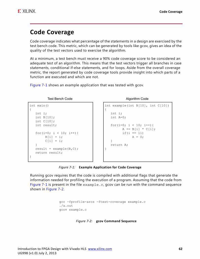
Code Coverage
Code CoverageCode coverage indicates what percentage of the statements in a design are exercised by the test bench code. This metric, which can be generated by tools like gcov, gives an idea of the quality of the test vectors used to exercise the algorithm.
At a minimum, a test bench must receive a 90% code coverage score to be considered an adequate test of an algorithm. This means that the test vectors trigger all branches in case statements, conditional if-else statements, and for loops. Aside from the overall coverage metric, the report generated by code coverage tools provide insight into which parts of a function are executed and which are not.
Figure 7-1 shows an example application that was tested with gcov.
Running gcov requires that the code is compiled with additional flags that generate the information needed for profiling the execution of a program. Assuming that the code from Figure 7-1 is present in the f ile example.c, gcov can be run with the command sequence shown in Figure 7-2.
X-Ref Target - Figure 7-1
Figure 7-1: Example Application for Code Coverage
X-Ref Target - Figure 7-2
Figure 7-2: gcov Command Sequence
Introduction to FPGA Design with Vivado HLS www.xilinx.com 62UG998 (v1.0) July 2, 2013
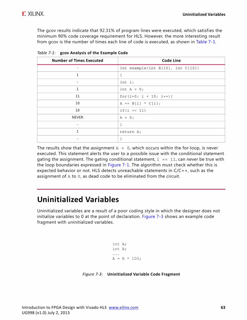
Uninitialized Variables
The gcov results indicate that 92.31% of program lines were executed, which satisf ies the minimum 90% code coverage requirement for HLS. However, the more interesting result from gcov is the number of times each line of code is executed, as shown in Table 7-1.
The results show that the assignment A = 0, which occurs within the for-loop, is never executed. This statement alerts the user to a possible issue with the conditional statement gating the assignment. The gating conditional statement, i == 11, can never be true with the loop boundaries expressed in Figure 7-1. The algorithm must check whether this is expected behavior or not. HLS detects unreachable statements in C/C++, such as the assignment of A to 0, as dead code to be eliminated from the circuit.
Uninitialized VariablesUninitialized variables are a result of a poor coding style in which the designer does not initialize variables to 0 at the point of declaration. Figure 7-3 shows an example code fragment with uninitialized variables.
Table 7-1: gcov Analysis of the Example Code
Number of Times Executed Code Line
- int example(int B[10], int C[10])
1 {
- int i;
1 int A = 0;
11 for(i=0; i < 10; i++){
10 A += B[i] * C[i];
10 if(i == 11)
NEVER A = 0;
- }
1 return A;
- }
X-Ref Target - Figure 7-3
Figure 7-3: Uninitialized Variable Code Fragment
Introduction to FPGA Design with Vivado HLS www.xilinx.com 63UG998 (v1.0) July 2, 2013
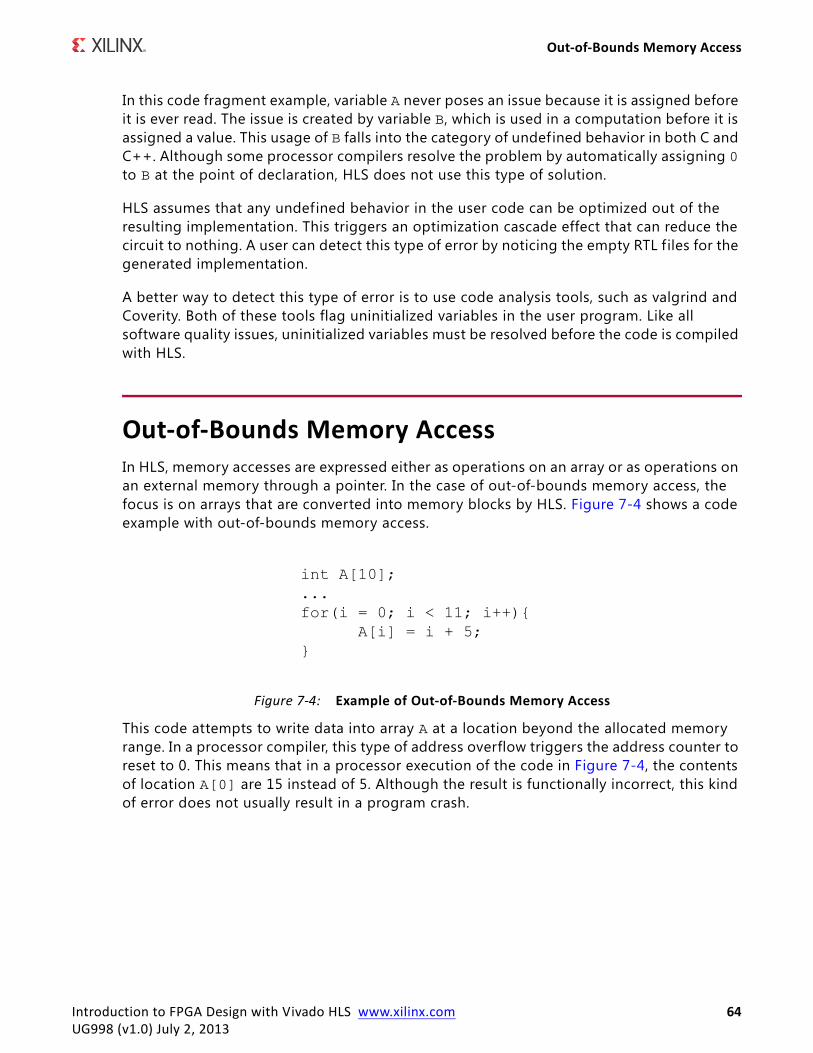
Out-of-Bounds Memory Access
In this code fragment example, variable A never poses an issue because it is assigned before it is ever read. The issue is created by variable B, which is used in a computation before it is assigned a value. This usage of B falls into the category of undefined behavior in both C and C++. Although some processor compilers resolve the problem by automatically assigning 0 to B at the point of declaration, HLS does not use this type of solution.
HLS assumes that any undefined behavior in the user code can be optimized out of the resulting implementation. This triggers an optimization cascade effect that can reduce the circuit to nothing. A user can detect this type of error by noticing the empty RTL files for the generated implementation.
A better way to detect this type of error is to use code analysis tools, such as valgrind and Coverity. Both of these tools flag uninitialized variables in the user program. Like all software quality issues, uninitialized variables must be resolved before the code is compiled with HLS.
Out-of-Bounds Memory AccessIn HLS, memory accesses are expressed either as operations on an array or as operations on an external memory through a pointer. In the case of out-of-bounds memory access, the focus is on arrays that are converted into memory blocks by HLS. Figure 7-4 shows a code example with out-of-bounds memory access.
This code attempts to write data into array A at a location beyond the allocated memory range. In a processor compiler, this type of address overflow triggers the address counter to reset to 0. This means that in a processor execution of the code in Figure 7-4, the contents of location A[0] are 15 instead of 5. Although the result is functionally incorrect, this kind of error does not usually result in a program crash.
X-Ref Target - Figure 7-4
Figure 7-4: Example of Out-of-Bounds Memory Access
Introduction to FPGA Design with Vivado HLS www.xilinx.com 64UG998 (v1.0) July 2, 2013
Co-Simulation
With HLS, accessing an invalid address triggers a series of events that result in an irrecoverable runtime error in the generated circuit. Because the HLS implementation assumes that the software algorithm was properly verif ied, error recovery logic is not included in the generated FPGA implementation. Therefore, an invalid memory address is generated by the implementation of the code in Figure 7-4 to the BRAM resource element storing the value of array A. The BRAM then issues an error condition that is not expected by the HLS implementation, and the error is left unattended. The unattended error from the BRAM causes the system to hang and can only be resolved with a device reboot.
To catch cases like this before circuit compilation, it is recommended that the tool is executed through a dynamic code checker such as valgrind. Valgrind is a suite of tools designed to check and profile the quality of a C/C++ program. The valgrind Memcheck tool executes a compiled C/C++ program and monitors all memory operations during execution. This tool flags the following critical issues:
• Use of uninitialized variables (Figure 7-3)
• Invalid memory access requests (Figure 7-4)
RECOMMENDED: Before using HLS to compile a software function for FPGA execution, it is recommended that all of the issues flagged by a dynamic code checker are resolved by the designer.
Co-SimulationTools for C/C++ program analysis and functionality testing catch most of the issues that affect an HLS implementation. However, these tools are unable to verify whether a sequential C/C++ program maintains functional correctness after parallelization. This issue is resolved in the HLS compiler by the process of co-simulation.
Co-simulation is a process in which the generated FPGA implementation is exercised by the same C/C++ test bench used during software simulation. HLS handles the communication between the C/C++ test bench and the generated RTL in a manner that is transparent to the user. As part of this process, HLS invokes a hardware simulator, such as the Vivado simulator, to emulate how the RTL will function on the device. The main purpose of this simulation is to check that the parallelization guidance provided by the user did not break the functional correctness of the algorithm.
Introduction to FPGA Design with Vivado HLS www.xilinx.com 65UG998 (v1.0) July 2, 2013
Co-Simulation
By default, HLS obeys all algorithm dependencies before parallelization to ensure functional equivalence with the original C/C++ representation. In cases where an algorithm dependence cannot be fully analyzed, HLS takes a conservative approach and obeys dependence. This can lead the compiler to generate a conservative implementation that does not achieve the target performance goals of the application. Figure 7-5 shows an example of the code that triggers the conservative behavior in HLS.
The code shows a loop operating on arrays A and B, and the analysis issue occurs on array A. The index into array A depends on loop variable i and variable k . In this example, variable k represents a function parameter of unknown value at compile time. Therefore, HLS cannot prove that the write into A[k+i] occurs at a different location than the read of A[i] used in computing B[i]. Based on this uncertainty, HLS assumes an algorithmic dependence that forces the computation of A[k+i] and B[i] to occur in sequential order as expressed in the original C/C++ source. The user has the ability to override this dependence and force HLS to generate a circuit in which A[k+i] and B[i] are computed in parallel. The effects of this override only affect the generated circuit and can therefore only be verif ied by co-simulation.
When using co-simulation, it is important to remember that this is a simulation of parallel hardware being executed on a processor. Therefore, it is approximately 10,000 times slower than C/C++ simulation. It is also important to remember that the purpose of co-simulation is not to verify the functional correctness of an algorithm. Instead, the purpose is to check that the algorithm was not broken by user guidance to the HLS compiler.
RECOMMENDED: It is recommended that co-simulation only be run on a subset of the test vectors used during algorithm functional verification.
X-Ref Target - Figure 7-5
Figure 7-5: Dependence Example that Triggers Conservative HLS Implementation
Introduction to FPGA Design with Vivado HLS www.xilinx.com 66UG998 (v1.0) July 2, 2013
When C/C++ Verification Is Not Possible
When C/C++ Verification Is Not PossibleThe majority of use cases for HLS are in algorithms that can be fully verif ied for functional correctness with a C/C++ simulation. However, there are still some cases where the C/C++ representation of an algorithm cannot be fully verif ied before HLS compilation. Figure 7-6 shows an example of this type of code.
This code shows a snippet of a UDP packet processing engine described in C. In this example, all the pointers are declared with the volatile keyword. The usage of the volatile keyword, which is common in device driver development, alerts the compiler that the pointers are connected to storage elements that might change during the execution of the function. This kind of pointer must be read or written every time it is specified in the source code. Traditional compiler optimizations to coalesce pointer accesses are also turned off by the volatile keyword.
The issue with volatile data is that the behavior of the code cannot be fully verif ied in a C/C++ simulation. C/C++ simulation does not have the ability to change the value of a pointer in the middle of the execution of the function under test. Therefore, this type of code can only be fully verif ied in an RTL simulation after HLS compilation. The user must write an RTL test bench to test the generated circuit in all possible cases for each volatile pointer in the C/C++ source. The use of co-simulation is not applicable in this case, because it is limited by the test vectors that can be used in a C/C++ simulation.
X-Ref Target - Figure 7-6
Figure 7-6: Code Example Using Volatile Types
Introduction to FPGA Design with Vivado HLS www.xilinx.com 67UG998 (v1.0) July 2, 2013
Chapter 8
Integration of Multiple Programs
OverviewJust as most processors run multiple programs to execute an application, an FPGA instantiates multiple programs or modules to execute an application. This chapter focuses on how to connect multiple modules in an FPGA and how to control these modules using a processor. The example in this chapter uses the Xilinx® Zynq®-7000 AP SoC to demonstrate interconnection between a processor and FPGA fabric.
The Zynq-7000 AP SoC is the f irst in a new class of devices targeted at low power software execution. This device combines an ARM® Cortex™-A9 multi-core processor with FPGA fabric in a single chip. The level of integration in this device eliminates the communication latencies and bottlenecks associated with co-processor or acceleration solutions. This device also eliminates the need for a PCIe® bridge to transfer data between the code running on the processor and the code compiled by Vivado® HLS for the FPGA. Instead, the interconnection of these two computation domains is through the use of the Advanced eXtensible Interface (AXI) protocol.
AXIAXI is part of the ARM Advanced Microcontroller Bus Architecture (AMBA®) family of microcontroller buses. This standard defines how modules in a system transfer data between one another. The AXI communication use cases that apply to an application running on the Zynq-7000 AP SoC are:
• Memory mapped slave
• Memory mapped master
• Direct point-to-point stream
Note: For more information on AXI and how it is implemented for Xilinx FPGAs, see the AXI Reference Guide (UG761) [Ref 2].
Introduction to FPGA Design with Vivado HLS www.xilinx.com 68UG998 (v1.0) July 2, 2013
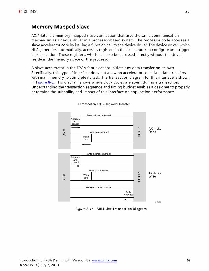
AXI
Memory Mapped SlaveAXI4-Lite is a memory mapped slave connection that uses the same communication mechanism as a device driver in a processor-based system. The processor code accesses a slave accelerator core by issuing a function call to the device driver. The device driver, which HLS generates automatically, accesses registers in the accelerator to configure and trigger task execution. These registers, which can also be accessed directly without the driver, reside in the memory space of the processor.
A slave accelerator in the FPGA fabric cannot initiate any data transfer on its own. Specif ically, this type of interface does not allow an accelerator to initiate data transfers with main memory to complete its task. The transaction diagram for this interface is shown in Figure 8-1. This diagram shows where clock cycles are spent during a transaction. Understanding the transaction sequence and timing budget enables a designer to properly determine the suitability and impact of this interface on application performance.
X-Ref Target - Figure 8-1
Figure 8-1: AXI4-Lite Transaction Diagram
Introduction to FPGA Design with Vivado HLS www.xilinx.com 69UG998 (v1.0) July 2, 2013
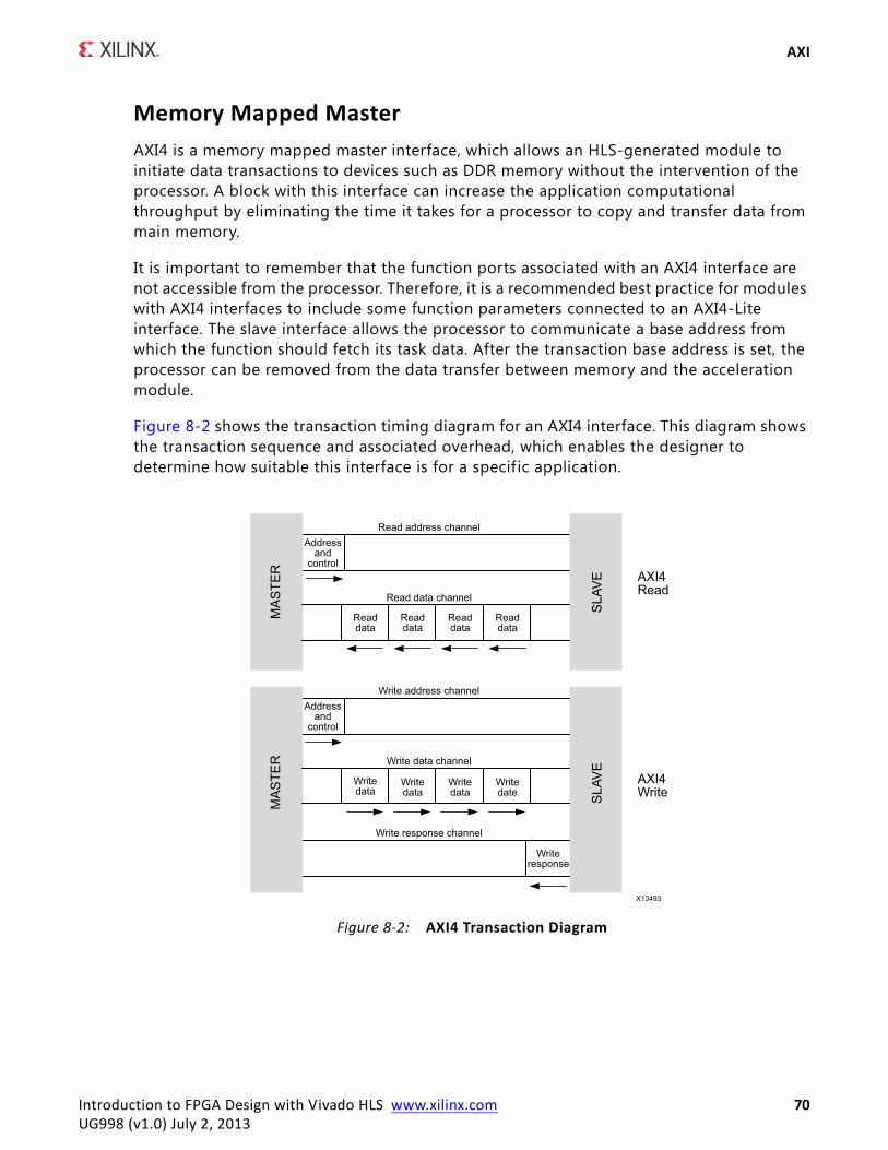
AXI
Memory Mapped MasterAXI4 is a memory mapped master interface, which allows an HLS-generated module to initiate data transactions to devices such as DDR memory without the intervention of the processor. A block with this interface can increase the application computational throughput by eliminating the time it takes for a processor to copy and transfer data from main memory.
It is important to remember that the function ports associated with an AXI4 interface are not accessible from the processor. Therefore, it is a recommended best practice for modules with AXI4 interfaces to include some function parameters connected to an AXI4-Lite interface. The slave interface allows the processor to communicate a base address from which the function should fetch its task data. After the transaction base address is set, the processor can be removed from the data transfer between memory and the acceleration module.
Figure 8-2 shows the transaction timing diagram for an AXI4 interface. This diagram shows the transaction sequence and associated overhead, which enables the designer to determine how suitable this interface is for a specific application.
X-Ref Target - Figure 8-2
Figure 8-2: AXI4 Transaction Diagram
Introduction to FPGA Design with Vivado HLS www.xilinx.com 70UG998 (v1.0) July 2, 2013
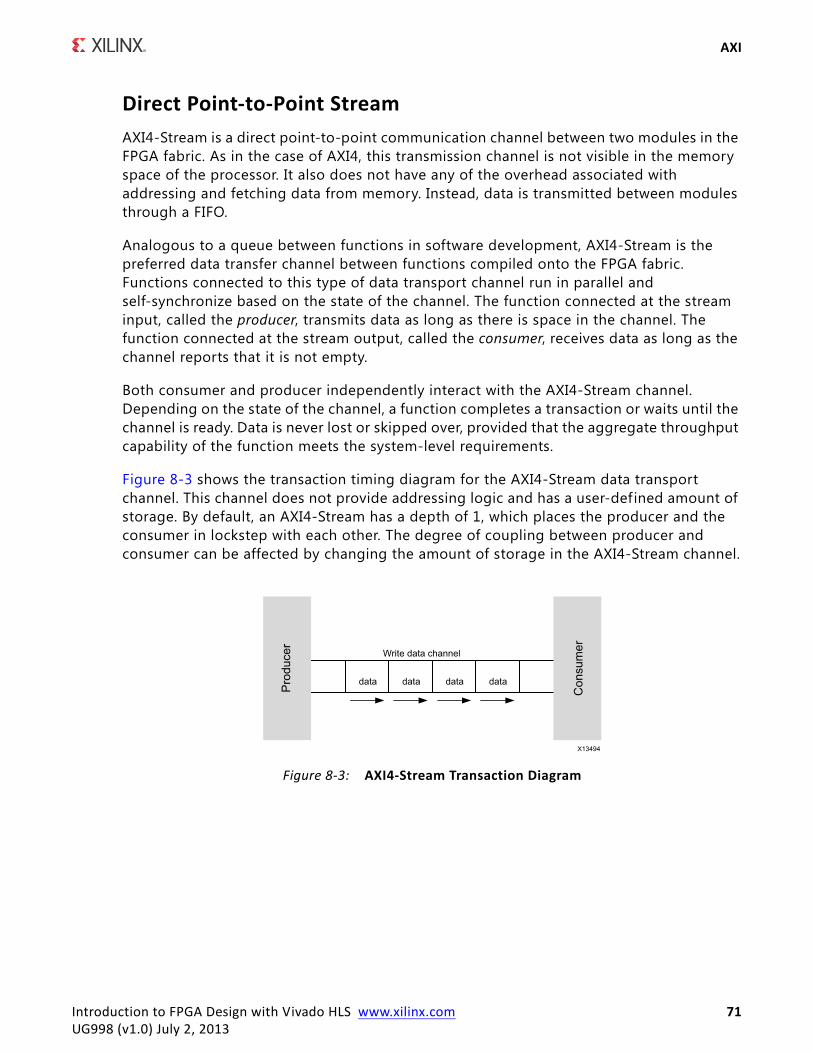
AXI
Direct Point-to-Point StreamAXI4-Stream is a direct point-to-point communication channel between two modules in the FPGA fabric. As in the case of AXI4, this transmission channel is not visible in the memory space of the processor. It also does not have any of the overhead associated with addressing and fetching data from memory. Instead, data is transmitted between modules through a FIFO.
Analogous to a queue between functions in software development, AXI4-Stream is the preferred data transfer channel between functions compiled onto the FPGA fabric. Functions connected to this type of data transport channel run in parallel and self-synchronize based on the state of the channel. The function connected at the stream input, called the producer, transmits data as long as there is space in the channel. The function connected at the stream output, called the consumer, receives data as long as the channel reports that it is not empty.
Both consumer and producer independently interact with the AXI4-Stream channel. Depending on the state of the channel, a function completes a transaction or waits until the channel is ready. Data is never lost or skipped over, provided that the aggregate throughput capability of the function meets the system-level requirements.
Figure 8-3 shows the transaction timing diagram for the AXI4-Stream data transport channel. This channel does not provide addressing logic and has a user-defined amount of storage. By default, an AXI4-Stream has a depth of 1, which places the producer and the consumer in lockstep with each other. The degree of coupling between producer and consumer can be affected by changing the amount of storage in the AXI4-Stream channel.
X-Ref Target - Figure 8-3
Figure 8-3: AXI4-Stream Transaction Diagram
Introduction to FPGA Design with Vivado HLS www.xilinx.com 71UG998 (v1.0) July 2, 2013
Design Example: Application Running on a Zynq-7000 AP SoC
Design Example: Application Running on a Zynq-7000 AP SoCThis design example shows how to take processor code and transform it into an application that runs on a Zynq-7000 AP SoC. This example walks through the following steps in the migration process:
• Analyzing and partitioning the processor code
• Compiling the program in Vivado HLS
• Composing the system in Vivado IP integrator
• Connecting processor code and FPGA fabric functions
Note: The ARM Cortex-A9 processor inside the Zynq-7000 device can support both single program execution and complete operating systems, such as Linux. In either operating case, the steps required to build the application are the same. Therefore, this example focuses on the single program execution model, which demonstrates the application migration process.
Analyzing and Partitioning the Processor Code
Most software applications targeted for a Zynq-7000 device begin as applications executing on either a standard x86 processor or a DSP processor. Therefore, the f irst step in migrating a design is to compile the program for the ARM Cortex-A9 processor and analyze its performance. The performance analysis data of a program running on the ARM processor guides the designer in choosing how to partition the original code between processor and FPGA fabric.
Introduction to FPGA Design with Vivado HLS www.xilinx.com 72UG998 (v1.0) July 2, 2013
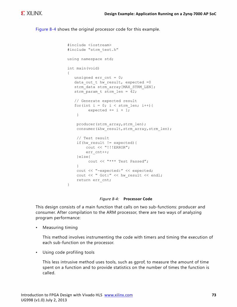
Design Example: Application Running on a Zynq-7000 AP SoC
Figure 8-4 shows the original processor code for this example.
This design consists of a main function that calls on two sub-functions: producer and consumer. After compilation to the ARM processor, there are two ways of analyzing program performance:
• Measuring timing
This method involves instrumenting the code with timers and timing the execution of each sub-function on the processor.
• Using code profiling tools
This less intrusive method uses tools, such as gprof, to measure the amount of time spent on a function and to provide statistics on the number of times the function is called.
X-Ref Target - Figure 8-4
Figure 8-4: Processor Code
Introduction to FPGA Design with Vivado HLS www.xilinx.com 73UG998 (v1.0) July 2, 2013
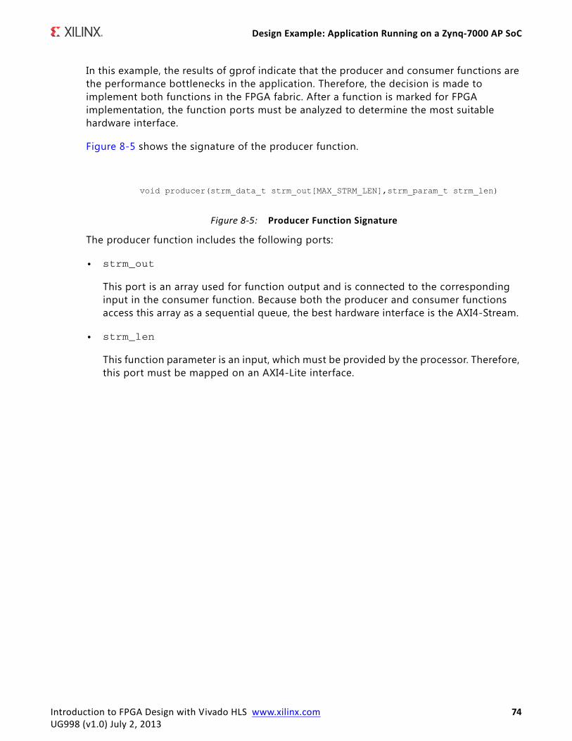
Design Example: Application Running on a Zynq-7000 AP SoC
In this example, the results of gprof indicate that the producer and consumer functions are the performance bottlenecks in the application. Therefore, the decision is made to implement both functions in the FPGA fabric. After a function is marked for FPGA implementation, the function ports must be analyzed to determine the most suitable hardware interface.
Figure 8-5 shows the signature of the producer function.
The producer function includes the following ports:
• strm_out
This port is an array used for function output and is connected to the corresponding input in the consumer function. Because both the producer and consumer functions access this array as a sequential queue, the best hardware interface is the AXI4-Stream.
• strm_len
This function parameter is an input, which must be provided by the processor. Therefore, this port must be mapped on an AXI4-Lite interface.
X-Ref Target - Figure 8-5
Figure 8-5: Producer Function Signature
Introduction to FPGA Design with Vivado HLS www.xilinx.com 74UG998 (v1.0) July 2, 2013
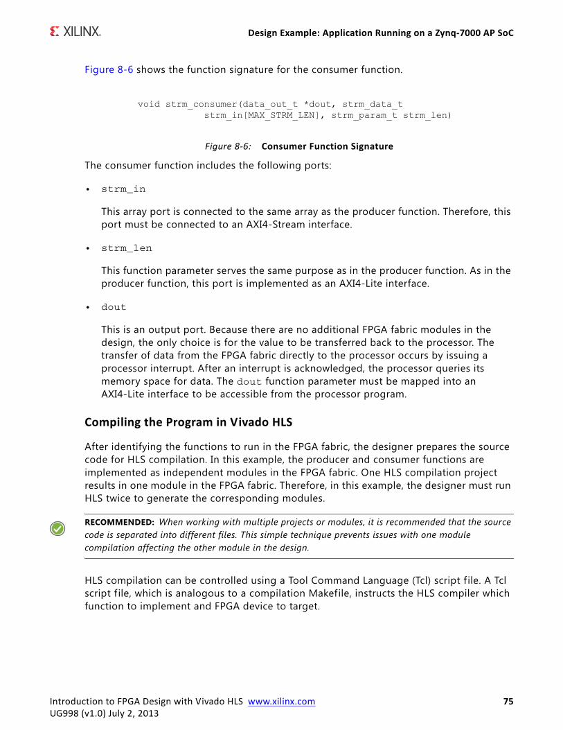
Design Example: Application Running on a Zynq-7000 AP SoC
Figure 8-6 shows the function signature for the consumer function.
The consumer function includes the following ports:
• strm_in
This array port is connected to the same array as the producer function. Therefore, this port must be connected to an AXI4-Stream interface.
• strm_len
This function parameter serves the same purpose as in the producer function. As in the producer function, this port is implemented as an AXI4-Lite interface.
• dout
This is an output port. Because there are no additional FPGA fabric modules in the design, the only choice is for the value to be transferred back to the processor. The transfer of data from the FPGA fabric directly to the processor occurs by issuing a processor interrupt. After an interrupt is acknowledged, the processor queries its memory space for data. The dout function parameter must be mapped into an AXI4-Lite interface to be accessible from the processor program.
Compiling the Program in Vivado HLS
After identifying the functions to run in the FPGA fabric, the designer prepares the source code for HLS compilation. In this example, the producer and consumer functions are implemented as independent modules in the FPGA fabric. One HLS compilation project results in one module in the FPGA fabric. Therefore, in this example, the designer must run HLS twice to generate the corresponding modules.
RECOMMENDED: When working with multiple projects or modules, it is recommended that the source code is separated into different files. This simple technique prevents issues with one module compilation affecting the other module in the design.
HLS compilation can be controlled using a Tool Command Language (Tcl) script f ile. A Tcl script f ile, which is analogous to a compilation Makefile, instructs the HLS compiler which function to implement and FPGA device to target.
X-Ref Target - Figure 8-6
Figure 8-6: Consumer Function Signature
Introduction to FPGA Design with Vivado HLS www.xilinx.com 75UG998 (v1.0) July 2, 2013
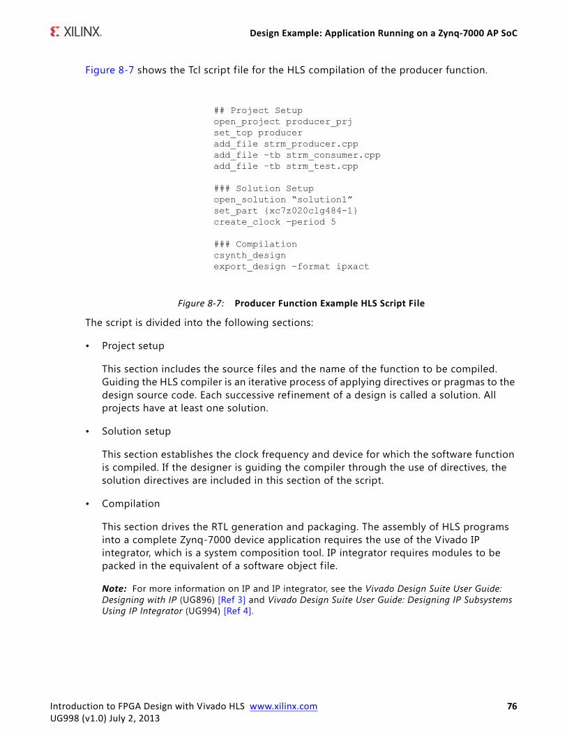
Design Example: Application Running on a Zynq-7000 AP SoC
Figure 8-7 shows the Tcl script f ile for the HLS compilation of the producer function.
The script is divided into the following sections:
• Project setup
This section includes the source f iles and the name of the function to be compiled. Guiding the HLS compiler is an iterative process of applying directives or pragmas to the design source code. Each successive refinement of a design is called a solution. All projects have at least one solution.
• Solution setup
This section establishes the clock frequency and device for which the software function is compiled. If the designer is guiding the compiler through the use of directives, the solution directives are included in this section of the script.
• Compilation
This section drives the RTL generation and packaging. The assembly of HLS programs into a complete Zynq-7000 device application requires the use of the Vivado IP integrator, which is a system composition tool. IP integrator requires modules to be packed in the equivalent of a software object f ile.
Note: For more information on IP and IP integrator, see the Vivado Design Suite User Guide: Designing with IP (UG896) [Ref 3] and Vivado Design Suite User Guide: Designing IP Subsystems Using IP Integrator (UG994) [Ref 4].
X-Ref Target - Figure 8-7
Figure 8-7: Producer Function Example HLS Script File
Introduction to FPGA Design with Vivado HLS www.xilinx.com 76UG998 (v1.0) July 2, 2013
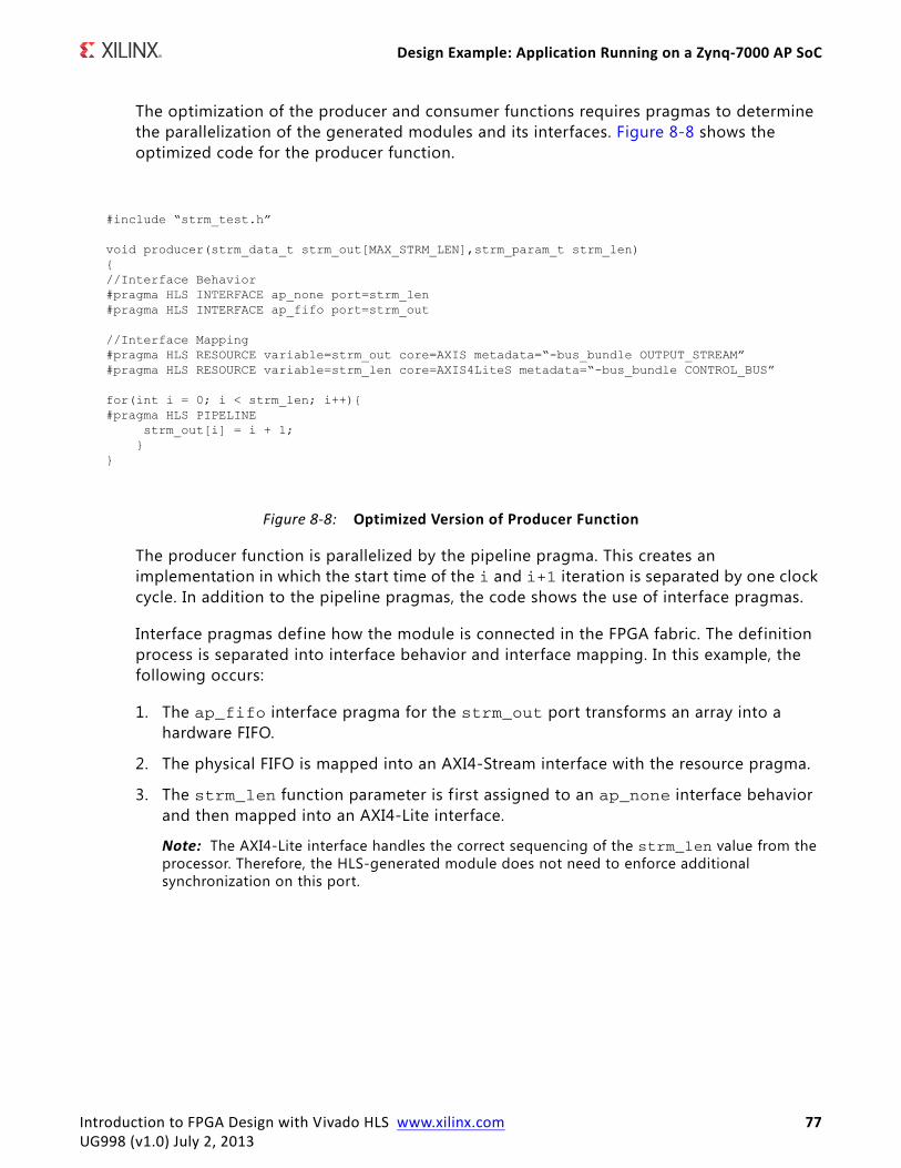
Design Example: Application Running on a Zynq-7000 AP SoC
The optimization of the producer and consumer functions requires pragmas to determine the parallelization of the generated modules and its interfaces. Figure 8-8 shows the optimized code for the producer function.
The producer function is parallelized by the pipeline pragma. This creates an implementation in which the start time of the i and i+1 iteration is separated by one clock cycle. In addition to the pipeline pragmas, the code shows the use of interface pragmas.
Interface pragmas define how the module is connected in the FPGA fabric. The definition process is separated into interface behavior and interface mapping. In this example, the following occurs:
1. The ap_fifo interface pragma for the strm_out port transforms an array into a hardware FIFO.
2. The physical FIFO is mapped into an AXI4-Stream interface with the resource pragma.
3. The strm_len function parameter is f irst assigned to an ap_none interface behavior and then mapped into an AXI4-Lite interface.
Note: The AXI4-Lite interface handles the correct sequencing of the strm_len value from the processor. Therefore, the HLS-generated module does not need to enforce additional synchronization on this port.
X-Ref Target - Figure 8-8
Figure 8-8: Optimized Version of Producer Function
Introduction to FPGA Design with Vivado HLS www.xilinx.com 77UG998 (v1.0) July 2, 2013
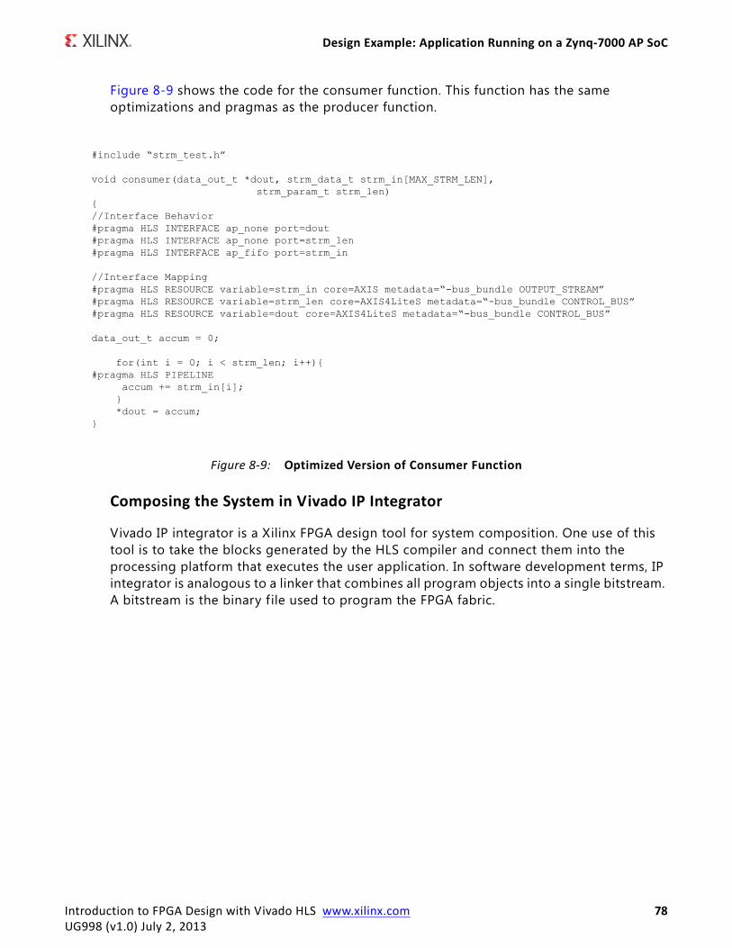
Design Example: Application Running on a Zynq-7000 AP SoC
Figure 8-9 shows the code for the consumer function. This function has the same optimizations and pragmas as the producer function.
Composing the System in Vivado IP Integrator
Vivado IP integrator is a Xilinx FPGA design tool for system composition. One use of this tool is to take the blocks generated by the HLS compiler and connect them into the processing platform that executes the user application. In software development terms, IP integrator is analogous to a linker that combines all program objects into a single bitstream. A bitstream is the binary file used to program the FPGA fabric.
X-Ref Target - Figure 8-9
Figure 8-9: Optimized Version of Consumer Function
Introduction to FPGA Design with Vivado HLS www.xilinx.com 78UG998 (v1.0) July 2, 2013
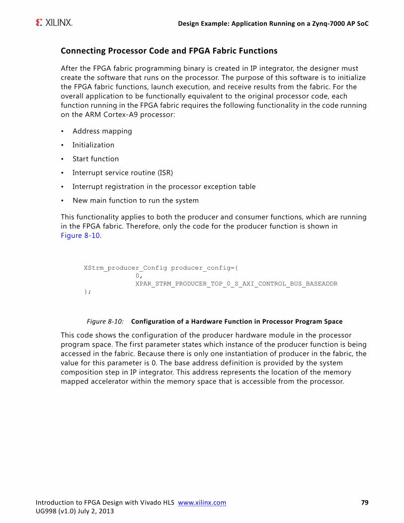
Design Example: Application Running on a Zynq-7000 AP SoC
Connecting Processor Code and FPGA Fabric Functions
After the FPGA fabric programming binary is created in IP integrator, the designer must create the software that runs on the processor. The purpose of this software is to initialize the FPGA fabric functions, launch execution, and receive results from the fabric. For the overall application to be functionally equivalent to the original processor code, each function running in the FPGA fabric requires the following functionality in the code running on the ARM Cortex-A9 processor:
• Address mapping
• Initialization
• Start function
• Interrupt service routine (ISR)
• Interrupt registration in the processor exception table
• New main function to run the system
This functionality applies to both the producer and consumer functions, which are running in the FPGA fabric. Therefore, only the code for the producer function is shown in Figure 8-10.
This code shows the configuration of the producer hardware module in the processor program space. The f irst parameter states which instance of the producer function is being accessed in the fabric. Because there is only one instantiation of producer in the fabric, the value for this parameter is 0. The base address definition is provided by the system composition step in IP integrator. This address represents the location of the memory mapped accelerator within the memory space that is accessible from the processor.
X-Ref Target - Figure 8-10
Figure 8-10: Configuration of a Hardware Function in Processor Program Space
Introduction to FPGA Design with Vivado HLS www.xilinx.com 79UG998 (v1.0) July 2, 2013
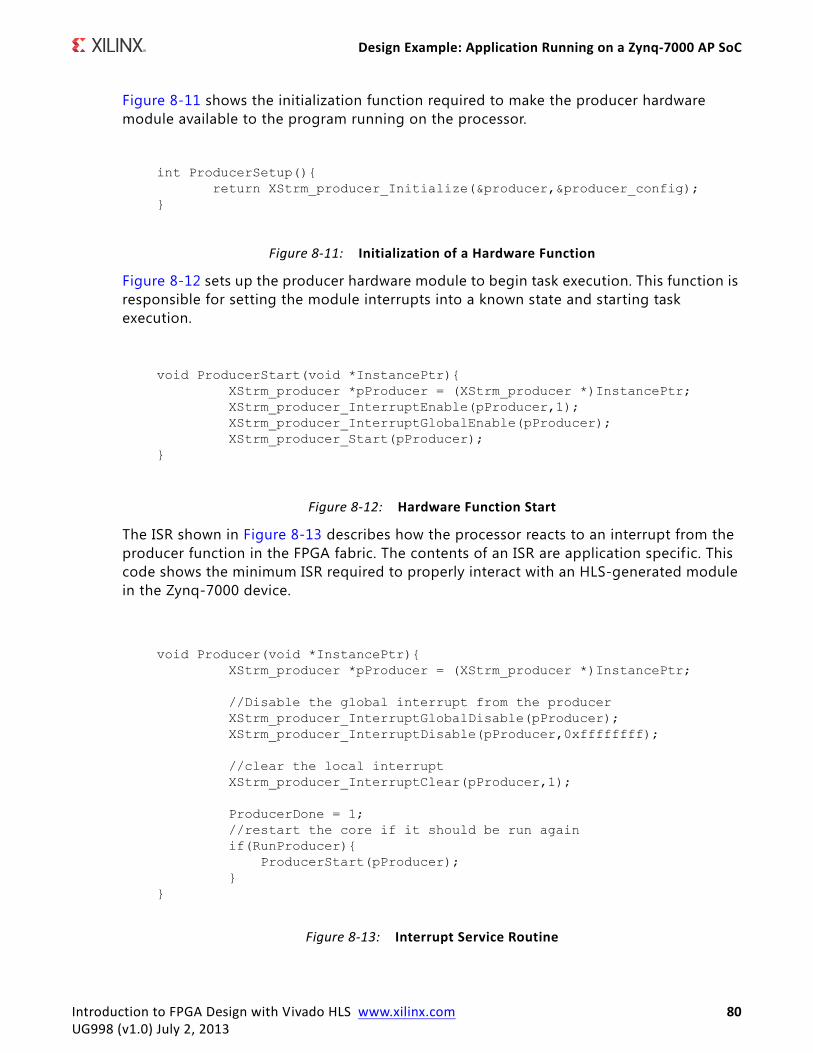
Design Example: Application Running on a Zynq-7000 AP SoC
Figure 8-11 shows the initialization function required to make the producer hardware module available to the program running on the processor.
Figure 8-12 sets up the producer hardware module to begin task execution. This function is responsible for setting the module interrupts into a known state and starting task execution.
The ISR shown in Figure 8-13 describes how the processor reacts to an interrupt from the producer function in the FPGA fabric. The contents of an ISR are application specific. This code shows the minimum ISR required to properly interact with an HLS-generated module in the Zynq-7000 device.
X-Ref Target - Figure 8-11
Figure 8-11: Initialization of a Hardware Function
X-Ref Target - Figure 8-12
Figure 8-12: Hardware Function Start
X-Ref Target - Figure 8-13
Figure 8-13: Interrupt Service Routine
Introduction to FPGA Design with Vivado HLS www.xilinx.com 80UG998 (v1.0) July 2, 2013
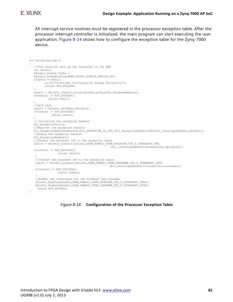
Design Example: Application Running on a Zynq-7000 AP SoC
All interrupt service routines must be registered in the processor exception table. After the processor interrupt controller is initialized, the main program can start executing the user application. Figure 8-14 shows how to configure the exception table for the Zynq-7000 device.
X-Ref Target - Figure 8-14
Figure 8-14: Configuration of the Processor Exception Table
Introduction to FPGA Design with Vivado HLS www.xilinx.com 81UG998 (v1.0) July 2, 2013
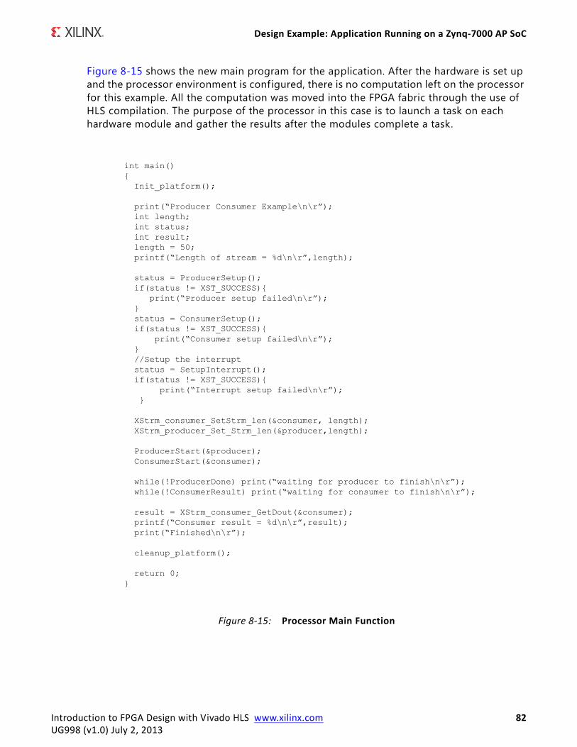
Design Example: Application Running on a Zynq-7000 AP SoC
Figure 8-15 shows the new main program for the application. After the hardware is set up and the processor environment is configured, there is no computation left on the processor for this example. All the computation was moved into the FPGA fabric through the use of HLS compilation. The purpose of the processor in this case is to launch a task on each hardware module and gather the results after the modules complete a task.
X-Ref Target - Figure 8-15
Figure 8-15: Processor Main Function
Introduction to FPGA Design with Vivado HLS www.xilinx.com 82UG998 (v1.0) July 2, 2013
Chapter 9
Verification of a Complete Application
OverviewIn FPGA design, a complete application refers to a hardware system that implements the functionality captured by the software representation of a design. There are two main categories of systems that can be built on an FPGA using the Vivado® HLS compiler:
• Standalone compute systems
• Processor-based systems
Standalone Compute SystemsThe standalone compute system is an FPGA implementation created by one or more HLS-generated modules connected together to implement a software application. In these types of systems, the configuration of the algorithm is f ixed and loaded during device configuration. The modules generated by the HLS compiler are connected to external FPGA pins for data transmit and receive transactions. This is the easiest kind of system to verify. The verif ication of a standalone system is divided into the following stages:
• Module verif ication
• Connectivity verif ication
• Application verif ication
• Device validation
Module VerificationModule verif ication of an HLS-generated block is covered in detail in Chapter 7, Software Verif ication and Vivado HLS. After the block is fully verif ied for functional correctness in both software and co-simulation, the designer must test the block for in system error tolerance.
Introduction to FPGA Design with Vivado HLS www.xilinx.com 83UG998 (v1.0) July 2, 2013
Standalone Compute Systems
Both software simulation and co-simulation are focused on testing the functional correctness of an algorithm in isolation. That is, the algorithm and compiled module are tested to ensure correct functionality when all inputs and outputs are handled in an ideal manner. This thorough level of testing helps to ensure correctness after data is supplied to the module. It also helps to reduce the verif ication burden of later stages by eliminating the internal processing core of a module as a possible source of error. The only module-level issue that is not handled by this methodology is verif ication that the module can recover fully from incorrect handshaking at its interfaces.
In-system testing tests how the HLS-generated module reacts to incorrect toggling of its input and output ports. The purpose of this testing is to eliminate I/O behavior as an error source that can crash or otherwise adversely affect the module under test. The types of improper use cases tested in this methodology are:
• Erratic clock signal toggling
• Reset operation and random reset pulsing
• Input ports receiving data at different rates
• Output ports being sampled at different rates
• Interface protocol violations
These tests, which are examples of system-level behavior, ensure that the HLS-generated module functions as expected under all circumstances. The amount of testing required at this stage depends on the types of interfaces and the integration methodology. By using HLS default settings to generate AXI-compliant interfaces, the designer can avoid writing an exhaustive test bench of incorrect system-level behavior. AXI-compliant interfaces are fully tested and verif ied by the developers of the HLS compiler.
Connectivity VerificationConnectivity verif ication is a sequence of tests to check that the modules in an application are properly connected to each other. As with module verif ication, the amount of testing required depends on the system integration methodology. As discussed in Chapter 8, Integration of Multiple Programs, applications can be assembled either manually or with the assistance of FPGA design tools.
FPGA design tool assistance is provided in both the Xilinx® System Generator and Vivado IP integrator design flows. These graphical module connection tools handle all the aspects related to module connection. As part of these flows, each tool checks the port types and protocol compliance of each module in the application. If each module has undergone module verif ication, there is no need for additional user-directed connectivity testing with either of these flows.
Introduction to FPGA Design with Vivado HLS www.xilinx.com 84UG998 (v1.0) July 2, 2013
Standalone Compute Systems
The manual integration flow requires the user to write an application top-level module in RTL and manually connect the RTL ports of every module that makes up an application. This is the most error-prone flow and must be verif ied. The amount of testing required can be decreased by using HLS compiler defaults and generating AXI interfaces for every module port.
For systems built around AXI interfaces, the connectivity can be verif ied through the use of a bus functional model (BFM). The BFM provides the Xilinx-verif ied behavior of AXI buses and point-to-point connections. These models can be used for traff ic generators, which help prove the correct connection of HLS-generated modules as part of an RTL simulation.
IMPORTANT: It is important to remember that the purpose of this simulation is only to check connectivity and the proper flow of data through the system. The connectivity verification step does not verify the functional correctness of the application.
Application VerificationApplication verif ication is the f inal step before running the application on the FPGA device. The previous steps in the flow focused on checking the quality of the individual algorithms that compose an application as well as checking that everything is connected properly. Application verif ication focuses on checking that the original software model matches the results of the FPGA implementation. If the application is composed of a single HLS-generated module, this stage is the same as module verif ication. In cases where the application is composed of two or more HLS-generated modules, the verif ication process starts with the original software model.
The designer must extract application input and output test vectors from the software model to be used in an RTL simulation. Because the construction of the hardware implementation is verif ied in multiple stages, the application verif ication does not need to be an exhaustive simulation. The simulation can run as many test vectors as needed for the designer to feel confident in the FPGA implementation.
Device ValidationAfter an application is assembled in RTL using either automated or manual integration flows, the design goes through an additional compilation stage to generate the binary or bitstream required to program the FPGA. In the terminology of FPGA design, the compilation of RTL into a bitstream is referred to as logic synthesis, implementation, and bitstream generation. After the bitstream is generated, the FPGA device can be programmed. The application is validated after the hardware runs correctly for an amount of time specif ied by the designer.
Introduction to FPGA Design with Vivado HLS www.xilinx.com 85UG998 (v1.0) July 2, 2013
Processor-Based Systems
Processor-Based SystemsFor the module and connectivity verif ication stages, the verif ication flow for a processor-based system is the same as the standalone system. The major difference is that a portion of the application is running on the processor. In the Zynq®-7000 AP SoC, this means that part of the application runs on the embedded ARM® Cortex™-A9 processors and part is compiled by HLS to execute on the FPGA fabric. This partitioning presents a verif ication challenge that can be addressed through the use of the following technologies:
• Hardware in the loop (HIL) verif ication
• Virtual platform (VP) verif ication
Hardware in the Loop VerificationHIL verif ication is a verif ication methodology in which the simulation of part of the system under test is executed in the FPGA fabric. In the Zynq-7000 AP SoC, the application code targeted for the processor is executed on the actual ARM Cortex-A9 processor in the device. The code compiled with HLS is executed in an RTL simulation.
Figure 9-1 shows an overview of HIL verif ication for the Zynq-7000 device. The system in this f igure is an experimental setup that includes the ZC702 evaluation board, which is a currently available commercial board, and the Vivado simulator. This f igure also introduces the concept of a processing system (PS) and a programmable logic (PL) unit. The PS refers to the dual ARM Cortex-A9 processor, which is also called the processing subsystem. The PL refers to the FPGA logic inside the Zynq-7000 device, which is the portion of the device onto which the HLS-generated modules are mapped.
TIP: HIL verification requires a board to gain access to the processor, and this technology works on any Zynq-7000 AP SoC board.
Introduction to FPGA Design with Vivado HLS www.xilinx.com 86UG998 (v1.0) July 2, 2013
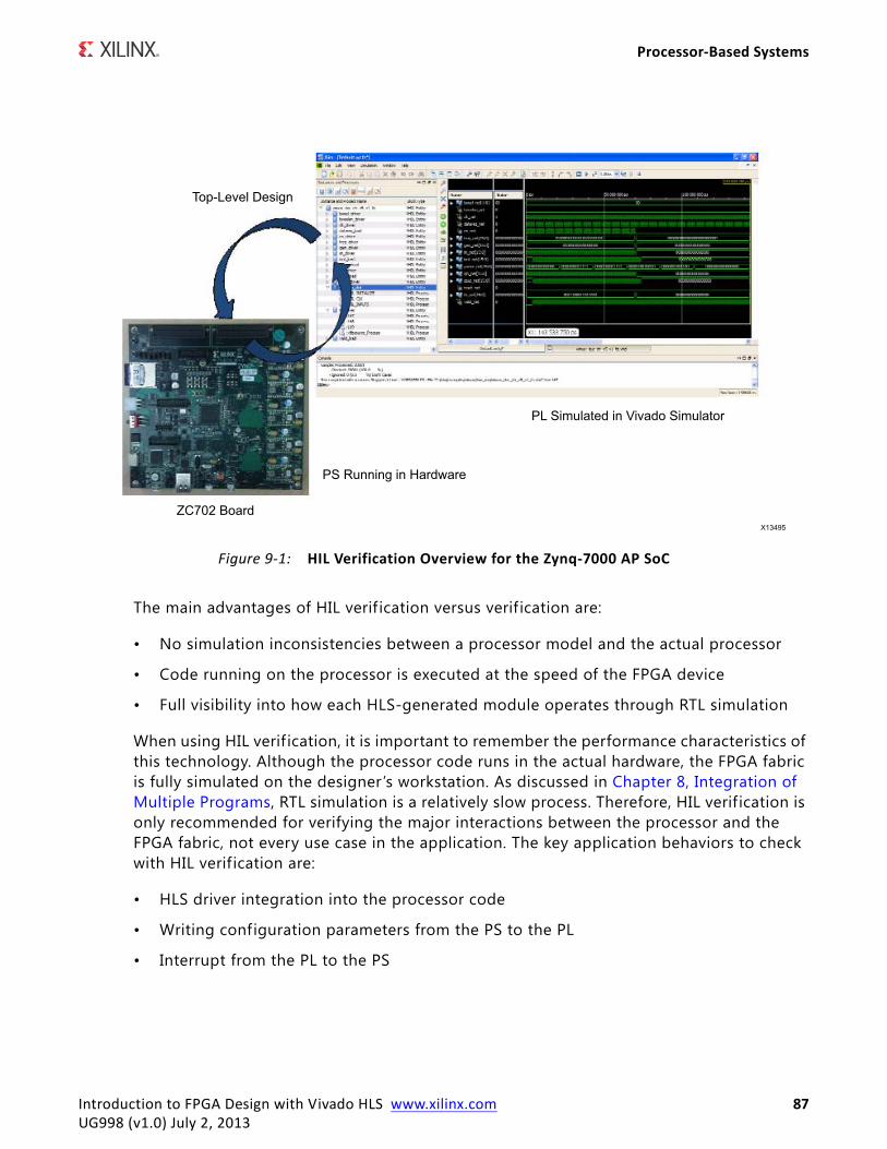
Processor-Based Systems
The main advantages of HIL verif ication versus verif ication are:
• No simulation inconsistencies between a processor model and the actual processor
• Code running on the processor is executed at the speed of the FPGA device
• Full visibility into how each HLS-generated module operates through RTL simulation
When using HIL verif ication, it is important to remember the performance characteristics of this technology. Although the processor code runs in the actual hardware, the FPGA fabric is fully simulated on the designer’s workstation. As discussed in Chapter 8, Integration of Multiple Programs, RTL simulation is a relatively slow process. Therefore, HIL verif ication is only recommended for verifying the major interactions between the processor and the FPGA fabric, not every use case in the application. The key application behaviors to check with HIL verif ication are:
• HLS driver integration into the processor code
• Writing configuration parameters from the PS to the PL
• Interrupt from the PL to the PS
X-Ref Target - Figure 9-1
Figure 9-1: HIL Verification Overview for the Zynq-7000 AP SoC
Introduction to FPGA Design with Vivado HLS www.xilinx.com 87UG998 (v1.0) July 2, 2013
Processor-Based Systems
Along with the RTL implementation of a software algorithm, the HLS compiler generates the software drivers needed for the processor to communicate with the generated hardware modules. The driver from HLS handles accelerator start and stop, configuration, and data transfer. This driver is available for both Linux and standalone software applications.
Note: A standalone software application is a system in which the processor only executes a single program and does not require OS support.
Virtual Platform VerificationVirtual platform technology is an established method of overlapping software and hardware development and is available for the Zynq-7000 AP SoC. A virtual platform is a software simulation of both the application and the hardware platform on which it runs. The models used for the PL portion of the design can be in C, C++, SystemC, or RTL. This simulation platform can be used as a proxy for the other recommended verif ication stages with varying degrees of f idelity to the hardware implementation.
In the fastest use case of the virtual platform, the application modules targeted to the PL are simulated from the C/C++ source code provided to the HLS compiler. This setup results in a functionally correct simulation that allows the designer to test the algorithm for correct computation. As modules are optimized and compiled with HLS, the generated RTL can replace the software version of the module to enable connectivity testing and timing driver simulation.
IMPORTANT: It is important to remember that adding RTL modules impacts the runtime on the virtual platform and slows down execution.
Device ValidationThe purpose of device validation is to check all the application use cases in which the processor interacts with the FPGA fabric. As in the case of standalone execution, this process involves running the complete application for a certain amount of time on the Zynq-7000 AP SoC. The purpose of this test is to check all the application corner cases with regard to the interaction between the PS and PL portions of the design.
Introduction to FPGA Design with Vivado HLS www.xilinx.com 88UG998 (v1.0) July 2, 2013
Introduction to FPGA Design with Vivado HLS www.xilinx.com 89UG998 (v1.0) July 2, 2013
Appendix A
Additional Resources
Xilinx ResourcesFor support resources such as Answers, Documentation, Downloads, and Forums, see the Xilinx Support website at:
www.xilinx.com/support.
For a glossary of technical terms used in Xilinx documentation, see:
www.xilinx.com/company/terms.htm.
Solution CentersSee the Xilinx Solution Centers for support on devices, software tools, and intellectual property at all stages of the design cycle. Topics include design assistance, advisories, and troubleshooting tips.
References1. Vivado® Design Suite User Guide: High-Level Synthesis (UG902)
2. AXI Reference Guide (UG761)
3. Vivado Design Suite User Guide: Designing with IP (UG896)
4. Vivado Design Suite User Guide: Designing IP Subsystems Using IP Integrator (UG994)
5. Vivado Design Suite Video Tutorials (www.xilinx.com/training/vivado/index.htm)
6. Vivado Design Suite Documentation (www.xilinx.com/support/index.html/content/xilinx/en/supportNav/design_tools/vivado_design_suite.html)