Embed Size (px)
Citation preview
XIAOYU HUAANCHAL GUPTA
Multi Threshold Technique for High Speed and Low Power Consumption
CMOS Circuits

Topics covered
IntroductionMethodologyFrameworkNew MTOF Flip Flop DesignConclusion

I. Introduction
Need for Low Power DesignReasons for Power Dissipation in flip-flopsHow to achieve it?MTCMOS

Need for Low Power Design
Limited battery capacity for handheld and portable devices.
Personal communication service devices requires more battery life and support high end data and signal processing– requires low power and high performance circuits
Saves energyMiniaturization of the circuit designIncreases circuit/system reliability Minimum heat dissipationMain drawback of current flip flop designs is the high
power consumption and high delay time
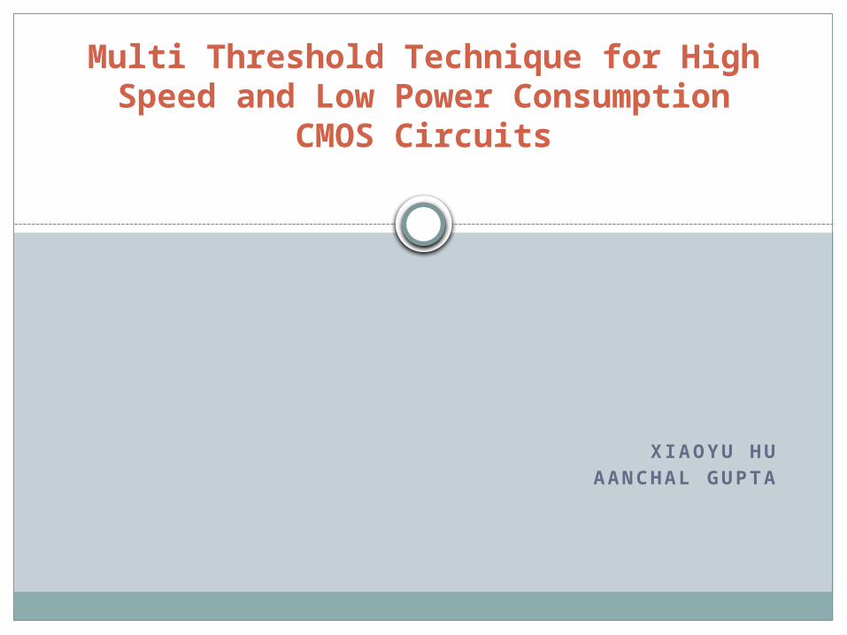
Reasons for Power Dissipation in flip-flops
Dynamic power—due to charging/discharging of gate capacitances with a change in input voltage Pdynamic = Cload*V2
DD*fclock
Td = Cload*VDD/(k(VDD-Vth)2
Reduce VDD and Vth Reducing VDD makes the speed of operation very sensitive
to the threshold voltage of transistor. But leakage current varies exponentially with Vth
Short circuit power Leakage power dissipation– Up to 40% of the
total power dissipation
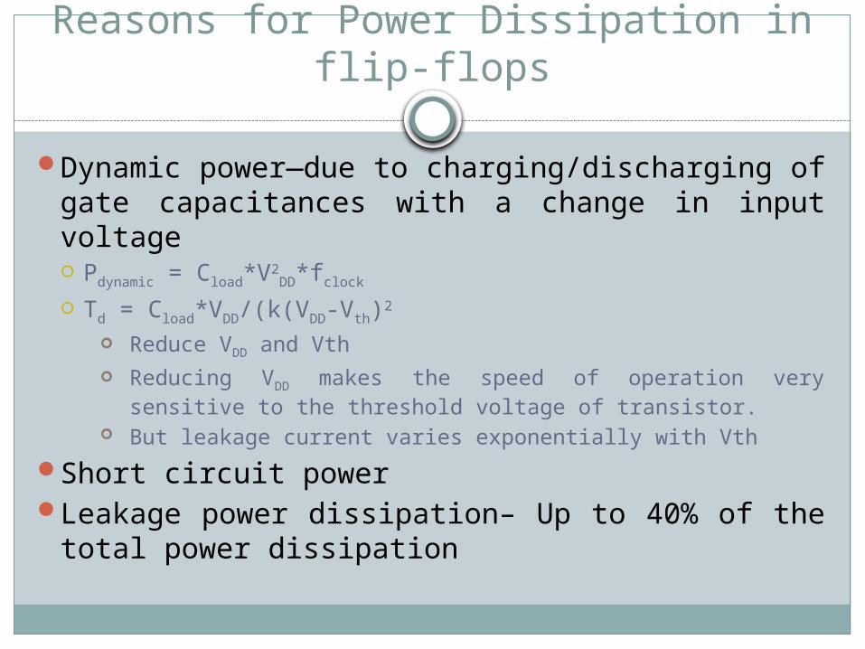
How to achieve it?
Reduce supply voltage.Reducing supply voltage degrades the speed
of operation.To support low power high speed operation
we need to reduce the threshold voltage of the transistors
Reducing Vth increases threshold current exponentially MTCMOS combines high Vth and low Vth
High Vth cuts off leakage current low Vth->reduces delay time, hence speed of operation is improved.
MTCMOS
Disconnects the low Vth logic gates from the power supply and ground lines by cutting off the high Vt sleep transistors whenever the circuit is idle
Sequential circuits loose their state during the sleep mode. A low leakage sleep mode with data retention capability
High threshold transistors have intrinsically low leakage and does not require gating transistors
II. Methodology
Power gatingClock gatingData retention circuitrySimulation SetupBlock diagram
Power Gating
Centralized power gating Advantageous considering the leakage paths are mutually exclusive Created virtual VDD and ground rails
Distributed power gating Simple to implement High area overhead Stack effect can degrade the performance More immune to ground bounce or voltage droop
Sleep control signal for maintaining and storing the circuit state during and after the sleep mode
The gating transistors are “on” during active mode and need to be wide enough to provide the required active current without significantly affecting performance.
Decide between fine and coarse granularity based on the circuit to avoid leakage paths If isolated circuitry is used for data storage—coarse granularity
Clock Gating
Masks the clock signal when the circuit is not performing useful computation
Use an enable signal to control the clock signal during the sleep mode.
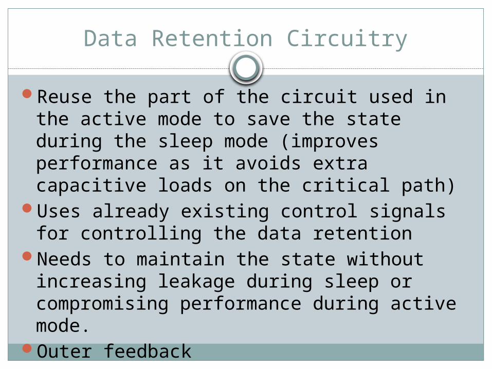
Data Retention Circuitry
Reuse the part of the circuit used in the active mode to save the state during the sleep mode (improves performance as it avoids extra capacitive loads on the critical path)
Uses already existing control signals for controlling the data retention
Needs to maintain the state without increasing leakage during sleep or compromising performance during active mode.
Outer feedback
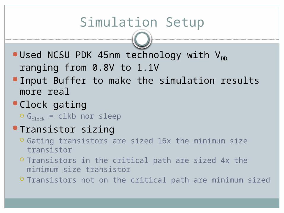
Simulation Setup
Used NCSU PDK 45nm technology with VDD ranging from 0.8V to 1.1V
Input Buffer to make the simulation results more real
Clock gating Gclock = clkb nor sleep
Transistor sizing Gating transistors are sized 16x the minimum size
transistor Transistors in the critical path are sized 4x the minimum
size transistor Transistors not on the critical path are minimum sized
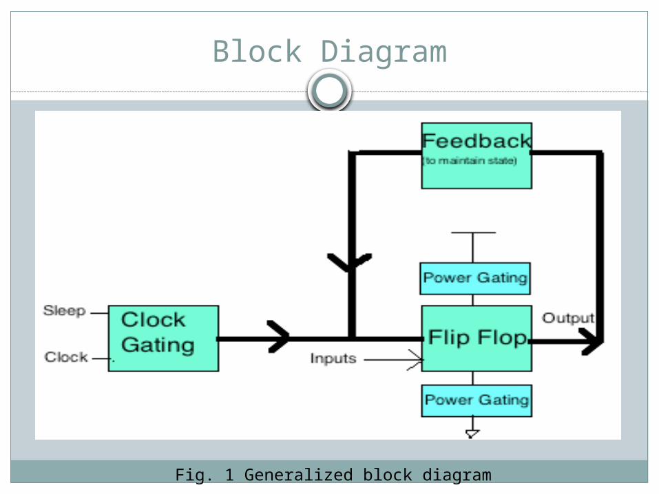
Block Diagram
Fig. 1 Generalized block diagram
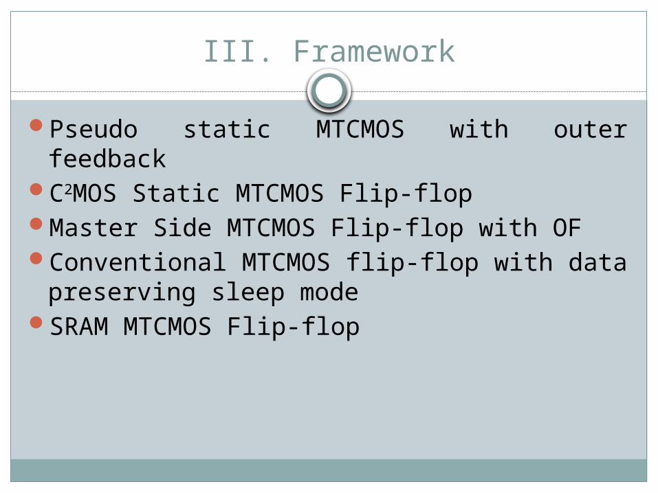
III. Framework
Pseudo static MTCMOS with outer feedbackC2MOS Static MTCMOS Flip-flopMaster Side MTCMOS Flip-flop with OFConventional MTCMOS flip-flop with data
preserving sleep modeSRAM MTCMOS Flip-flop
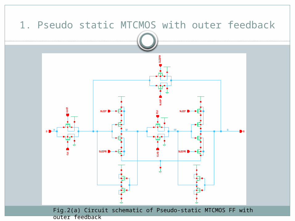
1. Pseudo static MTCMOS with outer feedback
Fig.2(a) Circuit schematic of Pseudo-static MTCMOS FF with outer feedback
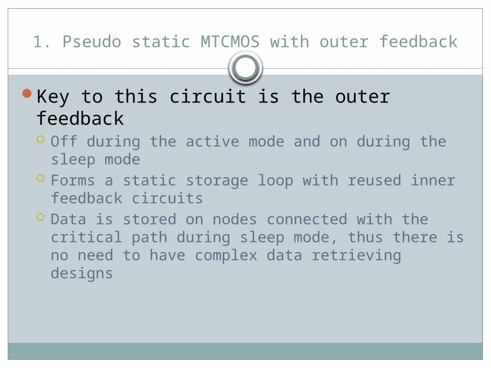
1. Pseudo static MTCMOS with outer feedback
Key to this circuit is the outer feedback Off during the active mode and on during the sleep
mode Forms a static storage loop with reused inner
feedback circuits Data is stored on nodes connected with the critical
path during sleep mode, thus there is no need to have complex data retrieving designs
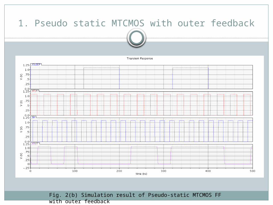
1. Pseudo static MTCMOS with outer feedback
Fig. 2(b) Simulation result of Pseudo-static MTCMOS FF with outer feedback
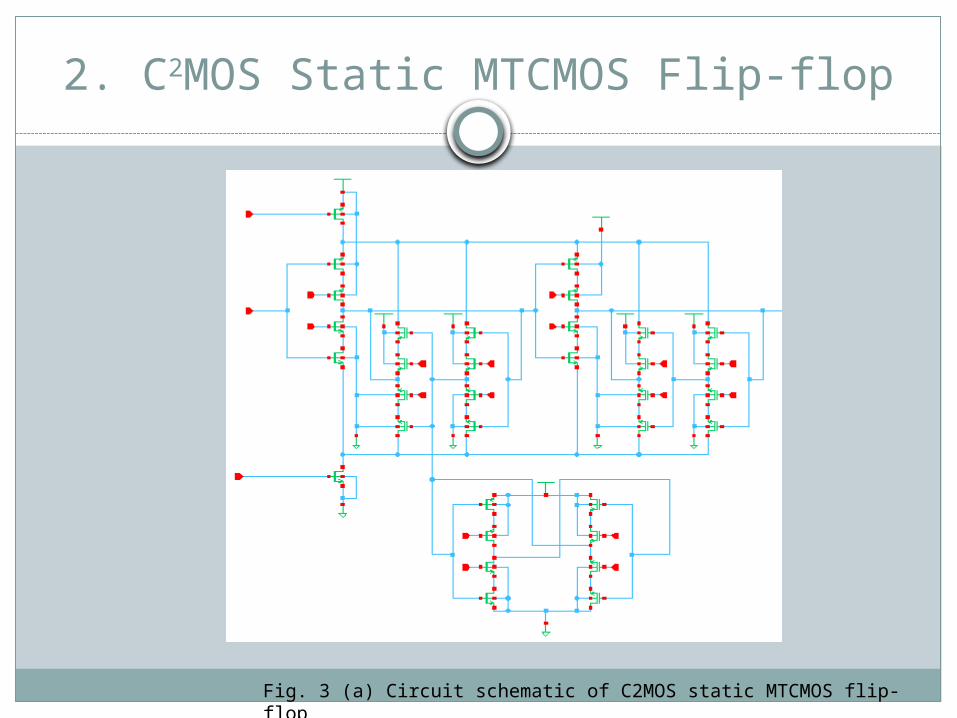
2. C2MOS Static MTCMOS Flip-flop
Fig. 3 (a) Circuit schematic of C2MOS static MTCMOS flip-flop
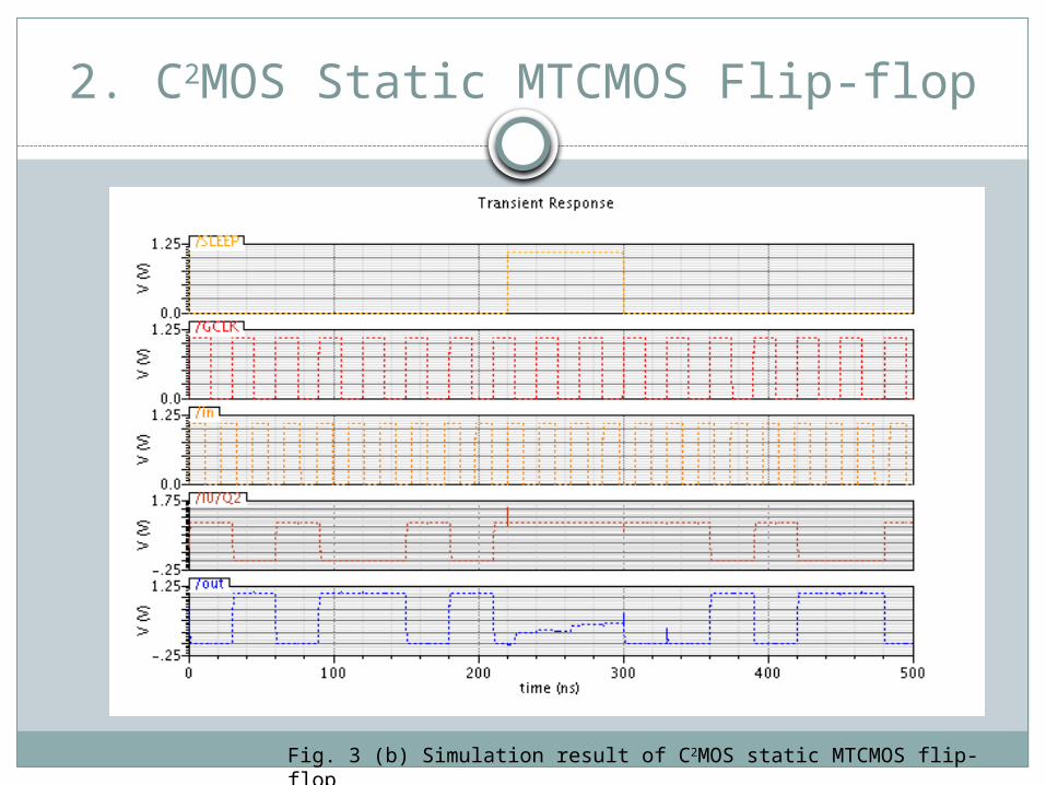
2. C2MOS Static MTCMOS Flip-flop
Fig. 3 (b) Simulation result of C2MOS static MTCMOS flip-flop
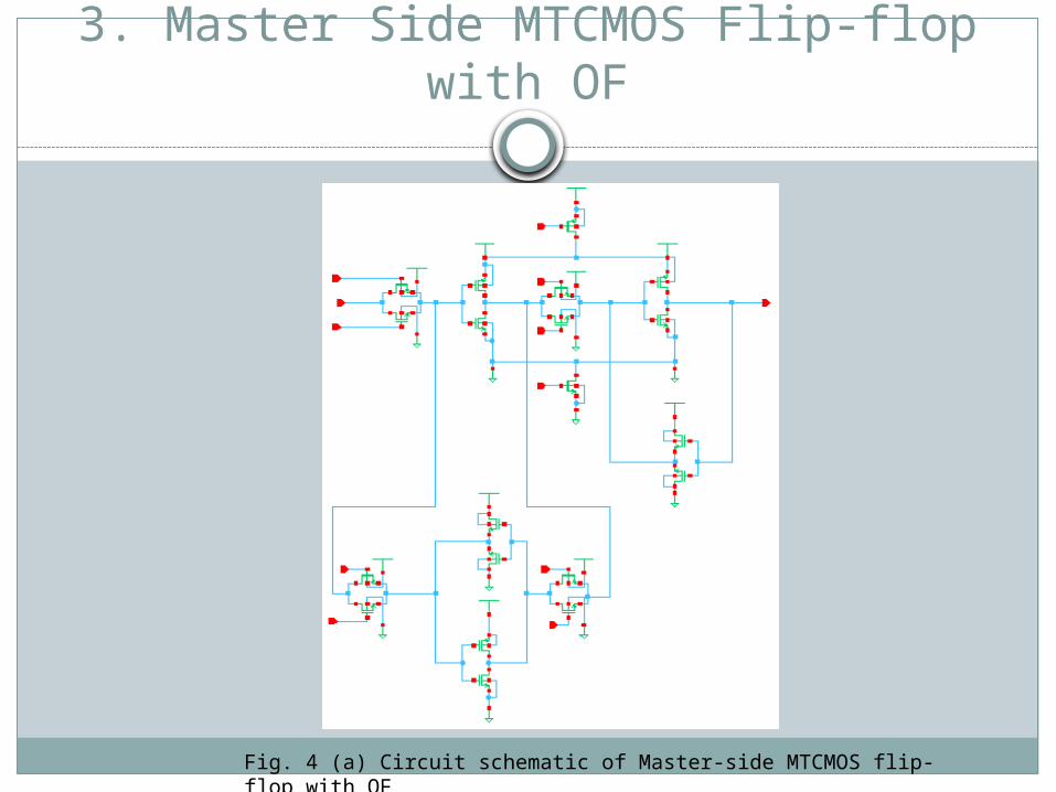
3. Master Side MTCMOS Flip-flop with OF
Fig. 4 (a) Circuit schematic of Master-side MTCMOS flip-flop with OF
3. Master Side MTCMOS Flip-flop with OF
Uses separate nodes for storing the state during the sleep mode.
Critical path isolated from the outer feedback loop.
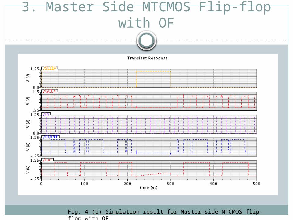
3. Master Side MTCMOS Flip-flop with OF
Fig. 4 (b) Simulation result for Master-side MTCMOS flip-flop with OF

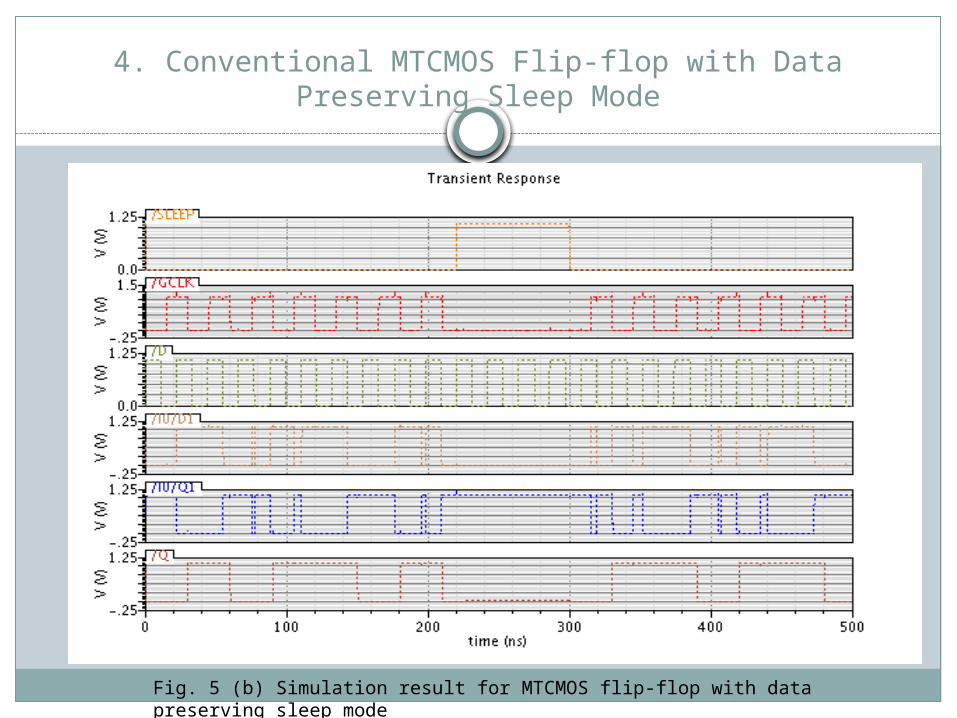
4. Conventional MTCMOS flip-flop with data preserving sleep mode
Fig. 5 (a) Circuit schematic of MTCMOS flip-flop with data preserving sleep mode
4. Conventional MTCMOS Flip-flop with Data Preserving Sleep Mode
Fig. 5 (b) Simulation result for MTCMOS flip-flop with data preserving sleep mode
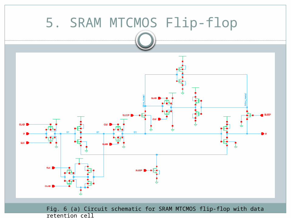
5. SRAM MTCMOS Flip-flop
Fig. 6 (a) Circuit schematic for SRAM MTCMOS flip-flop with data retention cell
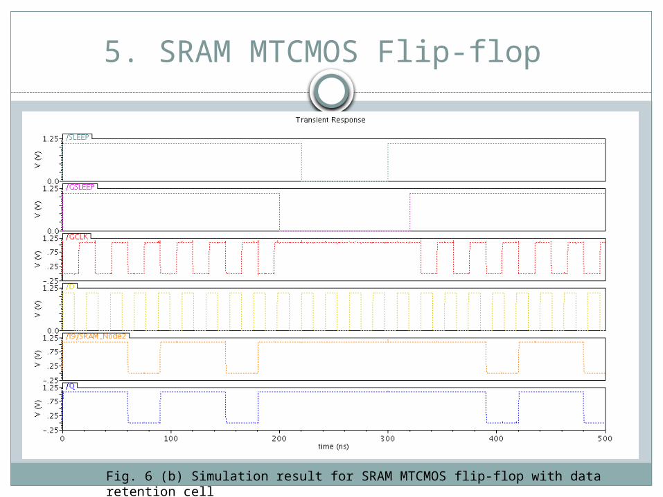
5. SRAM MTCMOS Flip-flop
Fig. 6 (b) Simulation result for SRAM MTCMOS flip-flop with data retention cell
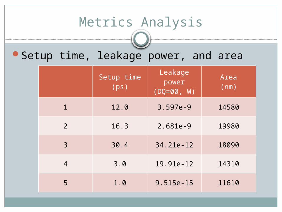
Metrics Analysis
Setup time, leakage power, and area
Setup time(ps)
Leakage power
(DQ=00, W)
Area(nm)
1 12.0 3.597e-9 14580
2 16.3 2.681e-9 19980
3 30.4 34.21e-12 18090
4 3.0 19.91e-12 14310
5 1.0 9.515e-15 11610
Metrics Analysis
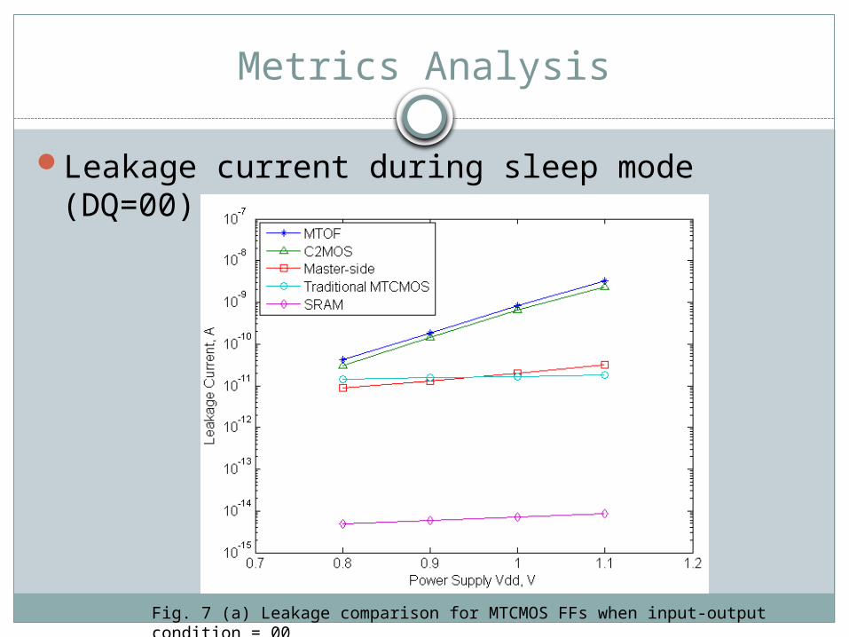
Leakage current during sleep mode (DQ=00)
Fig. 7 (a) Leakage comparison for MTCMOS FFs when input-output condition = 00
Metrics Analysis
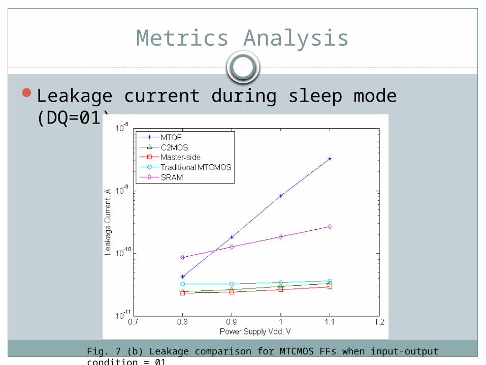
Leakage current during sleep mode (DQ=01)
Fig. 7 (b) Leakage comparison for MTCMOS FFs when input-output condition = 01
Metrics Analysis
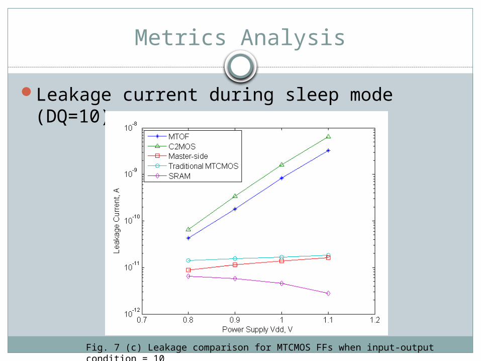
Leakage current during sleep mode (DQ=10)
Fig. 7 (c) Leakage comparison for MTCMOS FFs when input-output condition = 10
Metrics Analysis
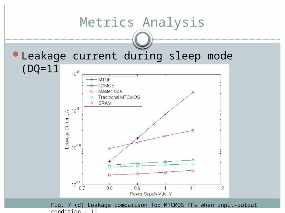
Leakage current during sleep mode (DQ=11)
Fig. 7 (d) Leakage comparison for MTCMOS FFs when input-output condition = 11

New MTOF Flip-flop Design
Rising-edge MTCMOS FF with Slave-side Outer Feedback Design 1
Rising-edge MTCMOS FF with Slave-side Outer Feedback Design 2 Schematic Logic function simulation Metrics analysis
Rising-edge MTCMOS FF with Slave-side OF Design 1
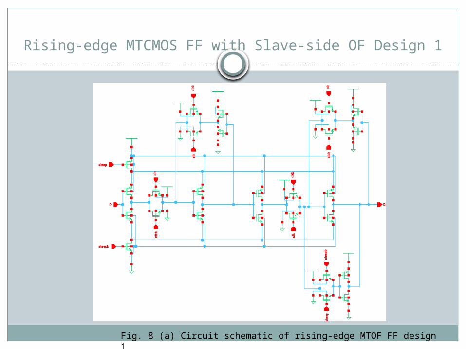
Fig. 8 (a) Circuit schematic of rising-edge MTOF FF design 1
Rising-edge MTCMOS FF with Slave-side OF Design 1
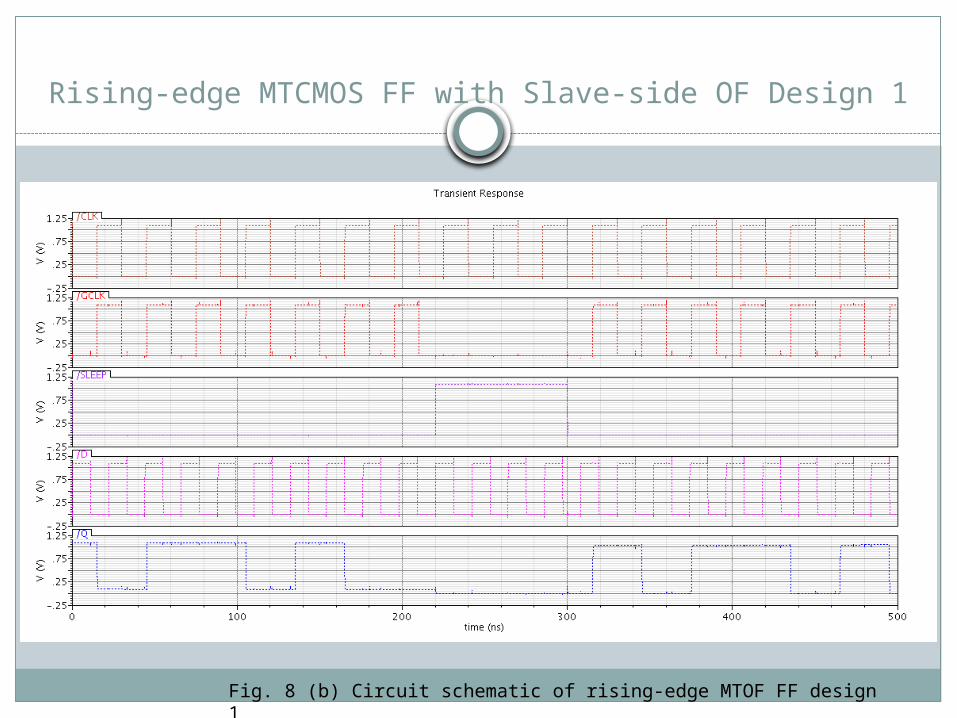
Fig. 8 (b) Circuit schematic of rising-edge MTOF FF design 1
Rising-edge MTCMOS FF with Slave-side OF Design 1
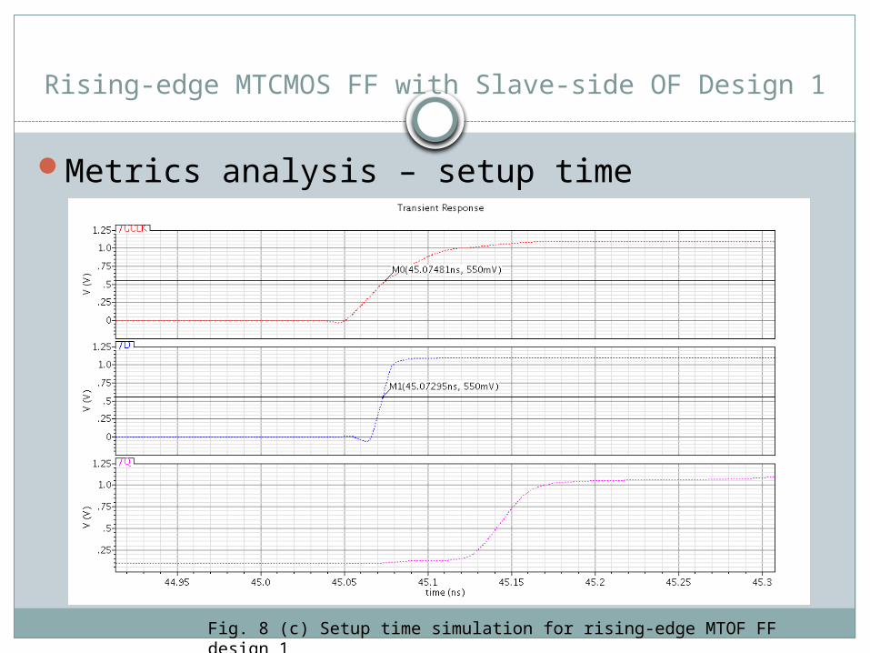
Fig. 8 (c) Setup time simulation for rising-edge MTOF FF design 1
Metrics analysis – setup time
Rising-edge MTCMOS FF with Slave-side OF Design 1
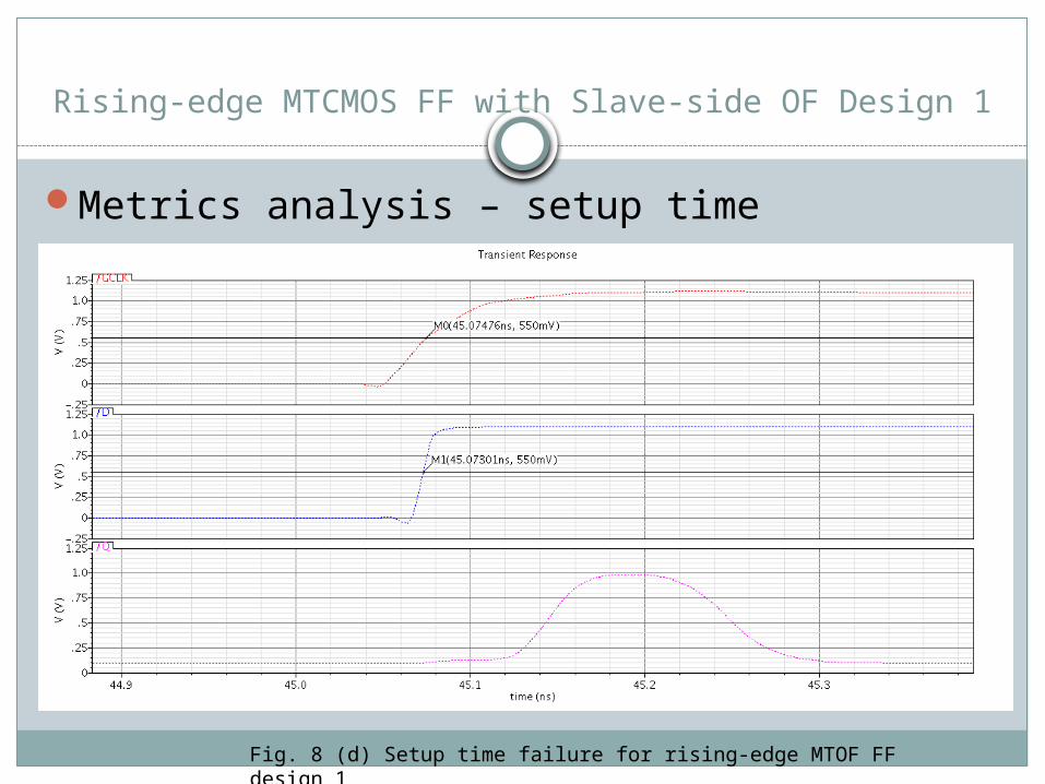
Fig. 8 (d) Setup time failure for rising-edge MTOF FF design 1
Metrics analysis – setup time
Rising-edge MTCMOS FF with Slave-side OF Design 1
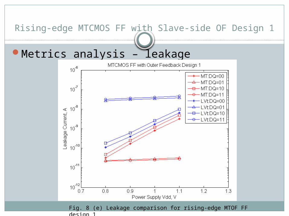
Fig. 8 (e) Leakage comparison for rising-edge MTOF FF design 1
Metrics analysis – leakage
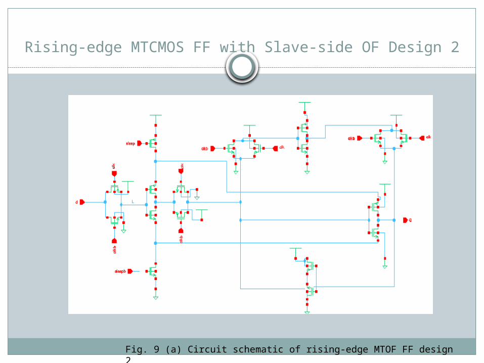
Rising-edge MTCMOS FF with Slave-side OF Design 2
Fig. 9 (a) Circuit schematic of rising-edge MTOF FF design 2
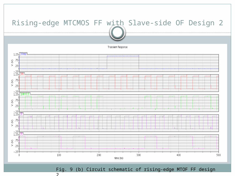
Rising-edge MTCMOS FF with Slave-side OF Design 2
Fig. 9 (b) Circuit schematic of rising-edge MTOF FF design 2
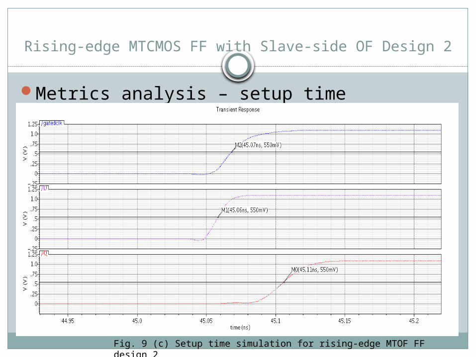
Rising-edge MTCMOS FF with Slave-side OF Design 2
Fig. 9 (c) Setup time simulation for rising-edge MTOF FF design 2
Metrics analysis – setup time
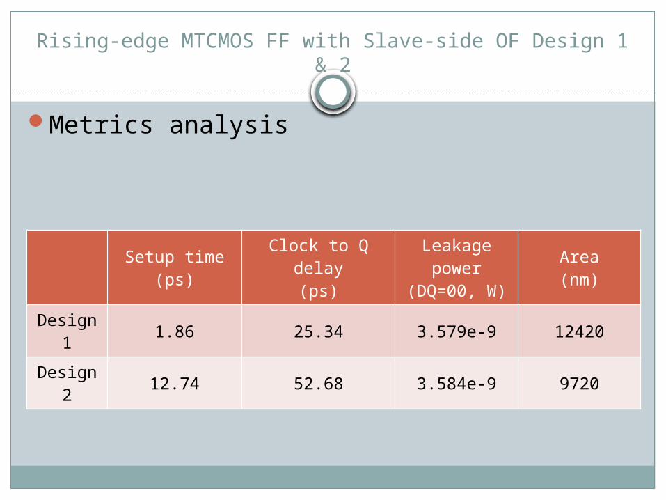
Rising-edge MTCMOS FF with Slave-side OF Design 1 & 2
Metrics analysis
Setup time(ps)
Clock to Q delay(ps)
Leakage power
(DQ=00, W)
Area(nm)
Design 1 1.86 25.34 3.579e-9 12420
Design 2 12.74 52.68 3.584e-9 9720
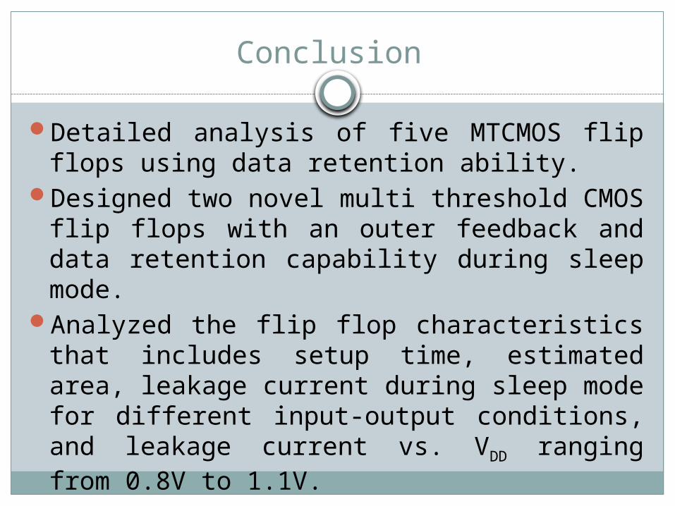
Conclusion
Detailed analysis of five MTCMOS flip flops using data retention ability.
Designed two novel multi threshold CMOS flip flops with an outer feedback and data retention capability during sleep mode.
Analyzed the flip flop characteristics that includes setup time, estimated area, leakage current during sleep mode for different input-output conditions, and leakage current vs. VDD ranging from 0.8V to 1.1V.