Embed Size (px)
Citation preview

1/26
XCL210 Series 50mA/200mA Inductor Built-in Step-Down “micro DC/DC” Converters
0
20
40
60
80
100
0.01 0.1 1 10 100
Effi
cien
cy :
EFF
I [%
]
Output Current : IOUT [mA]
VIN=3.6VVIN=4.2V
ETR28009-002
GENERAL DESCRIPTION
The XCL210 series is a synchronous step-down micro DC/DC converter which integrates an inductor and a control IC in one tiny package (2.0mm×2.5mm, h=1.0mm). An internal coil simplifies the circuit and enables minimization of noise and other operational trouble due to the circuit wiring. A wide operating voltage range of 2.0V to 6.0V enables support for applications that require an internally fixed output voltage from 1.0V to 4.0V(Type A/B/C/D), 0.6V to 0.95V(Type F/H) in increments of 0.05V. During stand-by, all circuits are shutdown to reduce currentconsumption to as low as 0.1μA or less. With the built-in UVLO (Under Voltage Lock Out) function, the internal P-channel MOS driver transistor is forced OFF when input voltage becomes UVLO ditect Voltage or lower. The XCL210 integrate CL discharge function which enables the electric charge at the output capacitor CL to be discharged via the internal discharge switch located between the LX and VSS pins. When the devices enter stand-by mode, output voltage quickly returns to the VSS level as a result of this function.
FEATURESInput Voltage : 2.0V~6.0V
Output Voltage : 1.0V~4.0V (±2.0%, Type A/B/C/D) 0.6V~0.95V (±2.0%, Type F/H) Control Methods : PFM control Output Current : 200mA(Type A/C) 50mA(Type B/D/F/H) Supply Current : 0.5μA High Efficiency : 93% (VIN=3.6V,VOUT=3.0V/100μA) Function : UVLO Short Circuit Protection CL Discharge(Type C/D/H) Capacitor : Low ESR Ceramic Capacitor Operating Ambient Temperature : -40 ~ +85
Packages : CL-2025-02 Environmentally Friendly : EU RoHS Compliant, Pb Free
TYPICAL PERFORMANCECHARACTERISTICS
TYPICAL APPLICATION CIRCUIT
GreenOperationCompatible
50mA
CIN
10μFCL
22μF
7
8
1
2
3 4
5
6
GND
VINLx
CEVOUT
NC
VIN
APPLICATIONS Wearable Devices
Smart meters
Bluetooth units
Energy Harvest devices
Back up power supply circuits
Portable game consoles
Devices with 1 Lithium cell
XCL210B301GR-G(VOUT=3.0V)

2/26
XCL210 Series BLOCK DIAGRAM
XCL210 Series, Type A/Type B/Type F
* XCL210A and B and F type do not have CL Discharge function. * Diodes inside the circuits are ESD protection diodes and parasitic diodes.
XCL210 Series, Type C/Type D/Type H
* Diodes inside the circuits are ESD protection diodes and parasitic diodes.
Lx
Inductor
GND
L2 L1
VIN
VOUT
CE
PFM Comparator
R2
R1
SynchBufferDrive
PFMController
Vref
ShortProtection
CFB
CurrentSense
UVLOVIN Start Up
Controller
CE Controller Logic
VDD
VDD
Lx
Inductor
GND
L2 L1
VIN
VOUT
CE
PFM Comparator
R2
R1
SynchBufferDrive
PFMController
Vref
ShortProtection
CFB
CurrentSenseCL
Discharge
UVLOVIN Start Up
Controller
CE Controller Logic
VDD
VDD

3/26
XCL210Series
PRODUCT CLASSIFICATION
Ordering information(Type A/B/C/D) XCL210①②③④⑤⑥-⑦ PFM control
Ordering information(Type F/H) XCL210①②③④⑤⑥-⑦ PFM control
DESIGNATOR ITEM SYMBOL DESCRIPTION
① Product Type
A IOUT=200mA , Without CL Auto Discharge B IOUT=50mA Without CL Auto Discharge C IOUT=200mA , With CL Auto Discharge D IOUT=50mA, With CL Auto Discharge
②③ Output Voltage 10~40
Output voltage options e.g.) 1.2V → ② = 1 ③ = 2 1.25V→ ② = 1 ③ = C 0.05V increments : 0.05=A, 0.15=B, 0.25=C, 0.35=D, 0.45=E, 0.55=F, 0.65=H, 0.75=K, 0.85=L, 0.95=M
④ Fixed number 1 Fixed number
⑤⑥-⑦(*1) Package (Order Unit) GR-G CL-2025-02 (3,000pcs/Reel)
DESIGNATOR ITEM SYMBOL DESCRIPTION
① Product Type F IOUT=50mA , Without CL Auto Discharge H IOUT=50mA , With CL Auto Discharge
②③ Output Voltage 06~0M
Output voltage options e.g.) 0.6V → ② = 0 ③ = 6 0.95V→ ② = 0 ③ = M 0.05V increments : 0.65=H, 0.75=K, 0.85=L, 0.95=M
④ Fixed number 1 Fixed number
⑤⑥-⑦(*1) Package (Order Unit) GR-G CL-2025-02 (3,000pcs/Reel)
(*1) The “-G” suffix denotes Halogen and Antimony free as well as being fully EU RoHS compliant.
(*1) The “-G” suffix denotes Halogen and Antimony free as well as being fully EU RoHS compliant.

4/26
XCL210 Series PIN CONFIGURATION
PIN ASSIGNMENT PIN NUMBER PIN NAME FUNCTIONS
1 LX Switching 2 GND Ground 3 VOUT Output Voltage 4 CE Chip Enable 5 NC No Connection 6 VIN Power Input 7 L1 Inductor Electrodes 8 L2 Inductor Electrodes
CE PIN FUNCTION PIN NAME SIGNAL STATUS
CE H Operation (All Types) L Standby (All Types)
* Please do not leave the CE pin open.
ABSOLUTE MAXIMUM RATINGS Ta=25˚C
PARAMETER SYMBOL RATINGS UNITS
VIN Pin Voltage VIN -0.3 ~ +7.0 V LX Pin Voltage VLX -0.3 ~ VIN+0.3 or +7.0 (*1) V
VOUT Pin Voltage VOUT -0.3 ~ VIN+0.3 or +7.0 (*1) V CE Pin Voltage VCE -0.3 ~ +7.0 V
LX Pin Current ILX 1000 mA
Power Dissipation Pd 1000(*2) mW Operating Ambient Temperature Topr -40 ~ +85 ˚C
Storage Temperature Tstg -55 ~ +125 ˚C * All voltages are described based on the GND.
(*1) The maximum value is the lower of either VIN + 0.3 or +7.0. (*2) The power dissipation figure shown is PCB mounted (40mm×40mm, t=1.6mm, Glass Epoxy FR-4).
Please refer to page 15 for details.
(BOTTOM VIEW)
L1
L2
7
8
VIN 6
NC 5
CE 4
1 Lx
2 GND
3 VOUT
* The dissipation pad for the CL-2025-02 package should be solder-plated in recommended mount pattern and metal masking so as to enhance mounting strength and heat release. The mount pattern should be connected to GND pin (No.2).

5/26
XCL210Series
ELECTRICAL CHARACTERISTICS XCL210Axx1GR-G, without CL discharge function
PARAMETER SYMBOL CONDITIONS MIN. TYP. MAX. UNITS CIRCUIT
Input Voltage VIN - 2.0 - 6.0 V ①
Output Voltage VOUT(E) (*2) Resistor connected with LX pin. Voltage which LX pin
changes “L” to “H” level while VOUT is decreasing. E1 V ②
UVLO Release Voltage VUVLO(E) VCE=VIN, VOUT=0V. Resistor connected with LX pin. Voltage which LX pin changes “L” to “H” level while VIN is increasing.
1.65 1.80 1.95 V ②
UVLO Hysteresis Voltage
VHYS(E) VCE=VIN, VOUT=0V. Resistor connected with LX pin. VUVLO(E) - Voltage which LX pin changes “H” to “L” level while VIN is decreasing.
0.11 0.15 0.24 V ②
Supply Current Iq VIN=VCE=VOUT(T)+0.5V (*1), VIN=2.0V, if VOUT(T)≦1.5V (*1), VOUT=VOUT(T)+0.5V (*1), LX=Open.
E2 μA ③
Standby Current ISTB VIN=5.0V, VCE=VOUT=0V, LX=Open. - 0.1 1.0 μA ③ LX SW “H” Leak
Current ILEAKH VIN=5.0V, VCE=VOUT=0V, VLX=0V. - 0.1 1.0 μA ③
LX SW “L” Leak Current ILEAKL VIN=5.0V, VCE=VOUT=0V, VLX=5.0V. - 0.1 1.0 μA ③
PFM Switching Current IPFM VIN=VCE=VOUT(T)+2.0V (*1), IOUT=10mA. 260 330 400 mA ①
Maximum Duty Ratio (*3)
MAXDTYVIN=VOUT=VOUT(T)×0.95V(*1), VCE=1.2V Resistor connected with LX pin.
100 - - % ②
Efficiency (*4) EFFI VIN=VCE=5.0V, VOUT(T)=4.0V (*1), IOUT=30mA. - 93 - % ⑥ Efficiency (*4) EFFI VIN=VCE=3.6V, VOUT(T)=3.3V (*1), IOUT=30mA. - 93 - % ⑥ Efficiency (*4) EFFI VIN=VCE=3.6V, VOUT(T)=1.8V (*1), IOUT=30mA. - 87 - % ⑥ LX SW “Pch”
ON Resistance (*5) RLXP VIN=VCE=5.0V, VOUT=0V, ILX=100mA. - 0.4 0.65 Ω ④
LX SW “Nch” ON Resistance
RLXN VIN=VCE=5.0V. - 0.4 (*6) - Ω -
Output Voltage Temperature
Characteristics
∆VOUT/ (VOUT・∆Topr)
-40≦Topr≦85. - ±100 - ppm/ ②
CE “High” Voltage VCEH VOUT=0V. Resistor connected with LX pin. Voltage which LX pin changes “L” to “H” level while VCE=0.2→1.5V.
1.2 - 6.0 V ⑤
CE “Low” Voltage VCEL VOUT=0V. Resistor connected with LX pin. Voltage which LX pin changes “H” to “L” level while VCE=1.5→0.2V.
GND - 0.3 V ⑤
CE “High” Current ICEH VIN=VCE=5.0V, VOUT=0V, LX=Open. -0.1 - 0.1 μA ⑤ CE “Low” Current ICEL VIN=5.0V, VCE=VOUT=0V, LX=Open. -0.1 - 0.1 μA ⑤
Short Protection Threshold Voltage
VSHORT Resistor connected with LX pin. Voltage which LX pin changes “H” to “L” level while VOUT= VOUT(T)+0.1V→0V(*1).
0.4 0.5 0.6 V ②
Inductance Value L Test Frequency=1MHz - 8.0 - μH
Inductor Rated Current IDC_L ∆T=+40 - 600 - mA
Unless otherwise stated, VIN=VCE=5.0V (*1) VOUT(T)=Nominal Output Voltage (*2) VOUT(E)=Effective Output Voltage The actual output voltage value VOUT(E) is the PFM comparator threshold voltage in the IC. Therefore, the DC/DC circuit output voltage, including the peripheral components, is boosted by the ripple voltage average value. Please refer to the characteristic example. (*3) Not applicable to the products with VOUT(T) < 2.15V since it is out of operational volatge range. (*4) EFFI=[ (Output Voltage)×(Output Current)] / [(Input Voltage)×(Input Current)]×100 (*5) LX SW “Pch” ON resistance = (VIN – VLX pin measurement voltage) / 100mA (*6) Designed value
Ta=25˚C

6/26
XCL210 Series ELECTRICAL CHARACTERISTICS (Continued) XCL210Bxx1GR-G, without CL discharge function
PARAMETER SYMBOL CONDITIONS MIN. TYP. MAX. UNITS CIRCUIT
Input Voltage VIN - 2.0 - 6.0 V ①
Output Voltage VOUT(E) (*2) Resistor connected with LX pin.Voltage which LX pin
changes “L” to “H” level while VOUT is decreasing. E1 V ②
UVLO Release Voltage VUVLO(E) VCE=VIN, VOUT=0V. Resistor connected with LX pin. Voltage which LX pin changes “L” to “H” level while VIN is increasing.
1.65 1.80 1.95 V ②
UVLO Hysteresis Voltage
VHYS(E) VCE=VIN, VOUT=0V. Resistor connected with LX pin. VUVLO(E) - Voltage which LX pin changes “H” to “L” level while VIN is decreasing.
0.11 0.15 0.24 V ②
Supply Current Iq VIN=VCE=VOUT(T)+0.5V (*1),VIN=2.0V, if VOUT(T)≦1.5V (*1), VOUT=VOUT(T)+0.5V (*1), LX=Open.
E2 μA ③
Standby Current ISTB VIN=5.0V, VCE=VOUT=0V, LX=Open. - 0.1 1.0 μA ③ LX SW “H” Leak
Current ILEAKH VIN=5.0V, VCE=VOUT=0V, VLX=0V. - 0.1 1.0 μA ③
LX SW “L” Leak Current ILEAKL VIN=5.0V, VCE=VOUT=0V, VLX=5.0V. - 0.1 1.0 μA ③
PFM Switching Current IPFM VIN=VCE=VOUT(T)+2.0V (*1), IOUT=10mA. 115 180 250 mA ①
Maximum Duty Ratio (*3)
MAXDTYVIN=VOUT=VOUT(T)×0.95V(*1), VCE=1.2V Resistor connected with LX pin.
100 - - % ②
Efficiency (*4) EFFI VIN=VCE=5.0V,VOUT(T)=4.0V (*1), IOUT=30mA. - 95 - % ⑥ Efficiency (*4) EFFI VIN=VCE=3.6V, VOUT(T)=3.3V (*1), IOUT=30mA. - 95 - % ⑥ Efficiency (*4) EFFI VIN=VCE=3.6V, VOUT(T)=1.8V (*1), IOUT=30mA. - 89 - % ⑥ LX SW “Pch”
ON Resistance (*5) RLXP VIN=VCE=5.0V, VOUT=0V, ILX=100mA. - 0.4 0.65 Ω ④
LX SW “Nch” ON Resistance
RLXN VIN=VCE=5.0V. - 0.4 (*6) - Ω -
Output Voltage Temperature
Characteristics
∆VOUT/ (VOUT・∆Topr)
-40≦Topr≦85. - ±100 - ppm/ ②
CE “High” Voltage VCEH VOUT=0V. Resistor connected with LX pin. Voltage which LX pin changes “L” to “H” level while VCE=0.2→1.5V.
1.2 - 6.0 V ⑤
CE “Low” Voltage VCEL VOUT=0V. Resistor connected with LX pin. Voltage which LX pin changes “H” to “L” level while VCE=1.5→0.2V.
GND - 0.3 V ⑤
CE “High” Current ICEH VIN=VCE=5.0V, VOUT=0V, LX=Open. -0.1 - 0.1 μA ⑤ CE “Low” Current ICEL VIN=5.0V, VCE=VOUT=0V, LX=Open. -0.1 - 0.1 μA ⑤
Short Protection Threshold Voltage
VSHORT Resistor connected with LX pin. Voltage which LX pin changes “H” to “L” level while VOUT=VOUT(T)+0.1V→0V(*1).
0.4 0.5 0.6 V ②
Inductance Value L Test Frequency=1MHz - 8.0 - μH Inductor Rated Current IDC_L ∆T=+40 - 600 - mA
Unless otherwise stated, VIN=VCE=5.0V (*1) VOUT(T)=Nominal Output Voltage (*2) VOUT(E)=Effective Output Voltage The actual output voltage value VOUT(E) is the PFM comparator threshold voltage in the IC. Therefore, the DC/DC circuit output voltage, including the peripheral components, is boosted by the ripple voltage average value. Please refer to the characteristic example. (*3) Not applicable to the products with VOUT(T) < 2.15V since it is out of operational volatge range. (*4) EFFI=[ (Output Voltage)×(Output Current)] / [(Input Voltage)×(Input Current)]×100 (*5) LX SW “Pch” ON resistance = (VIN – VLX pin measurement voltage) / 100mA (*6) Designed value
Ta=25˚CTa=25˚C

7/26
XCL210Series
ELECTRICAL CHARACTERISTICS (Continued) XCL210Cxx1GR-G, with CL Discharge Function
PARAMETER SYMBOL CONDITIONS MIN. TYP. MAX. UNITS CIRCUIT
Input Voltage VIN - 2.0 - 6.0 V ①
Output Voltage VOUT(E) (*2) Resistor connected with LX pin. Voltage which LX pin
changes “L” to “H” level while VOUT is decreasing. E1 V ②
UVLO Release Voltage VUVLO(E) VCE=VIN, VOUT=0V. Resistor connected with LX pin. Voltage which LX pin changes “L” to “H” level while VIN is increasing.
1.65 1.80 1.95 V ②
UVLO Hysteresis Voltage
VHYS(E) VCE=VIN, VOUT=0V. Resistor connected with LX pin. VUVLO(E) - Voltage which LX pin changes “H” to “L” level while VIN is decreasing.
0.11 0.15 0.24 V ②
Supply Current Iq VIN=VCE=VOUT(T)+0.5V (*1),VIN=2.0V, if VOUT(T)≦1.5V (*1),
VOUT=VOUT(T)+0.5V (*1), LX=Open. E2 μA ③
Standby Current ISTB VIN=5.0V, VCE=VOUT=0V, LX=Open. - 0.1 1.0 μA ③ LX SW “H” Leak
Current ILEAKH VIN=5.0V, VCE=VOUT=0V, VLX=0V. - 0.1 1.0 μA ③
LX SW “L” Leak Current ILEAKL VIN=5.0V, VCE=VOUT=0V, VLX=5.0V. - 0.1 1.0 μA ③
PFM Switching Current IPFM VIN=VCE=VOUT(T)+2.0V (*1), IOUT=10mA. 260 330 400 mA ①
Maximum Duty Ratio (*3)
MAXDTYVIN=VOUT=VOUT(T)×0.95V(*1), VCE=1.2V Resistor connected with LX pin.
100 - - % ②
Efficiency (*4) EFFI VIN=VCE=5.0V, VOUT(T)=4.0V (*1), IOUT=30mA. - 93 - % ⑥ Efficiency (*4) EFFI VIN=VCE=3.6V, VOUT(T)=3.3V (*1), IOUT=30mA. - 93 - % ⑥ Efficiency (*4) EFFI VIN=VCE=3.6V, VOUT(T)=1.8V (*1), IOUT=30mA. - 87 - % ⑥ LX SW “Pch”
ON Resistance (*5) RLXP VIN=VCE=5.0V, VOUT=0V, ILX=100mA. - 0.4 0.65 Ω ④
LX SW “Nch” ON Resistance
RLXN VIN=VCE=5.0V. - 0.4 (*6) - Ω -
Output Voltage Temperature
Characteristics
∆VOUT/ (VOUT・∆Topr)
-40≦Topr≦85. - ±100 - ppm/ ②
CE “High” Voltage VCEH VOUT=0V. Resistor connected with LX pin. Voltage which LX pin changes “L” to “H” level while VCE=0.2→1.5V.
1.2 - 6.0 V ⑤
CE “Low” Voltage VCEL VOUT=0V. Resistor connected with LX pin. Voltage which LX pin changes “H” to “L” level while VCE=1.5→0.2V.
GND - 0.3 V ⑤
CE “High” Current ICEH VIN=VCE=5.0V, VOUT=0V, LX=Open. -0.1 - 0.1 μA ⑤ CE “Low” Current ICEL VIN=5.0V, VCE=VOUT=0V, LX=Open. -0.1 - 0.1 μA ⑤
Short Protection Threshold Voltage
VSHORT Resistor connected with LX pin. Voltage which LX pin changes “H” to “L” level while VOUT= VOUT(T)+0.1V→0V(*1).
0.4 0.5 0.6 V ②
CL Discharge RDCHG VIN=VOUT=5.0V, VCE=0V, LX=Open. 55 80 105 Ω ③ Inductance Value L Test Frequency=1MHz - 8.0 - μH
Inductor Rated Current IDC_L ∆T=+40 - 600 - mA Unless otherwise stated, VIN=VCE=5.0V (*1) VOUT(T)=Nominal Output Voltage (*2) VOUT(E)=Effective Output Voltage The actual output voltage value VOUT(E) is the PFM comparator threshold voltage in the IC. Therefore, the DC/DC circuit output voltage, including the peripheral components, is boosted by the ripple voltage average value. Please refer to the characteristic example. (*3) Not applicable to the products with VOUT(T) < 2.15V since it is out of operational volatge range. (*4) EFFI=[ (Output Voltage)×(Output Current)] / [(Input Voltage)×(Input Current)]×100
(*5) LX SW “Pch” ON resistance = (VIN – VLX pin measurement voltage) / 100mA (*6) Designed value
Ta=25˚C

8/26
XCL210 Series ELECTRICAL CHARACTERISTICS (Continued) XCL210Dxx1GR-G, with CL Discharge Function
PARAMETER SYMBOL CONDITIONS MIN. TYP. MAX. UNITS CIRCUIT
Input Voltage VIN - 2.0 - 6.0 V ①
Output Voltage VOUT(E) (*2)
Resistor connected with LX pin. Voltage which LX pin changes “L” to “H” level while VOUT is decreasing.
E1 V ②
UVLO Release Voltage
VUVLO(E) VCE=VIN, VOUT=0V. Resistor connected with LX pin. Voltage which LX pin changes “L” to “H” level while VIN is increasing.
1.65 1.80 1.95 V ②
UVLO Hysteresis Voltage
VHYS(E) VCE=VIN, VOUT=0V. Resistor connected with LX pin. VUVLO(E) - Voltage which LX pin changes “H” to “L” level while VIN is decreasing.
0.11 0.15 0.24 V ②
Supply Current Iq VIN=VCE=VOUT(T)+0.5V (*1),
VIN=2.0V, if VOUT(T)≦1.5V (*1),
VOUT=VOUT(T)+0.5V (*1), LX=Open. E2 μA ③
Standby Current ISTB VIN=5.0V, VCE=VOUT=0V, LX=Open. - 0.1 1.0 μA ③ LX SW “H” Leak
Current ILEAKH VIN=5.0V, VCE=VOUT=0V, VLX=0V. - 0.1 1.0 μA ③
LX SW “L” Leak Current
ILEAKL VIN=5.0V, VCE=VOUT=0V, VLX=5.0V. - 0.1 1.0 μA ③
PFM Switching Current IPFM VIN=VCE=VOUT(T)+2.0V (*1), IOUT=10mA. 115 180 250 mA ①
Maximum Duty Ratio (*3)
MAXDTYVIN=VOUT=VOUT(T)×0.95V(*1), VCE=1.2V Resistor connected with LX pin.
100 - - % ②
Efficiency (*4) EFFI VIN=VCE=5.0V,VOUT(T)=4.0V (*1), IOUT=30mA. - 95 - % ⑥ Efficiency (*4) EFFI VIN=VCE=3.6V, VOUT(T)=3.3V (*1), IOUT=30mA. - 95 - % ⑥ Efficiency (*4) EFFI VIN=VCE=3.6V, VOUT(T)=1.8V (*1), IOUT=30mA. - 89 - % ⑥ LX SW “Pch”
ON Resistance (*5) RLXP VIN=VCE=5.0V, VOUT=0V, ILX=100mA. - 0.4 0.65 Ω ④
LX SW “Nch” ON Resistance
RLXN VIN=VCE=5.0V. - 0.4 (*6) - Ω -
Output Voltage Temperature
Characteristics
∆VOUT/ (VOUT・∆Topr)
-40≦Topr≦85. - ±100 - ppm/ ②
CE “High” Voltage VCEH VOUT=0V. Resistor connected with LX pin. Voltage which LX pin changes “L” to “H” level while VCE=0.2→1.5V.
1.2 - 6.0 V ⑤
CE “Low” Voltage VCEL VOUT=0V. Resistor connected with LX pin. Voltage which LX pin changes “H” to “L” level while VCE=1.5→0.2V.
GND - 0.3 V ⑤
CE “High” Current ICEH VIN=VCE=5.0V, VOUT=0V, LX=Open. -0.1 - 0.1 μA ⑤ CE “Low” Current ICEL VIN=5.0V, VCE=VOUT=0V, LX=Open. -0.1 - 0.1 μA ⑤
Short Protection Threshold Voltage
VSHORT Resistor connected with LX pin. Voltage which LX pin changes “H” to “L” level while VOUT= VOUT(T)+0.1V→0V(*1).
0.4 0.5 0.6 V ②
CL Discharge RDCHG VIN=VOUT=5.0V, VCE=0V, LX=Open. 55 80 105 Ω ③ Inductance Value L Test Frequency=1MHz - 8.0 - μH
Inductor Rated Current IDC ∆T=+40 - 600 - mA
Unless otherwise stated, VIN=VCE=5.0V (*1) VOUT(T)=Nominal Output Voltage (*2) VOUT(E)=Effective Output Voltage The actual output voltage value VOUT(E) is the PFM comparator threshold voltage in the IC. Therefore, the DC/DC circuit output voltage, including the peripheral components, is boosted by the ripple voltage average value. Please refer to the characteristic example. (*3) Not applicable to the products with VOUT(T) < 2.15V since it is out of operational volatge range. (*4) EFFI=[ (Output Voltage)×(Output Current)] / [(Input Voltage)×(Input Current)]×100 (*5) LX SW “Pch” ON resistance = (VIN – VLX pin measurement voltage) / 100mA (*6) Designed value
Ta=25˚C

9/26
XCL210Series
ELECTRICAL CHARACTERISTICS (Continued) XCL210Fxx1GR-G, without CL discharge function
PARAMETER SYMBOL CONDITIONS MIN. TYP. MAX. UNITS CIRCUIT
Input Voltage VIN - 2.0 - 6.0 V ①
Output Voltage VOUT(E) (*2)
Resistor connected with LX pin. Voltage which LX pin changes “L” to “H” level while VOUT is decreasing.
E1 V ②
UVLO Release Voltage VUVLO(E) VCE=VIN, VOUT=0V. Resistor connected with LX pin.Voltage which LX pin changes “L” to “H” level while VIN is increasing.
1.65 1.8 1.95 V ②
UVLO Hysteresis Voltage
VHYS(E) VCE=VIN, VOUT=0V. Resistor connected with LX pin.VUVLO(E) - Voltage which LX pin changes “H” to “L” level while VIN is decreasing.
0.1 0.15 0.23 V ②
Supply Current Iq VIN=VCE=2.0V, VOUT=VOUT(T)+0.5V (*1), LX=Open. - 0.5 0.8 μA ③
Standby Current ISTB VIN=5.0V, VCE=VOUT=0V, LX=Open. - 0.1 1.0 μA ③
LX SW “H” Leak Current ILEAKH VIN=5.0V, VCE=VOUT=0V, VLX=0V. - 0.1 1.0 μA ③
LX SW “L” Leak Current ILEAKL VIN=5.0V, VCE=VOUT=0V, VLX=5.0V. - 0.1 1.0 μA ③
PFM Switching Current IPFM VIN=VCE=VOUT(T)+2.0V (*1), IOUT=10mA. 115 180 250 mA ①
Efficiency (*3) EFFI VIN=VCE=3.6V, VOUT(T)=0.7V (*1), IOUT=30mA.
- 85 - % ①
LX SW “Pch” ON Resistance (*4)
RLXP VIN=VCE=5.0V, VOUT=0V, ILX=50mA. - 0.4 0.65 Ω ④
LX SW “Nch” ON Resistance
RLXN VIN=VCE=5.0V. - 0.4 (*5) - Ω -
Output Voltage Temperature
Characteristics
ΔVOUT/ (VOUT・ΔTopr)
-40≦Topr≦85. - ±100 - ppm/ ②
CE “High” Voltage VCEH VOUT=0V. Resistor connected with LX pin. Voltage which LX pin changes “L” to “H” level while VCE=0.2→1.5V.
1.2 - 6.0 V ⑤
CE “Low” Voltage VCEL VOUT=0V. Resistor connected with LX pin. Voltage which LX pin changes “H” to “L” level while VCE=1.5→0.2V.
GND - 0.3 V ⑤
CE “High” Current ICEH VIN=VCE=5.0V, VOUT=0V, LX=Open. -0.1 - 0.1 μA ⑤
CE “Low” Current ICEL VIN=5.0V, VCE=VOUT=0V, LX=Open. -0.1 - 0.1 μA ⑤
Short Protection Threshold Voltage
VSHORT Resistor connected with LX pin. Voltage which LX pin changes “H” to “L” level while VOUT= VOUT(T)+0.1V→0V(*1).
0.14 0.3 0.48 V ②
Inductance Value L Test Frequency=1MHz - 8.0 - μH
Inductor Rated Current IDC ∆T=+40 - 600 - mA
Unless otherwise stated, VIN=VCE=5.0V
(*1) VOUT(T)=Nominal Output Voltage (*2) VOUT(E)=Effective Output Voltage The actual output voltage value VOUT(E) is the PFM comparator threshold voltage in the IC. Therefore, the DC/DC circuit output voltage, including the peripheral components, is boosted by the ripple voltage average value.
Please refer to the characteristic example. (*3) EFFI=[ (Output Voltage)×(Output Current)] / [(Input Voltage)×(Input Current)]×100 (*4) LX SW “Pch” ON resistance = (VIN – VLX pin measurement voltage) / 100mA (*5) Designed value
Ta=25˚C

10/26
XCL210 Series ELECTRICAL CHARACTERISTICS (Continued) XCL210Hxx1GR-G, with CL Discharge Function
PARAMETER SYMBOL CONDITIONS MIN. TYP. MAX. UNITS CIRCUIT
Input Voltage VIN - 2.0 - 6.0 V ①
Output Voltage VOUT(E) (*2)
Resistor connected with LX pin. Voltage which LX pin changes “L” to “H” level while VOUT is decreasing.
E1 V ②
UVLO Release Voltage VUVLO(E) VCE=VIN, VOUT=0V. Resistor connected with LX pin.Voltage which LX pin changes “L” to “H” level while VIN is increasing.
1.65 1.8 1.95 V ②
UVLO Hysteresis Voltage
VHYS(E) VCE=VIN, VOUT=0V. Resistor connected with LX pin.VUVLO(E) - Voltage which LX pin changes “H” to “L” level while VIN is decreasing.
0.1 0.15 0.23 V ②
Supply Current Iq VIN=VCE=2.0V, VOUT=VOUT(T)+0.5V (*1), LX=Open. - 0.5 0.8 μA ③
Standby Current ISTB VIN=5.0V, VCE=VOUT=0V, LX=Open. - 0.1 1.0 μA ③
LX SW “H” Leak Current ILEAKH VIN=5.0V, VCE=VOUT=0V, VLX=0V. - 0.1 1.0 μA ③
LX SW “L” Leak Current ILEAKL VIN=5.0V, VCE=VOUT=0V, VLX=5.0V. - 0.1 1.0 μA ③
PFM Switching Current IPFM VIN=VCE=VOUT(T)+2.0V (*1), IOUT=10mA. 115 180 250 mA ①
Efficiency (*3) EFFI VIN=VCE=3.6V, VOUT(T)=0.7V (*1), IOUT=30mA.
- 85 - % ①
LX SW “Pch” ON Resistance (*4)
RLXP VIN=VCE=5.0V, VOUT=0V, ILX=50mA. - 0.4 0.65 Ω ④
LX SW “Nch” ON Resistance
RLXN VIN=VCE=5.0V. - 0.4 (*5) - Ω -
Output Voltage Temperature
Characteristics
ΔVOUT/ (VOUT・ΔTopr)
-40≦Topr≦85. - ±100 - ppm/ ②
CE “High” Voltage VCEH VOUT=0V. Resistor connected with LX pin. Voltage which LX pin changes “L” to “H” level while VCE=0.2→1.5V.
1.2 - 6.0 V ⑤
CE “Low” Voltage VCEL VOUT=0V. Resistor connected with LX pin. Voltage which LX pin changes “H” to “L” level while VCE=1.5→0.2V.
GND - 0.3 V ⑤
CE “High” Current ICEH VIN=VCE=5.0V, VOUT=0V, LX=Open. -0.1 - 0.1 μA ⑤
CE “Low” Current ICEL VIN=5.0V, VCE=VOUT=0V, LX=Open. -0.1 - 0.1 μA ⑤
Short Protection Threshold Voltage
VSHORT Resistor connected with LX pin. Voltage which LX pin changes “H” to “L” level while VOUT= VOUT(T)+0.1V→0V(*1).
0.14 0.3 0.48 V ②
CL Discharge RDCHG VIN=VOUT=5.0V, VCE=0V, LX=Open. 55 80 105 Ω ③
Inductance Value L Test Frequency=1MHz - 8.0 - μH
Inductor Rated Current IDC ∆T=+40 - 600 - mA
Unless otherwise stated, VIN=VCE=5.0V
(*1) VOUT(T)=Nominal Output Voltage (*2) VOUT(E)=Effective Output Voltage The actual output voltage value VOUT(E) is the PFM comparator threshold voltage in the IC. Therefore, the DC/DC circuit output voltage, including the peripheral components, is boosted by the ripple voltage average value.
Please refer to the characteristic example. (*3) EFFI=[ (Output Voltage)×(Output Current)] / [(Input Voltage)×(Input Current)]×100 (*4) LX SW “Pch” ON resistance = (VIN – VLX pin measurement voltage) / 100mA (*5) Designed value
Ta=25˚C

11/26
XCL210Series
ELECTRICAL CHARACTERISTICS (Continued) XCL210 Series voltage chart
SYMBOL E1 E2 SYMBOL E1 E2
PARAMETER OUTPUT VOLTAGE SUPPLY CURRENT PARAMETER OUTPUT VOLTAGE SUPPLY CURRENT
UNITS: V UNITS: V UNITS: μA UNITS: V UNITS: V UNITS: μA OUTPUT
VOLTAGE MIN. MAX. TYP. MAX.
OUTPUT VOLTAGE
MIN. MAX. TYP. MAX.
0.60 0.588 0.612
0.500 0.800
2.50 2.450 2.550
0.700 1.500
0.65 0.637 0.663 2.55 2.499 2.601 0.70 0.686 0.714 2.60 2.548 2.652 0.75 0.735 0.765 2.65 2.597 2.703 0.80 0.784 0.816 2.70 2.646 2.754 0.85 0.833 0.867 2.75 2.695 2.805 0.90 0.882 0.918 2.80 2.744 2.856 0.95 0.931 0.969 2.85 2.793 2.907 1.00 0.980 1.020
0.500 0.800
2.90 2.842 2.958 1.05 1.029 1.071 2.95 2.891 3.009 1.10 1.078 1.122 3.00 2.940 3.060
0.800 2.100
1.15 1.127 1.173 3.05 2.989 3.111 1.20 1.176 1.224 3.10 3.038 3.162 1.25 1.225 1.275 3.15 3.087 3.213 1.30 1.274 1.326 3.20 3.136 3.264 1.35 1.323 1.377 3.25 3.185 3.315 1.40 1.372 1.428 3.30 3.234 3.366 1.45 1.421 1.479 3.35 3.283 3.417 1.50 1.470 1.530
0.500 0.900
3.40 3.332 3.468 1.55 1.519 1.581 3.45 3.381 3.519 1.60 1.568 1.632 3.50 3.430 3.570
1.500 3.000
1.65 1.617 1.683 3.55 3.479 3.621 1.70 1.666 1.734 3.60 3.528 3.672 1.75 1.715 1.785 3.65 3.577 3.723 1.80 1.764 1.836 3.70 3.626 3.774 1.85 1.813 1.887 3.75 3.675 3.825 1.90 1.862 1.938 3.80 3.724 3.876 1.95 1.911 1.989 3.85 3.773 3.927 2.00 1.960 2.040
0.600 1.100
3.90 3.822 3.978 2.05 2.009 2.091 3.95 3.871 4.029 2.10 2.058 2.142 4.00 3.920 4.080 2.15 2.107 2.193 2.20 2.156 2.244 2.25 2.205 2.295 2.30 2.254 2.346 2.35 2.303 2.397 2.40 2.352 2.448 2.45 2.401 2.499

12/26
XCL210 Series TEST CIRCUITS
< Circuit No.① > < Circuit No.② >
< Circuit No.③ > < Circuit No.④ >
< Circuit No.⑤ >
L1L2
VIN
LxVOUT
CE CIN
Wave Form Measure Point
RPulldown
L1L2
GND
VIN
LxVOUT
CE CIN
V
ILX
L1L2
GND
VIN
LxVOUT
CE CINA
ICEH
ICEL
L1L2
GND
VIN
LxVOUT
CECIN
CLA
V
LWave Form Measure Point
※External Components L:10μH(Selected goods) CIN:10μF(Ceramic) CL:22μF(Ceramic)
RL
GND
V
※External Components CIN:10μF(Ceramic) RPULLDOWN:100Ω
L1L2
GND
VIN
LxVOUT
CE CIN
A A
A
※External Components CIN:10μF(Ceramic)
※External Components CIN:10μF(Ceramic)
RPulldown
Wave Form Measure Point
※External Components CIN:10μF(Ceramic) RPULLDOWN:100Ω
< Circuit No.⑥ >
L1L2
GND
VIN
LxVOUT
CE CIN
※External Components CIN:10μF(Ceramic) CL:22μF(Ceramic)
A
V
A
RL CL
13/26
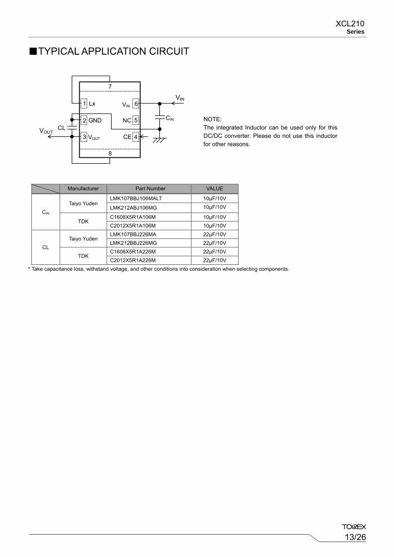
XCL210Series
TYPICAL APPLICATION CIRCUIT
Manufacturer Part Number VALUE
CIN Taiyo Yuden
LMK107BBJ106MALT 10μF/10V
LMK212ABJ106MG 10μF/10V
TDK C1608X5R1A106M 10μF/10V C2012X5R1A106M 10μF/10V
CL Taiyo Yuden
LMK107BBJ226MA 22μF/10V LMK212BBJ226MG 22μF/10V
TDK C1608X5R1A226M 22μF/10V C2012X5R1A226M 22μF/10V
* Take capacitance loss, withstand voltage, and other conditions into consideration when selecting components.
CIN
CL
7
8
1
2
3 4
5
6
GND
VINLx
CEVOUT
NC
VIN
VOUT
NOTE: The integrated Inductor can be used only for this DC/DC converter. Please do not use this inductor for other reasons.

14/26
XCL210 Series OPERATIONAL EXPLANATION The XCL210 series consists of a reference voltage supply, PFM comparator, Pch driver Tr, Nch synchronous rectification switch Tr, current sensing circuit, PFM control circuit, CE control circuit, and others. (Refer to the block diagram below.)
An ultra-low quiescent current circuit and synchronous rectification enable a significant reduction of dissipation in the IC, and the IC operates with high efficiency at both light loads and heavy loads. Current limit PFM is used for the control method, and even when switching current superposition occurs, increases of output voltage ripple are suppressed, allowing use over a wide voltage and current range. The IC is compatible with low-capacitance ceramic capacitors, and a small, high-performance step-down DC-DC converter can be created. The actual output voltage VOUT(E) in the electrical characteristics is the threshold voltage of the PFM comparator in the block diagram. Therefore the average output voltage of the step-down circuit, including peripheral components, depends on the ripple voltage. Before use, test fully using the actual device. <Reference voltage supply (VREF)> Reference voltage for stabilization of the output voltage of the IC. <PFM control> (1) The feedback voltage (FB voltage) is the voltage that results from dividing the output voltage with the IC internal dividing resistors RFB1 and RFB2. The PFM comparator compares this FB voltage to VREF. When the FB voltage is lower than VREF, the PFM comparator sends a signal to the buffer driver through the PFM control circuit to turn on the Pch driver Tr. When the FB voltage is higher than VREF, the PFM comparator sends a signal to prevent the Pch driver Tr from turning on. (2) When the Pch driver Tr is on, the current sense circuit monitors the current that flows through the Pch driver Tr connected to the Lx pin. When the current reaches the set PFM switching current (IPFM), the current sense circuit sends a signal to the buffer driver through the PFM control circuit. This signal turns off the Pch driver Tr and turns on the Nch synchronous rectification switch Tr. (3) The on time (off time) of the Nch synchronous rectification switch Tr is dynamically optimized inside the IC. After the off time elapses and the PFM comparator detects that the VOUT voltage is higher than the set voltage, the PFM comparator sends a signal to the PFM control circuit that prevents the Pch driver Tr from turning on. However, if the VOUT voltage is lower than the set voltage, the PFM comparator starts Pch driver Tr on.
VLX
VOUT
ILX
VLX
VOUT
ILX
VIN=VCE=3.6V、VOUT=1.8V、IOUT=5mA、L=8.0μH、CL=22uF、Ta=25 VIN=VCE=3.6V、VOUT=1.8V、IOUT=30mA、L=8.0μH、CL=22uF、Ta=25
VOUT(E) Voltage
VLX : 2[V/div]
VOUT : 50[mV/div]
ILX : 100[mA/div]
10[μs/div] 10[μs/div]
IPFM
<BLOCK DIAGRAM TYPE A/B/F > <BLOCK DIAGRAM TYPE C/D/H >
Lx
Inductor
GND
L2 L1
VIN
VOUT
CE
PFM Comparator
R2
R1
SynchBufferDrive
PFMController
Vref
ShortProtection
CFB
CurrentSense
UVLOVIN Start Up
Controller
CE Controller Logic
VDD
VDD
Lx
Inductor
GND
L2 L1
VIN
VOUT
CE
PFM Comparator
R2
R1
SynchBufferDrive
PFMController
Vref
ShortProtection
CFB
CurrentSenseCL
Discharge
UVLOVIN Start Up
Controller
CE Controller Logic
VDD
VDD

15/26
XCL210Series
OPERATIONAL EXPLANATION (Continued) By continuously adjusting the interval of the linked operation of (1), (2) and (3) above in response to the load current, the output voltage is stabilized with high efficiency from light loads to heavy loads. <PFM Switching Current > The PFM switching current monitors the current that flows through the Pch driver Tr, and is a value that limits the Pch driver Tr current. The Pch driver Tr remains on until the coil current reaches the PFM switching current (IPFM). An approximate value for this on-time tON can be calculated using the following equation: tON = L × IPFM / (VIN – VOUT) <Maximum on-time function> To avoid excessive ripple voltage in the event that the coil current does not reach the PFM switching current within a certain interval even though the Pch driver Tr has turned on and the FB voltage is above VREF, the Pch driver Tr can be turned off at any timing using the maximum on-time function of the PFM control circuit. If the Pch driver Tr turns off by the maximum on-time function instead of the current sense circuit, the Nch synchronous rectification switch Tr will not turn on and the coil current will flow to the VOUT pin by means of the parasite diode of the Nch synchronous rectification switch Tr.
<Through mode> When the VIN voltage is lower than the output voltage, through mode automatically activates and the Pch driver Tr stays on continuously. (1) In through mode, when the load current is increased and the current that flows through the Pch driver Tr reaches a load current that is several tens of mA lower than the set PFM switching current (IPFM), the current sense circuit sends a signal through the PFM control circuit to the buffer driver. This signal turns off the Pch driver Tr and turns on the Nch synchronous rectification switch Tr. (2) After the on-time (off-time) of the Nch synchronous rectification switch Tr, the Pch driver Tr turns on until the current reaches the set PFM switching current (IPFM) again. If the load current is large as described above, operations (1) and (2) above are repeated. If the load current is several tens of mA lower than the PFM switching current (IPFM), the Pch driver Tr stays on continuously.
<VIN start mode> When the VIN voltage rises, VIN start mode stops the short-circuit protection function during the interval until the FB voltage approaches VREF. After the VIN voltage rises and the FB voltage approaches VREF by step-down operation, VIN start mode is released. In order to prevent an excessive rush current while VIN start mode is activated, the coil current flows to the VOUT pin by means of the parasitic diode of the Nch synchronous rectification Tr. In VIN start mode as well, the coil current is limited by the PFM switching current.
<Short-circuit protection function> The short-circuit protection function monitors the VOUT voltage. In the event that the VOUT pin is accidentally shorted to GND or an excessive load current causes the VOUT voltage to drop below the set short-circuit protection voltage, the short-circuit protection function activates, and turns off and latches the Pch driver Tr at any selected timing. Once in the latched state, the IC is turned off and then restarted from the CE pin, or operation is started by re-applying the VIN voltage.
<UVLO function> When the VIN pin voltage drops below the UVLO detection voltage, the IC stops switching operation at any selected timing, turns off the Pch driver Tr and Nch synchronous rectification switch Tr (UVLO mode). When the VIN pin voltage recovers and rises above the UVLO release voltage, the IC restarts operation. <CL discharge function> On the XCL210 series, a CL discharge function is available as an option (Type C/D/H). This function enables quick discharging of the CL load capacitance when “L” voltage is input into the CE pin by the Nch Tr connected between the VOUT-GND pins, or in UVLO mode. This prevents malfunctioning of the application in the event that a charge remains on CL when the IC is stopped. The discharge time is determined by CL and the CL discharge resistance RDCHG, including the Nch Tr (refer to the diagram below). Using this time constant τ= CL×RDCHG, the discharge time of the output voltage is calculated by means of the equation below.
V = VOUT × e - t /τ, or in terms of t, t = τIn(VOUT / V) V: Output voltage after discharge
VOUT : Set output voltage t: Discharge time CL: Value of load capacitance (CL) RDCHG : Value of CL discharge resistance Varies by power supply voltage. τ: CL × RDCHG
The CL discharge function is not available on the Type A/B/F.

16/26
XCL210 Series NOTE ON USE 1. Be careful not to exceed the absolute maximum ratings for externally connected components and this IC. 2. The DC/DC converter characteristics greatly depend not only on the characteristics of this IC but also on those of externally connected
components, so refer to the specifications of each component and be careful when selecting the components. Be especially careful of the characteristics of the capacitor used for the load capacity CL and use a capacitor with B characteristics (JIS Standard) or an X7R/X5R (EIA Standard) ceramic capacitor.
3. Use a ground wire of sufficient strength. Ground potential fluctuation caused by the ground current during switching could cause the IC operation
to become unstable, so reinforce the area around the GND pin of the IC in particular. 4. Mount the externally connected components in the vicinity of the IC. Also use short, thick wires to reduce the wire impedance. 5. When the voltage difference between VIN and VOUT is small, switching energy increases and there is a possibility that the ripple voltage will be
too large. Before use, test fully using the actual device. 6. The CE pin does not have an internal pull-up or pull-down, etc. Apply the prescribed voltage to the CE pin. 7. If other than the recommended inductance and capacitance values are used, excessive ripple voltage or a drop in efficiency may result. 8. If other than the recommended inductance and capacitance values are used, a drop in output voltage when the load is excessive may cause
the short-circuit protection function to activate. Before use, test fully using the actual device. 9. At high temperature, excessive ripple voltage may occur and cause a drop in output voltage and efficiency. Before using at high temperature,
test fully using the actual device 10. At light loads or when IC operation is stopped, leakage current from the Pch driver Tr may cause the output voltage to rise. 11. The average output voltage may vary due to the effects of output voltage ripple caused by the load current. Before use, test fully using the
actual device. 12. If the CL capacitance or load current is large, the output voltage rise time will lengthen when the IC is started, and coil current overlay may
occur during the interval until the output voltage reaches the set voltage (refer to the diagram below).
13. When the IC is started, the short-circuit protection function does not operate during the interval until the VOUT voltage reaches a value near the
set voltage. 14. If the IC is started at a VIN voltage that activates through mode, it is possible that the short-circuit protection function will not operate. Before
use, test fully using the actual device. 15. If the load current is excessively large when the IC is started, it is possible that the VOUT voltage will not rise to the set voltage. Before use, test
fully using the actual device.
XCL210A Series、VIN=VCE=0→6.0V、VOUT=1.0V、IOUT=200mA、CL=22uF、Ta=25

17/26
XCL210Series
NOTE ON USE (Continued)
16. In actual operation, the maximum on-time depends on the peripheral components, input voltage, and load current. Before use, test fully using the actual device.
17. When the VIN voltage is turned on and off continuously, excessive rush current may occur while the voltage is on. Before use, test fully using
the actual device. 18. When the VIN voltage is high, the Pch driver may change from on to off before the coil current reaches the PFM switching current (IPFM), or
before the maximum on-time elapses. Before use, test fully using the actual device. 19. When the IC change to the Through Mode at light load, the supply current of this IC can increase in some cases. 20. For temporary, transitional voltage drop or voltage rising phenomenon, the IC is liable to malfunction should the ratings be exceeded. 21. Torex places an importance on improving our products and their reliability.
We request that users incorporate fail-safe designs and post-aging protection treatment when using Torex products in their systems. 22. The UVLO function can be activated when the UVLO hysteresis width gets to about 0mV and after several tens ms elapses at light loads.
Before use, test fully using the actual device. 23. Please use within the power dissipation range below. Please also note that the power dissipation may changed by test conditions, the
power dissipation figure shown is PCB mounted.
the power loss of micro DC/DC according to the following formula:
power loss = VOUT×IOUT×((100/EFFI) – 1) (W) VOUT : Output Voltage (V) IOUT : Output Current (A) EFFI : Conversion Efficiency (%) Measurement Condition (Reference data) Condition: Mount on a board Ambient: Natural convection Soldering: Lead (Pb) free Board: Dimensions 40 x 40 mm (1600 mm2 in one side)
Copper (Cu) traces occupy 50% of the board area In top and back faces Package heat-sink is tied to the copper traces
Material: Glass Epoxy (FR-4) Thickness: 1.6mm Through-hole: 4 x 0.8 Diameter
Evaluation Board (unit: mm)
Pd vs Operating Temperature Pakage Body Temperature vs Operating Temperature

18/26
XCL210 Series NOTE ON USE (Continued) Instructions of pattern layouts 1. To suppress fluctuations in the VIN potential, connect a bypass capacitor (CIN) in the shortest path between the VIN pin and ground pin. 2. Please mount each external component as close to the IC as possible. 3. Wire external components as close to the IC as possible and use thick, short connecting traces to reduce the circuit impedance. 4. Make sure that the ground traces are as thick as possible, as variations in ground potential caused by high ground currents at the time of
switching may result in instability of the IC. 5. Internal driver transistors bring on heat because of the transistor current and ON resistance of the driver transistors.
Recommended Pattern Layout
Top view Back side top view

19/26
XCL210Series
TYPICAL PERFORMANCE CHARACTERISTICS 1) Output Voltage vs. Output Current
3.0
3.1
3.2
3.3
3.4
3.5
3.6
0.01 0.1 1 10 100
Out
put V
olta
ge: V
OU
T[V
]
Output Current: IOUT [mA]
Vin=4.2V,CL=22uFVin=4.2V,CL=22uF×2Vin=5.0V,CL=22uFVin=5.0V,CL=22uF×2
1.5
1.6
1.7
1.8
1.9
2.0
2.1
0.01 0.1 1 10 100
Out
put V
olta
ge: V
OU
T[V
]
Output Current: IOUT [mA]
Vin=3.0V,CL=22uFVin=3.0V,CL=22uF×2Vin=4.2V,CL=22uFVin=4.2V,CL=22uF×2
0.9
1.0
1.1
1.2
1.3
1.4
1.5
0.01 0.1 1 10 100
Out
put V
olta
ge: V
OU
T[V
]
Output Current: IOUT [mA]
Vin=3.0V,CL=22uFVin=3.0V,CL=22uF×2Vin=4.2V,CL=22uFVin=4.2V,CL=22uF×2
XCL210B121GR-G/XCL210D121GR-G
XCL210B181GR-G/XCL210D181GR-G
XCL210A121GR-G/XCL210C121GR-G
XCL210A181GR-G/XCL210C181GR-G
XCL210A331GR-G/XCL210C331GR-G XCL210B331GR-G/XCL210D331GR-G

20/26
XCL210 Series TYPICAL PERFORMANCE CHARACTERISTICS (Continued) 2) Efficiency vs. Output Current
0
20
40
60
80
100
0.01 0.1 1 10 100
Effi
cien
cy: E
FFI [
%]
Output Current: IOUT [mA]
Vin=3.0V,CL=22uFVin=3.0V,CL=22uF×2Vin=4.2V,CL=22uFVin=4.2V,CL=22uF×2
0
20
40
60
80
100
0.01 0.1 1 10 100
Effi
cien
cy: E
FFI [
%]
Output Current: IOUT [mA]
Vin=4.2V,CL=22uFVin=4.2V,CL=22uF×2Vin=5.0V,CL=22uFVin=5.0V,CL=22uF×2
0
20
40
60
80
100
0.01 0.1 1 10 100
Effi
cien
cy: E
FFI [
%]
Output Current: IOUT [mA]
Vin=3.0V,CL=22uFVin=3.0V,CL=22uF×2Vin=4.2V,CL=22uFVin=4.2V,CL=22uF×2
0
20
40
60
80
100
0.01 0.1 1 10 100
Effi
cien
cy: E
FFI [
%]
Output Current: IOUT [mA]
Vin=3.0V,CL=22uFVin=3.0V,CL=22uF×2Vin=4.2V,CL=22uFVin=4.2V,CL=22uF×2
XCL210B121GR-G/XCL210D121GR-G
XCL210B181GR-G/XCL210D181GR-G
XCL210A121GR-G/XCL210C121GR-G
XCL210A181GR-G/XCL210C181GR-G
XCL210A331GR-G/XCL210C331GR-G XCL210B331GR-G/XCL210D331GR-G

21/26
XCL210Series
TYPICAL PERFORMANCE CHARACTERISTICS (Continued) 3) Ripple Voltage vs. Output Current
XCL210B121GR-G/XCL210D121GR-G
XCL210B181GR-G/XCL210D181GR-G
XCL210A121GR-G/XCL210C121GR-G
XCL210A181GR-G/XCL210C181GR-G
XCL210A331GR-G/XCL210C331GR-G XCL210B331GR-G/XCL210D331GR-G
0
50
100
150
200
0.01 0.1 1 10 100
Rip
ple
Vol
tage
:Vr [
mV
]
Output Current: IOUT [mA]
Vin=4.2V,CL=22uFVin=4.2V,CL=22uF×2Vin=5.0V,CL=22uFVin=5.0V,CL=22uF×2
0
50
100
150
200
0.01 0.1 1 10 100
Rip
ple
Vol
tage
: Vr [
mV
]
Output Current: IOUT [mA]
Vin=4.2V,CL=22uFVin=4.2V,CL=22uF×2Vin=5.0V,CL=22uFVin=5.0V,CL=22uF×2
0
50
100
150
200
0.01 0.1 1 10 100
Rip
ple
Vol
tage
: Vr [
mV]
Output Current: IOUT [mA]
Vin=3.0V,CL=22uFVin=3.0V,CL=22uF×2Vin=4.2V,CL=22uFVin=4.2V,CL=22uF×2
0
50
100
150
200
0.01 0.1 1 10 100
Rip
ple
Vol
tage
: Vr[
mV
]
Output Current: IOUT [mA]
Vin=3.0V,CL=22uFVin=3.0V,CL=22uF×2Vin=4.2V,CL=22uFVin=4.2V,CL=22uF×2
0
50
100
150
200
0.01 0.1 1 10 100
Rip
ple
Vol
tage
: Vr [
mV]
Output Current: IOUT [mA]
Vin=3.0V,CL=22uFVin=3.0V,CL=22uF×2Vin=4.2V,CL=22uFVin=4.2V,CL=22uF×2
0
50
100
150
200
0.01 0.1 1 10 100
Rip
ple
Vol
tage
: Vr [
mV]
Output Current: IOUT [mA]
Vin=3.0V,CL=22uFVin=3.0V,CL=22uF×2Vin=4.2V,CL=22uFVin=4.2V,CL=22uF×2

22/26
XCL210 Series TYPICAL PERFORMANCE CHARACTERISTICS (Continued) 4) Ambient Temperature vs. Output Voltage
1.0
1.1
1.2
1.3
1.4
-40 -20 0 20 40 60 80 100
Out
put V
olta
ge: V
OU
T[V
]
Ambient Temperature : Ta []
IOUT=0.1mAIOUT=1mAIOUT=10mAIOUT=100mA
VIN=3.6V
1.0
1.1
1.2
1.3
1.4
-40 -20 0 20 40 60 80 100
Out
put V
olta
ge: V
OU
T[V
]
Ambient Temperature : Ta []
IOUT=0.1mAIOUT=1mAIOUT=10mA
VIN=3.6V
1.6
1.7
1.8
1.9
2.0
-40 -20 0 20 40 60 80 100
Out
put V
olta
ge: V
OU
T[V
]
Ambient Temperature : Ta []
IOUT=0.1mAIOUT=1mAIOUT=10mA
VIN=3.6
1.6
1.7
1.8
1.9
2.0
-40 -20 0 20 40 60 80 100
Out
put V
olta
ge: V
OU
T[V
]
Ambient Temperature : Ta []
IOUT=0.1mAIOUT=1mAIOUT=10mAIOUT=100mA
VIN=3.6V
3.1
3.2
3.3
3.4
3.5
-40 -20 0 20 40 60 80 100
Out
put V
olta
ge: V
OU
T[V
]
Ambient Temperature : Ta []
IOUT=0.1mAIOUT=1mAIOUT=10mAIOUT=100mA
VIN=5.0V
3.1
3.2
3.3
3.4
3.5
-40 -20 0 20 40 60 80 100
Out
put V
olta
ge: V
OU
T[V
]
Ambient Temperature : Ta []
IOUT=0.1mAIOUT=1mAIOUT=10mA
VIN=5.0V
XCL210B121GR-G/XCL210D121GR-G XCL210A121GR-G/XCL210C121GR-G
XCL210A181GR-G/XCL210C181GR-G
XCL210A331GR-G/XCL210C331GR-G
XCL210B181GR-G/XCL210D181GR-G
XCL210B331GR-G/XCL210D331GR-G
23/26
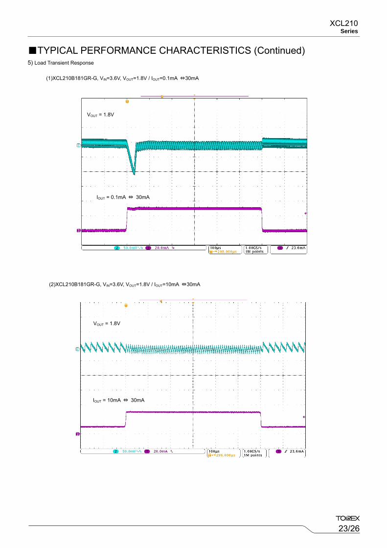
XCL210Series
TYPICAL PERFORMANCE CHARACTERISTICS (Continued) 5) Load Transient Response
(1)XCL210B181GR-G, VIN=3.6V, VOUT=1.8V / IOUT=0.1mA ⇔30mA
(2)XCL210B181GR-G, VIN=3.6V, VOUT=1.8V / IOUT=10mA ⇔30mA
IOUT = 0.1mA ⇔ 30mA
VOUT = 1.8V
IOUT = 10mA ⇔ 30mA
VOUT = 1.8V

24/26
XCL210 Series PACKAGING INFORMATION
CL-2025-02 (unit: mm)
Reference Pattern Layout (unit: mm) Reference Metal Mask Design (unit: mm)
* Implementation of CL-2025-02 is recommended within accuracy 0.05mm.
External Lead
25/26
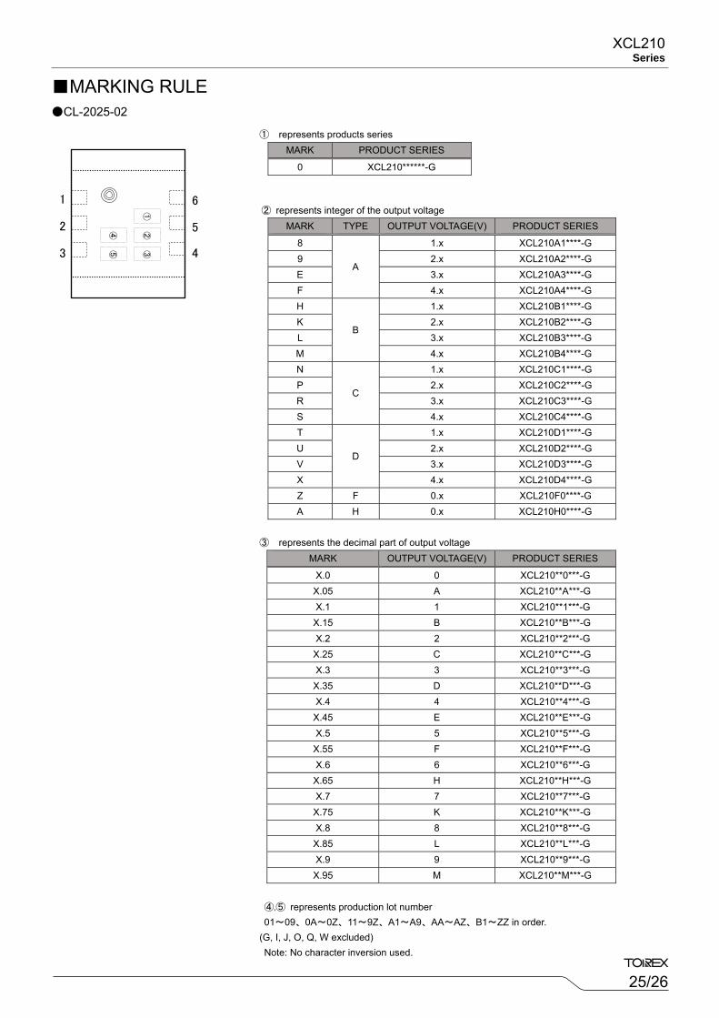
XCL210Series
MARKING RULE CL-2025-02
① represents products series
② represents integer of the output voltage
③ represents the decimal part of output voltage
④,⑤ represents production lot number 01~09、0A~0Z、11~9Z、A1~A9、AA~AZ、B1~ZZ in order.
(G, I, J, O, Q, W excluded) Note: No character inversion used.
MARK PRODUCT SERIES
0 XCL210******-G
MARK TYPE OUTPUT VOLTAGE(V) PRODUCT SERIES
8
A
1.x XCL210A1****-G 9 2.x XCL210A2****-G E 3.x XCL210A3****-G F 4.x XCL210A4****-G H
B
1.x XCL210B1****-G K 2.x XCL210B2****-G L 3.x XCL210B3****-G M 4.x XCL210B4****-G N
C
1.x XCL210C1****-G P 2.x XCL210C2****-G R 3.x XCL210C3****-G S 4.x XCL210C4****-G T
D
1.x XCL210D1****-G U 2.x XCL210D2****-G V 3.x XCL210D3****-G X 4.x XCL210D4****-G Z F 0.x XCL210F0****-G A H 0.x XCL210H0****-G
MARK OUTPUT VOLTAGE(V) PRODUCT SERIES
X.0 0 XCL210**0***-G X.05 A XCL210**A***-G X.1 1 XCL210**1***-G
X.15 B XCL210**B***-G X.2 2 XCL210**2***-G
X.25 C XCL210**C***-G X.3 3 XCL210**3***-G
X.35 D XCL210**D***-G X.4 4 XCL210**4***-G
X.45 E XCL210**E***-G X.5 5 XCL210**5***-G
X.55 F XCL210**F***-G X.6 6 XCL210**6***-G
X.65 H XCL210**H***-G X.7 7 XCL210**7***-G
X.75 K XCL210**K***-G X.8 8 XCL210**8***-G
X.85 L XCL210**L***-G X.9 9 XCL210**9***-G
X.95 M XCL210**M***-G
⑤④
①②
1
2
3
6
5
4
③

26/26
XCL210 Series
1. The product and product specifications contained herein are subject to change without notice to improve performance characteristics. Consult us, or our representatives before use, to confirm that the information in this datasheet is up to date.
2. The information in this datasheet is intended to illustrate the operation and characteristics of our
products. We neither make warranties or representations with respect to the accuracy or completeness of the information contained in this datasheet nor grant any license to any intellectual property rights of ours or any third party concerning with the information in this datasheet.
3. Applicable export control laws and regulations should be complied and the procedures required by
such laws and regulations should also be followed, when the product or any information contained in this datasheet is exported.
4. The product is neither intended nor warranted for use in equipment of systems which require extremely
high levels of quality and/or reliability and/or a malfunction or failure which may cause loss of human life, bodily injury, serious property damage including but not limited to devices or equipment used in 1) nuclear facilities, 2) aerospace industry, 3) medical facilities, 4) automobile industry and other transportation industry and 5) safety devices and safety equipment to control combustions and explosions. Do not use the product for the above use unless agreed by us in writing in advance.
5. Although we make continuous efforts to improve the quality and reliability of our products; nevertheless
Semiconductors are likely to fail with a certain probability. So in order to prevent personal injury and/or property damage resulting from such failure, customers are required to incorporate adequate safety measures in their designs, such as system fail safes, redundancy and fire prevention features.
6. Our products are not designed to be Radiation-resistant.
7. Please use the product listed in this datasheet within the specified ranges.
8. We assume no responsibility for damage or loss due to abnormal use.
9. All rights reserved. No part of this datasheet may be copied or reproduced unless agreed by Torex
Semiconductor Ltd in writing in advance.
TOREX SEMICONDUCTOR LTD.