Embed Size (px)
Citation preview

1/22
XCL201/XCL202 Series Inductor Built-in Step-Down “micro DC/DC” Converters
0
20
40
60
80
100
0.01 0.1 1 10 100 1000
Output Current:IOUT (mA)
Effic
ency
:EFF
I(%)
5.0V
VOUT=3.3V
XCL202(PWM/PFM)
XCL201(PWM)
4.2V
VIN= 5.5V
TYPICAL PERFORMANCE CHARACTERISTICS
APPLICATIONS Mobile phones, Smart phones
Bluetooth Headsets
WiMAX PDAs, MIDs, UMPCs
Portable game consoles
Digital cameras, Camcorders
SSD(Solid State Drive)
PND(Portable Navigation Device)
TYPICAL APPLICATION CIRCUIT
ETR2802-006
XCL201B331BR/XCL202B331BR
VIN
Vss
CE
LX
Vss
VOUT
CL 10μF
4.7μF CIN
L1
L2
400mA
XCL201/XCL202 Series
GENERAL DESCRIPTION The XCL201/XCL201 series is a synchronous step-down micro DC/DC converter which integrates an inductor and a control IC in one tiny package (2.5mm×2.0mm, h=1.0mm). A stable power supply with an output current of 400mA is configured using only two capacitors connected externally. Operating voltage range is from 2.0V to 6.0V. Output voltage is internally set in a range from 0.8V to 4.0V in increments of 0.05V. The device is operated by 1.2MHz, and includes 0.42ΩP-channel driver transistor and 0.52ΩN-channel switching transistor. As for operation mode, the XCL201 series is PWM control, the XCL202 series is automatic PWM/PFM switching control, allowing fast response, low ripple and high efficiency over the full range of loads (from light load to heavy load). During stand-by, the device is shutdown to reduce current consumption to as low as 1.0μA or less. With the built-in UVLO (Under Voltage Lock Out) function, the internal driver transistor is forced OFF when input voltage becomes 1.4V or lower. The series provide short-time turn-on by the soft start function internally set in 0.25ms (TYP). The series integrate CL auto discharge function which enables the electric charge stored at the output capacitor CL to be discharged via the internal auto-discharge switch located between the LX and VSS pins. When the devices enter stand-by mode, output voltage quickly returns to the VSS level as a result of this function.
FEATURESUltra Small : 2.5mm×2.0mm, h=1.0mm Input Voltage : 2.0V ~ 6.0V Output Voltage : 0.8V ~ 4.0V (±2.0%) High Efficiency : 92%(VIN=4.2V,VOUT=3.3V) Output Current : 400mA Oscillation Frequency : 1.2MHz (±15%) Maximum Duty Cycle : 100% Output Capacitor : Low ESR Ceramic Function : Current Limiter Circuit (Constant Current & Latching) Soft-Start Circuit Built-In CL Discharge Control Methods : PWM (XCL201) PWM/PFM Auto (XCL202) Operating Ambient Temperature : -40~+85 Environmentally Friendly : EU RoHS Compliant, Pb Free
(TOP VIEW)
* “L1 and LX”, and “L2 and VOUT” is connected by wiring.
GreenOperation Compatible
2/22
XCL201/XCL202 Series
PIN CONFIGURATION
PIN ASSIGNMENT
PRODUCT CLASSIFICATION Ordering Information XCL201①②③④⑤⑥-⑦(*1) Fixed PWM control
XCL202①②③④⑤⑥-⑦(*1) PWM / PFM automatic switching control
PIN NUMBER PIN NAME FUNCTIONS
1 Lx Switching Output 2,5 VSS Ground 3 VOUT Output Voltage 4 CE Chip Enable 6 VIN Power Input 7 L1
Inductor Electrodes 8 L2
DESIGNATOR ITEM SYMBOL DESCRIPTION
① Functions selection B CL auto discharge, High speed soft-start
②③ Output Voltage 08~40
Output voltage options e.g. 1.2V → ②=1, ③=2 1.25V → ②=1, ③=C 0.05V increments : 0.05=A, 0.15=B, 0.25=C, 0.35=D, 0.45=E, 0.55=F, 0.65=H, 0.75=K, 0.85=L, 0.95=M
④ Oscillation Frequency 1 1.2MHz
⑤⑥-⑦ Package
(Order Unit) BR-G(*2) CL-2025 (3,000pcs/Reel)
ER-G(*3) CL-2025-02 (3,000pcs/Reel)
(BOTTOM VIEW)
L1
L2
7
8
V IN 6
Vss 5
4
1 Lx
2 Vss
3 VOUT CE
* It should be connected the VSS pin (No. 2 and 5) to the GND pin. * If the dissipation pad needs to be connected to other pins, it should be connected to the GND pin.* Please refer to pattern layout page for the connecting to PCB.
(*1) The “-G” suffix denotes Halogen and Antimony free as well as being fully EU RoHS compliant. (*2) BR-G is storage temperature range "-40 ~ + 105 ". (*3) ER-G is storage temperature range "-40 ~ + 125 ".

3/22
XCL201/XCL202Series
BLOCK DIAGRAM
ABSOLUTE MAXIMUM RATINGS Ta = 25
CE/
CE
R2
R1ErrorAmp.
Vref withSoft Start,
CE
PhaseCompensation
Current FeedbackCurrent Limit
PWMComparator
LogicSynchBufferDrive
R3
R4
UVLO
UVLO Cmp Ramp WaveGenerator
OSC
Lx
VSS
VIN
VOUT
CEControlLogic
VSHORT
FB
CFB
Inductor
VSS
L2 L1
PWM/PFMSelector
PARAMETER SYMBOL RATINGS UNITS VIN Pin Voltage VIN - 0.3 ~ +6.5 V LX Pin Voltage VLX - 0.3 ~ VIN + 0.3 ≦ +6.5 V
VOUT Pin Voltage VOUT - 0.3 ~ +6.5 V CE Pin Voltage VCE - 0.3 ~ +6.5 V LX Pin Current ILX ±1500 mA
Power Dissipation Pd 1000(*1) mW Operating Ambient Temperature Topr - 40~ +85
Storage Temperature(*2) CL-2025
Tstg - 40 ~ +105
CL-2025-02 - 40 ~ +125
XCL201B / XCL202B Series
NOTE: The XCL201 offers a fixed PWM control, a signal from CE Control Logic to PWM/PFM Selector is fixed to "L" level inside. The XCL202 control scheme is PWM/PFM automatic switching, a signal from CE Control Logic to PWM/PFM Selector is fixed to "H" level inside. The diodes placed inside are ESD protection diodes and parasitic diodes.
(*1) The power dissipation figure shown is PCB mounted (40mm×40mm, t=1.6mm, Glass Epoxy FR-4). Please refer to page 12 for details.
(*2) Storage temperature, are divided by the product specification of the package.

4/22
XCL201/XCL202 Series
ELECTRICAL CHARACTERISTICS
XCL201B121BR/XCL202B121BR/XCL201B121ER/XCL202B121ER, VOUT=1.2V, fOSC=1.2MHz, Ta=25
PARAMETER SYMBOL CONDITIONS MIN. TYP. MAX. UNITS CIRCUIT
Output Voltage VOUT When connected to external components, VIN=VCE=5.0V, IOUT=30mA 1.176 1.200 1.224 V ①
Operating Voltage Range VIN 2.0 - 6.0 V ①
Maximum Output Current IOUTMAX VIN=VOUT(T)+2.0V, VCE=1.0V When connected to external components (*8) 400 - - mA ①
UVLO Voltage VUVLO VCE=VIN,VOUT=0VVoltage which Lx pin holding “L” level (*1, *10) 1.00 1.40 1.78 V ②
Supply Current (XCL201) IDD VIN=VCE=5.0V, VOUT=VOUT(T)×1.1V
- 22 50 μA ②
Supply Current (XCL202) - 15 33 Stand-by Current ISTB VIN=5.0V, VCE=0V, VOUT= VOUT(T)×1.1V - 0 1.0 μA ③
Oscillation Frequency fOSC When connected to external components, VIN=VOUT(T)+2.0V, VCE=1.0V , IOUT=100mA 1020 1200 1380 kHz ①
PFM Switching Current (*11) IPFM When connected to external components, VIN=VOUT(T)+2.0V, VCE=VIN , IOUT=1mA 140 180 240 mA ⑩
PFM Duty Limit (*11) DTYLIMIT_PFM VCE=VIN = 2.0V, IOUT=1mA - 200 300 % ①
Maximum Duty Cycle MAXDTY VIN=VCE=5.0V, VOUT=VOUT (T)×0.9V 100 - - % ③
Minimum Duty Cycle MINDTY VIN=VCE=5.0V, VOUT=VOUT (T)×1.1V - - 0 % ③
Efficiency (*2) EFFI When connected to external components, VCE=VIN=VOUT (T)+1.2V, IOUT=100mA - 86 - % ①
Lx SW "H" ON Resistance 1 RLxH1 VIN=VCE=5.0V, VOUT=0V,ILX=100mA (*3) - 0.35 0.55 Ω ④
Lx SW "H" ON Resistance 2 RLxH2 VIN=VCE=3.6V, VOUT=0V,ILX=100mA (*3) - 0.42 0.67 Ω ④
Lx SW "L" ON Resistance 1 RLxL1 VIN=VCE=5.0V (*4) - 0.45 0.65 Ω - Lx SW "L" ON Resistance 2 RLxL2 VIN=VCE=3.6V (*4) - 0.52 0.77 Ω -
Lx SW "H" Leakage Current (*5) ILeakH VIN=VOUT=5.0V, VCE=0V, LX=0V - 0.01 1.0 μA ⑨
Current Limit (*9) ILIM VIN=VCE=5.0V, VOUT=VOUT (T)×0.9V (*7) 700 800 1000 mA ⑥
Output Voltage Temperature Characteristics
VOUT/ (VOUT・Topr)
IOUT=30mA -40≦Topr≦85 - ±100 - ppm/ ①
CE "H" Voltage VCEH VOUT=0V, Applied voltage to VCE, Voltage changes Lx to “H” level (*10) 0.65 - 6.0 V ③
CE "L" Voltage VCEL VOUT=0V, Applied voltage to VCE, Voltage changes Lx to “L” level (*10) VSS - 0.25 V ③
CE "H" Current ICEH VIN=VCE=5.0V, VOUT=0V - 0.1 - 0.1 μA ⑤
CE "L" Current ICEL VIN=5.0V, VCE=0V, VOUT=0V - 0.1 - 0.1 μA ⑤
Soft Start Time tSS When connected to external components, VCE=0V→VIN , IOUT=1mA - 0.25 0.40 ms ①
Latch Time tLAT VIN=VCE=5.0V, VOUT=0.8×VOUT(T)
Short Lx at 1Ω resistance (*6) 1.0 - 20 ms ⑦
Short Protection Threshold Voltage VSHORT
Sweeping VOUT, VIN=VCE=5.0V, Short Lx at 1Ω resistance, VOUT voltage which Lx becomes “L” level within 1ms
0.450 0.600 0.750 V ⑦
CL Discharge RDCHG VIN=5.0V, LX=5.0V, VCE=0V, VOUT=open 200 300 450 Ω ⑧
Inductance Value L Test frequency=1MHz - 4.7 - μH - Allowed Inductor Current IDC ΔT=40 - 600 - mA -
Test conditions: Unless otherwise stated, VIN=5.0V, VOUT(T)=Nominal Voltage NOTE: (*1) Including hysteresis operating voltage range. (*2) EFFI= ( output voltage×output current ) / ( input voltage×input current) ×100 (*3) ON resistance (Ω)=(VIN - Lx pin measurement voltage) / 100mA (*4) Design value (*5) When temperature is high, a current of approximately 10μA (maximum) may leak. (*6) Time until it short-circuits VOUT with GND via 1Ω of resistor from an operational state and is set to Lx=0V from current limit pulse generating. (*7) When VIN is less than 2.4V, limit current may not be reached because voltage falls caused by ON resistance. (*8) When the difference between the input and the output is small, some cycles may be skipped completely before current maximizes. If current is further pulled from this state, output voltage will decrease because of P-ch driver ON resistance. (*9) Current limit denotes the level of detection at peak of coil current. (*10) “H”=VIN~VIN-1.2V, “L”=+0.1V~-0.1V (*11) IPFM and DTYLIMIT_PFM are defined only for the XCL202 series which have PFM control function. (Not for the XCL201 series)
5/22
XCL201/XCL202Series
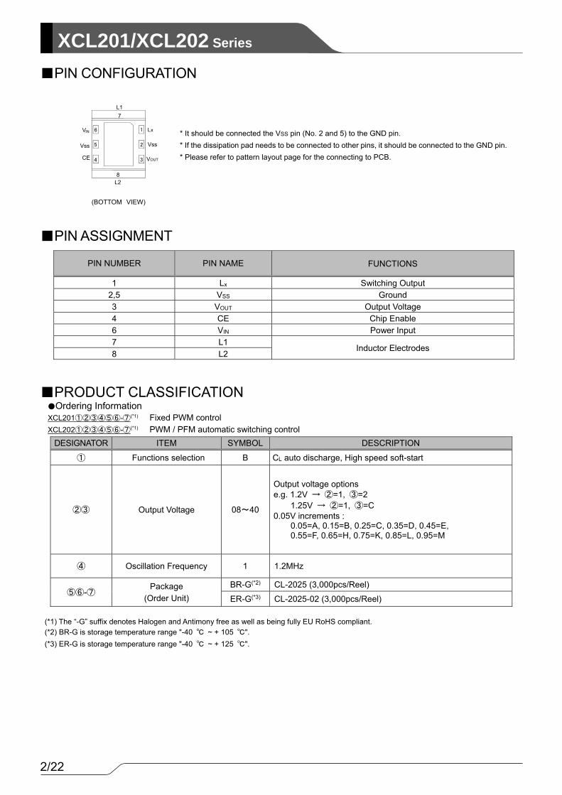
ELECTRICAL CHARACTERISTICS (Continued)
XCL201B181BR/XCL202B181BR/XCL201B181ER/XCL202B181ER ,VOUT=1.8V, fOSC=1.2MHz, Ta=25
PARAMETER SYMBOL CONDITIONS MIN. TYP. MAX. UNITS CIRCUIT
Output Voltage VOUT When connected to external components, VIN=VCE=5.0V, IOUT=30mA 1.764 1.800 1.836 V ①
Operating Voltage Range VIN 2.0 - 6.0 V ①
Maximum Output Current IOUTMAX VIN=VOUT(E)+2.0V, VCE=1.0V When connected to external components (*8) 400 - - mA ①
UVLO Voltage VUVLO VCE=VIN,VOUT=0V Voltage which Lx pin holding “L” level (*1, *10) 1.00 1.40 1.78 V ②
Supply Current (XCL201) IDD VIN=VCE=5.0V, VOUT=VOUT(T)×1.1V
- 22 50 μA ②
Supply Current (XCL202) - 15 33 Stand-by Current ISTB VIN=5.0V, VCE=0V, VOUT=VOUT(T)×1.1V - 0 1.0 μA ③
Oscillation Frequency fOSC When connected to external components, VIN=VOUT(T)+2.0V, VCE=1.0V , IOUT=100mA 1020 1200 1380 kHz ①
PFM Switching Current (*11) IPFM When connected to external components, VIN=VOUT(T)+2.0V, VCE=VIN , IOUT=1mA 120 160 200 mA ⑩
PFM Duty Limit (*11) DTYLIMIT_PFM VCE=VIN=VOUT(T) +0.5V, IOUT=1mA - 200 300 % ①
Maximum Duty Cycle MAXDTY VIN=VCE=5.0V, VOUT=VOUT (T)×0.9V 100 - - % ③
Minimum Duty Cycle MINDTY VIN=VCE=5.0V, VOUT=VOUT (T)×1.1V - - 0 % ③
Efficiency (*2) EFFI When connected to external components, VCE=VIN=VOUT (T)+1.2V, IOUT=100mA - 89 - % ①
Lx SW "H" ON Resistance 1 RLxH1 VIN=VCE=5.0V, VOUT=0V, ILX=100mA (*3) - 0.35 0.55 Ω ④
Lx SW "H" ON Resistance 2 RLxH2 VIN=VCE=3.6V, VOUT=0V, ILX=100mA (*3) - 0.42 0.67 Ω ④
Lx SW "L" ON Resistance 1 RLxL1 VIN=VCE=5.0V (*4) - 0.45 0.65 Ω - Lx SW "L" ON Resistance 2 RLxL2 VIN=VCE=3.6V (*4) - 0.52 0.77 Ω -
Lx SW "H" Leakage Current (*5) ILeakH VIN=VOUT=5.0V, VCE=0V, LX=0V - 0.01 1.0 μA ⑨
Current Limit (*9) ILIM VIN=VCE= 5.0V, VOUT=VOUT (T)×0.9V (*7) 700 800 1000 mA ⑥
Output Voltage Temperature Characteristics
VOUT/ (VOUT・Topr)
IOUT=30mA -40≦Topr≦85 - ±100 - ppm/ ①
CE "H" Voltage VCEH VOUT=0V, Applied voltage to VCE, Voltage changes Lx to “H” level (*10) 0.65 - 6.0 V ③
CE "L" Voltage VCEL VOUT=0V, Applied voltage to VCE, Voltage changes Lx to “L” level (*10) VSS - 0.25 V ③
CE "H" Current ICEH VIN=VCE=5.0V, VOUT=0V - 0.1 - 0.1 μA ⑤
CE "L" Current ICEL VIN=5.0V, VCE=0V, VOUT=0V - 0.1 - 0.1 μA ⑤
Soft Start Time tSS When connected to external components, VCE=0V→VIN , IOUT=1mA - 0.32 0.50 ms ①
Latch Time tLAT VIN=VCE=5.0V, VOUT=0.8×VOUT(T)
Short Lx at 1Ω resistance (*6) 1.0 - 20 ms ⑦
Short Protection Threshold Voltage VSHORT
Sweeping VOUT, VIN=VCE=5.0V, Short Lx at 1Ω resistance, VOUT voltage which Lx becomes “L” level within 1ms
0.675 0.900 1.125 V ⑦
CL Discharge RDCHG VIN=5.0V LX=5.0V VCE=0V VOUT=open 200 300 450 Ω ⑧
Inductance Value L Test frequency=1MHz - 4.7 - μH - Allowed Inductor Current IDC ΔT=40 - 600 - mA -
Test conditions: Unless otherwise stated, VIN=5.0V, VOUT (T)=Nominal VoltageNOTE: (*1) Including hysteresis operating voltage range. (*2) EFFI= ( output voltage×output current ) / ( input voltage×input current) ×100 (*3) ON resistance (Ω)=(VIN - Lx pin measurement voltage) / 100mA (*4) Design value (*5) When temperature is high, a current of approximately 10μA (maximum) may leak. (*6) Time until it short-circuits VOUT with GND via 1Ω of resistor from an operational state and is set to Lx=0V from current limit pulse generating. (*7) When VIN is less than 2.4V, limit current may not be reached because voltage falls caused by ON resistance. (*8) When the difference between the input and the output is small, some cycles may be skipped completely before current maximizes. If current is further pulled from this state, output voltage will decrease because of P-ch driver ON resistance. (*9) Current limit denotes the level of detection at peak of coil current. (*10) “H”=VIN~VIN-1.2V, “L”=+0.1V~-0.1V (*11) IPFM and DTYLIMIT_PFM are defined only for the XCL202 series which have PFM control function. (Not for the XCL201 series)

6/22
XCL201/XCL202 Series
ELECTRICAL CHARACTERISTICS (Continued)
The value and conditions are depends on setting output voltage. PFM Switching Current (IPFM) (XCL202)
NOMINAL OUTPUT VOLTAGE MIN. TYP. MAX.
0.8V≦VOUT(T) ≦1.2V 140mA 180mA 240mA 1.2V<VOUT(T)<1.8V 130mA 170mA 220mA 1.8V≦VOUT(T)≦4.0V 120mA 160mA 200mA
PFM Duty Limit DTYLIMIT_PFM (XCL202)
SETTING VOLTAGE CONDITIONS
0.8V≦VOUT(T)<1.0V VCE=VIN=2.0V, IOUT=1mA 1.0V≦VOUT(T)≦4.0V VCE=VIN=VOUT(T)+0.5V, IOUT=1mA
Soft-Start Time tSS
SERIES OUTPUT VOLTAGE MIN. TYP. MAX.
XCL201B
0.8V≦VOUT(T)<1.5V - 0.25ms 0.40ms
1.5V≦VOUT(T)<1.8V - 0.32ms 0.50ms
1.8V≦VOUT(T)<2.5V - 0.28ms 0.40ms
2.5V≦VOUT(T)≦4.0V - 0.32ms 0.50ms
XCL202B 0.8V≦VOUT(T)<2.5V - 0.28ms 0.40ms
2.5V≦VOUT(T)≦4.0V - 0.32ms 0.50ms
TYPICAL APPLICATION CIRCUIT XCL201/XCL202 Series
External Components CIN : 10V/4.7μF(Ceramic) CL : 6.3V/10μF(Ceramic)
NOTE: The Inductor can be used only for this DC/DC converter. Please do not use this inductor for the other reasons. Please use B, X5R, and X7R grades in temperature characteristics for CIN and CL capacitors. These grade ceramic capacitors minimize capacitance-loss as a function of voltage stress.
VIN
Vss Vss
Lx
VOUT CE
L1
L2
CIN
CL

7/22
XCL201/XCL202Series
OPERATIONAL DESCRIPTION
The XCL201/XCL202 series consists of a reference voltage source, ramp wave circuit, error amplifier, PWM comparator, phase compensation circuit, output voltage adjustment resistors, P-channel MOSFET driver transistor, N-channel MOSFET switching transistor for the synchronous switch, current limiter circuit, UVLO circuit with control IC, and an inductor. (See the block diagram below.) Using the error amplifier, the voltage of the internal voltage reference source is compared with the feedback voltage from the VOUT pin through split resistors, R1 and R2. Phase compensation is performed on the resulting error amplifier output, to input a signal to the PWM comparator to determine the turn-on time during PWM operation. The PWM comparator compares, in terms of voltage level, the signal from the error amplifier with the ramp wave from the ramp wave circuit, and delivers the resulting output to the buffer driver circuit to cause the Lx pin to output a switching duty cycle. This process is continuously performed to ensure stable output voltage. The current feedback circuit monitors the P-channel MOS driver transistor current for each switching operation, and modulates the error amplifier output signal to provide multiple feedback signals. This enables a stable feedback loop even when a low ESR capacitor such as a ceramic capacitor is used ensuring stable output voltage. <Reference Voltage Source> The reference voltage source provides the reference voltage to ensure stable output voltage of the DC/DC converter. <Ramp Wave Circuit> The ramp wave circuit determines switching frequency. The frequency is fixed internally 1.2MHz. Clock pulses generated in this circuit are used to produce ramp waveforms needed for PWM operation, and to synchronize all the internal circuits. <Error Amplifier> The error amplifier is designed to monitor output voltage. The amplifier compares the reference voltage with the feedback voltage divided by the internal split resistors, R1 and R2. When a feed back voltage is lower than the reference voltage, the output voltage of the error amplifier is increased. The gain and frequency characteristics of the error amplifier output are fixed internally to deliver an optimized signal to the mixer.
CE/
CE
R2
R1ErrorAmp.
Vref withSoft Start,
CE
PhaseCompensation
Current FeedbackCurrent Limit
PWMComparator
LogicSynchBufferDrive
R3
R4
UVLO
UVLO Cmp Ramp WaveGenerator
OSC
Lx
VSS
VIN
VOUT
CEControlLogic
VSHORT
FB
CFB
Inductor
VSS
L2 L1
PWM/PFMSelector

8/22
XCL201/XCL202 Series
OPERATIONAL DESCRIPTION (Continued)
<Current Limit> The current limiter circuit of the XCL201/XCL202 series monitors the current flowing through the P-channel MOS driver transistor connected to the Lx pin, and features a combination of the current limit mode and the operation suspension mode.
① When the driver current is greater than a specific level, the current limit function operates to turn off the pulses from the Lx pin at any given timing. ② When the driver transistor is turned off, the limiter circuit is then released from the current limit detection state. ③ At the next pulse, the driver transistor is turned on. However, the transistor is immediately turned off in the case of an over current state. ④ When the over current state is eliminated, the IC resumes its normal operation. The IC waits for the over current state to end by repeating the steps ① through ③. If an over current state continues for a few milliseconds and the above three steps are repeatedly performed, the IC performs the function of latching the OFF state of the driver transistor, and goes into operation suspension state. Once the IC is in suspension state, operations can be resumed by either turning the IC off via the CE pin, or by restoring power to the VIN pin. The suspension state does not mean a complete shutdown, but a state in which pulse output is suspended; therefore, the internal circuitry remains in operation. The current limit of the XCL201/XCL202 series can be set at 800mA at typical. Depending on the state of the PC Board, latch time may become longer and latch operation may not work. In order to avoid the effect of noise, an input capacitor is placed as close to the IC as possible.
<Short-Circuit Protection> The short-circuit protection circuit monitors the internal R1 and R2 divider voltage from the VOUT pin (refer to FB point in the block diagram shown in the previous page). In case where output is accidentally shorted to the Ground and when the FB point voltage decreases less than half of the reference voltage (Vref) and a current more than the ILIM flows to the driver transistor, the short-circuit protection quickly operates to turn off and to latch the driver transistor. In the latch state, the operation can be resumed by either turning the IC off and on via the CE pin, or by restoring power supply to the VIN pin. When sharp load transient happens, a voltage drop at the VOUT is propagated to the FB point through CFB, as a result, short circuit protection may operate in the voltage higher than 1/2 VOUT voltage. <UVLO Circuit> When the VIN pin voltage becomes 1.4V or lower, the P-channel output driver transistor is forced OFF to prevent false pulse output caused by unstable operation of the internal circuitry. When the VIN pin voltage becomes 1.8V or higher, switching operation takes place. By releasing the UVLO function, the IC performs the soft start function to initiate output startup operation. The soft start function operates even when the VIN pin voltage falls momentarily below the UVLO operating voltage. The UVLO circuit does not cause a complete shutdown of the IC, but causes pulse output to be suspended; therefore, the internal circuitry remains in operation.
Current Limit LEVEL
0mA ILx
VCE
Lx
VIN
VOUT Vss
Restart
Limit > # msLimit < # ms
9/22
XCL201/XCL202Series
OPERATIONAL DESCRIPTION (Continued)
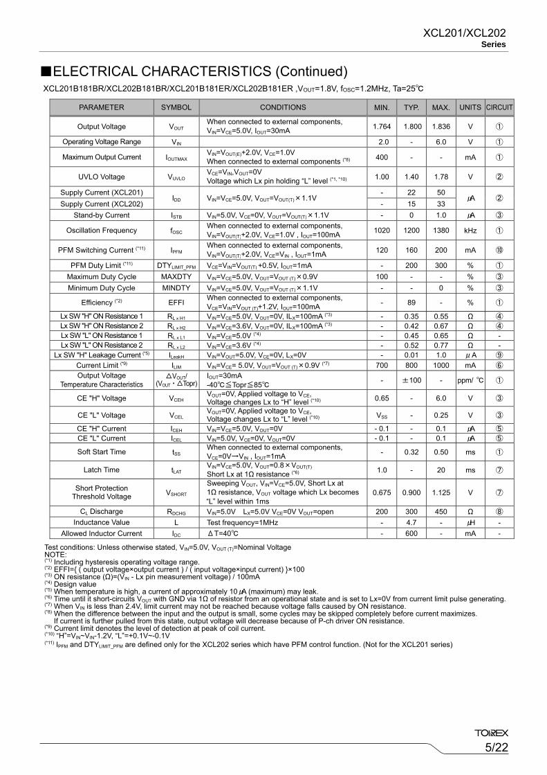
<PFM Switch Current> In PFM control operation, until coil current reaches to a specified level (IPFM), the IC keeps the P-ch MOSFET on. In this case, on-time (tON) that the P-ch MOSFET is kept on can be given by the following formula. tON = L×IPFM / (VIN-VOUT) →IPFM① <PFM Duty Limit> In the PFM control operation, the PFM Duty Limit (DTYLIMIT_PFM) is set to 200% (TYP.). Therefore, under the condition that the duty increases (e.g. the condition that the step-down ratio is small), it’s possible for P-ch MOSFET to be turned off even when coil current doesn’t reach to IPFM. →IPFM②
<CL High Speed Discharge> The XCL201/XCL202 series can quickly discharge the electric charge at the output capacitor (CL) when a low signal to the CE pin which enables a whole IC circuit put into OFF state, is inputted via the N-channel transistor located between the LX pin and the VSS pin. When the IC is disabled, electric charge at the output capacitor (CL) is quickly discharged so that it may avoid application malfunction. Discharge time of the output capacitor (CL) is set by the CL auto-discharge resistance (R) and the output capacitor (CL). By setting time constant of a CL auto-discharge resistance value [R] and an output capacitor value (CL) as τ(τ=C x R), discharge time of the output voltage after discharge via the N channel transistor is calculated by the following formula. V = VOUT(T) x e –t/τ or t=τln (VOUT(T) / V) V : Output voltage after discharge VOUT(T) : Output voltage t: Discharge time, τ: C x R C=Capacitance of output capacitor (CL) R=CL auto-discharge resistance
0
20
40
60
80
100
0 20 40 60 80 100
Discharge Time t(ms)
Outp
ut
Voltag
e (R
ela
tive
Val
ue)
100 =
Sett
ing
Voltag
e V
alue
CL=10μF
CL=20μF
CL=50μF
tON
Lx
IPFM
0mA
IPFM① IPFM②
0mA
Lx fOSC
最大 IPFM 制限
Output Voltage Discharge Characteristics RDCHG=300Ω(TYP.)
ILx ILx IPFM
DTY LIMIT_PFM

10/22
XCL201/XCL202 Series
OPERATIONAL DESCRIPTION (Continued)
<CE Pin Function> The operation of the XCL201/XCL202 series will enter into the shut down mode when a low level signal is input to the CE pin. During the shutdown mode, the current consumption of the IC becomes 0μA (TYP.), with a state of high impedance at the Lx pin and VOUT pin. The IC starts its operation by inputting a high level signal to the CE pin. The input to the CE pin is a CMOS input and the sink current is 0μA (TYP.). XCL20/XCL202 series - Examples of how to use CE pin
<Soft Start> Soft start time is internally set 0.25ms to 0.32ms (TYP). Soft start time is defined as the time to reach 90% of the output nominal voltage when the CE pin is turned on.
FUNCTION CHART
(A)
SW_CE SELECTED STATUS
ON Stand-by OFF Operation
(B)
SW_CE SELECTED STATUS
ON Operation OFF Stand-by
CE OPERATIONAL STATES VOLTAGE
LEVEL XCL201 XCL202
H Level (*1) Synchronous
PWM Fixed Control Synchronous
PWM/PFM Automatic Switching
L Level (*2) Stand-by Stand-by
* CE pin voltage level range (*1) H level: 0.65V<VCE<6V (*2) L level: 0V<VCE<0.25V (*3) CE pin should not be left open to avoid unstable operation.
CE CE
VIN VDD
SW_CE R1
< IC inside > < IC inside >
VINVDD
VCEH
tss
0V
0V
90% of setting voltage
VCE
VOUT

11/22
XCL201/XCL202Series
NOTE ON USE
④
Limit > #ms⑤ ③
②
①
Delay
Lx
ILIM
ILx
1. The XCL201/XCL202 series is designed for use with ceramic output capacitors. If, however, the potential difference is too large between the input voltage and the output voltage, a ceramic capacitor may fail to absorb the resulting high switching energy and oscillation could occur on the output. If the input-output potential difference is large, connect an electrolytic capacitor in parallel to compensate for insufficient capacitance.
2. Spike noise and ripple voltage arise in a switching regulator as with a DC/DC converter. These are greatly influenced by external
component selection, such as the coil inductance, capacitance values, and board layout of external components. Once the design has been completed, verification with actual components should be done.
3. Depending on the input-output voltage differential, or load current, some pulses may be skipped, and the ripple voltage may increase. 4. When the difference between input and output is large in PWM control, very narrow pulses will be outputted, and there is the possibility
that some cycles may be skipped completely. 5. When the difference between input and output is small, and the load current is heavy, very wide pulses will be outputted and there is the
possibility that some cycles may be skipped completely. 6. With the IC, the peak current of the coil is controlled by the current limit circuit. Since the peak current increases when dropout voltage or
load current is high, current limit starts operation, and this can lead to instability. When peak current becomes high, please adjust the coil inductance value and fully check the circuit operation. In addition, please calculate the peak current according to the following formula:
Ipk = (VIN - VOUT) x OnDuty / (2 x L x fOSC) + IOUT L: Coil Inductance Value fOSC: Oscillation Frequency
7. When the peak current which exceeds limit current flows within the specified time, the built-in P-ch driver transistor turns off. During the
time until it detects limit current and before the built-in transistor can be turned off, the current for limit current flows; therefore, care must be taken when selecting the rating for the external components such as a coil.
8. When VIN is less than 2.4V, limit current may not be reached because voltage falls caused by ON resistance. 9. Depending on the state of the PC Board, latch time may become longer and latch operation may not work. In order to avoid the effect of
noise, the board should be laid out so that input capacitors are placed as close to the IC as possible. 10. Use of the IC at voltages below the recommended voltage range may lead to instability. 11. This IC should be used within the stated absolute maximum ratings in order to prevent damage to the device. 12. When the IC is used in high temperature, output voltage may increase up to input voltage level at no load because of the leak current of
the driver transistor. 13. The current limit is set to 1000mA (MAX.) at typical. However, the current of 1000mA or more may flow.
In case that the current limit functions while the VOUT pin is shorted to the GND pin, when P-ch MOSFET is ON, the potential difference for input voltage will occur at both ends of a coil. For this, the time rate of coil current becomes large. By contrast, when N-ch MOSFET is ON, there is almost no potential difference at both ends of the coil since the VOUT pin is shorted to the GND pin. Consequently, the time rate of coil current becomes quite small. According to the repetition of this operation, and the delay time of the circuit, coil current will be converged on a certain current value, exceeding the amount of current, which is supposed to be limited originally. Even in this case, however, after the over current state continues for several ms, the circuit will be latched. A coil should be used within the stated absolute maximum rating in order to prevent damage to the device.
①Current flows into P-ch MOSFET to reach the current limit (ILIM). ②The current of ILIM or more flows since the delay time of the circuit occurs during from the detection of the current limit to OFF of P-ch MOSFET. ③Because of no potential difference at both ends of the coil, the time rate of coil current becomes quite small. ④Lx oscillates very narrow pulses by the current limit for several ms. ⑤The circuit is latched, stopping its operation.

12/22
XCL201/XCL202 Series
NOTE ON USE (Continued)
the power loss of micro DC/DC according to the following formula:
power loss = VOUT×IOUT×((100/EFFI) – 1) (W) VOUT : Output Voltage (V) IOUT : Output Current (A) EFFI: Conversion Efficiency (%)
Measurement Condition (Reference data) Condition: Mount on a board
Ambient: Natural convection
Soldering: Lead (Pb) free
Board: Dimensions 40 x 40 mm (1600 mm2 in one side) Copper (Cu) traces occupy 50% of the board area
In top and back faces
Package heat-sink is tied to the copper traces
Material: Glass Epoxy (FR-4)
Thickness: 1.6mm
Through-hole: 4 x 0.8 Diameter
14. In order to stabilize VIN voltage level and oscillation frequency, we recommend that a by-pass capacitor (CIN) be connected as close as possible to the VIN & VSS pins.
15. High step-down ratio and very light load may lead an intermittent oscillation when PWM mode. 16. When PWM/PFM automatic switching goes into continuous mode, the IC may be in unstable operation for the range of MAXDUTY area
with small input/output differential. 17. Please use within the power dissipation range below. Please also note that the power dissipation may changed by test conditions, the
power dissipation figure shown is PCB mounted.
Evaluation Board (unit: mm)
Pd vs Operating Temperature Pakage Body Temperature vs Operating Temperature

13/22
XCL201/XCL202Series
NOTE ON USE (Continued) Instructions of pattern layouts 1. In order to stabilize VIN voltage level, we recommend that a by-pass capacitor (CIN) be connected as close as possible to the VIN (No.6) & VSS
(No.5) pins. 2. Please mount each external component as close to the IC as possible. 3. Wire external components as close to the IC as possible and use thick, short connecting traces to reduce the circuit impedance. 4. Make sure that the PCB GND traces are as thick as possible, as variations in ground potential caused by high ground currents at the time of
switching may result in instability of the IC. 5. This series’ internal driver transistors bring on heat because of the output current and ON resistance of driver transistors. 6. Please connect Lx (No.1) pin and L1 (No.7) pin by wiring on the PCB. 7. Please connect VOUT (No.3) pin and L2 (No.8) pin by wiring on the PCB.
CIN
CL
IC
LX
VINGND
GNDVOUT
CE
CIN
CL
IC
LX
VINGND
GNDVOUT
CE
CE LX
VINGND
GNDVOUT
BACK (Flip Horizontal)
FRONT (PCB mounted)
FRONT

14/22
XCL201/XCL202 Series
TEST CIRCUITS
* External Components L: 4.7μH (Screening Parts) CIN: 4.7μF (Ceramic) CL: 10μF (Ceramic)
* External Components CIN: 4.7μF (Ceramic) CL: 10μF (Ceramic)

15/22
XCL201/XCL202Series
TYPICAL PERFORMANCE CHARACTERISTICS (1) Efficiency vs. Output Current (2) Output Voltage vs. Output Current
(3) Ripple Voltage vs. Output Current (4) Oscillation Frequency vs. Ambient Temperature
(5) Supply Current vs. Ambient Temperature (6) Output Voltage vs. Ambient Temperature
0
20
40
60
80
100
0.01 0.1 1 10 100 1000
Output Current:IOUT (mA)
Effic
ency
:EFF
I(%)
3.6V
XCL202(PWM/PFM)
XCL201(PWM)
2.7V
VIN= 4.2V
1.5
1.6
1.7
1.8
1.9
2.0
2.1
0.01 0.1 1 10 100 1000
Output Current:IOUT (mA)O
utpu
t Vol
tage
:VO
UT(
V)
VIN=4.2V,3.6V,2.7V
XCL201
(PWM/PFM)
(PWM)
XCL202
0
20
40
60
80
100
0.01 0.1 1 10 100 1000
Output Current:IOUT (mA)
Rip
ple
Volta
ge:V
r(m
V)
3.6VXCL201
XCL202
VIN=4.2V
2.7V VIN=4.2V 3.6V
2.7V
(PWM/PFM)
(PWM)
0.8
0.9
1.0
1.1
1.2
1.3
1.4
1.5
-50 -25 0 25 50 75 100
Ambient Temperature: Ta ()
VIN=3.6V
Osc
illatio
n Fr
eque
ncy
: fos
c(M
Hz)
0
5
10
15
20
25
30
35
40
-50 -25 0 25 50 75 100
Ambient Temperature: Ta ()
Supp
ly C
urre
nt :
I DD (μ
A)
VIN=6.0V4.0V
2.0V
1.5
1.6
1.7
1.8
1.9
2.0
2.1
-50 -25 0 25 50 75 100
Ambient Temperature: Ta ()
Out
put V
olta
ge :
VO
UT
(V)
VIN=3.6V
XCL201B181BR/XCL202B181BR XCL201B181BR/XCL202B181BR
XCL201B181BR/XCL202B181BR XCL201B181BR/XCL202B181BR
XCL202B181BR XCL201B181BR/XCL202B181BR

16/22
XCL201/XCL202 Series
TYPICAL PERFORMANCE CHARACTERISTICS (Continued) (7) UVLO Voltage vs. Ambient Temperature (8) CE "H" Voltage vs. Ambient Temperature
(9) CE "L" Voltage vs. Ambient Temperature (10) "Pch / Nch" Driver on Resistance vs. Input Voltage
(11) Rise Wave Form
0.0
0.3
0.6
0.9
1.2
1.5
1.8
-50 -25 0 25 50 75 100
Ambient Temperature: Ta ()
UVL
O V
olta
ge :
UVL
O (V
)
CE=VIN
0.0
0.1
0.2
0.3
0.4
0.5
0.6
0.7
0.8
0.9
1.0
-50 -25 0 25 50 75 100
Ambient Temperature: Ta ()C
E "H
" Vol
tage
: V C
EH (V
) VIN=5.0V
3.6V
2.4V
0.0
0.1
0.2
0.3
0.4
0.5
0.6
0.7
0.8
0.9
1.0
-50 -25 0 25 50 75 100
Ambient Temperature: Ta ()
CE
"L" V
olta
ge :
V CEL
(V)
VIN=5.0V
3.6V
2.4V
0.0
0.1
0.2
0.3
0.4
0.5
0.6
0.7
0.8
0.9
1.0
0 1 2 3 4 5 6
Input Voltage : VIN (V)
Pch on Resistance
Nch on Resistance
Lx S
W O
N R
esis
tanc
e:R
LxH
,RLx
L (Ω
)
CE:0.0V⇒1.0V
VIN=5.0VIOUT=1.0mA
Time:100μs/div
VOUT
1ch
2ch
1ch:1V/div 2ch:1V/div
XCL201B331BR/XCL202B331BR
XCL201B181BR/XCL202B181BR XCL201B181BR/XCL202B181BR
XCL201B181BR/XCL202B181BR XCL201B181BR/XCL202B181BR

17/22
XCL201/XCL202Series
TYPICAL PERFORMANCE CHARACTERISTICS (Continued) (12) Soft-Start Time vs. Ambient Temperature (13) CL Discharge Resistance vs. Ambient Temperature
(14) Load Transient Response MODE:PWM/PFM Automatic Switching Control
0
100
200
300
400
500
-50 -25 0 25 50 75 100
Ambient Temperature: Ta ()
VIN=5.0VIOUT=1.0mA
Soft
Star
t Tim
e : t
ss (μ
s)
100
200
300
400
500
600
-50 -25 0 25 50 75 100
Ambient Temperature: Ta ()C
L D
isch
arge
Res
ista
nce:
(Ω)
VIN=6.0V
4.0V
2.0V
XCL201B121BR/XCL202B121BR XCL201B331BR/XCL202B331BR
XCL202B181BR XCL202B181BR
XCL202B181BR XCL202B181BR

18/22
XCL201/XCL202 Series
TYPICAL PERFORMANCE CHARACTERISTICS (Continued) (14) Load Transient Response (Continued)
MODE:PWM Control
XCL201B181BR XCL201B181BR
XCL201B181BR XCL201B181BR

19/22
XCL201/XCL202Series
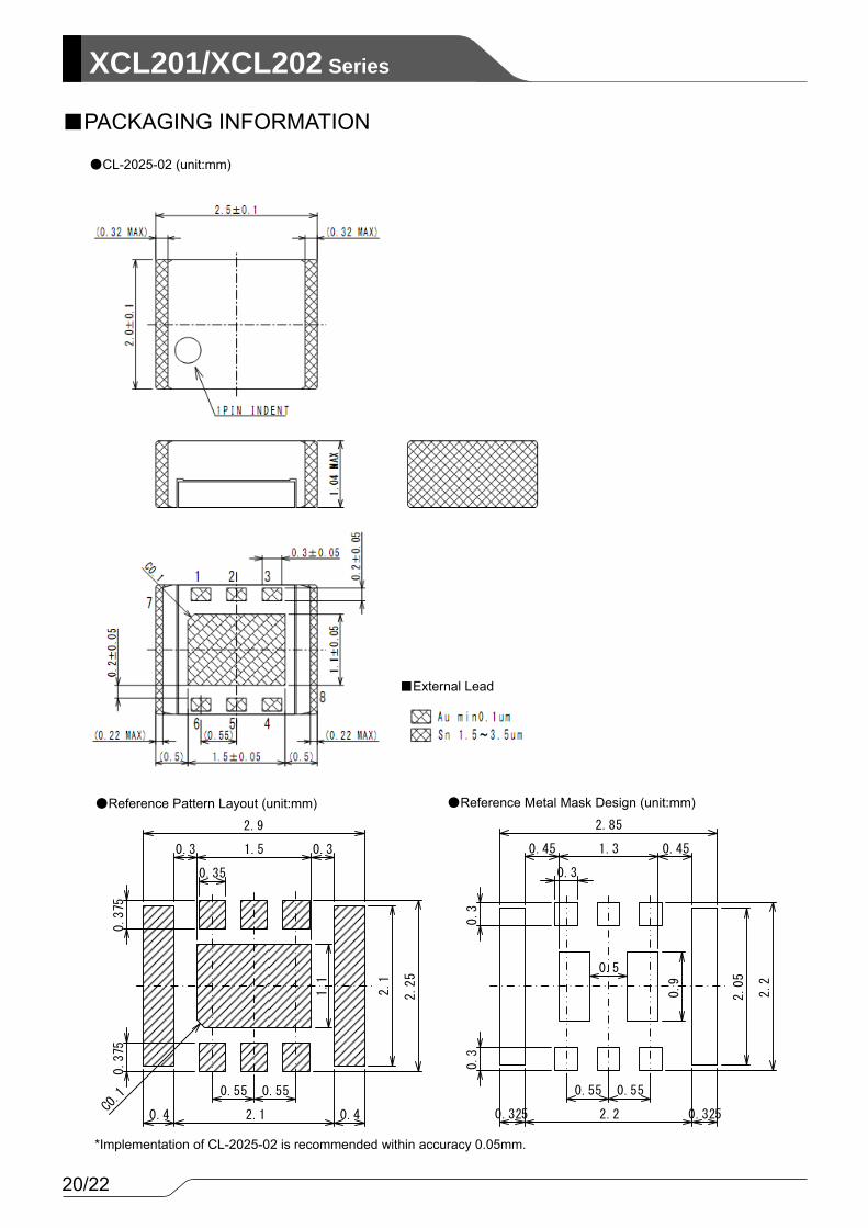
PACKAGING INFORMATION
CL-2025 (unit:mm)
Reference Pattern Layout (unit:mm) Reference Metal Mask Design (unit:mm)
External Lead
20/22
XCL201/XCL202 Series
PACKAGING INFORMATION
Reference Metal Mask Design (unit:mm)
CL-2025-02 (unit:mm)
Reference Pattern Layout (unit:mm)
External Lead
*Implementation of CL-2025-02 is recommended within accuracy 0.05mm.
0.3
2.9
1.5 0.30.3
0.35
0.375
0.375
0.4 2.1 0.4
0.55 0.55
1.1
2.1
2.25
2.85
1.30.45 0.45
0.3
0.5
0.9
2.05
2.2
2.20.325 0.325
0.3
0.55 0.55

21/22
XCL201/XCL202Series
MARKING RULE
① represents products series
② represents integer of output voltage and oscillation frequency
③ represents the decimal part of output voltage
Example (Mark ②, ③)
④,⑤ represents production lot number 01~09, 0A~0Z, 11~9Z, A1~A9, AA~AZ, B1~ZZ in order.
(G, I, J, O, Q, W excluded) *No character inversion used.
MARK PRODUCT SERIES
F XCL201B*****-G H XCL202B*****-G
OUTPUT VOLTAGE (V) MARK
OSCILLATION FREQUENCY=1.2MHz (XCL20****1**-G)
0.x F 1.x H 2.x K 3.x L 4.x M
OUTPUT VOLTAGE (V) MARK PRODUCT SERIES
X.0 0 XCL20***0***-G X.05 A XCL20***A***-G X.1 1 XCL20***1***-G
X.15 B XCL20***B***-G X.2 2 XCL20***2***-G
X.25 C XCL20***C***-G X.3 3 XCL20***3***-G
X.35 D XCL20***D***-G X.4 4 XCL20***4***-G
X.45 E XCL20***E***-G X.5 5 XCL20***5***-G
X.55 F XCL20***F***-G X.6 6 XCL20***6***-G
X.65 H XCL20***H***-G X.7 7 XCL20***7***-G
X.75 K XCL20***K***-G X.8 8 XCL20***8***-G
X.85 L XCL20***L***-G X.9 9 XCL20***9***-G
X.95 M XCL20***M***-G
OSCILLATION FREQUENCY
MARK
XCL20**33***-G XCL20**2C***-G XCL20**1L***-G② ③ ② ③ ② ③
1.2MHz L 3 K C H L
⑤④
①②
1
2
3
6
5
4
③
CL-2025/CL-2025-02
22/22
XCL201/XCL202 Series
1. The product and product specifications contained herein are subject to change without notice to improve performance characteristics. Consult us, or our representatives before use, to confirm that the information in this datasheet is up to date.
2. The information in this datasheet is intended to illustrate the operation and characteristics of our
products. We neither make warranties or representations with respect to the accuracy or completeness of the information contained in this datasheet nor grant any license to any intellectual property rights of ours or any third party concerning with the information in this datasheet.
3. Applicable export control laws and regulations should be complied and the procedures required by
such laws and regulations should also be followed, when the product or any information contained in this datasheet is exported.
4. The product is neither intended nor warranted for use in equipment of systems which require
extremely high levels of quality and/or reliability and/or a malfunction or failure which may cause loss of human life, bodily injury, serious property damage including but not limited to devices or equipment used in 1) nuclear facilities, 2) aerospace industry, 3) medical facilities, 4) automobile industry and other transportation industry and 5) safety devices and safety equipment to control combustions and explosions. Do not use the product for the above use unless agreed by us in writing in advance.
5. Although we make continuous efforts to improve the quality and reliability of our products;
nevertheless Semiconductors are likely to fail with a certain probability. So in order to prevent personal injury and/or property damage resulting from such failure, customers are required to incorporate adequate safety measures in their designs, such as system fail safes, redundancy and fire prevention features.
6. Our products are not designed to be Radiation-resistant.
7. Please use the product listed in this datasheet within the specified ranges.
8. We assume no responsibility for damage or loss due to abnormal use.
9. All rights reserved. No part of this datasheet may be copied or reproduced unless agreed by Torex
Semiconductor Ltd in writing in advance.
TOREX SEMICONDUCTOR LTD.