Embed Size (px)
Citation preview

XC878 series
8-bit microcontrollers with 64K Flash and CAN connectivity
New member to cost-effective XC800 8-bit Family
July 2008

Page 2Copyright © Infineon Technologies 2007. All rights reserved. 28.06.2007
Agenda
XC878 Product Presentation (Technical Overview)Family OverviewSystem & CoreEmbedded MemoriesStandard Peripherals ¬ GPIO ¬ Timers & WDT ¬ UART & LIN ¬ SSC
Special Peripherals¬ ADC¬ CAPCOM6E¬ T2CCU¬ MultiCAN¬ MDU & Cordic
Debug Support & Toolchain

Page 3Copyright © Infineon Technologies 2007. All rights reserved. 28.06.2007
Roadmap for XC800 Family

Page 4Copyright © Infineon Technologies 2007. All rights reserved. 28.06.2007
New XC878 Series on a Glance
Identify which feature is most important to the customers listed above
ApplicationsAutomotive Body: Power Closure Systems, Steering lock , ImmobilizersMotor Control: Air conditioners, White goods, Forklifts, AutomationBuilding control: Compressors, pumps, Fans, LED lighting
Advantage Advanced peripheral integration for motor control performance FOC + PFC on a single MCU together with CAN connectivity
Key Benefits to Customers
64KB Flash, 3KB RAM and CAN connectivityPowerful motor control features: Vector Computer, ADC ,CCU6E 2 PWM timers with 8 PWM channels and 4 independent time basesIntegrated safety features: Voltage &Clock supervisory, ECC
Eval Boards XC878 Easy Kit €99

Page 5Copyright © Infineon Technologies 2007. All rights reserved. 28.06.2007
XC878 Product Block Diagram
64KB Flash, 3KB RAM and CAN connectivityPowerful motor control features: Vector Computer, ADC ,CCU6E
Enables Field Oriented Control at lowest system cost
2 PWM Modules with 10 PWM channels and 4 independent time basesEnables PFC + FOC motor control on a single MCU
Integrated safety features: Voltage & Clock supervisory, ECC
Supporting Documentationwww.infineon.com/XC878
– AppNotes– Data Sheets– Users Manual– Hands On Training

Page 6Copyright © Infineon Technologies 2007. All rights reserved. 28.06.2007
Pin-Out Compatibility within XC800 Family
LQFP64 and TSSOP38LQFP64 and LQFP48
LQFP487.0 x 7.0
LQFP6410.0 x 10.0
TSSOP389.7 x 4.4 TSSOP20
6.5 x 4.4
0.5mm 0.65mm
Body Size
Pin Pitch
XC878 and XC888

Page 7Copyright © Infineon Technologies 2007. All rights reserved. 28.06.2007
Migration from XC886/888 to XC878
Migration guide is available Starterkit CDList of differences:
Memory ExtensionFlash ArchitectureClock SystemEVR and InterruptsBootstrap LoaderPinout
Note: Actual Starter Kit CD contents is available on www.infineon.com\xc878

Page 8Copyright © Infineon Technologies 2007. All rights reserved. 28.06.2007
Agenda
XC878 Product Presentation (Technical Overview)Family OverviewSystem & CoreEmbedded MemoriesStandard Peripherals ¬ GPIO ¬ Timers & WDT ¬ UART & LIN ¬ SSC
Special Peripherals¬ ADC¬ CAPCOM6E¬ T2CCU¬ MultiCAN¬ MDU & Cordic
Debug Support & Toolchain
Page 9Copyright © Infineon Technologies 2007. All rights reserved. 28.06.2007
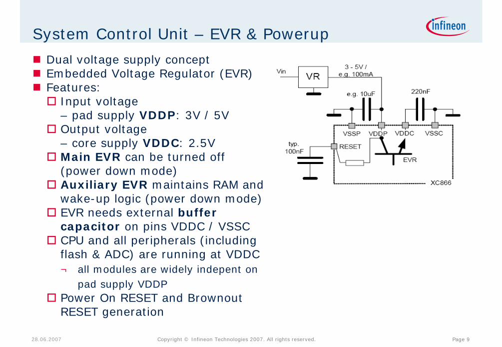
System Control Unit – EVR & Powerup
Dual voltage supply conceptEmbedded Voltage Regulator (EVR) Features:
Input voltage – pad supply VDDP: 3V / 5VOutput voltage – core supply VDDC: 2.5V Main EVR can be turned off (power down mode)Auxiliary EVR maintains RAM and wake-up logic (power down mode)EVR needs external buffer capacitor on pins VDDC / VSSCCPU and all peripherals (including flash & ADC) are running at VDDC¬ all modules are widely indepent on
pad supply VDDPPower On RESET and Brownout RESET generation
Page 10Copyright © Infineon Technologies 2007. All rights reserved. 28.06.2007
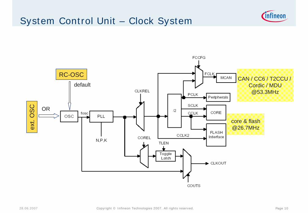
System Control Unit – Clock System
RC-OSC
ext.
OS
C OR
defaultCAN / CC6 / T2CCU /
Cordic / [email protected]
core & [email protected]

Page 11Copyright © Infineon Technologies 2007. All rights reserved. 28.06.2007
System Control Unit – Interrupt Controller
Interrupt Controller14 interrupt vectors with four priority levels¬ up to 15 external
interruptsNon-Maskable interrupt (NMI); highest priority

Page 12Copyright © Infineon Technologies 2007. All rights reserved. 28.06.2007
System Control Unit – Power ManagementFour Power Management Modes
Active Mode ¬ peripherals can be
individually enabled/disabledIdle Mode¬ CPU is off and wakes up on
any interruptSlowdown Mode¬ CPU and all modules are
clocked down ¬ prescaler /1, /2, /3, /4, /5,
/8, etc...Powerdown Mode¬ CPU and all peripherals are
clockless¬ main EVR is off¬ wakeuplogic active¬ RAM/SFRs keep value¬ wakeup thru EXINT0 or
RESET
~10uA@25°CPower Down
~9mASlow Down (fsys/2048)
~29mAIdle
~37mAActive
Typical currentconsumption
Mode

Page 13Copyright © Infineon Technologies 2007. All rights reserved. 28.06.2007
System Control Unit – Fail Safe
XC878 provides Hardware functions to meet Safety standards:Class B, Class C, IEC 60730

Page 14Copyright © Infineon Technologies 2007. All rights reserved. 28.06.2007
Boot-Concept
BSL is enteredwith MBC = 0 (always)with MBC = 1 (if flash @0x0000 is zero)
Booting only on pinsP1.0/RXD/RXDC0_0P1.1/TXD/TXDC0_0
Booting always supports autobaudrate detectionMultiCan Booting
point-to-point connectionexternal clock required¬ default 8MHz (initial programming)
x
x
„CM“
--xCAN
-x-LIN
x-xUART
„ - “„L“„C“Mark
Boot
jumps to user definedFlash address
ALTERNATE
download to XRAMCAN
LIN
download to XRAM or Flash
UART
Bootstrap Loader Options

Page 15Copyright © Infineon Technologies 2007. All rights reserved. 28.06.2007
Agenda
XC878 Product Presentation (Technical Overview)Family OverviewSystem & CoreEmbedded MemoriesStandard Peripherals ¬ GPIO ¬ Timers & WDT ¬ UART & LIN ¬ SSC
Special Peripherals¬ ADC¬ CAPCOM6E¬ T2CCU¬ MultiCAN¬ MDU & Cordic
Debug Support & Toolchain

Page 16Copyright © Infineon Technologies 2007. All rights reserved. 28.06.2007
Memory LayoutXC878 – 13FF (52K flash)
compatible to XC886XC878 – 16FF (64K flash)
banking for XRAM
64k
64k
3k XRAM
@ 0xF000
Bank 0
MEX3 = 0
3k XRAM
@ 0xF000
Bank 16
MEX3 = 0x1F

Page 17Copyright © Infineon Technologies 2007. All rights reserved. 28.06.2007
4-KByte block of flash memory(D-Flash) used for
emulation of EEPROM data
60-KByte block of flash memory(P-Flash) used
for code or constant data
Memory Layout – Flash

Page 18Copyright © Infineon Technologies 2007. All rights reserved. 28.06.2007
Flash ArchitectureXC878 has two independent Flash-Blocks:
PFLASH (48/60k) & DFLASH (4k)¬ both can be used for CODE and DATA¬ but DFLASH is capable for „background EEPROM emulation“for data integrity a hardware error correction (ECC) is providedFlash Readout- and Write-Protection mechanism
Characteristics for Programming & Erase:
200msMass Erase Time
4k60kMax Erase Width
64 Bytes512 BytesMin Erase Width
32 Bytes64 BytesMax Programming Width
1 Byte
20ms
20-40us
PFLASH
Min Programming Width
Page Erase Time
Programming Time
DFLASH

Page 19Copyright © Infineon Technologies 2007. All rights reserved. 28.06.2007
Flash Retention & Endurance
Characteristics for Retention & Endurance for DFLASH:
Automotive
emulation mode usingdataset size of 128bytes
5122120k
2048130k
10k
1k
Endurance[cycles]
2
5
15
Retention[years]
512
1024
4096
Size[bytes]
non-emulated
Remark
Industrial
40961100k
30k
10k
1k
Endurance[cycles]
5
10
15
Retention[years]
4096
4096
4096
Size[bytes]
non-emulated
Remark

Page 20Copyright © Infineon Technologies 2007. All rights reserved. 28.06.2007
Agenda
XC878 Product Presentation (Technical Overview)Family OverviewSystem & CoreEmbedded MemoriesStandard Peripherals ¬ GPIO ¬ Timers & WDT ¬ UART & LIN ¬ SSC
Special Peripherals¬ ADC¬ CAPCOM6E¬ T2CCU¬ MultiCAN¬ MDU & Cordic
Debug Support & Toolchain

Page 21Copyright © Infineon Technologies 2007. All rights reserved. 28.06.2007
GPIO
Flexible IO configuration
Two driver strength
Open drain mode
Selectable pullup/down devices
Up to 4 alternate output functions on each I/O
Up to 15 external interrupts on different nodes

Page 22Copyright © Infineon Technologies 2007. All rights reserved. 28.06.2007
Timers T0, T1
Incremented once every fsys / 2Timer Modes
Mode 0: 13-bit timerMode 1: 16-bit timerMode 2: 8-bit timer with auto-reloadMode 3; T0 is configured as two 8-bit timers. T1 holds the count.external counter modetwo interrupt vectors for T0 / T1

Page 23Copyright © Infineon Technologies 2007. All rights reserved. 28.06.2007
Timers T2, T21
T2 / T21 have same functionality16bit up/down-count withautoreloadcapture – T2EXexternal start – T2EXoutput toggle – EXF2external count input – T2
large prescaler arrangementsupports automatic baudratecapture for UART/UART1two interrupt vectors on sharednodes

Page 24Copyright © Infineon Technologies 2007. All rights reserved. 28.06.2007
Watchdog TimerWindow Watchog Timer
Provides a reliable and secure way to detect and recover from SW or HW failures
If the WDT is not serviced (refreshed) within the allowed window a system malfunction is assumed and an internal RESET is performedThe window can be freely programmed

Page 25Copyright © Infineon Technologies 2007. All rights reserved. 28.06.2007
UART / UART1
Two independent UART modulesFull DuplexReceive Double Buffered8/9-bit UART with a variable baud rateIntegrated Baudrate GeneratorIntegrated Fractional Divider for accurate baudrate adjustmentAutobaudrate capture feature for LIN2.0 headerTwo interrupt vectors for UART/UART1

Page 26Copyright © Infineon Technologies 2007. All rights reserved. 28.06.2007
SSC
High Speed Synchronous Serial InterfaceSupports both full-duplex and half-duplex serial synchronous communication up to 13.3 MBaudSerial clock signal can be generated by the SSC (in Master mode) or can be received from an external master (Slave mode).Transmission and reception is double-buffered.A 16-bit baud-rate generator provides a separate clock signal.Communication with SPI compatible devices is supportedFlexible data format¬ Programmable number of data bits: 2 to 8 bits¬ Programmable shift direction: LSB or MSB shift first¬ Programmable clock polarity: idle low or high state for the shift
clock¬ Programmable clock/data phase: data shift with leading or
trailing edge of the shift clock.Interrupt generation¬ On a transmitter empty condition¬ On a receiver full condition¬ On an error condition (receive, phase, baud rate, transmit error)

Page 27Copyright © Infineon Technologies 2007. All rights reserved. 28.06.2007
Agenda
XC878 Product Presentation (Technical Overview)Family OverviewSystem & CoreEmbedded MemoriesStandard Peripherals ¬ GPIO ¬ Timers & WDT ¬ UART & LIN ¬ SSC
Special Peripherals¬ ADC¬ CAPCOM6E¬ T2CCU¬ MultiCAN¬ MDU & Cordic
Debug Support & Toolchain

Page 28Copyright © Infineon Technologies 2007. All rights reserved. 28.06.2007
ADC
ADC – Block Diagram
Result 0
Result 1
Result 2
Result 3
ChannelControl
InterruptGeneration
RequestSources
RequestControl
Con-verter
ResultControl
Result Assignment
Sample Time Adjust
Autoscan
Cancel- Inject -Repeat
8 / 9/ 10 / 11 bitlimit checker
SequenceTimer
Software
analog digital

Page 29Copyright © Infineon Technologies 2007. All rights reserved. 28.06.2007
ADC – Features
ADC Characteristics8 channels with 10bit resolutionTUE = +/- 3 lsb, DNLE = +/- 2 lsb, INLE = +/- 2 lsbsample time down to 75nsconversion time down to 0.85us@8bit and 1us@10bit
ADC FeaturesFully autonomous peripheral which off loads CPU whileconverting¬ ADC triggering and result storage is solved in hardware¬ background conversions in a defined sequence are possible¬ limit & boundary checking with interrupt (comparator mode)¬ autoscan and queued conversion on several channels¬ result accumulator & data reduction filter (median filter)¬ timetriggered and injected conversions (hardware arbitration)¬ 8, 9, 10, 11 bits result
more details on Starterkit CD

Page 30Copyright © Infineon Technologies 2007. All rights reserved. 28.06.2007
ADC– Limit and Boundary Checking
Reduced CPU loadSoftware interaction for interesting results only
Reduced CPU loadSoftware interaction for interesting results only
• comparator mode is selective per channel
• limit is global forall channels
• 4bits for upper & lower limit
• 8 combinationswith 3 areas
Comparator ModeComparator Mode
Page 31Copyright © Infineon Technologies 2007. All rights reserved. 28.06.2007
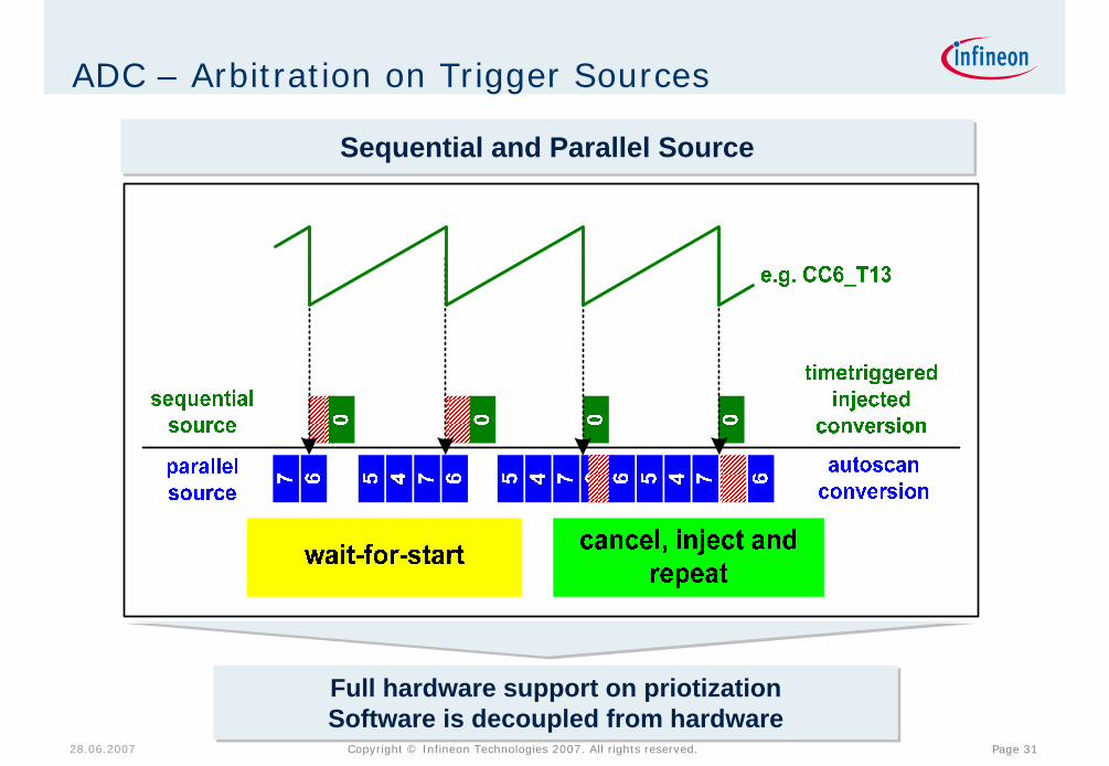
ADC – Arbitration on Trigger Sources
Sequential and Parallel SourceSequential and Parallel Source
Full hardware support on priotizationSoftware is decoupled from hardwareFull hardware support on priotizationSoftware is decoupled from hardware

Page 32Copyright © Infineon Technologies 2007. All rights reserved. 28.06.2007
CAPCOM6ECAPCOM6E – Block Diagram

Page 33Copyright © Infineon Technologies 2007. All rights reserved. 28.06.2007
CAPCOM6E
Timer 12 featuresThree capture/compare channels (each can be used as capture or as compare)Supports generation of a three-phase PWM16-bit resolutionDead-time control for each channel (avoid short-circuits in power stage)Concurrent update of the required T12/T13 registersCenter aligned and edge aligned PWMSingle shot modeHysteresis-like control modeHall-mode for multiphase BLDC motors
Timer 13 featuresOne independent compare channel with one output16-bit resolutionCan be sychonized to T12Interrupt generation at period-match and compare-matchSingle-shot mode supported

Page 34Copyright © Infineon Technologies 2007. All rights reserved. 28.06.2007
CAPCOM6E
Additional Features
Block commutation for Brushless DC-drives implementedPosition detection via Hall-sensor patternAutomatic rotational speed measurement for block commutationIntegrated error handlingFast emergency stop with CPU load via external signal (CTRAP)Control modes for multi-channel AC-drivesOutput levels can be selected and adapted to the power stage
Module InterfaceT12 and T13 can be started from external pin (T12HR, T13HR)ADC can be synchronized on ¬ T12PM¬ T12CM0,1,2¬ T13PM¬ T13CM¬ STR¬ CHE

Page 35Copyright © Infineon Technologies 2007. All rights reserved. 28.06.2007
Mode
T12T12
Capture/Compare Timer 16-bit
Period RegisterPeriod Register CTRAP
CC0 COUT0CC1 COUT1CC2 COUT2
FCPU
CC Channel 0 CC0CC Channel 0 CC0
CC Channel 1 CC1CC Channel 1 CC1
CC Channel 2 CC2CC Channel 2 CC2
deadtimeControl
T13 Compare Timer 16-bitFCPU
Period Reg. Period Reg.
Comp Reg. CC3Comp Reg. CC3
Burst Mode
BlockCommutation
Control
COUT3
INT0INT1INT2 MM
Port
Cont
rol L
ogic
CAPCOM6E – FOC of BLDC MotorsT12 Generates Symmetric PWM with Dead-TimeT13 in single shot mode and synchronized to T12 generates 2 A/D Triggers for current measurement
T12Capture/Compare
Timer 16-bit
T12
deadtimeControl
Port
Cont
rol L
ogicCC Channel 0 CC0CC Channel 0 CC0
CC Channel 1 CC1CC Channel 1 CC1
CC Channel 2 CC2CC Channel 2 CC2
Compare RegisterCompare Register
Period Register Period Register
A/D Triggers
Period Register

Page 36Copyright © Infineon Technologies 2007. All rights reserved. 28.06.2007
CAPCOM6E – BLDC Motors with Hall Sensors
Mode
T12T12
Capture/Compare Timer 16-bit
Period RegisterPeriod Register CTRAP
CC0 COUT0CC1 COUT1CC2 COUT2
FCPU
CC Channel 0 CC0CC Channel 0 CC0
CC Channel 1 CC1CC Channel 1 CC1
CC Channel 2 CC2CC Channel 2 CC2
deadtimeControl
T13Compare Timer
16-bitFCPU
Period Reg. Period Reg.
Comp Reg. CMP2Comp Reg. CMP2
Burst Mode
BlockCommutation
Control
COUT3
INT0INT1INT2
Port
Cont
rol L
ogic
T13Compare Timer
16-bit
BlockCommutation
Control
Port
Cont
rol L
ogic
Period Register
Comp RegisterComp Register
SpeedSpeed
Phase DelayPhase Delay
Time Out (Stall Detect)Time Out (Stall Detect)
Hall EffectNoise FilterHall EffectNoise Filter
T12Capture/Compare
Timer 16-bit
T12Capture/Compare
Timer 16-bit
A/D TriggerHall EffectSensors
more details on Starterkit CD

Page 37Copyright © Infineon Technologies 2007. All rights reserved. 28.06.2007
T2CCU – OverviewT2CCU is a simplifiedCapture/Compare Unit
one 16bit autoreload timerwhich counts upprogrammable reloadvalueinterrupt on overflow6 independent capcomchannels interrupttwo selectable time baseunits: CCT or T2clock prescaler options up to ft2ccu = 2x fcpu(48MHz)synchronize features forCCT & T2ADC trigger features
Page 38Copyright © Infineon Technologies 2007. All rights reserved. 28.06.2007
T2CCU – Applications
T2CCU can be used forstepper motor control (full-/half-/microstep)6 channel PWM generation (e.g. LED control)3 phase PWM with deadtime (motor control, PFC, lampballast)multiple trigger pulses (e.g. for valve control) capturing external events

Page 39Copyright © Infineon Technologies 2007. All rights reserved. 28.06.2007
T2CCU – PWM Generation
Compare Mode 0:output change (set / reset) on ¬ compare and overflowup to 6 channels2 can be combined with PolA/B and deadtime for 3 phase halfbridgecontrol
shadow transfer mechanism forcompare value update
update compare channelsset TXOFclear TXOFcompare value is active with nexttimer overflow
note: compare value must not besmaller than reload value

Page 40Copyright © Infineon Technologies 2007. All rights reserved. 28.06.2007
T2CCU – Pulse Pattern Generation
Compare Mode 1:use this mode for flexible pulse pattern generationuse TXOF for timersynchronous update forshadow transfer of all compare values

Page 41Copyright © Infineon Technologies 2007. All rights reserved. 28.06.2007
T2CCU – Stepper Motor Control
Concurrent Compare Mode:¬ similar to Compare Mode 1 but only Compare 0 register has to be written
Stepper Motor Controlfullstep / halfstep modetimer period refers to speedequidistant compare values
use ENSHDW to update nextcompare valuepattern & time schedule table canbe usednote: realtime update is mandatory

Page 42Copyright © Infineon Technologies 2007. All rights reserved. 28.06.2007
T2CCU – Capturing External Events
Capture Modes :capture external events on ¬ rising / falling / both edgessoft-capture – read actualtimervalueindividual interrupt flags forevery capture event
note: take care on timeroverflow while capturing
more details on Starterkit CD

Page 43Copyright © Infineon Technologies 2007. All rights reserved. 28.06.2007
MultiCAN
ISO 11898 compliant CAN module (V2.0B active)2 independent CAN nodes, with dedicated control registers for each CAN node32 independent message objectswith acceptance mask filtering for each MOData transfer rate up to 1MBaudFlexible and powerful message transfer control (double chained list) and error handling capabilities to offload CPUAutomatic gateway mode supportCAN Analyzer Mode for bus monitoring

Page 44Copyright © Infineon Technologies 2007. All rights reserved. 28.06.2007
Certificategranted
CAN Conformance testfor XC88xC passedCAN Gateway test passed
MultiCAN Module Conformance Test
more details on Starterkit CD

Page 45Copyright © Infineon Technologies 2007. All rights reserved. 28.06.2007
Coprocessors – MDU
MDU runs at 2xfcpu at XC878CPU has to MOVE the operands and result
e.g. signed multiplication 16bit x 16bit: number of clocks32 (load operands) + 16/2 (multiplication) + 32 (fetch result) = 72clk = 3.0µs @ 24MHz
For continues MDU operation, next operands can be loaded in parallel to current calculation
e.g. continuous (interleaved) signed multiplication 16bit x 16bit: 16/2(multiplication) || 32 (load operands for next multiplication) + 32 (fetch result) = 56clk = 2.3µs @ 24MHz
MDU can be used for e.g.
long divisionsshifting data for scaling operationstogether with Cordic in interleaved modeexample code available

Page 46Copyright © Infineon Technologies 2007. All rights reserved. 28.06.2007
Coprocessors – Cordic
Cordic (COordinate Rotation DIgital Computer)
Mathematical co-processor for 16bit trigonometric, hyperbolic and linear functions (e.g. to solve SIN, COS, LOG, EXP, SQRT...)Hardcoded - Look Up Table based on iterative approximation algorithm (16 iterations, max 41 cycles = 1.7us @24MHz)Cordic runs at 2xfcpu at XC878
Cordic can be used for e.g. PI ControllerPT1 FilterClark / Park TransformationSpace Vector Modulator... example code available

Page 47Copyright © Infineon Technologies 2007. All rights reserved. 28.06.2007
Cordic – Math Functions
IN
OUT
IN
OUT
IN
OUT
HyperbolicK = 0.828
CircularSINE/COSINE
angle/magnitude
K = 1.64676
LinearMUL/DIV/MAC
K = 1
CORDIC
y1 < x1, z1=0
zn+1 = arctanh(y1/x1)xn+1 = K*(x1
2 - y12)1/2
z1=angle,x1=1/K,y1=0
xn+1 = cosh(angle)yn+1 = sinh(angle)
xn,yn, zn=0
zn+1 = arctan(yn/xn )xn+1 = K*(xn
2 + yn2)1/2
zn=angle, xn=1/K,yn=0
xn+1 = cos(angle)yn+1 = sin(angle)
xn,yn,zn
zn+1 = yn / xn + zn
xn,zn,yn
yn+1 = xn * zn + yn
VectoringRotation
more details on Starterkit CD

Page 48Copyright © Infineon Technologies 2007. All rights reserved. 28.06.2007
Agenda
XC878 Product Presentation (Technical Overview)Family OverviewSystem & CoreEmbedded MemoriesStandard Peripherals ¬ GPIO ¬ Timers & WDT ¬ UART & LIN ¬ SSC
Special Peripherals¬ ADC¬ CAPCOM6E¬ T2CCU¬ MultiCAN¬ MDU & Cordic
Debug Support & Toolchain

Page 49Copyright © Infineon Technologies 2007. All rights reserved. 28.06.2007
On-Chip Debug Support
On-Chip Debug Support (OCDS)Two interfaces can be used to access the OCDS system:¬ The JTAG interface is the primary channel¬ The UART is an alternative channel
Two dedicated pins are used for external configuration¬ TMS – JTAG activate (active high, integrated pulldown)¬ MBC – Bootstraploader activate (active low, external pullup required)
Breakpoints:¬ Up to 4 HW breakpoints on CODE and DATA¬ Unlimited SW breakpoints using the TRAP instruction within the code
– The TRAP_EN bit must be set to 1 within the Extended Operation(EO) register.

Page 50Copyright © Infineon Technologies 2007. All rights reserved. 28.06.2007
Getting Started Tools
Starterkits, EasyKits, Evaluation Boards
for the XC800 family weoffer hardware kits whichcan be ordered easily on¬ www.ehitex.de Starter
Kits for XC800
All kits come with a completetoolchain with getting startedpresentation and testedexample code - they areready for use.
The goal is that the gettingstarted example can berepeated within 30min afterunpacking.

Page 51Copyright © Infineon Technologies 2007. All rights reserved. 28.06.2007
Monitor
Debugger
Toolchain
Code Generator
IDE
Compiler
Device Connect
Flash Loader
SimulatorK
EIL
µV
ision
Hitop
USPYU2CAN
DAvE
SDCC
MiniIDE
Free of Charge

Page 52Copyright © Infineon Technologies 2007. All rights reserved. 28.06.2007