Embed Size (px)
Citation preview
1/27
XC6135 Series Ultra-Low Power (44nA) Voltage Detector with Separated Sense Pin
(*1) Unused for the CMOS output products
GENERAL DESCRIPTION The XC6135 series is ultra-low power voltage detector with high accuracy detection, manufactured using CMOS process and laser trimming technologies. Since the sense pin is separated from the power supply pin, it allows the IC to monitor the other power supply. The XC6135 can maintain the state of detection even when voltage of the monitored power supply drops to 0V. Sense Pin is also suited for detecting low voltages starting from 0.5V. Ultra-small low height package USPQ-4B05 and standard packages SSOT-24 and SOT-25 which are ideally suited for small design of portable devices and high densely mounting applications. UVLO circuit is implemented in order to suppress the floating of RESETB pin (undefined operation) when VIN voltage is lower than the minimum operation voltage.
APPLICATIONS Energy Harvesting
Wearable devices
Smart meter
Microprocessor logic reset circuitry
System battery life and charge voltage monitors
Power-on reset circuits
Power failure Detection
TYPICAL APPLICATION
ETR02041-001a
TYPICAL PERFORMANCECHARACTERISTICS
VIN
VSEN
RESETB /RESET
VSS
VIN1 VIN2
VIN
μprocessor
VSS
RPull(*1)
RESETB /RESETINPUT
XC6135 Series
FEATURESUltra-Low Power High Accuracy
:53nA TYP.(@detection, VIN=1.1V) :44nA TYP.(@released, VIN=1.1V) :±10mV (0.5≦VDF≦1.1V, Ta=25) ±0.8% (1.2≦VDF≦3.0V, Ta=25)
±1.0% (3.1V≦VDF≦5.0V, Ta=25) :±30mV (0.5≦VDF≦1.1V, Ta=-40~105) ±2.5% (1.2≦VDF≦3.0V, Ta=-40~105) ±2.7% (3.1V≦VDF≦5.0V, Ta=-40~105)
Temperature Characteristics :±50ppm/ (TYP.)
Hysteresis width :TYPE:A/C VDF×5.0% (TYP.) TYPE:B/D 2mV~28mV (TYP.)
Detect voltage range :0.5V~5.0V (0.1Vstep)
Operating voltage range :1.1V~6.0V
Output type :CMOS Nch open drain
Output logic Undefined operation Protection (CMOS Output only)
:RESETB (Active Low) RESET (Active High)
:Output pin Voltage 0.38V (MAX:Ta=-40~+105)@Power supply Input pin Voltage< Minimum operation Voltage
Packages :USPQ-4B05,SSOT-24,SOT-25
Environment friendly :EU RoHS Compliant, Pb Free
2/27
XC6135 Series
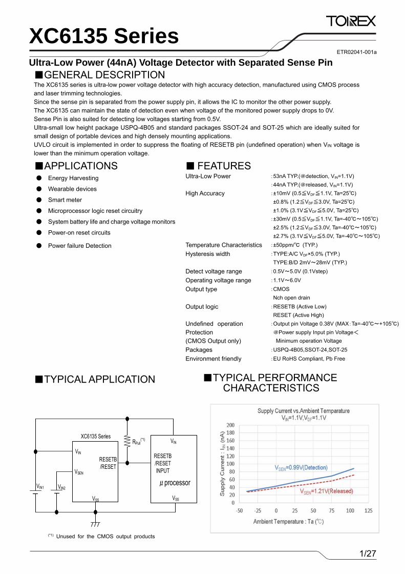
BLOCK DIAGRAMS (1) XC6135C Series A/B type (RESETB OUTPUT: CMOS output/Active Low)
* Diodes inside the circuits are ESD protection diodes and parasitic diodes.
(2) XC6135C Series C/D type (RESETB OUTPUT: CMOS output/Active High)
* Diodes inside the circuits are ESD protection diodes and parasitic diodes.
VSS
VIN
+
- RESETB
VSEN
RSEN=RA+RB+RC
RA
RB
RC
VREF
UVLO
M1
M2
VSS
VIN
+
- RESET
VSEN
RSEN=RA+RB+RC
RA
RB
RC
VREF
UVLO
M1
M2
3/27
XC6135Series
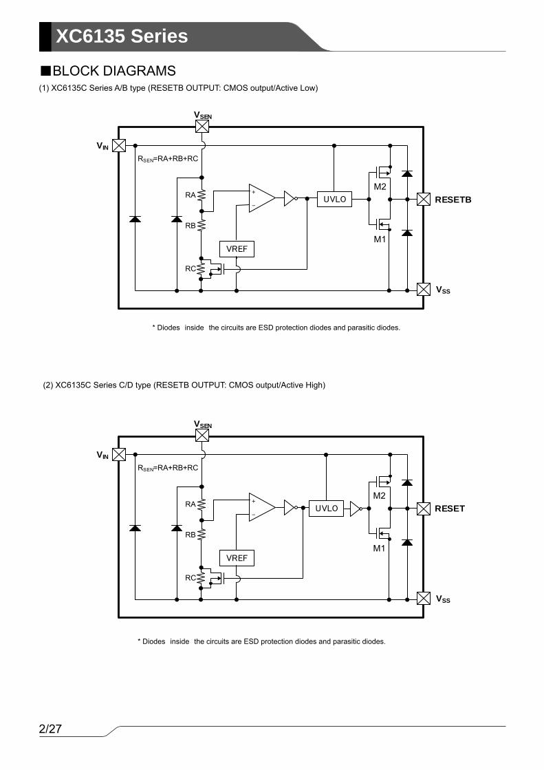
BLOCK DIAGRAMS (3) XC6135N Series A/B type(RESETB OUTPUT: Nch open drain output /Active Low)
* Diodes inside the circuits are ESD protection diodes and parasitic diodes.
(4) XC6135N Series C/D type (RESETB OUTPUT: Nch open drain output /Active High)
* Diodes inside the circuits are ESD protection diodes and parasitic diodes.
VSS
VIN
+
- RESETB
VSEN
RSEN=RA+RB+RC
RA
RB
RC
VREF
UVLO
M1
VSS
VIN
+
- RESET
VSEN
RSEN=RA+RB+RC
RA
RB
RC
VREF
UVLO
M1
4/27
XC6135 Series
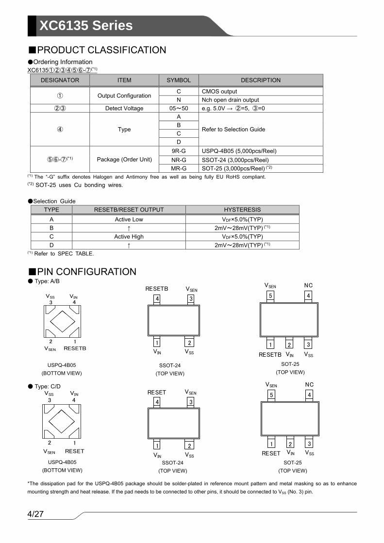
PRODUCT CLASSIFICATION Ordering Information
XC6135①②③④⑤⑥-⑦(*1)
DESIGNATOR ITEM SYMBOL DESCRIPTION
① Output Configuration C CMOS output N Nch open drain output
②③ Detect Voltage 05~50 e.g. 5.0V → ②=5, ③=0
④ Type
A
Refer to Selection Guide B C D
⑤⑥-⑦(*1) Package (Order Unit) 9R-G USPQ-4B05 (5,000pcs/Reel) NR-G SSOT-24 (3,000pcs/Reel) MR-G SOT-25 (3,000pcs/Reel) (*2)
(*1) The “-G” suffix denotes Halogen and Antimony free as well as being fully EU RoHS compliant. (*2) SOT-25 uses Cu bonding wires. Selection Guide
TYPE RESETB/RESET OUTPUT HYSTERESIS
A Active Low VDF×5.0%(TYP) B ↑ 2mV~28mV(TYP) (*1) C Active High VDF×5.0%(TYP) D ↑ 2mV~28mV(TYP) (*1)
(*1) Refer to SPEC TABLE.
PIN CONFIGURATION Type: A/B Type: C/D *The dissipation pad for the USPQ-4B05 package should be solder-plated in reference mount pattern and metal masking so as to enhance mounting strength and heat release. If the pad needs to be connected to other pins, it should be connected to VSS (No. 3) pin.
USPQ-4B05 (BOTTOM VIEW)
SSOT-24 (TOP VIEW)
SOT-25 (TOP VIEW)
USPQ-4B05 (BOTTOM VIEW)
SSOT-24 (TOP VIEW)
SOT-25 (TOP VIEW)
VINVSS
2
3
1
4
VSEN RESETB
RESETB
1 2
34
VIN VSS
VSEN
1 3
45
2
VSSRESETB VIN
NCVSEN
VINVSS
2
3
1
4
RESET VSEN
1 2
34
VSSVIN
RESET VSEN
1 3
45
2
VSSRESET VIN
NCVSEN
5/27
XC6135Series
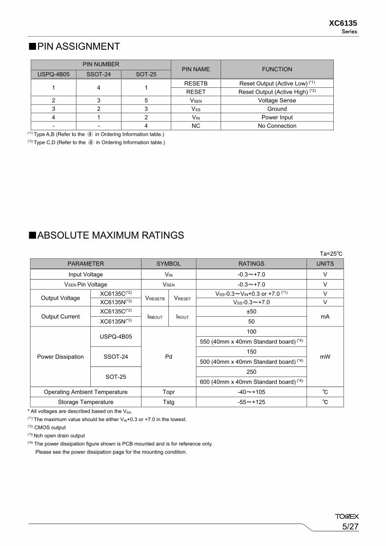
PIN ASSIGNMENT
PIN NUMBER PIN NAME FUNCTION
USPQ-4B05 SSOT-24 SOT-25
1 4 1 RESETB Reset Output (Active Low) (*1) RESET Reset Output (Active High) (*2)
2 3 5 VSEN Voltage Sense 3 2 3 VSS Ground 4 1 2 VIN Power Input - - 4 NC No Connection
(*1) Type A,B (Refer to the ④ in Ordering Information table.) (*2) Type C,D (Refer to the ④ in Ordering Information table.)
ABSOLUTE MAXIMUM RATINGS
Ta=25
PARAMETER SYMBOL RATINGS UNITS
Input Voltage VIN -0.3~+7.0 V
VSEN Pin Voltage VSEN -0.3~+7.0 V
Output Voltage XC6135C(*2)
VRESETB VRESETVSS-0.3~VIN+0.3 or +7.0 (*1) V
XC6135N(*3) VSS-0.3~+7.0 V
Output Current XC6135C(*2)
IRBOUT IROUT ±50
mA XC6135N(*3) 50
Power Dissipation
USPQ-4B05
Pd
100
mW
550 (40mm x 40mm Standard board) (*4)
SSOT-24 150
500 (40mm x 40mm Standard board) (*4)
SOT-25 250
600 (40mm x 40mm Standard board) (*4)
Operating Ambient Temperature Topr -40~+105
Storage Temperature Tstg -55~+125 * All voltages are described based on the VSS. (*1) The maximum value should be either VIN+0.3 or +7.0 in the lowest. (*2) CMOS output (*3) Nch open drain output (*4) The power dissipation figure shown is PCB mounted and is for reference only. Please see the power dissipation page for the mounting condition.
6/27
XC6135 Series
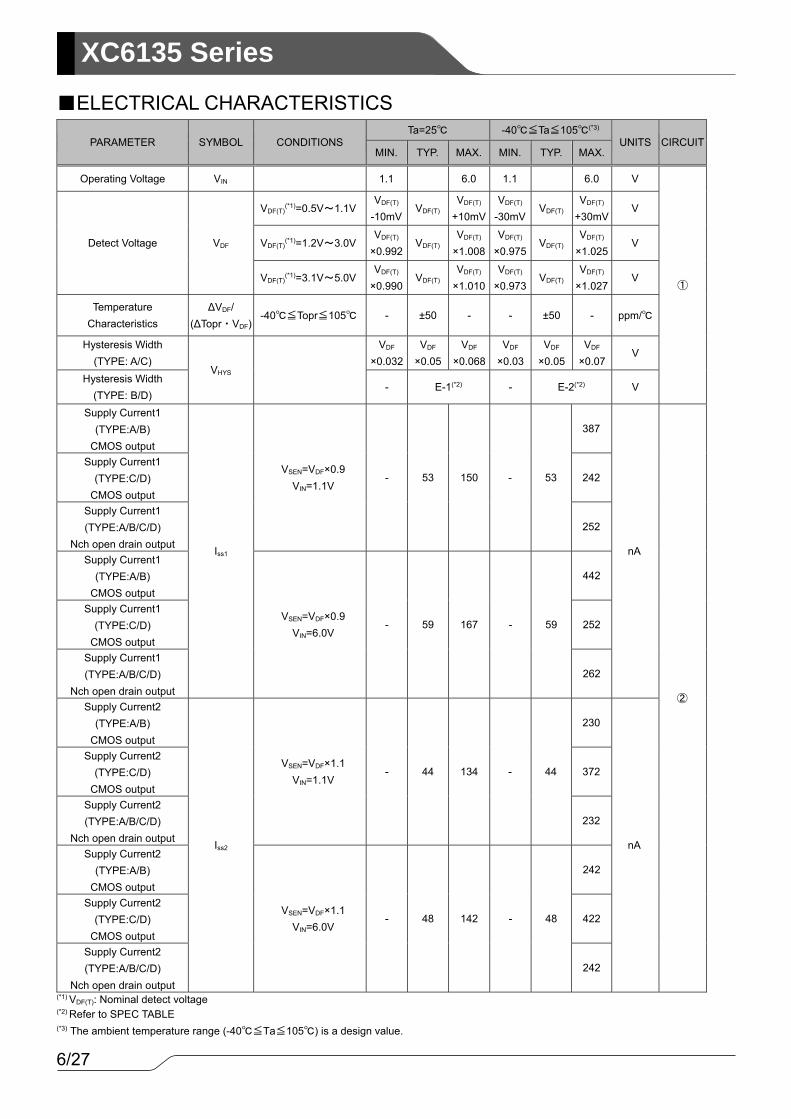
ELECTRICAL CHARACTERISTICS
PARAMETER SYMBOL CONDITIONS Ta=25 -40≦Ta≦105(*3)
UNITS CIRCUITMIN. TYP. MAX. MIN. TYP. MAX.
Operating Voltage VIN 1.1 6.0 1.1 6.0 V
①
Detect Voltage VDF
VDF(T)(*1)=0.5V~1.1V
VDF(T)
-10mVVDF(T)
VDF(T)
+10mVVDF(T)
-30mVVDF(T)
VDF(T) +30mV
V
VDF(T)(*1)=1.2V~3.0V
VDF(T)
×0.992VDF(T)
VDF(T)
×1.008VDF(T)
×0.975VDF(T)
VDF(T) ×1.025
V
VDF(T)(*1)=3.1V~5.0V
VDF(T)
×0.990VDF(T)
VDF(T)
×1.010VDF(T)
×0.973VDF(T)
VDF(T) ×1.027
V
Temperature Characteristics
∆VDF/ (∆Topr・VDF)
-40≦Topr≦105 - ±50 - - ±50 - ppm/
Hysteresis Width (TYPE: A/C)
VHYS
VDF
×0.032VDF
×0.05VDF
×0.068VDF
×0.03VDF
×0.05 VDF
×0.07 V
Hysteresis Width (TYPE: B/D)
- E-1(*2) - E-2(*2) V
Supply Current1 (TYPE:A/B)
CMOS output
Iss1
VSEN=VDF×0.9 VIN=1.1V
- 53 150 - 53
387
nA
②
Supply Current1 (TYPE:C/D)
CMOS output 242
Supply Current1 (TYPE:A/B/C/D)
Nch open drain output 252
Supply Current1 (TYPE:A/B)
CMOS output
VSEN=VDF×0.9 VIN=6.0V
- 59 167 - 59
442
Supply Current1 (TYPE:C/D)
CMOS output 252
Supply Current1 (TYPE:A/B/C/D)
Nch open drain output 262
Supply Current2 (TYPE:A/B)
CMOS output
Iss2
VSEN=VDF×1.1 VIN=1.1V
- 44 134 - 44
230
nA
Supply Current2 (TYPE:C/D)
CMOS output 372
Supply Current2 (TYPE:A/B/C/D)
Nch open drain output 232
Supply Current2 (TYPE:A/B)
CMOS output
VSEN=VDF×1.1 VIN=6.0V
- 48 142 - 48
242
Supply Current2 (TYPE:C/D)
CMOS output 422
Supply Current2 (TYPE:A/B/C/D)
Nch open drain output 242
(*1) VDF(T): Nominal detect voltage (*2) Refer to SPEC TABLE (*3) The ambient temperature range (-40≦Ta≦105) is a design value.
7/27
XC6135Series
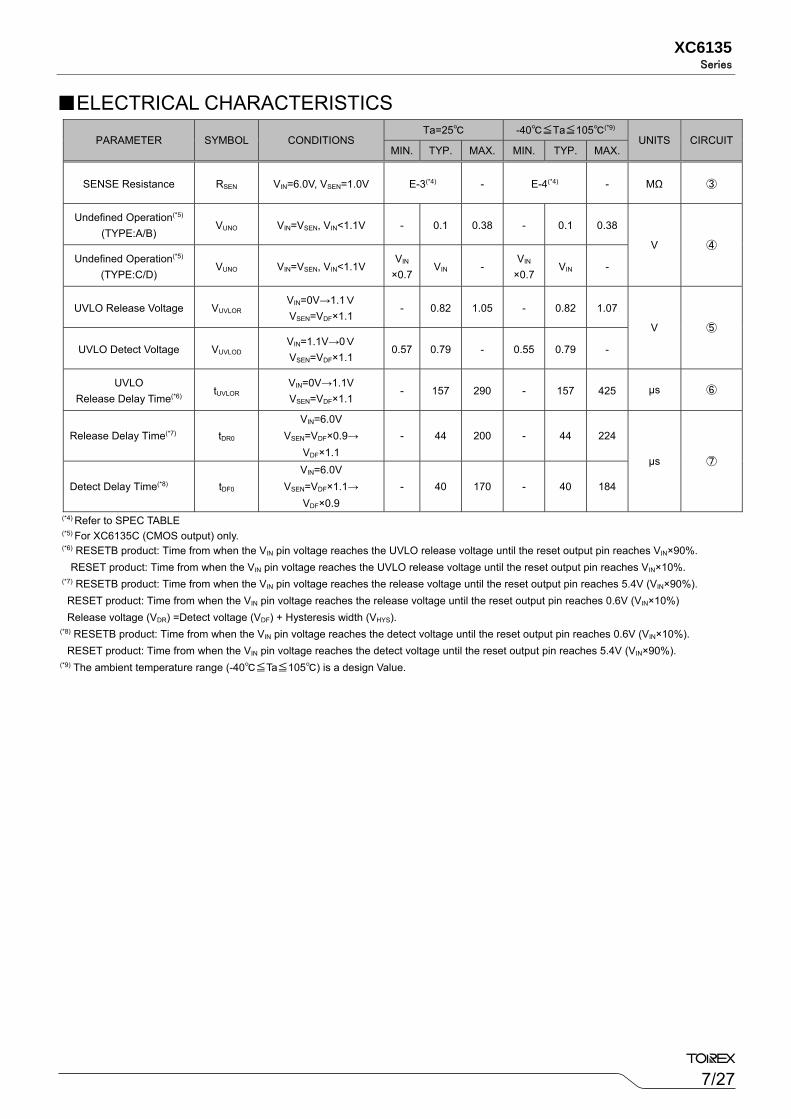
ELECTRICAL CHARACTERISTICS
PARAMETER SYMBOL CONDITIONS Ta=25 -40≦Ta≦105(*9)
UNITS CIRCUITMIN. TYP. MAX. MIN. TYP. MAX.
SENSE Resistance RSEN VIN=6.0V, VSEN=1.0V E-3(*4) - E-4(*4) - MΩ ③
Undefined Operation(*5) (TYPE:A/B)
VUNO VIN=VSEN, VIN<1.1V - 0.1 0.38 - 0.1 0.38
V ④ Undefined Operation(*5)
(TYPE:C/D) VUNO VIN=VSEN, VIN<1.1V
VIN
×0.7VIN -
VIN
×0.7VIN -
UVLO Release Voltage VUVLOR VIN=0V→1.1V VSEN=VDF×1.1
- 0.82 1.05 - 0.82 1.07
V ⑤
UVLO Detect Voltage VUVLOD VIN=1.1V→0V VSEN=VDF×1.1
0.57 0.79 - 0.55 0.79 -
UVLO Release Delay Time(*6)
tUVLOR VIN=0V→1.1V VSEN=VDF×1.1
- 157 290 - 157 425 µs ⑥
Release Delay Time(*7) tDR0 VIN=6.0V
VSEN=VDF×0.9→ VDF×1.1
- 44 200 - 44 224
µs ⑦
Detect Delay Time(*8) tDF0 VIN=6.0V
VSEN=VDF×1.1→ VDF×0.9
- 40 170 - 40 184
(*4) Refer to SPEC TABLE
(*5) For XC6135C (CMOS output) only. (*6) RESETB product: Time from when the VIN pin voltage reaches the UVLO release voltage until the reset output pin reaches VIN×90%.
RESET product: Time from when the VIN pin voltage reaches the UVLO release voltage until the reset output pin reaches VIN×10%. (*7) RESETB product: Time from when the VIN pin voltage reaches the release voltage until the reset output pin reaches 5.4V (VIN×90%). RESET product: Time from when the VIN pin voltage reaches the release voltage until the reset output pin reaches 0.6V (VIN×10%) Release voltage (VDR) =Detect voltage (VDF) + Hysteresis width (VHYS).
(*8) RESETB product: Time from when the VIN pin voltage reaches the detect voltage until the reset output pin reaches 0.6V (VIN×10%). RESET product: Time from when the VIN pin voltage reaches the detect voltage until the reset output pin reaches 5.4V (VIN×90%).
(*9) The ambient temperature range (-40≦Ta≦105) is a design Value.
8/27
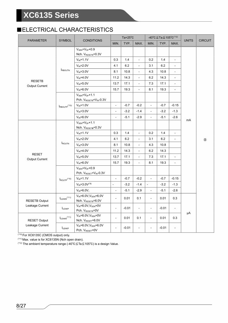
XC6135 Series
ELECTRICAL CHARACTERISTICS
PARAMETER SYMBOL CONDITIONS Ta=25 -40≦Ta≦105(*12)
UNITS CIRCUITMIN. TYP. MAX. MIN. TYP. MAX.
RESETB Output Current
IRBOUTN
VSEN=VDF×0.9 Nch. VRESETB=0.3V
mA
⑧
VIN=1.1V 0.3 1.4 - 0.2 1.4 -
VIN=2.0V 4.1 6.2 - 3.1 6.2 -
VIN=3.0V 8.1 10.8 - 4.3 10.8 -
VIN=4.0V 11.2 14.3 - 6.2 14.3 -
VIN=5.0V 13.7 17.1 - 7.3 17.1 -
VIN=6.0V 15.7 19.3 - 8.1 19.3 -
IRBOUTP(*10)
VSEN=VDF×1.1 Pch. VRESETB=VIN-0.3V
VIN=1.0V - -0.7 -0.2 - -0.7 -0.15
VIN=3.0V - -3.2 -1.4 - -3.2 -1.3
VIN=6.0V - -5.1 -2.9 - -5.1 -2.6
RESET Output Current
IROUTN
VSEN=VDF×1.1 Nch. VRESETB=0.3V
VIN=1.1V 0.3 1.4 - 0.2 1.4 -
VIN=2.0V 4.1 6.2 - 3.1 6.2 -
VIN=3.0V 8.1 10.8 - 4.3 10.8
VIN=4.0V 11.2 14.3 - 6.2 14.3
VIN=5.0V 13.7 17.1 - 7.3 17.1 -
VIN=6.0V 15.7 19.3 - 8.1 19.3 -
IROUTP(*10)
VSEN=VDF×0.9 Pch. VRESET=VIN-0.3V
VIN=1.1V - -0.7 -0.2 - -0.7 -0.15
VIN=3.0V(*8) - -3.2 -1.4 - -3.2 -1.3
VIN=6.0V, - -5.1 -2.9 - -5.1 -2.6
RESETB Output
Leakage Current
ILEAKN(*11)
VIN=6.0V,VSEN=6.0V Nch. VRESETB=6.0V
- 0.01 0.1 - 0.01 0.3
µA ILEAKP
VIN=6.0V,VSEN=0V Pch. VRESETB=0V
- -0.01 - - -0.01 -
RESET Output
Leakage Current
ILEAKN(*11)
VIN=6.0V,VSEN=0V
Nch. VRESET=6.0V - 0.01 0.1 - 0.01 0.3
ILEAKP VIN=6.0V,VSEN=6.0V
Pch. VRESET=0V - -0.01 - - -0.01 -
(*10) For XC6135C (CMOS output) only.
(*11) Max. value is for XC6135N (Nch open drain).
(*12) The ambient temperature range (-40≦Ta≦105) is a design Value.
9/27
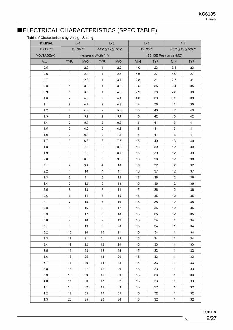
XC6135Series
ELECTRICAL CHARACTERISTICS (SPEC TABLE) Table of Characteristics by Voltage Setting
NOMINAL E-1 E-2 E-3 E-4
DETECT Ta=25 -40≦Ta≦105 Ta=25 -40≦Ta≦105
VOLTAGE(V) Hysteresis Width (mV) SENSE Resistance (MΩ)
VDF(T) TYP. MAX. TYP. MAX. MIN TYP. MIN TYP.
0.5 1 2.0 1 2.2 4.0 23 3.1 23
0.6 1 2.4 1 2.7 3.6 27 3.0 27
0.7 1 2.8 1 3.1 2.8 31 2.7 31
0.8 1 3.2 1 3.5 2.5 35 2.4 35
0.9 1 3.6 1 4.0 2.9 38 2.8 38
1.0 2 4.0 2 4.4 4.0 39 3.9 39
1.1 2 4.4 2 4.9 14 39 11 39
1.2 2 4.8 2 5.3 15 40 12 40
1.3 2 5.2 2 5.7 16 42 13 42
1.4 2 5.6 2 6.2 17 41 13 41
1.5 2 6.0 2 6.6 16 41 13 41
1.6 2 6.4 2 7.1 16 41 13 41
1.7 3 6.8 3 7.5 16 40 13 40
1.8 3 7.2 3 8.0 16 39 12 39
1.9 3 7.9 3 8.7 16 39 12 39
2.0 3 8.6 3 9.5 16 38 12 38
2.1 4 9.4 4 10 16 37 12 37
2.2 4 10 4 11 16 37 12 37
2.3 5 11 5 12 16 36 12 36
2.4 5 12 5 13 15 36 12 36
2.5 6 13 6 14 15 36 12 36
2.6 6 14 6 15 15 35 12 35
2.7 7 15 7 16 15 35 12 35
2.8 8 16 8 17 15 35 12 35
2.9 8 17 8 18 15 35 12 35
3.0 9 18 9 19 15 34 11 34
3.1 9 19 9 20 15 34 11 34
3.2 10 20 10 21 15 34 11 34
3.3 11 21 11 23 15 34 11 34
3.4 12 22 12 24 15 33 11 33
3.5 12 23 12 25 15 33 11 33
3.6 13 25 13 26 15 33 11 33
3.7 14 26 14 28 15 33 11 33
3.8 15 27 15 29 15 33 11 33
3.9 16 29 16 30 15 33 11 33
4.0 17 30 17 32 15 33 11 33
4.1 18 32 18 33 15 32 11 32
4.2 19 33 19 35 15 32 11 32
4.3 20 35 20 36 15 32 11 32
10/27
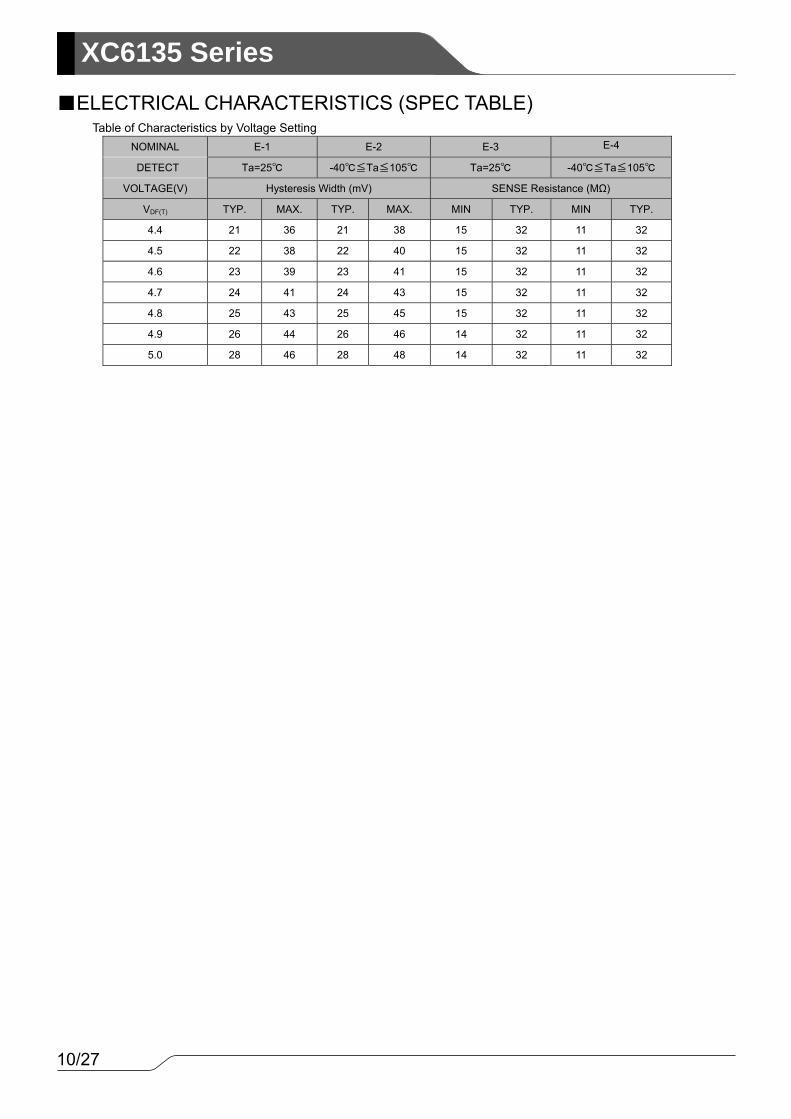
XC6135 Series
ELECTRICAL CHARACTERISTICS (SPEC TABLE) Table of Characteristics by Voltage Setting
NOMINAL E-1 E-2 E-3 E-4
DETECT Ta=25 -40≦Ta≦105 Ta=25 -40≦Ta≦105
VOLTAGE(V) Hysteresis Width (mV) SENSE Resistance (MΩ)
VDF(T) TYP. MAX. TYP. MAX. MIN TYP. MIN TYP.
4.4 21 36 21 38 15 32 11 32
4.5 22 38 22 40 15 32 11 32
4.6 23 39 23 41 15 32 11 32
4.7 24 41 24 43 15 32 11 32
4.8 25 43 25 45 15 32 11 32
4.9 26 44 26 46 14 32 11 32
5.0 28 46 28 48 14 32 11 32
11/27
XC6135Series
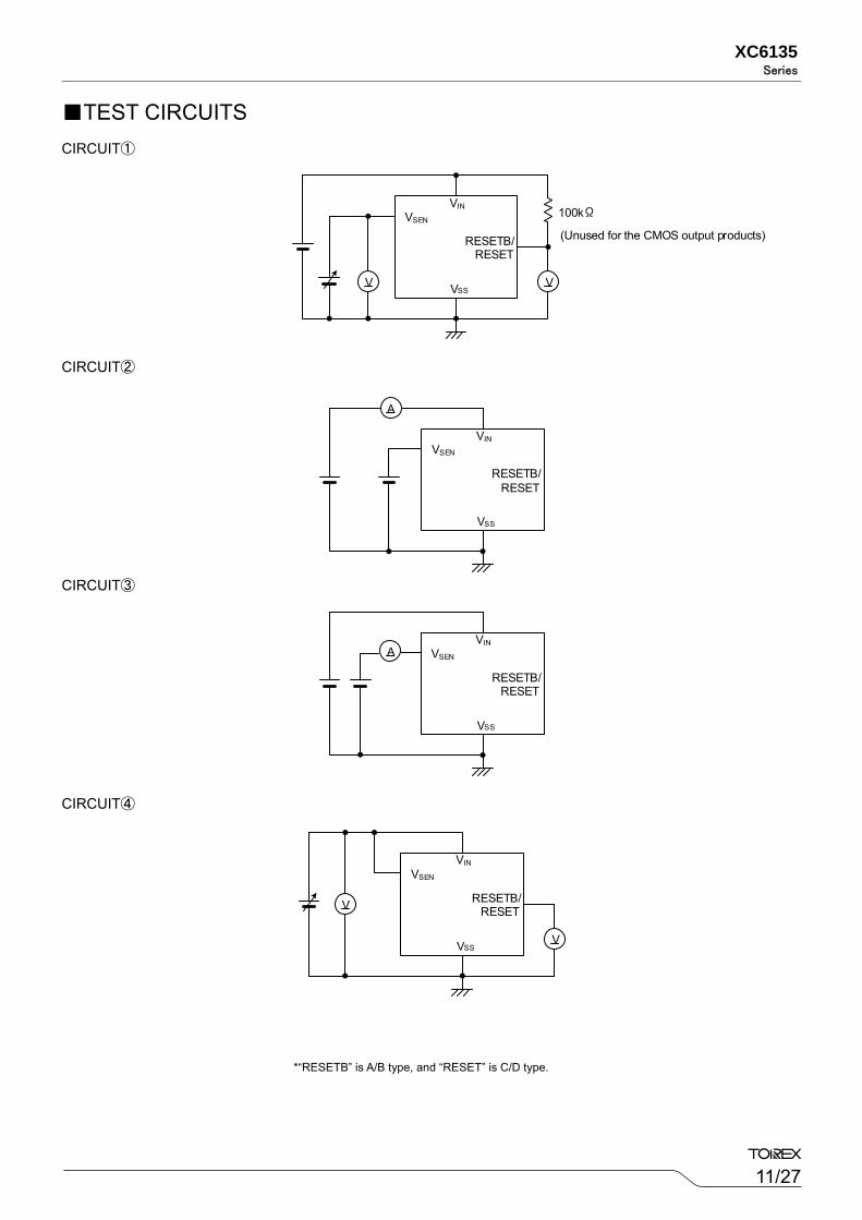
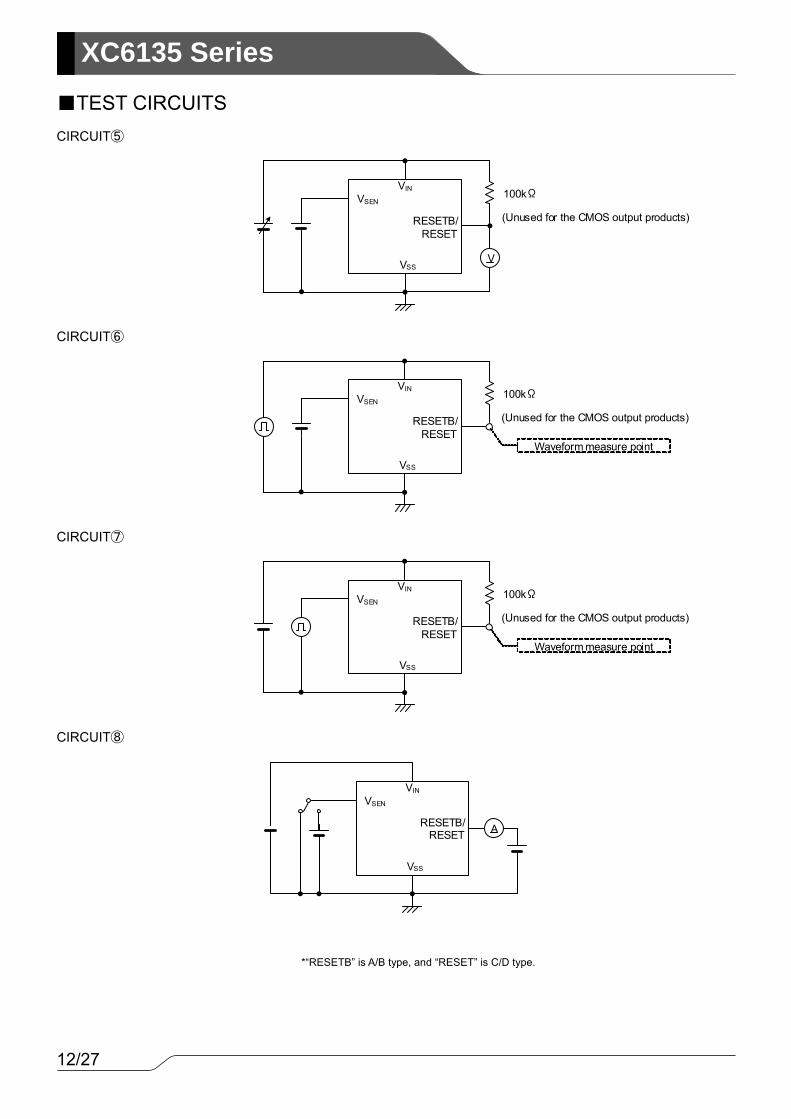
TEST CIRCUITS
CIRCUIT①
CIRCUIT②
CIRCUIT③
CIRCUIT④
*“RESETB” is A/B type, and “RESET” is C/D type.
100kΩVSEN
RESETB/RESET
VSSV V
(Unused for the CMOS output products)
VIN
A
VSEN
VSS
RESETB/RESET
VIN
VSEN
VSS
RESETB/RESET
AVIN
VSEN
RESETB/RESET
VSSV
V
VIN
12/27
XC6135 Series
TEST CIRCUITS CIRCUIT⑤
CIRCUIT⑥
CIRCUIT⑦
CIRCUIT⑧
*“RESETB” is A/B type, and “RESET” is C/D type.
VSEN
RESETB/RESET
VSS
(Unused for the CMOS output products)
100kΩVIN
V
VSEN
RESETB/RESET
VSS
Waveform measure point
(Unused for the CMOS output products)
100kΩVIN
VSEN
RESETB/RESET
VSS
Waveform measure point
(Unused for the CMOS output products)
100kΩVIN
VSEN
VSS
RESETB/RESET A
VIN
13/27
XC6135Series
SENSE Voltage : VSEN
Release Voltage : VDR=VDF+VHYS
Detect Voltage : VDF
Output Voltage : VRESETB
① ② ③ ④
Ground Voltage : VSS
Ground Voltage : VSS
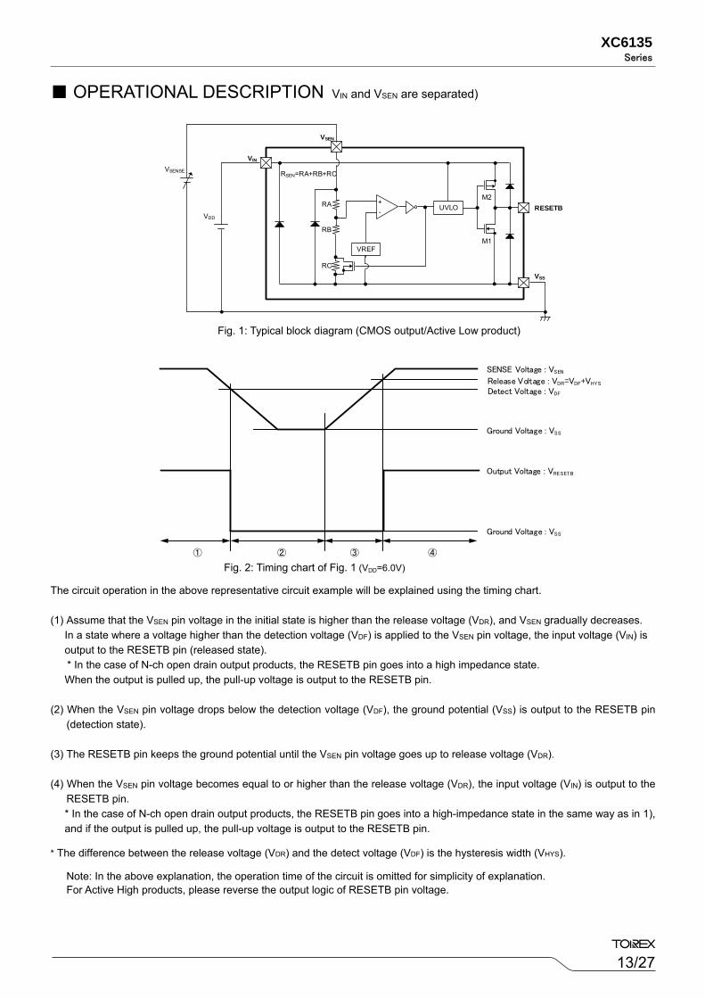
OPERATIONAL DESCRIPTION VIN and VSEN are separated) The circuit operation in the above representative circuit example will be explained using the timing chart. (1) Assume that the VSEN pin voltage in the initial state is higher than the release voltage (VDR), and VSEN gradually decreases.
In a state where a voltage higher than the detection voltage (VDF) is applied to the VSEN pin voltage, the input voltage (VIN) is output to the RESETB pin (released state).
* In the case of N-ch open drain output products, the RESETB pin goes into a high impedance state. When the output is pulled up, the pull-up voltage is output to the RESETB pin.
(2) When the VSEN pin voltage drops below the detection voltage (VDF), the ground potential (VSS) is output to the RESETB pin (detection state).
(3) The RESETB pin keeps the ground potential until the VSEN pin voltage goes up to release voltage (VDR). (4) When the VSEN pin voltage becomes equal to or higher than the release voltage (VDR), the input voltage (VIN) is output to the
RESETB pin. * In the case of N-ch open drain output products, the RESETB pin goes into a high-impedance state in the same way as in 1), and if the output is pulled up, the pull-up voltage is output to the RESETB pin.
* The difference between the release voltage (VDR) and the detect voltage (VDF) is the hysteresis width (VHYS).
Note: In the above explanation, the operation time of the circuit is omitted for simplicity of explanation. For Active High products, please reverse the output logic of RESETB pin voltage.
Fig. 2: Timing chart of Fig. 1 (VDD=6.0V)
Fig. 1: Typical block diagram (CMOS output/Active Low product)
VIN
+- RESETB
VSEN
RSEN=RA+RB+RC
RA
RB
RC
VREF
UVLO
M1
M2
VDD
VSS
VSENSE
14/27
XC6135 Series
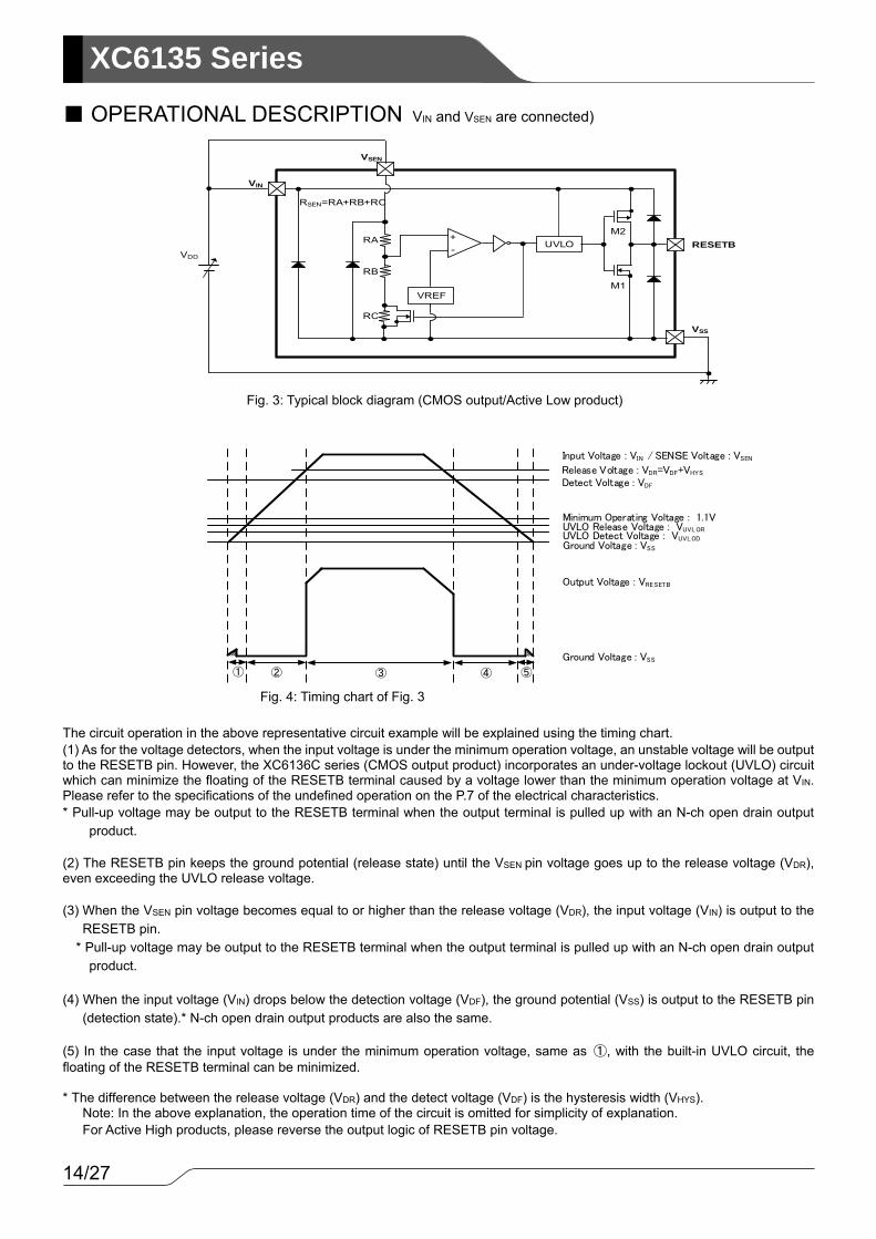
OPERATIONAL DESCRIPTION VIN and VSEN are connected) The circuit operation in the above representative circuit example will be explained using the timing chart. (1) As for the voltage detectors, when the input voltage is under the minimum operation voltage, an unstable voltage will be output to the RESETB pin. However, the XC6136C series (CMOS output product) incorporates an under-voltage lockout (UVLO) circuit which can minimize the floating of the RESETB terminal caused by a voltage lower than the minimum operation voltage at VIN. Please refer to the specifications of the undefined operation on the P.7 of the electrical characteristics. * Pull-up voltage may be output to the RESETB terminal when the output terminal is pulled up with an N-ch open drain output
product. (2) The RESETB pin keeps the ground potential (release state) until the VSEN pin voltage goes up to the release voltage (VDR), even exceeding the UVLO release voltage. (3) When the VSEN pin voltage becomes equal to or higher than the release voltage (VDR), the input voltage (VIN) is output to the
RESETB pin. * Pull-up voltage may be output to the RESETB terminal when the output terminal is pulled up with an N-ch open drain output
product. (4) When the input voltage (VIN) drops below the detection voltage (VDF), the ground potential (VSS) is output to the RESETB pin
(detection state).* N-ch open drain output products are also the same. (5) In the case that the input voltage is under the minimum operation voltage, same as ①, with the built-in UVLO circuit, the floating of the RESETB terminal can be minimized. * The difference between the release voltage (VDR) and the detect voltage (VDF) is the hysteresis width (VHYS).
Note: In the above explanation, the operation time of the circuit is omitted for simplicity of explanation. For Active High products, please reverse the output logic of RESETB pin voltage.
Fig. 4: Timing chart of Fig. 3
Fig. 3: Typical block diagram (CMOS output/Active Low product)
VIN
+- RESETB
VSEN
RSEN=RA+RB+RC
RA
RB
RC
VREF
UVLO
M1
M2
VDD
VSS
Input Voltage : VIN / SENSE Voltage : VSEN Release Voltage : VDR=VDF+VHYS
Detect Voltage : VDF
UVLO Release Voltage : VUVLOR
Output Voltage : VRESETB
Ground Voltage : VSS
Ground Voltage : VSS
Minimum Operating Voltage : 1.1V
UVLO Detect Voltage : VUVLOD
① ⑤② ④③
15/27
XC6135Series
NOTES ON USE (1) Please use this IC within the stated maximum ratings. For temporary, transitional voltage drop or voltage rising phenomenon,
the IC is liable to malfunction should the ratings be exceeded.
(2) The power input pin voltage may fall due to the flow through current during IC operation and the resistance component between the power supply and the power input pin. In the case of CMOS output, a drop in the power input pin voltage may occur in the same way due to the output current. When this happens, if the power input pin voltage drops below the minimum operating voltage, a malfunction may occur.
(3) Note that large, sharp changes of the power input pin voltage may lead to malfunction. (4) Since the power supply noise may cause malfunction, please fully evaluate with an actual system. As necessary, please take
measures such as inserting a capacitor between VIN and VSS. (5) When an N-ch open drain output is used, the VRESETB voltage at detection and release is determined by the pull-up resistance
connected to the output pin. Refer to the following when selecting the resistance value. At detection:
VRESETB = Vpull / (1 + Rpull / RON) Vpull :Voltage after pull-up
RON(*1) :ON resistance of N-ch driver M1 (calculated from VRESETB/IRBOUTN based on electrical characteristics)
Example: When VIN=2.0V(*2), RON = 0.3V / (4.1 × 10⁻³ A) ≒ 73.2Ω (MAX.) If it is desired to make VRESETB at detection 0.1V or less when Vpull is 3.0V, Rpull = ( Vpull / VRESETB ) – 1 × RON = ( 3V / 0.1V ) – 1 × 73.2Ω ≒ 2.1kΩ
Therefore, to make the output voltage at detection 0.1V or less under the above conditions, the pull-up resistance must be 2.1kΩ or higher. (*1) Note that RON becomes larger as VIN becomes smaller. (*2) For VIN in the calculation, use the lowest value of the input voltage range you will use.
At release: VRESETB = Vpull / ( 1 + Rpull / Roff )
Vpull :Voltage after pull-up Roff :Resistance when N-ch driver M1 is OFF (calculated from VRESETB/ILEAKN based on electrical characteristics)
Example: When Vpull is 6.0V, Roff = 6V / ( 0.1 × 10⁻⁶ A) = 60MΩ (MIN.).
If it is desired to make VRESETB 5.99V or higher, Rpull = ( Vpull / VRESETB ) – 1 × Roff = ( 6V / 5.99V ) – 1 × 60 × 106Ω ≒ 100kΩ
Therefore, to make the output voltage at release 5.99V or higher under the above conditions, the pull-up resistance must be 100kΩ or less.The above VRESETB voltage is an example calculation of Active Low products. To calculate the VRESET voltage (Active High product), calculate by inverting the logic at detection and release.
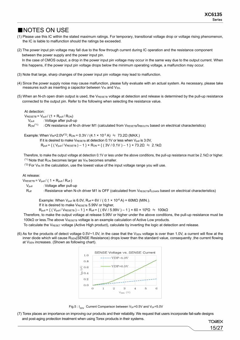
(6) As for the products of detect voltage 0.5V~1.0V, in the case that the VSEN voltage is over than 1.0V, a current will flow at the
inner diode which will cause RSEN(SENSE Resistance) drops lower than the standard value, consequently ,the current flowing at VSEN increases. (Shown as following chart).
(7) Torex places an importance on improving our products and their reliability. We request that users incorporate fail-safe designs
and post-aging protection treatment when using Torex products in their systems.
Fig.5 : ISEN Current Comparison between VDF=0.5V and VDF=5.0V
16/27
XC6135 Series
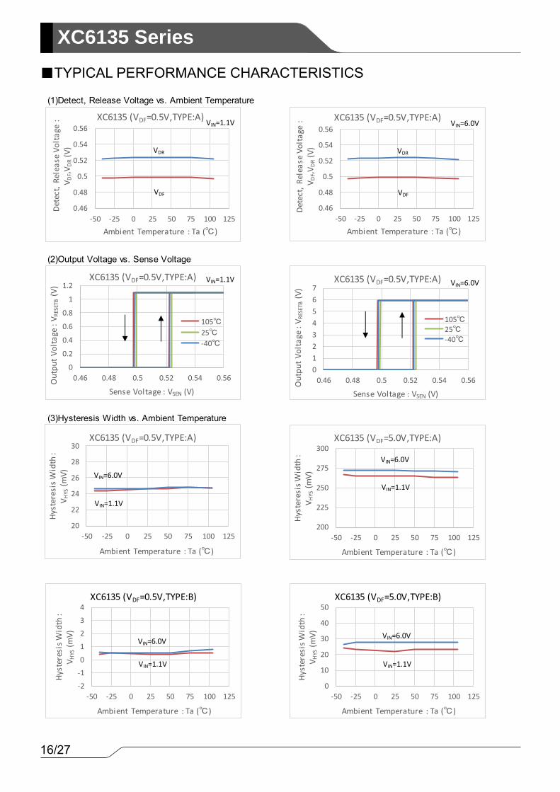
TYPICAL PERFORMANCE CHARACTERISTICS
(1)Detect, Release Voltage vs. Ambient Temperature
(2)Output Voltage vs. Sense Voltage
(3)Hysteresis Width vs. Ambient Temperature
0.46
0.48
0.5
0.52
0.54
0.56
‐50 ‐25 0 25 50 75 100 125
Detect, R
elease Voltage :
V DF,V
DR(V)
Ambient Temperature : Ta ()
XC6135 (VDF=0.5V,TYPE:A) VIN=1.1V
VDF
VDR
0.46
0.48
0.5
0.52
0.54
0.56
‐50 ‐25 0 25 50 75 100 125
Detect, R
elease Voltage :
V DF,V
DR(V)
Ambient Temperature : Ta ()
XC6135 (VDF=0.5V,TYPE:A) VIN=6.0V
VDF
VDR
01234567
0.46 0.48 0.5 0.52 0.54 0.56Outpu
t Voltage : V R
ESETB(V)
Sense Voltage : VSEN (V)
XC6135 (VDF=0.5V,TYPE:A)
10525‐40
VIN=6.0V
0
0.2
0.4
0.6
0.8
1
1.2
0.46 0.48 0.5 0.52 0.54 0.56Outpu
t Voltage : V R
ESETB(V)
Sense Voltage : VSEN (V)
XC6135 (VDF=0.5V,TYPE:A)
10525‐40
VIN=1.1V
200
225
250
275
300
‐50 ‐25 0 25 50 75 100 125
Hysteresis W
idth :
V HYS(m
V)
Ambient Temperature : Ta ()
XC6135 (VDF=5.0V,TYPE:A)
VIN=1.1V
VIN=6.0V
20
22
24
26
28
30
‐50 ‐25 0 25 50 75 100 125
Hysteresis W
idth :
V HYS(m
V)
Ambient Temperature : Ta ()
XC6135 (VDF=0.5V,TYPE:A)
VIN=1.1V
VIN=6.0V
‐2
‐1
0
1
2
3
4
‐50 ‐25 0 25 50 75 100 125
Hysteresis W
idth :
V HYS(m
V)
Ambient Temperature : Ta ()
XC6135 (VDF=0.5V,TYPE:B)
VIN=1.1V
VIN=6.0V
0
10
20
30
40
50
‐50 ‐25 0 25 50 75 100 125
Hysteresis W
idth :
V HYS(m
V)
Ambient Temperature : Ta ()
XC6135 (VDF=5.0V,TYPE:B)
VIN=1.1V
VIN=6.0V
17/27
XC6135Series
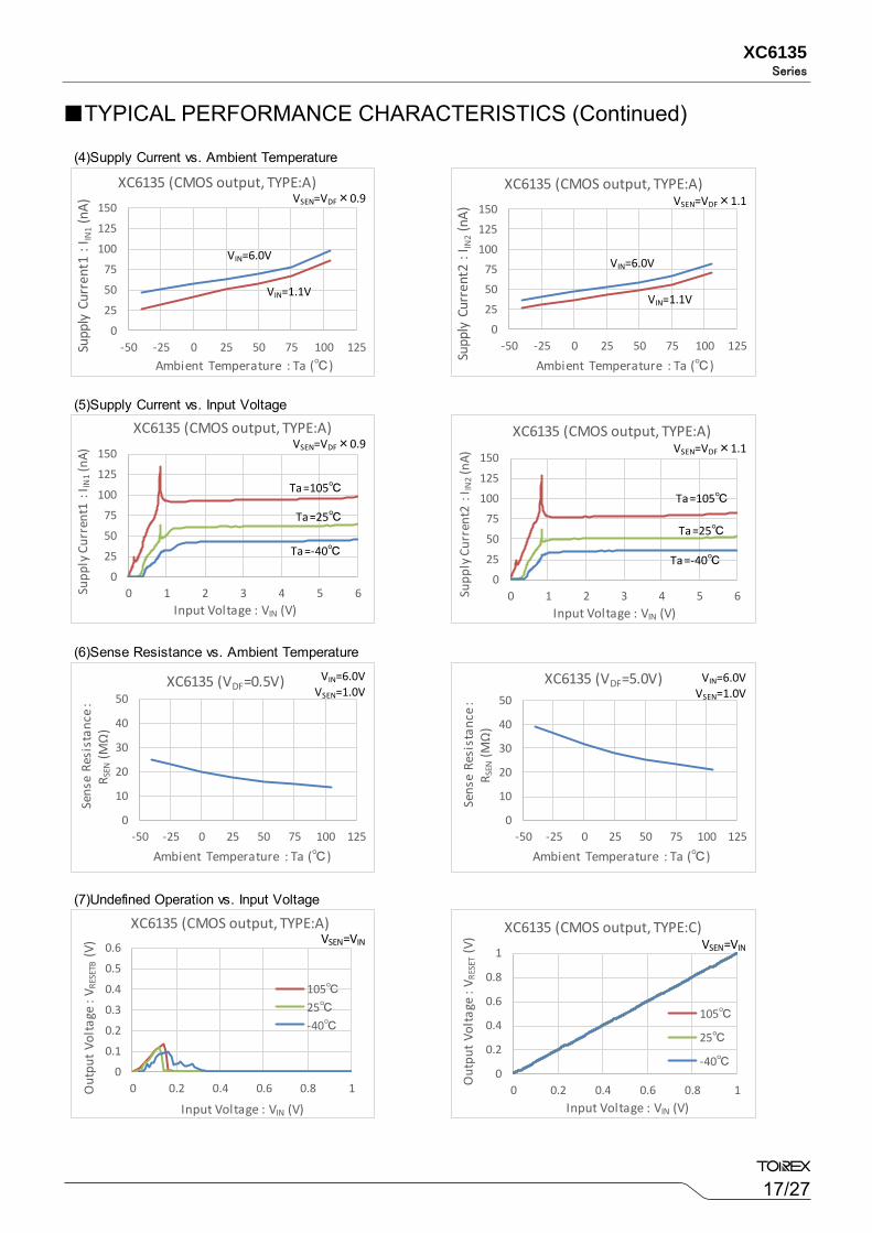
TYPICAL PERFORMANCE CHARACTERISTICS (Continued)
(4)Supply Current vs. Ambient Temperature
(5)Supply Current vs. Input Voltage
(6)Sense Resistance vs. Ambient Temperature
(7)Undefined Operation vs. Input Voltage
0
10
20
30
40
50
‐50 ‐25 0 25 50 75 100 125
Sense Resistan
ce :
R SEN(M
Ω)
Ambient Temperature : Ta ()
XC6135 (VDF=0.5V) VIN=6.0VVSEN=1.0V
0
10
20
30
40
50
‐50 ‐25 0 25 50 75 100 125
Sense Resistan
ce :
R SEN(M
Ω)
Ambient Temperature : Ta ()
XC6135 (VDF=5.0V) VIN=6.0VVSEN=1.0V
0
0.1
0.2
0.3
0.4
0.5
0.6
0 0.2 0.4 0.6 0.8 1Outpu
t Voltage : V R
ESETB(V)
Input Voltage : VIN (V)
XC6135 (CMOS output, TYPE:A)
10525‐40
VSEN=VIN
0
0.2
0.4
0.6
0.8
1
0 0.2 0.4 0.6 0.8 1
Outpu
t Voltage : V R
ESET(V)
Input Voltage : VIN (V)
XC6135 (CMOS output, TYPE:C)
105
25
‐40
VSEN=VIN
0
25
50
75
100
125
150
‐50 ‐25 0 25 50 75 100 125Supply Current1 : I
IN1(nA)
Ambient Temperature : Ta ()
XC6135 (CMOS output, TYPE:A)VSEN=VDF×0.9
VIN=1.1V
VIN=6.0V
0
25
50
75
100
125
150
‐50 ‐25 0 25 50 75 100 125
Supply Current2 : I
IN2(nA)
Ambient Temperature : Ta ()
XC6135 (CMOS output, TYPE:A)VSEN=VDF×1.1
VIN=1.1V
VIN=6.0V
0
25
50
75
100
125
150
0 1 2 3 4 5 6Supp
ly Current1 : I
IN1(nA)
Input Voltage : VIN (V)
XC6135 (CMOS output, TYPE:A)VSEN=VDF×0.9
Ta=‐40
Ta=25
Ta=105
0
25
50
75
100
125
150
0 1 2 3 4 5 6Supp
ly Current2 : I
IN2(nA)
Input Voltage : VIN (V)
XC6135 (CMOS output, TYPE:A)VSEN=VDF×1.1
Ta=‐40
Ta=25
Ta=105
18/27
XC6135 Series
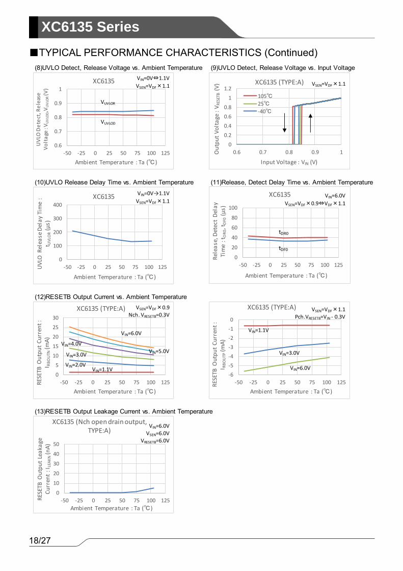
TYPICAL PERFORMANCE CHARACTERISTICS (Continued)
(8)UVLO Detect, Release Voltage vs. Ambient Temperature (9)UVLO Detect, Release Voltage vs. Input Voltage
(10)UVLO Release Delay Time vs. Ambient Temperature (11)Release, Detect Delay Time vs. Ambient Temperature
(12)RESETB Output Current vs. Ambient Temperature
(13)RESETB Output Leakage Current vs. Ambient Temperature
0
100
200
300
400
‐50 ‐25 0 25 50 75 100 125UVLO
Release Delay
Tim
e :
t UVLOR(μs)
Ambient Temperature : Ta ()
XC6135 VIN=0V→1.1VVSEN=VDF×1.1
0
20
40
60
80
100
‐50 ‐25 0 25 50 75 100 125
Release, Detect De
lay
Time : t
DR0, t
DF0(μs)
Ambient Temperature : Ta ()
XC6135
tDR0
VIN=6.0VVSEN=VDF×0.9⇔VDF×1.1
tDF0
0
5
10
15
20
25
30
‐50 ‐25 0 25 50 75 100 125RESETB
Outpu
t Current :
I RBO
UTN(m
A)
Ambient Temperature : Ta ()
XC6135 (TYPE:A) VSEN=VDF×0.9Nch. VRESETB=0.3V
VIN=6.0V
VIN=5.0VVIN=4.0V
VIN=3.0V
VIN=2.0V VIN=1.1V‐6‐5‐4
‐3‐2‐10
‐50 ‐25 0 25 50 75 100 125RESETB
Outpu
t Current :
I RBO
UTP(m
A)
Ambient Temperature : Ta ()
XC6135 (TYPE:A) VSEN=VDF×1.1Pch.VRESETB=VIN ‐ 0.3V
VIN=1.1V
VIN=6.0V
VIN=3.0V
0
10
20
30
40
50
‐50 ‐25 0 25 50 75 100 125RESETB
Outpu
t Leakage
Current : I L
EAKN(nA)
Ambient Temperature : Ta ()
XC6135 (Nch open drain output, TYPE:A)
VIN=6.0VVSEN=6.0V
VRESETB=6.0V
0.6
0.7
0.8
0.9
1
‐50 ‐25 0 25 50 75 100 125
UVLO Detect, Re
lease
Voltage : V
UVLOD,V U
VLOR(V)
Ambient Temperature : Ta ()
XC6135
VUVLOD
VUVLOR
VIN=0V⇔1.1VVSEN=VDF×1.1
0
0.2
0.4
0.6
0.8
1
1.2
0.6 0.7 0.8 0.9 1Outpu
t Voltage : V R
ESETB(V)
Input Voltage : VIN (V)
XC6135 (TYPE:A)
10525‐40
VSEN=VDF×1.1
19/27
XC6135Series
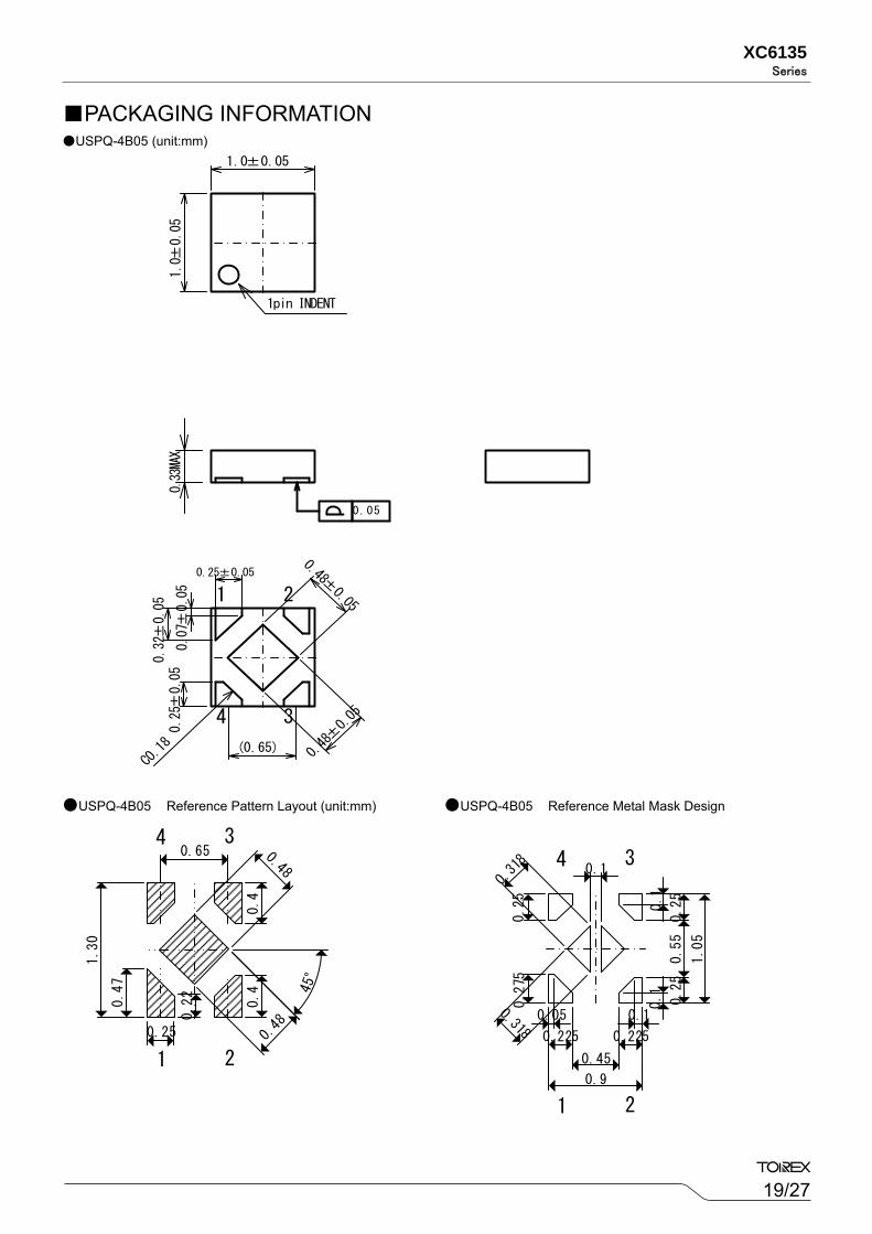
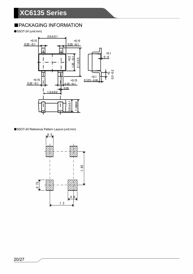
PACKAGING INFORMATION USPQ-4B05 (unit:mm)
1pin INDENT
1 2
34
0.25±0.05
1.0±0.05
0.07±
0.05
0.32±
0.05
(0.65)
0.25±
0.05
1.0±
0.05
0.05
0.33MAX
USPQ-4B05 Reference Pattern Layout (unit:mm) USPQ-4B05 Reference Metal Mask Design
1.30
0.47
0.25
0.22
0.4
0.4
0.65
1 2
34
0.05 0.1
0.1
0.1
0.1
0.275
0.225
0.9
0.45
0.225
0.25
1.05
0.55
0.25
0.25
1 2
34
20/27
XC6135 Series
PACKAGING INFORMATION SSOT-24 (unit:mm)
2.0±0.1
2.1±
0.3
0.9±
0.1
0.125+0.1-0.05
1.3±0.2
0.25+0.15-0.1
1.25
+0.2
-0.1 0
+0.1-0
0.3
+0 -0.2
1.1M
AX
0.35+0.15-0.1
0.05
0.25+0.15-0.1
0.25+0.15-0.1
SSOT-24 Reference Pattern Layout (unit:mm)
0.75
0.5
1.85
1.3
0.6
21/27
XC6135Series
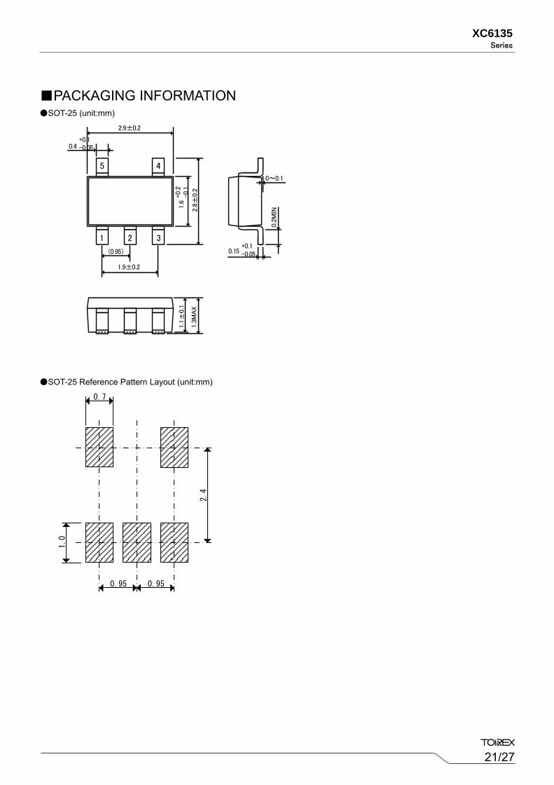
PACKAGING INFORMATION SOT-25 (unit:mm)
1 3
2.9±0.2
0.4+0.1-0.05
1.6
+0.2
-0.1
1.9±0.2
2.8±
0.2
1.1±
0.1
1.3M
AX
0.15+0.1-0.05
0.2M
IN
0~0.1
2
5 4
(0.95)
SOT-25 Reference Pattern Layout (unit:mm)
2.4
1.0
0.7
0.95 0.95
22/27
XC6135 Series
23/27
XC6135Series
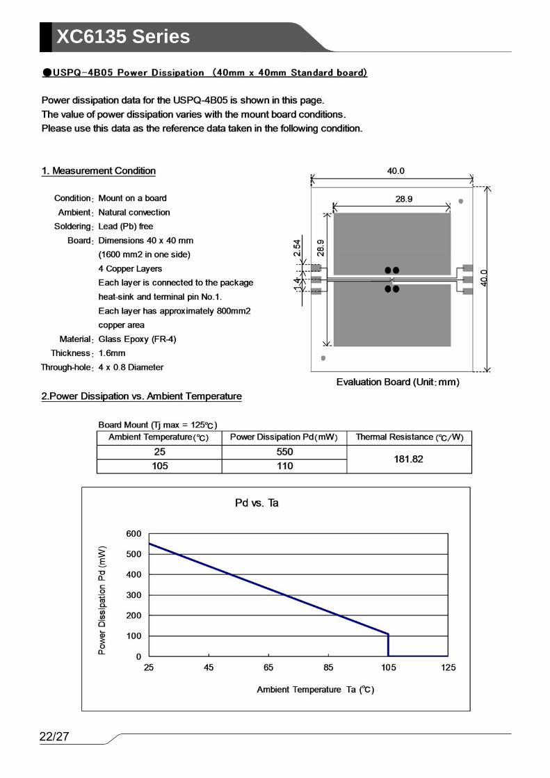
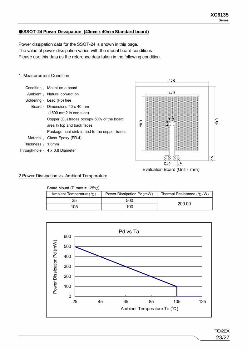
SSOT-24 Power Dissipation (40mm x 40mm Standard board)
Power dissipation data for the SSOT-24 is shown in this page.The value of power dissipation varies with the mount board conditions.Please use this data as the reference data taken in the following condition.
1. Measurement Condition
Condition: Mount on a boardAmbient: Natural convection
Soldering: Lead (Pb) freeBoard: Dimensions 40 x 40 mm
(1600 mm2 in one side) Copper (Cu) traces occupy 50% of the board area In top and back facesPackage heat-sink is tied to the copper traces
Material: Glass Epoxy (FR-4) Thickness: 1.6mm
Through-hole: 4 x 0.8 Diameter
Evaluation Board (Unit:mm)2.Power Dissipation vs. Ambient Temperature
Board Mount (Tj max = 125)Ambient Temperature() Power Dissipation Pd(mW) Thermal Resistance (/W)
25 500200.00105 100
0
100
200
300
400
500
600
25 45 65 85 105 125
Pow
er D
issi
patio
n P
d (m
W)
Ambient Temperature Ta ()
Pd vs Ta
24/27
XC6135 Series
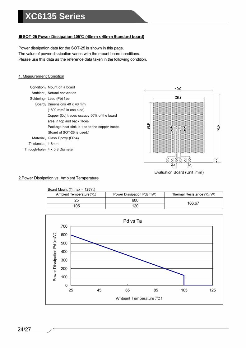
SOT-25 Power Dissipation 105 (40mm x 40mm Standard board)
Power dissipation data for the SOT-25 is shown in this page.The value of power dissipation varies with the mount board conditions.Please use this data as the reference data taken in the following condition.
1. Measurement Condition
Condition: Mount on a boardAmbient: Natural convection
Soldering: Lead (Pb) freeBoard: Dimensions 40 x 40 mm
(1600 mm2 in one side) Copper (Cu) traces occupy 50% of the boardarea In top and back facesPackage heat-sink is tied to the copper traces(Board of SOT-26 is used.)
Material: Glass Epoxy (FR-4) Thickness: 1.6mm
Through-hole: 4 x 0.8 Diameter
Evaluation Board (Unit:mm)2.Power Dissipation vs. Ambient Temperature
Board Mount (Tj max = 125)Ambient Temperature() Power Dissipation Pd(mW) Thermal Resistance (/W)
25 600166.67105 120
0
100
200
300
400
500
600
700
25 45 65 85 105 125
Pow
er D
issi
patio
n Pd
(m
W)
Ambient Temperature()
Pd vs Ta
25/27
XC6135Series
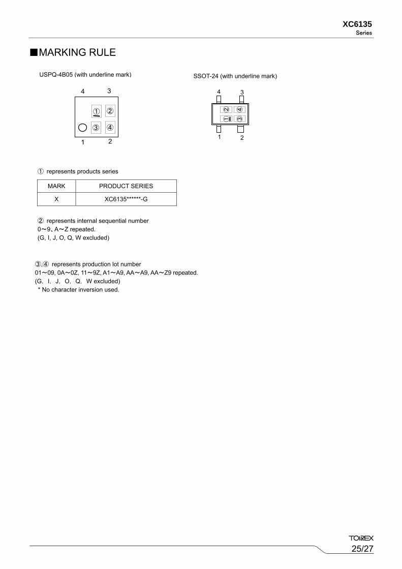
MARKING RULE
MARK PRODUCT SERIES
X XC6135******-G
③,④ represents production lot number 01~09, 0A~0Z, 11~9Z, A1~A9, AA~A9, AA~Z9 repeated. (G,I,J,O,Q,W excluded) * No character inversion used.
USPQ-4B05 (with underline mark) SSOT-24 (with underline mark)
③ ④
① ②
1 2
4 3
④
1 2
34
③
②①
① represents products series
② represents internal sequential number 0~9、A~Z repeated. (G, I, J, O, Q, W excluded)
26/27
XC6135 Series
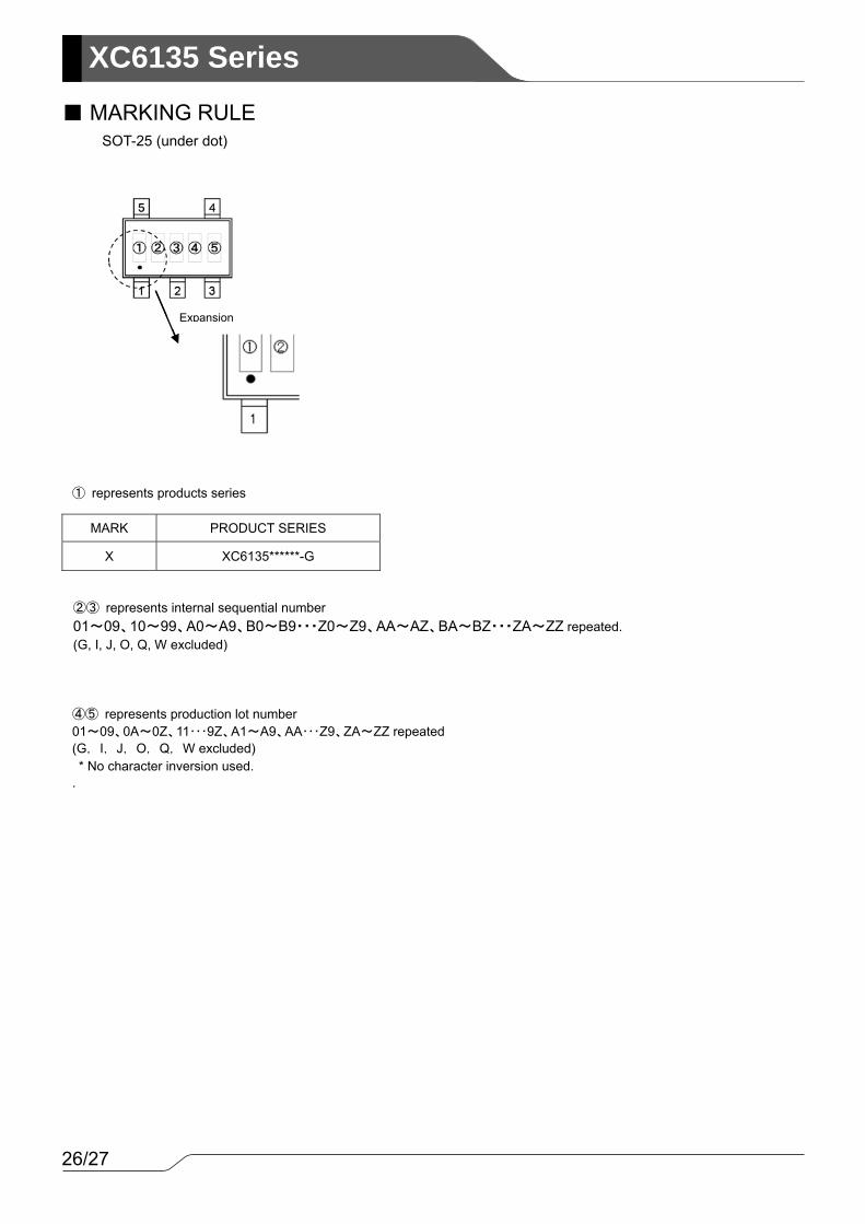
MARKING RULE
MARK PRODUCT SERIES
X XC6135******-G
SOT-25 (under dot)
① represents products series
②③ represents internal sequential number 01~09、10~99、A0~A9、B0~B9・・・Z0~Z9、AA~AZ、BA~BZ・・・ZA~ZZ repeated. (G, I, J, O, Q, W excluded)
④⑤ represents production lot number 01~09、0A~0Z、11・・・9Z、A1~A9、AA・・・Z9、ZA~ZZ repeated (G,I,J,O,Q,W excluded) * No character inversion used.
.
Expansion
27/27
XC6135Series
1. The product and product specifications contained herein are subject to change without notice to improve performance characteristics. Consult us, or our representatives before use, to confirm that the information in this datasheet is up to date.
2. The information in this datasheet is intended to illustrate the operation and characteristics of our
products. We neither make warranties or representations with respect to the accuracy or completeness of the information contained in this datasheet nor grant any license to any intellectual property rights of ours or any third party concerning with the information in this datasheet.
3. Applicable export control laws and regulations should be complied and the procedures required by
such laws and regulations should also be followed, when the product or any information contained in this datasheet is exported.
4. The product is neither intended nor warranted for use in equipment of systems which require
extremely high levels of quality and/or reliability and/or a malfunction or failure which may cause loss of human life, bodily injury, serious property damage including but not limited to devices or equipment used in 1) nuclear facilities, 2) aerospace industry, 3) medical facilities, 4) automobile industry and other transportation industry and 5) safety devices and safety equipment to control combustions and explosions. Do not use the product for the above use unless agreed by us in writing in advance.
5. Although we make continuous efforts to improve the quality and reliability of our products;
nevertheless Semiconductors are likely to fail with a certain probability. So in order to prevent personal injury and/or property damage resulting from such failure, customers are required to incorporate adequate safety measures in their designs, such as system fail safes, redundancy and fire prevention features.
6. Our products are not designed to be Radiation-resistant.
7. Please use the product listed in this datasheet within the specified ranges.
8. We assume no responsibility for damage or loss due to abnormal use.
9. All rights reserved. No part of this datasheet may be copied or reproduced unless agreed by Torex
Semiconductor Ltd in writing in advance.
TOREX SEMICONDUCTOR LTD.