Embed Size (px)
Citation preview
XAUI v12.1
LogiCORE IP Product Guide
Vivado Design Suite
PG053 November 19, 2014
XAUI v12.1 Product Guide www.xilinx.com 2PG053 November 19, 2014
Table of ContentsIP Facts
Chapter 1: OverviewAdditional Features . . . . . . . . . . . . . . . . . . . . . . . . . . . . . . . . . . . . . . . . . . . . . . . . . . . . . . . . . . . . . . . . 8About the Core . . . . . . . . . . . . . . . . . . . . . . . . . . . . . . . . . . . . . . . . . . . . . . . . . . . . . . . . . . . . . . . . . . . . 8Recommended Design Experience . . . . . . . . . . . . . . . . . . . . . . . . . . . . . . . . . . . . . . . . . . . . . . . . . . . . 8Applications . . . . . . . . . . . . . . . . . . . . . . . . . . . . . . . . . . . . . . . . . . . . . . . . . . . . . . . . . . . . . . . . . . . . . . 9Licensing and Ordering Information . . . . . . . . . . . . . . . . . . . . . . . . . . . . . . . . . . . . . . . . . . . . . . . . . . 10Feedback. . . . . . . . . . . . . . . . . . . . . . . . . . . . . . . . . . . . . . . . . . . . . . . . . . . . . . . . . . . . . . . . . . . . . . . . 11
Chapter 2: Product SpecificationStandards Compliance . . . . . . . . . . . . . . . . . . . . . . . . . . . . . . . . . . . . . . . . . . . . . . . . . . . . . . . . . . . . . 12Performance. . . . . . . . . . . . . . . . . . . . . . . . . . . . . . . . . . . . . . . . . . . . . . . . . . . . . . . . . . . . . . . . . . . . . 12Resource Utilization. . . . . . . . . . . . . . . . . . . . . . . . . . . . . . . . . . . . . . . . . . . . . . . . . . . . . . . . . . . . . . . 13Verification . . . . . . . . . . . . . . . . . . . . . . . . . . . . . . . . . . . . . . . . . . . . . . . . . . . . . . . . . . . . . . . . . . . . . . 15Port Descriptions . . . . . . . . . . . . . . . . . . . . . . . . . . . . . . . . . . . . . . . . . . . . . . . . . . . . . . . . . . . . . . . . . 16Register Space . . . . . . . . . . . . . . . . . . . . . . . . . . . . . . . . . . . . . . . . . . . . . . . . . . . . . . . . . . . . . . . . . . . 34
Chapter 3: Designing with the CoreUse the Example Design as a Starting Point. . . . . . . . . . . . . . . . . . . . . . . . . . . . . . . . . . . . . . . . . . . . 37Know the Degree of Difficulty. . . . . . . . . . . . . . . . . . . . . . . . . . . . . . . . . . . . . . . . . . . . . . . . . . . . . . . 37Keep It Registered . . . . . . . . . . . . . . . . . . . . . . . . . . . . . . . . . . . . . . . . . . . . . . . . . . . . . . . . . . . . . . . . 38Recognize Timing Critical Signals . . . . . . . . . . . . . . . . . . . . . . . . . . . . . . . . . . . . . . . . . . . . . . . . . . . . 38Use Supported Design Flows. . . . . . . . . . . . . . . . . . . . . . . . . . . . . . . . . . . . . . . . . . . . . . . . . . . . . . . . 38Make Only Allowed Modifications . . . . . . . . . . . . . . . . . . . . . . . . . . . . . . . . . . . . . . . . . . . . . . . . . . . 38
Chapter 4: Core ArchitectureSystem Overview . . . . . . . . . . . . . . . . . . . . . . . . . . . . . . . . . . . . . . . . . . . . . . . . . . . . . . . . . . . . . . . . . 39Functional Description. . . . . . . . . . . . . . . . . . . . . . . . . . . . . . . . . . . . . . . . . . . . . . . . . . . . . . . . . . . . . 41
Chapter 5: Interfacing to the CoreData Interface: Internal XGMII Interfaces . . . . . . . . . . . . . . . . . . . . . . . . . . . . . . . . . . . . . . . . . . . . . 43Interfacing to the Transmit Client Interface. . . . . . . . . . . . . . . . . . . . . . . . . . . . . . . . . . . . . . . . . . . . 45
Send Feedback
XAUI v12.1 Product Guide www.xilinx.com 3PG053 November 19, 2014
Interfacing to the Receive Client Interface. . . . . . . . . . . . . . . . . . . . . . . . . . . . . . . . . . . . . . . . . . . . . 47Configuration and Status Interfaces . . . . . . . . . . . . . . . . . . . . . . . . . . . . . . . . . . . . . . . . . . . . . . . . . . 49MDIO Interface. . . . . . . . . . . . . . . . . . . . . . . . . . . . . . . . . . . . . . . . . . . . . . . . . . . . . . . . . . . . . . . . . . . 49Configuration and Status Vectors . . . . . . . . . . . . . . . . . . . . . . . . . . . . . . . . . . . . . . . . . . . . . . . . . . . . 95Debug Port . . . . . . . . . . . . . . . . . . . . . . . . . . . . . . . . . . . . . . . . . . . . . . . . . . . . . . . . . . . . . . . . . . . . . . 97
Chapter 6: Design ConsiderationsShared Logic . . . . . . . . . . . . . . . . . . . . . . . . . . . . . . . . . . . . . . . . . . . . . . . . . . . . . . . . . . . . . . . . . . . . . 98Clocking: UltraScale Architecture . . . . . . . . . . . . . . . . . . . . . . . . . . . . . . . . . . . . . . . . . . . . . . . . . . . . 99Clocking: Zynq-7000, Virtex-7, Artix-7, and Kintex-7 Devices . . . . . . . . . . . . . . . . . . . . . . . . . . . . . 100Multiple Core Instances. . . . . . . . . . . . . . . . . . . . . . . . . . . . . . . . . . . . . . . . . . . . . . . . . . . . . . . . . . . 109Reset Circuits . . . . . . . . . . . . . . . . . . . . . . . . . . . . . . . . . . . . . . . . . . . . . . . . . . . . . . . . . . . . . . . . . . . 109Receiver Termination: Virtex-7 and Kintex-7 FPGAs . . . . . . . . . . . . . . . . . . . . . . . . . . . . . . . . . . . . 109Transmit Skew . . . . . . . . . . . . . . . . . . . . . . . . . . . . . . . . . . . . . . . . . . . . . . . . . . . . . . . . . . . . . . . . . . 110
Chapter 7: Design Flow StepsCustomizing and Generating the Core . . . . . . . . . . . . . . . . . . . . . . . . . . . . . . . . . . . . . . . . . . . . . . . 111Output Generation. . . . . . . . . . . . . . . . . . . . . . . . . . . . . . . . . . . . . . . . . . . . . . . . . . . . . . . . . . . . . . . 114Constraining the Core . . . . . . . . . . . . . . . . . . . . . . . . . . . . . . . . . . . . . . . . . . . . . . . . . . . . . . . . . . . . 114Simulation . . . . . . . . . . . . . . . . . . . . . . . . . . . . . . . . . . . . . . . . . . . . . . . . . . . . . . . . . . . . . . . . . . . . . 116Synthesis and Implementation . . . . . . . . . . . . . . . . . . . . . . . . . . . . . . . . . . . . . . . . . . . . . . . . . . . . . 117
Chapter 8: Detailed Example Design
Chapter 9: Test Bench
Appendix A: Verification and InteroperabilitySimulation . . . . . . . . . . . . . . . . . . . . . . . . . . . . . . . . . . . . . . . . . . . . . . . . . . . . . . . . . . . . . . . . . . . . . 124Hardware Testing. . . . . . . . . . . . . . . . . . . . . . . . . . . . . . . . . . . . . . . . . . . . . . . . . . . . . . . . . . . . . . . . 124
Appendix B: Migrating and UpgradingDevice Migration . . . . . . . . . . . . . . . . . . . . . . . . . . . . . . . . . . . . . . . . . . . . . . . . . . . . . . . . . . . . . . . . 125Migrating to the Vivado Design Suite. . . . . . . . . . . . . . . . . . . . . . . . . . . . . . . . . . . . . . . . . . . . . . . . 125Upgrading in the Vivado Design Suite . . . . . . . . . . . . . . . . . . . . . . . . . . . . . . . . . . . . . . . . . . . . . . . 125
Appendix C: Debugging DesignsFinding Help on xilinx.com . . . . . . . . . . . . . . . . . . . . . . . . . . . . . . . . . . . . . . . . . . . . . . . . . . . . . . . . 132Contacting Technical Support . . . . . . . . . . . . . . . . . . . . . . . . . . . . . . . . . . . . . . . . . . . . . . . . . . . . . . 133Debug Tools . . . . . . . . . . . . . . . . . . . . . . . . . . . . . . . . . . . . . . . . . . . . . . . . . . . . . . . . . . . . . . . . . . . . 134Simulation Specific Debug. . . . . . . . . . . . . . . . . . . . . . . . . . . . . . . . . . . . . . . . . . . . . . . . . . . . . . . . . 134
Send Feedback
XAUI v12.1 Product Guide www.xilinx.com 4PG053 November 19, 2014
Hardware Debug . . . . . . . . . . . . . . . . . . . . . . . . . . . . . . . . . . . . . . . . . . . . . . . . . . . . . . . . . . . . . . . . 136
Appendix D: Additional Resources and Legal NoticesXilinx Resources . . . . . . . . . . . . . . . . . . . . . . . . . . . . . . . . . . . . . . . . . . . . . . . . . . . . . . . . . . . . . . . . . 146References . . . . . . . . . . . . . . . . . . . . . . . . . . . . . . . . . . . . . . . . . . . . . . . . . . . . . . . . . . . . . . . . . . . . . 146Additional Core Resources . . . . . . . . . . . . . . . . . . . . . . . . . . . . . . . . . . . . . . . . . . . . . . . . . . . . . . . . 147Revision History . . . . . . . . . . . . . . . . . . . . . . . . . . . . . . . . . . . . . . . . . . . . . . . . . . . . . . . . . . . . . . . . . 147Please Read: Important Legal Notices . . . . . . . . . . . . . . . . . . . . . . . . . . . . . . . . . . . . . . . . . . . . . . . 148
Send Feedback
XAUI v12.1 Product Guide www.xilinx.com 5PG053 November 19, 2014 Product Specification
IntroductionThe Xilinx® LogiCORE™ IP eXtended Attachment Unit Interface (XAUI) core is a high-performance, low-pin count 10-Gb/s interface intended to allow physical separation between the data link layer and physical layer devices in a 10-Gigabit Ethernet system.
The XAUI core implements a single-speed full-duplex 10-Gb/s Ethernet eXtended Attachment Unit Interface (XAUI) solution for the UltraScale™ architecture (GTHE3 transceivers), Zynq®-7000 All Programmable SoC, and 7-series devices.
Features• Designed to 10-Gigabit Ethernet IEEE
802.3-2012 specif ication
• Supports 20G double-rate XAUI (Double XAUI) using four transceivers at 6.25 Gb/s. For devices and speed grades, see Speed Grades.
• Supports 10-Gigabit Fiber Channel (10-GFC) XAUI data rates and traffic
• Uses four transceivers at 3.125 Gb/s line rate to achieve 10-Gb/s data rate
• Implements Data Terminal Equipment (DTE) XGMII Extender Sublayer (XGXS), PHY XGXS, and 10GBASE-X Physical Coding Sublayer (PCS) in a single netlist
• IEEE 802.3-2012 clause 45 Management Data Input/Output (MDIO) interface (optional)
• IEEE 802.3-2012 clause 48 State Machines
• Available under the Xilinx End User License Agreement
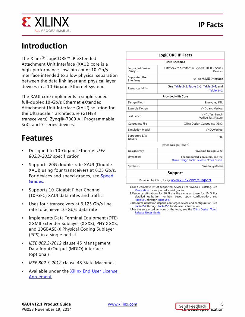
IP Facts
LogiCORE IP FactsCore Specifics
Supported Device Family(1)
1.For a complete list of supported devices, see Vivado IP catalog. SeeVerification for supported speed grades.
UltraScale™ Architecture, Zynq®-7000, 7 SeriesDevices
Supported User Interfaces 64-bit XGMII Interface
Resources (2), (3)
2.Resource utilizations for 20 G are the same as those for 10 G. Fordetailed utilization numbers based upon configuration, seeTable 2-2 through Table 2-5.
3.Resource utilization depends on target device and configuration. SeeTable 2-2 through Table 2-5 for detailed information.
See Table 2-2, Table 2-3, Table 2-4, andTable 2-5.
Provided with Core
Design Files Encrypted RTL
Example Design VHDL and Verilog
Test Bench VHDL Test BenchVerilog Test Fixture
Constraints File Xilinx Design Constraints (XDC)
Simulation Model VHDL/Verilog
Supported S/W Drivers NA
Tested Design Flows(4)
4.For the supported versions of the tools, see the Xilinx Design Tools:Release Notes Guide.
Design Entry Vivado® Design Suite
Simulation For supported simulators, see theXilinx Design Tools: Release Notes Guide.
Synthesis Vivado Synthesis
Support
Provided by Xilinx, Inc.@ www.xilinx.com/support
Send Feedback
XAUI v12.1 Product Guide www.xilinx.com 6PG053 November 19, 2014
Chapter 1
OverviewXAUI is a four-lane, 3.125 Gb/s-per-lane serial interface. Each lane is a differential pair carrying current mode logic (CML) signaling, and the data on each lane is 8B/10B encoded before transmission. Special code groups are used to allow each lane to synchronize at a word boundary and to deskew all four lanes into alignment at the receiving end. The XAUI standard is fully specif ied in clauses 47 and 48 of the 10-Gigabit Ethernet IEEE 802.3-2012 specification.
The XAUI standard was initially developed as a means to extend the physical separation possible between Media Access Controller (MAC) and PHY components in a 10-Gigabit Ethernet system distributed across a circuit board and to reduce the number of interface signals in comparison with the XGMII (10-Gigabit Ethernet Media Independent Interface).
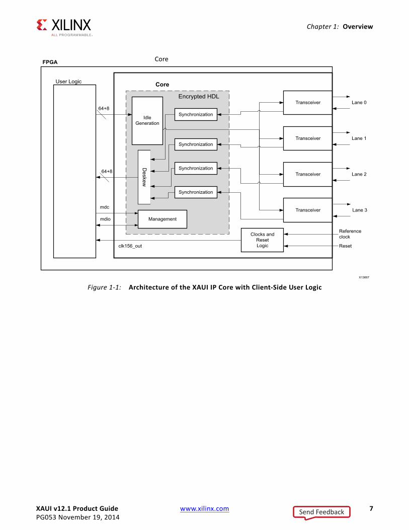
Figure 1-1 shows a block diagram of the XAUI core implementation. The major functional blocks of the core include the following:
• Transmit Idle Generation Logic creates the code groups to allow synchronization and alignment at the receiver.
• Synchronization State Machine (one per lane) identif ies byte boundaries in incoming serial data.
• Deskew State Machine de-skews the four received lanes into alignment.
• Optional MDIO Interface is a two-wire low-speed serial interface used to manage the core.
• Four Device-Specific Transceivers (integrated in the FPGAs) provide the high-speed transceivers as well as 8B/10B encode and decode and elastic buffering in the receive datapath.
Send Feedback
XAUI v12.1 Product Guide www.xilinx.com 7PG053 November 19, 2014
Chapter 1: Overview
X-Ref Target - Figure 1-1
Figure 1-1: Architecture of the XAUI IP Core with Client-Side User Logic
Send Feedback
XAUI v12.1 Product Guide www.xilinx.com 8PG053 November 19, 2014
Chapter 1: Overview
Additional Features
10-Gigabit Fiber Channel SupportThe 10-Gigabit Fiber Channel (10GFC) specif ication describes a XAUI interface similar to the 10-Gigabit Ethernet XAUI but operating at 2% higher line and data rates, equating to a line rate on each device-specif ic transceiver lane of 3.1875 Gb/s.
20-Gigabit XAUI (Double XAUI) SupportBy running the XAUI interface at twice the normal clock and line rates, 20-Gigabit data rate can be achieved. For devices and speed grades, see Speed Grades. Consult the release notes for the core for the specific devices supported.
About the CoreThe XAUI core is a Xilinx® Intellectual Property (IP) core, included in the latest IP Update on the Xilinx IP Center. For detailed information about the core, see the XAUI product page.
Recommended Design ExperienceAlthough the XAUI core is a fully-verif ied solution, the challenge associated with implementing a complete design varies depending on the configuration and functionality of the application. For best results, previous experience building high performance, pipelined Field Programmable Gate Array (FPGA) designs using Xilinx implementation software and Xilinx Design Constraints (XDC) is recommended.
Contact your local Xilinx representative for a closer review and estimation for your specific requirements.
Send Feedback
XAUI v12.1 Product Guide www.xilinx.com 9PG053 November 19, 2014
Chapter 1: Overview
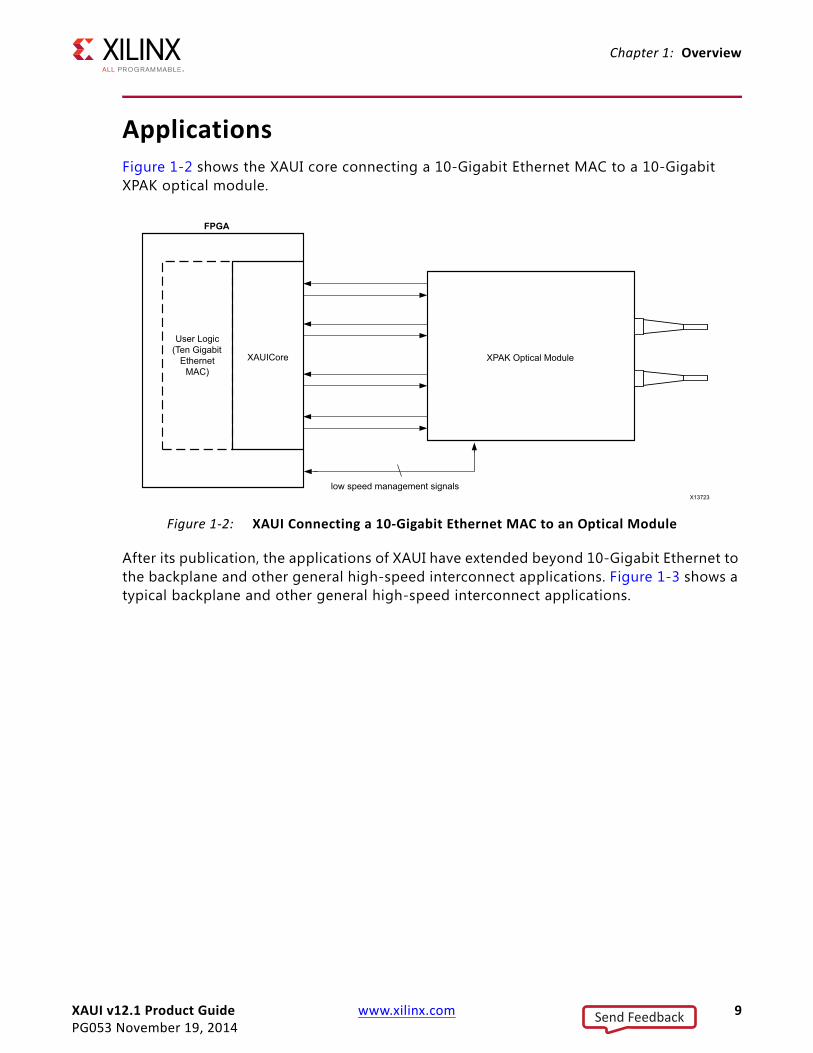
ApplicationsFigure 1-2 shows the XAUI core connecting a 10-Gigabit Ethernet MAC to a 10-Gigabit XPAK optical module.
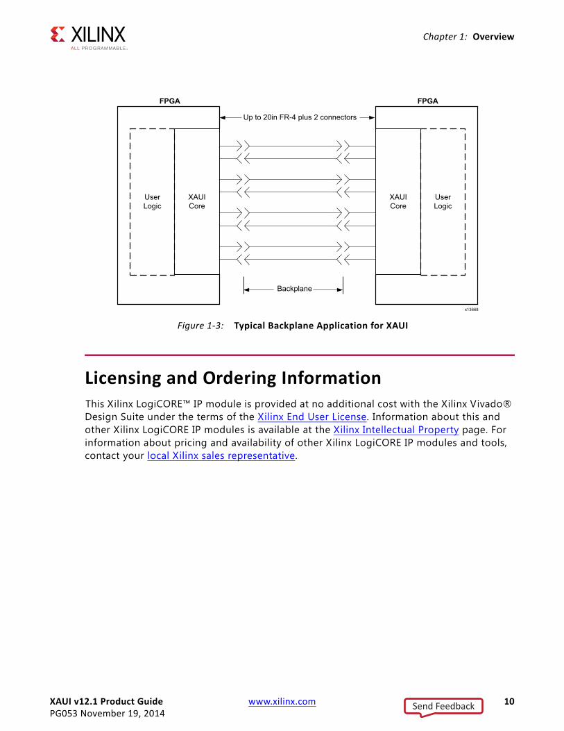
After its publication, the applications of XAUI have extended beyond 10-Gigabit Ethernet to the backplane and other general high-speed interconnect applications. Figure 1-3 shows a typical backplane and other general high-speed interconnect applications.
X-Ref Target - Figure 1-2
Figure 1-2: XAUI Connecting a 10-Gigabit Ethernet MAC to an Optical Module
Send Feedback
XAUI v12.1 Product Guide www.xilinx.com 10PG053 November 19, 2014
Chapter 1: Overview
Licensing and Ordering InformationThis Xilinx LogiCORE™ IP module is provided at no additional cost with the Xilinx Vivado® Design Suite under the terms of the Xilinx End User License. Information about this and other Xilinx LogiCORE IP modules is available at the Xilinx Intellectual Property page. For information about pricing and availability of other Xilinx LogiCORE IP modules and tools, contact your local Xilinx sales representative.
X-Ref Target - Figure 1-3
Figure 1-3: Typical Backplane Application for XAUI
Send Feedback
XAUI v12.1 Product Guide www.xilinx.com 11PG053 November 19, 2014
Chapter 1: Overview
FeedbackXilinx welcomes comments and suggestions about the XAUI core and the documentation supplied with the core.
CoreFor comments or suggestions about the XAUI core, submit a webcase from www.xilinx.com/support. Be sure to include the following information:
• Product name
• Core version number
• Explanation of your comments
DocumentFor comments or suggestions about this document, submit a webcase from www.xilinx.com/support. Be sure to include the following information:
• Document title
• Document number
• Page number(s) to which your comments refer
• Explanation of your comments
Send Feedback
XAUI v12.1 Product Guide www.xilinx.com 12PG053 November 19, 2014
Chapter 2
Product Specification
Standards ComplianceThe XAUI IP core is designed to the standard specified in clauses 47 and 48 of the 10-Gigabit Ethernet specification IEEE Std. 802.3-2012.
PerformanceThis section contains the following subsections:
• Latency
• Speed Grades
LatencyThese measurements are for the core only; they do not include the latency through the transceiver. The latency through the transceiver can be obtained from the relevant transceiver user guide.
Transmit Path Latency
As measured from the input port xgmii_txd[63:0] of the transmitter side XGMII (until that data appears on the txdata pins on the internal transceiver interface on the transceiver interface), the latency through the core for the internal XGMII interface configuration in the transmit direction is four clk periods of the core input usrclk .
Send Feedback
XAUI v12.1 Product Guide www.xilinx.com 13PG053 November 19, 2014
Chapter 2: Product Specification
Receive Path Latency
Measured from the input into the core encrypted hdl logic from the rxdata pins of the internal transceiver interface until the data appears on xgmii_rxdata[63:0] of the receiver side XGMII interface, the latency through the core in the receive direction is equal to 4–5 clock cycles of usrclk .
If the word appears on the upper half of the two-byte transceiver interface, the latency is f ive clock cycles of usrclk and it appears on the lower half of the XGMII interface. If it appears on the lower half of the two-byte interface, the latency is four clock cycles of usrclk and it appears on the upper half of the XGMII interface.
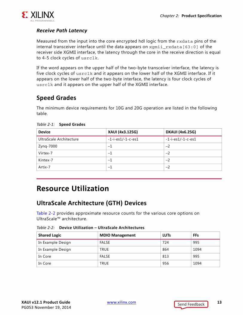
Speed GradesThe minimum device requirements for 10G and 20G operation are listed in the following table.
Resource Utilization
UltraScale Architecture (GTH) DevicesTable 2-2 provides approximate resource counts for the various core options on UltraScale™ architecture.
Table 2-1: Speed Grades
Device XAUI (4x3.125G) DXAUI (4x6.25G)
UltraScale Architecture -1-i-es1/-1-c-es1 -1-i-es1/-1-c-es1
Zynq-7000 –1 –2
Virtex-7 –1 –2
Kintex-7 –1 –2
Artix-7 –1 –2
Table 2-2: Device Utilization – UltraScale Architectures
Shared Logic MDIO Management LUTs FFs
In Example Design FALSE 724 995
In Example Design TRUE 864 1094
In Core FALSE 813 995
In Core TRUE 956 1094
Send Feedback
XAUI v12.1 Product Guide www.xilinx.com 14PG053 November 19, 2014
Chapter 2: Product Specification
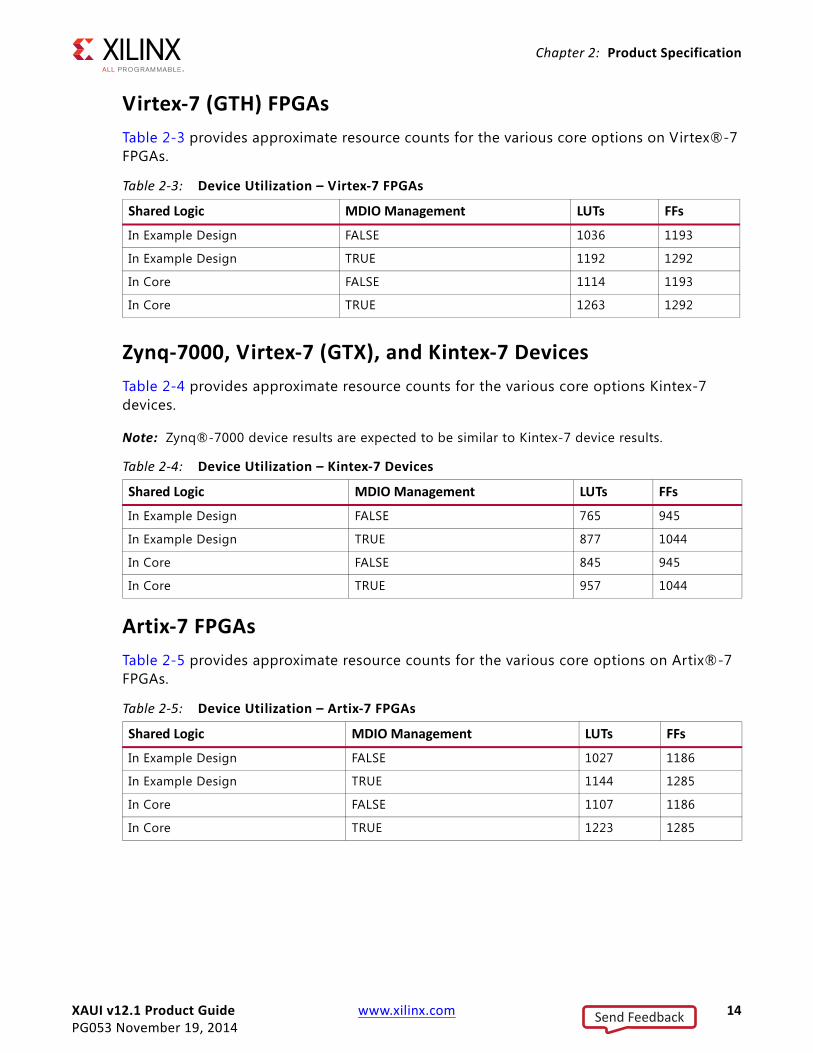
Virtex-7 (GTH) FPGAsTable 2-3 provides approximate resource counts for the various core options on Virtex®-7 FPGAs.
Zynq-7000, Virtex-7 (GTX), and Kintex-7 DevicesTable 2-4 provides approximate resource counts for the various core options Kintex-7 devices.
Note: Zynq®-7000 device results are expected to be similar to Kintex-7 device results..
Artix-7 FPGAsTable 2-5 provides approximate resource counts for the various core options on Artix®-7 FPGAs.
Table 2-3: Device Utilization – Virtex-7 FPGAs
Shared Logic MDIO Management LUTs FFs
In Example Design FALSE 1036 1193
In Example Design TRUE 1192 1292
In Core FALSE 1114 1193
In Core TRUE 1263 1292
Table 2-4: Device Utilization – Kintex-7 Devices
Shared Logic MDIO Management LUTs FFs
In Example Design FALSE 765 945
In Example Design TRUE 877 1044
In Core FALSE 845 945
In Core TRUE 957 1044
Table 2-5: Device Utilization – Artix-7 FPGAs
Shared Logic MDIO Management LUTs FFs
In Example Design FALSE 1027 1186
In Example Design TRUE 1144 1285
In Core FALSE 1107 1186
In Core TRUE 1223 1285
Send Feedback
XAUI v12.1 Product Guide www.xilinx.com 15PG053 November 19, 2014
Chapter 2: Product Specification
VerificationThe XAUI core has been verif ied using both simulation and hardware testing.
SimulationA highly parameterizable transaction-based simulation test suite was used to verify the core. Verif ication tests include:
• Register access over MDIO
• Loss and regain of synchronization
• Loss and regain of alignment
• Frame transmission
• Frame reception
• Clock compensation
• Recovery from error conditions
Hardware VerificationThe core has been used in several hardware test platforms within Xilinx. In particular, the core has been used in a test platform design with the Xilinx® 10-Gigabit Ethernet MAC. This design comprises the MAC, XAUI, a ping loopback First In First Out (FIFO), and a test pattern generator all under embedded processor control. This design has been used for conformance and interoperability testing at the University of New Hampshire Interoperability Lab.
Send Feedback
XAUI v12.1 Product Guide www.xilinx.com 16PG053 November 19, 2014
Chapter 2: Product Specification
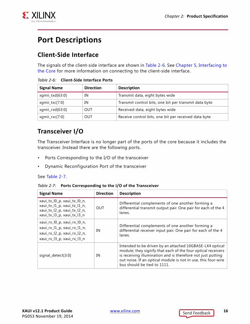
Port Descriptions
Client-Side InterfaceThe signals of the client-side interface are shown in Table 2-6. See Chapter 5, Interfacing to the Core for more information on connecting to the client-side interface.
Transceiver I/OThe Transceiver Interface is no longer part of the ports of the core because it includes the transceiver. Instead there are the following ports.
• Ports Corresponding to the I/O of the transceiver
• Dynamic Reconfiguration Port of the transceiver
See Table 2-7.
Table 2-6: Client-Side Interface Ports
Signal Name Direction Description
xgmii_txd[63:0] IN Transmit data, eight bytes wide
xgmii_txc[7:0] IN Transmit control bits, one bit per transmit data byte
xgmii_rxd[63:0] OUT Received data, eight bytes wide
xgmii_rxc[7:0] OUT Receive control bits, one bit per received data byte
Table 2-7: Ports Corresponding to the I/O of the Transceiver
Signal Name Direction Description
xaui_tx_l0_p, xaui_tx_l0_n, xaui_tx_l1_p, xaui_tx_l1_n, xaui_tx_l2_p, xaui_tx_l2_n, xaui_tx_l3_p, xaui_tx_l3_n
OUTDifferential complements of one another forming a differential transmit output pair. One pair for each of the 4 lanes.
xaui_rx_l0_p, xaui_rx_l0_n,xaui_rx_l1_p, xaui_rx_l1_n,xaui_rx_l2_p, xaui_rx_l2_n,xaui_rx_l3_p, xaui_rx_l3_n
INDifferential complements of one another forming a differential receiver input pair. One pair for each of the 4 lanes.
signal_detect[3:0] IN
Intended to be driven by an attached 10GBASE-LX4 optical module; they signify that each of the four optical receivers is receiving illumination and is therefore not just putting out noise. If an optical module is not in use, this four-wire bus should be tied to 1111.
Send Feedback
XAUI v12.1 Product Guide www.xilinx.com 17PG053 November 19, 2014
Chapter 2: Product Specification
Transceiver Control and Status PortsOptional ports that, if enabled, allow the monitoring and control of certain important ports of the transceivers. When not selected, these ports are tied to their default values. For information on these ports, see the 7 Series FPGAs GTX/GTH Transceivers User Guide (UG476) [Ref 1], the 7 Series FPGAs GTP Transceivers User Guide (UG482) [Ref 2], and the UltraScale Architecture GTH Transceivers User Guide (UG576) [Ref 3].
Note: The Dynamic Reconfiguration Port is only available if the Transceiver Control and Status Ports option is selected
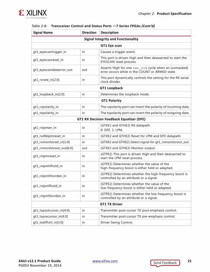
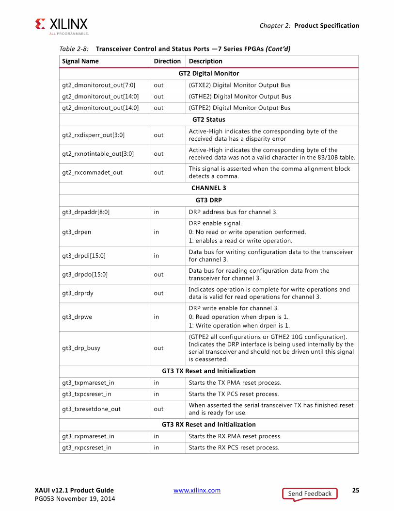
Table 2-8: Transceiver Control and Status Ports —7 Series FPGAs
Signal Name Direction Description
CHANNEL 0
GT0 DRP
gt0_drpaddr[8:0] in DRP address bus for channel 0
gt0_drpen inDRP enable signal. 0: No read or write operation performed. 1: enables a read or write operation.
gt0_drpdi[15:0] in Data bus for writing configuration data to the transceiver for channel 0.
gt0_drpdo[15:0] out Data bus for reading configuration data from the transceiver for channel 0.
gt0_drprdy out Indicates operation is complete for write operations and data is valid for read operations for channel 0.
gt0_drpwe inDRP write enable for channel 0. 0: Read operation when drpen is 1. 1: Write operation when drpen is 1.
gt0_drp_busy out
(GTPE2 all configurations or GTHE2 10G configuration). Indicates the DRP interface is being used internally by the serial transceiver and should not be driven until this signal is deasserted.
GT0 TX Reset and Initialization
gt0_txpmareset_in in Starts the TX PMA reset process.
gt0_txpcsreset_in in Starts the TX PCS reset process.
gt0_txresetdone_out out When asserted the serial transceiver TX has finished reset and is ready for use.
GT0 RX Reset and Initialization
gt0_rxpmareset_in in Starts the RX PMA reset process.
gt0_rxpcsreset_in in Starts the RX PCS reset process.
gt0_rxpmaresetdone_out out (GTHE2 and GTPE2) This active-High signal indicates RX PMA reset is complete.
gt0_rxresetdone_out out When asserted the serial transceiver RX has f inished reset and is ready for use.
Send Feedback
XAUI v12.1 Product Guide www.xilinx.com 18PG053 November 19, 2014
Chapter 2: Product Specification
GT0 Clocking
gt0_rxbufstatus_out[2:0] out RX buffer status.
gt0_txphaligndone_out out TX phase alignment done.
gt0_txphinitdone_out out TX phase alignment initialization done.
gt0_txdlysresetdone_out out TX delay alignment soft reset done.
gt0_cplllock_out out(GTHE2) This active-High PLL frequency lock signal indicates that the PLL frequency is within predetermined tolerance.
gt_qplllock_out out(GTXE2 and GTPE2) This active-High PLL frequency lock signal indicates that the PLL frequency is within predetermined tolerance.
Signal Integrity and Functionality
GT0 Eye scan
gt0_eyescantrigger_in in Causes a trigger event.
gt0_eyescanreset_in in This port is driven High and then deasserted to start the EYESCAN reset process.
gt0_eyescandataerror_out out Asserts High for one rec_clk cycle when an (unmasked) error occurs while in the COUNT or ARMED state.
gt0_rxrate_in[2:0] in This port dynamically controls the setting for the RX serial clock divider.
GT0 Loopback
gt0_loopback_in[2:0] in Determines the loopback mode.
GT0 Polarity
gt0_rxpolarity_in in The rxpolarity port can invert the polarity of incoming data.
gt0_txpolarity_in in The txpolarity port can invert the polarity of outgoing data.
GT0 RX Decision Feedback Equalizer (DFE)
gt0_rxlpmen_in in(GTXE2 and GTHE2) RX datapath. 0: DFE. 1: LPM.
gt0_rxdfelpmreset_in in (GTXE2 and GTHE2) Reset for LPM and DFE datapath.
gt0_rxmonitorsel_in[1:0] in (GTXE2 and GTHE2) Select signal for gt0_rxmonitorout_out.
gt0_rxmonitorout_out[6:0] out (GTXE2 and GTHE2) Monitor output.
gt0_rxlpmreset_in in (GTPE2) This port is driven High and then deasserted to start the LPM reset process.
gt0_rxlpmhfhold_in in (GTPE2) Determines whether the value of the high-frequency boost is either held or adapted.
gt0_rxlpmhfovrden_in in (GTPE2) Determines whether the high-frequency boost is controlled by an attribute or a signal.
Table 2-8: Transceiver Control and Status Ports —7 Series FPGAs (Cont’d)
Signal Name Direction Description
Send Feedback
XAUI v12.1 Product Guide www.xilinx.com 19PG053 November 19, 2014
Chapter 2: Product Specification
gt0_rxlpmlfhold_in in (GTPE2) Determines whether the value of the low-frequency boost is either held or adapted.
gt0_rxlpmlfovrden_in in (GTPE2) Determines whether the low-frequency boost is controlled by an attribute or a signal.
GT0 TX Driver
gt0_txpostcursor_in[4:0] in Transmitter post-cursor TX post-emphasis control.
gt0_txprecursor_in[4:0] in Transmitter post-cursor TX pre-emphasis control.
gt0_txdiffctrl_in[3:0] in Driver Swing Control.
GT0 PRBS
gt0_rxprbscntreset_in in Resets the PRBS error counter.
gt0_rxprbserr_out out This non-sticky status output indicates that PRBS errors have occurred.
gt0_rxprbssel_in[2:0] in Receiver PRBS checker test pattern control.
gt0_txprbssel_in[2:0] in Transmitter PRBS generator test pattern control.
gt0_txprbsforceerr_in inWhen this port is driven High, errors are forced in the PRBS transmitter. While this port is asserted, the output data pattern contains errors.
GT0 RX CDR
gt0_rxcdrhold_in in Hold the CDR control loop frozen.
GT0 Digital Monitor
gt0_dmonitorout_out[7:0] out (GTXE2) Digital Monitor Output Bus
gt0_dmonitorout_out[14:0] out (GTHE2) Digital Monitor Output Bus
gt0_dmonitorout_out[14:0] out (GTPE2) Digital Monitor Output Bus
GT0 Status
gt0_rxdisperr_out[3:0] out Active-High indicates the corresponding byte of the received data has a disparity error
gt0_rxnotintable_out[3:0] out Active-High indicates the corresponding byte of the received data was not a valid character in the 8B/10B table.
gt0_rxcommadet_out out This signal is asserted when the comma alignment block detects a comma.
Table 2-8: Transceiver Control and Status Ports —7 Series FPGAs (Cont’d)
Signal Name Direction Description
Send Feedback
XAUI v12.1 Product Guide www.xilinx.com 20PG053 November 19, 2014
Chapter 2: Product Specification
CHANNEL 1
GT1 DRP
gt1_drpaddr[8:0] in DRP address bus for channel 1.
gt1_drpen inDRP enable signal. 0: No read or write operation performed. 1: enables a read or write operation.
gt1_drpdi[15:0] in Data bus for writing configuration data to the transceiver for channel 1.
gt1_drpdo[15:0] out Data bus for reading configuration data from the transceiver for channel 1.
gt1_drprdy out Indicates operation is complete for write operations and data is valid for read operations for channel 1.
gt1_drpwe inDRP write enable for channel 1. 0: Read operation when drpen is 1. 1: Write operation when drpen is 1.
gt1_drp_busy out
(GTPE2 all configurations or GTHE2 10G configuration). Indicates the DRP interface is being used internally by the serial transceiver and should not be driven until this signal is deasserted.
GT1 TX Reset and Initialization
gt1_txpmareset_in in Starts the TX PMA reset process.
gt1_txpcsreset_in in Starts the TX PCS reset process.
gt1_txresetdone_out out When asserted the serial transceiver TX has finished reset and is ready for use.
GT1 RX Reset and Initialization
gt1_rxpmareset_in in Starts the RX PMA reset process.
gt1_rxpcsreset_in in Starts the RX PCS reset process.
gt1_rxpmaresetdone_out out (GTHE2 and GTPE2) This active-High signal indicates RX PMA reset is complete.
gt1_rxresetdone_out out When asserted the serial transceiver RX has f inished reset and is ready for use.
GT1 Clocking
gt1_rxbufstatus_out[2:0] out RX buffer status.
gt1_txphaligndone_out out TX phase alignment done.
gt1_txphinitdone_out out TX phase alignment initialization done.
gt1_txdlysresetdone_out out TX delay alignment soft reset done.
gt1_cplllock_out out(GTHE2) This active-High PLL frequency lock signal indicates that the PLL frequency is within predetermined tolerance.
Table 2-8: Transceiver Control and Status Ports —7 Series FPGAs (Cont’d)
Signal Name Direction Description
Send Feedback
XAUI v12.1 Product Guide www.xilinx.com 21PG053 November 19, 2014
Chapter 2: Product Specification
Signal Integrity and Functionality
GT1 Eye scan
gt1_eyescantrigger_in in Causes a trigger event.
gt1_eyescanreset_in in This port is driven High and then deasserted to start the EYESCAN reset process.
gt1_eyescandataerror_out out Asserts High for one rec_clk cycle when an (unmasked) error occurs while in the COUNT or ARMED state.
gt1_rxrate_in[2:0] in This port dynamically controls the setting for the RX serial clock divider.
GT1 Loopback
gt1_loopback_in[2:0] in Determines the loopback mode.
GT1 Polarity
gt1_rxpolarity_in in The rxpolarity port can invert the polarity of incoming data.
gt1_txpolarity_in in The txpolarity port can invert the polarity of outgoing data.
GT1 RX Decision Feedback Equalizer (DFE)
gt1_rxlpmen_in in(GTXE2 and GTHE2) RX datapath. 0: DFE. 1: LPM.
gt1_rxdfelpmreset_in in (GTXE2 and GTHE2) Reset for LPM and DFE datapath.
gt1_rxmonitorsel_in[1:0] in (GTXE2 and GTHE2) Select signal for gt1_rxmonitorout_out.
gt1_rxmonitorout_out[6:0] out (GTXE2 and GTHE2) Monitor output.
gt1_rxlpmreset_in in (GTPE2) This port is driven High and then deasserted to start the LPM reset process.
gt1_rxlpmhfhold_in in (GTPE2) Determines whether the value of the high-frequency boost is either held or adapted.
gt1_rxlpmhfovrden_in in (GTPE2) Determines whether the high-frequency boost is controlled by an attribute or a signal.
gt1_rxlpmlfhold_in in (GTPE2) Determines whether the value of the low-frequency boost is either held or adapted.
gt1_rxlpmlfovrden_in in (GTPE2) Determines whether the low-frequency boost is controlled by an attribute or a signal.
GT1 TX Driver
gt1_txpostcursor_in[4:0] in Transmitter post-cursor TX post-emphasis control.
gt1_txprecursor_in[4:0] in Transmitter post-cursor TX pre-emphasis control.
gt1_txdiffctrl_in[3:0] in Driver Swing Control.
Table 2-8: Transceiver Control and Status Ports —7 Series FPGAs (Cont’d)
Signal Name Direction Description
Send Feedback
XAUI v12.1 Product Guide www.xilinx.com 22PG053 November 19, 2014
Chapter 2: Product Specification
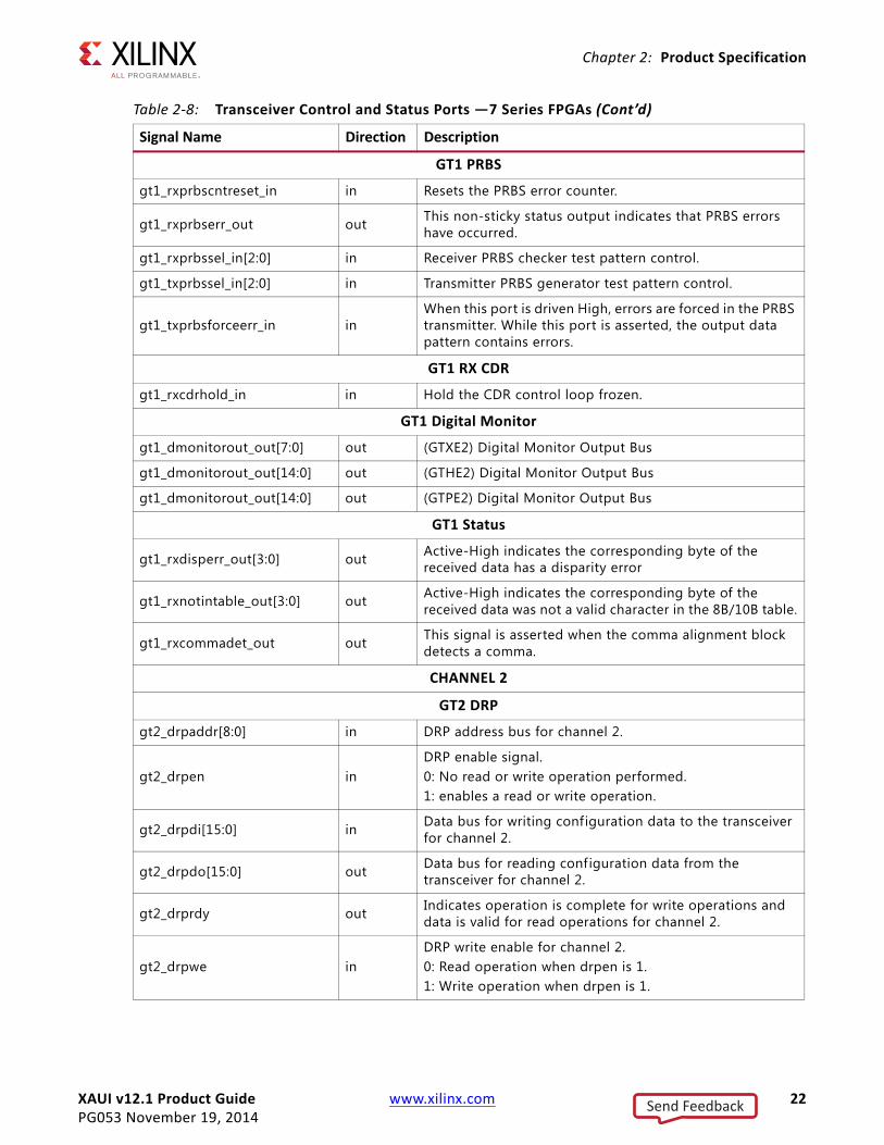
GT1 PRBS
gt1_rxprbscntreset_in in Resets the PRBS error counter.
gt1_rxprbserr_out out This non-sticky status output indicates that PRBS errors have occurred.
gt1_rxprbssel_in[2:0] in Receiver PRBS checker test pattern control.
gt1_txprbssel_in[2:0] in Transmitter PRBS generator test pattern control.
gt1_txprbsforceerr_in inWhen this port is driven High, errors are forced in the PRBS transmitter. While this port is asserted, the output data pattern contains errors.
GT1 RX CDR
gt1_rxcdrhold_in in Hold the CDR control loop frozen.
GT1 Digital Monitor
gt1_dmonitorout_out[7:0] out (GTXE2) Digital Monitor Output Bus
gt1_dmonitorout_out[14:0] out (GTHE2) Digital Monitor Output Bus
gt1_dmonitorout_out[14:0] out (GTPE2) Digital Monitor Output Bus
GT1 Status
gt1_rxdisperr_out[3:0] out Active-High indicates the corresponding byte of the received data has a disparity error
gt1_rxnotintable_out[3:0] out Active-High indicates the corresponding byte of the received data was not a valid character in the 8B/10B table.
gt1_rxcommadet_out out This signal is asserted when the comma alignment block detects a comma.
CHANNEL 2
GT2 DRP
gt2_drpaddr[8:0] in DRP address bus for channel 2.
gt2_drpen inDRP enable signal. 0: No read or write operation performed. 1: enables a read or write operation.
gt2_drpdi[15:0] in Data bus for writing configuration data to the transceiver for channel 2.
gt2_drpdo[15:0] out Data bus for reading configuration data from the transceiver for channel 2.
gt2_drprdy out Indicates operation is complete for write operations and data is valid for read operations for channel 2.
gt2_drpwe inDRP write enable for channel 2. 0: Read operation when drpen is 1. 1: Write operation when drpen is 1.
Table 2-8: Transceiver Control and Status Ports —7 Series FPGAs (Cont’d)
Signal Name Direction Description
Send Feedback
XAUI v12.1 Product Guide www.xilinx.com 23PG053 November 19, 2014
Chapter 2: Product Specification
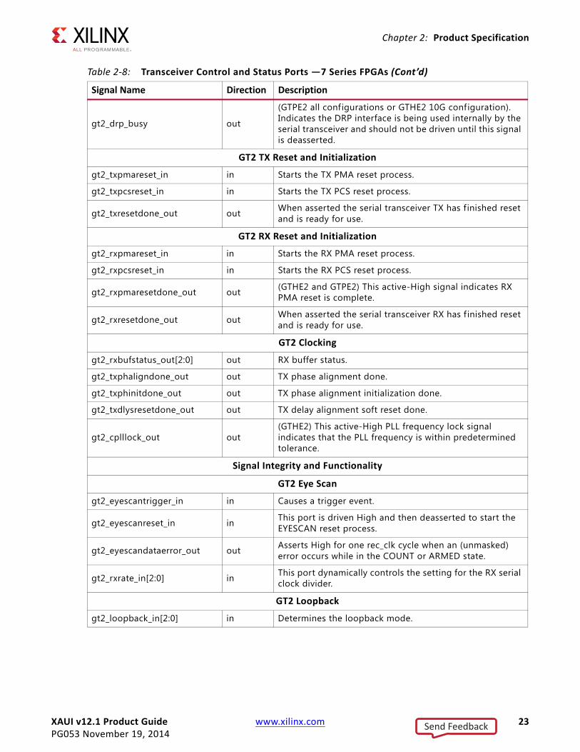
gt2_drp_busy out
(GTPE2 all configurations or GTHE2 10G configuration). Indicates the DRP interface is being used internally by the serial transceiver and should not be driven until this signal is deasserted.
GT2 TX Reset and Initialization
gt2_txpmareset_in in Starts the TX PMA reset process.
gt2_txpcsreset_in in Starts the TX PCS reset process.
gt2_txresetdone_out out When asserted the serial transceiver TX has finished reset and is ready for use.
GT2 RX Reset and Initialization
gt2_rxpmareset_in in Starts the RX PMA reset process.
gt2_rxpcsreset_in in Starts the RX PCS reset process.
gt2_rxpmaresetdone_out out (GTHE2 and GTPE2) This active-High signal indicates RX PMA reset is complete.
gt2_rxresetdone_out out When asserted the serial transceiver RX has f inished reset and is ready for use.
GT2 Clocking
gt2_rxbufstatus_out[2:0] out RX buffer status.
gt2_txphaligndone_out out TX phase alignment done.
gt2_txphinitdone_out out TX phase alignment initialization done.
gt2_txdlysresetdone_out out TX delay alignment soft reset done.
gt2_cplllock_out out(GTHE2) This active-High PLL frequency lock signal indicates that the PLL frequency is within predetermined tolerance.
Signal Integrity and Functionality
GT2 Eye Scan
gt2_eyescantrigger_in in Causes a trigger event.
gt2_eyescanreset_in in This port is driven High and then deasserted to start the EYESCAN reset process.
gt2_eyescandataerror_out out Asserts High for one rec_clk cycle when an (unmasked) error occurs while in the COUNT or ARMED state.
gt2_rxrate_in[2:0] in This port dynamically controls the setting for the RX serial clock divider.
GT2 Loopback
gt2_loopback_in[2:0] in Determines the loopback mode.
Table 2-8: Transceiver Control and Status Ports —7 Series FPGAs (Cont’d)
Signal Name Direction Description
Send Feedback
XAUI v12.1 Product Guide www.xilinx.com 24PG053 November 19, 2014
Chapter 2: Product Specification
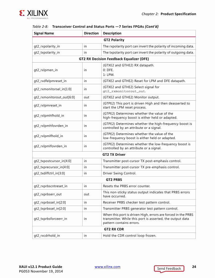
GT2 Polarity
gt2_rxpolarity_in in The rxpolarity port can invert the polarity of incoming data.
gt2_txpolarity_in in The txpolarity port can invert the polarity of outgoing data.
GT2 RX Decision Feedback Equalizer (DFE)
gt2_rxlpmen_in in(GTXE2 and GTHE2) RX datapath. 0: DFE. 1: LPM.
gt2_rxdfelpmreset_in in (GTXE2 and GTHE2) Reset for LPM and DFE datapath.
gt2_rxmonitorsel_in[1:0] in (GTXE2 and GTHE2) Select signal for gt2_rxmonitorout_out.
gt2_rxmonitorout_out[6:0] out (GTXE2 and GTHE2) Monitor output.
gt2_rxlpmreset_in in (GTPE2) This port is driven High and then deasserted to start the LPM reset process.
gt2_rxlpmhfhold_in in (GTPE2) Determines whether the value of the high-frequency boost is either held or adapted.
gt2_rxlpmhfovrden_in in (GTPE2) Determines whether the high-frequency boost is controlled by an attribute or a signal.
gt2_rxlpmlfhold_in in (GTPE2) Determines whether the value of the low-frequency boost is either held or adapted.
gt2_rxlpmlfovrden_in in (GTPE2) Determines whether the low-frequency boost is controlled by an attribute or a signal.
GT2 TX Driver
gt2_txpostcursor_in[4:0] in Transmitter post-cursor TX post-emphasis control.
gt2_txprecursor_in[4:0] in Transmitter post-cursor TX pre-emphasis control.
gt2_txdiffctrl_in[3:0] in Driver Swing Control.
GT2 PRBS
gt2_rxprbscntreset_in in Resets the PRBS error counter.
gt2_rxprbserr_out out This non-sticky status output indicates that PRBS errors have occurred.
gt2_rxprbssel_in[2:0] in Receiver PRBS checker test pattern control.
gt2_txprbssel_in[2:0] in Transmitter PRBS generator test pattern control.
gt2_txprbsforceerr_in inWhen this port is driven High, errors are forced in the PRBS transmitter. While this port is asserted, the output data pattern contains errors.
GT2 RX CDR
gt2_rxcdrhold_in in Hold the CDR control loop frozen.
Table 2-8: Transceiver Control and Status Ports —7 Series FPGAs (Cont’d)
Signal Name Direction Description
Send Feedback
XAUI v12.1 Product Guide www.xilinx.com 25PG053 November 19, 2014
Chapter 2: Product Specification
GT2 Digital Monitor
gt2_dmonitorout_out[7:0] out (GTXE2) Digital Monitor Output Bus
gt2_dmonitorout_out[14:0] out (GTHE2) Digital Monitor Output Bus
gt2_dmonitorout_out[14:0] out (GTPE2) Digital Monitor Output Bus
GT2 Status
gt2_rxdisperr_out[3:0] out Active-High indicates the corresponding byte of the received data has a disparity error
gt2_rxnotintable_out[3:0] out Active-High indicates the corresponding byte of the received data was not a valid character in the 8B/10B table.
gt2_rxcommadet_out out This signal is asserted when the comma alignment block detects a comma.
CHANNEL 3
GT3 DRP
gt3_drpaddr[8:0] in DRP address bus for channel 3.
gt3_drpen inDRP enable signal. 0: No read or write operation performed. 1: enables a read or write operation.
gt3_drpdi[15:0] in Data bus for writing configuration data to the transceiver for channel 3.
gt3_drpdo[15:0] out Data bus for reading configuration data from the transceiver for channel 3.
gt3_drprdy out Indicates operation is complete for write operations and data is valid for read operations for channel 3.
gt3_drpwe inDRP write enable for channel 3. 0: Read operation when drpen is 1. 1: Write operation when drpen is 1.
gt3_drp_busy out
(GTPE2 all configurations or GTHE2 10G configuration). Indicates the DRP interface is being used internally by the serial transceiver and should not be driven until this signal is deasserted.
GT3 TX Reset and Initialization
gt3_txpmareset_in in Starts the TX PMA reset process.
gt3_txpcsreset_in in Starts the TX PCS reset process.
gt3_txresetdone_out out When asserted the serial transceiver TX has finished reset and is ready for use.
GT3 RX Reset and Initialization
gt3_rxpmareset_in in Starts the RX PMA reset process.
gt3_rxpcsreset_in in Starts the RX PCS reset process.
Table 2-8: Transceiver Control and Status Ports —7 Series FPGAs (Cont’d)
Signal Name Direction Description
Send Feedback
XAUI v12.1 Product Guide www.xilinx.com 26PG053 November 19, 2014
Chapter 2: Product Specification
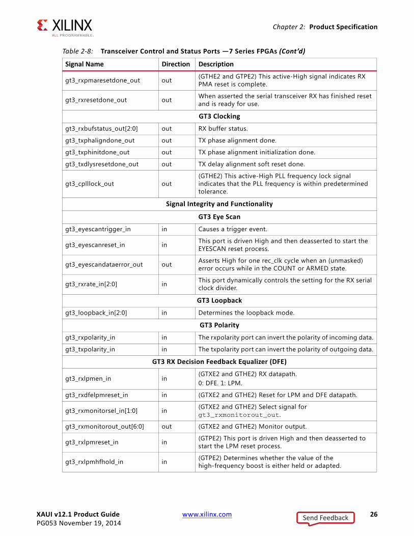
gt3_rxpmaresetdone_out out (GTHE2 and GTPE2) This active-High signal indicates RX PMA reset is complete.
gt3_rxresetdone_out out When asserted the serial transceiver RX has f inished reset and is ready for use.
GT3 Clocking
gt3_rxbufstatus_out[2:0] out RX buffer status.
gt3_txphaligndone_out out TX phase alignment done.
gt3_txphinitdone_out out TX phase alignment initialization done.
gt3_txdlysresetdone_out out TX delay alignment soft reset done.
gt3_cplllock_out out(GTHE2) This active-High PLL frequency lock signal indicates that the PLL frequency is within predetermined tolerance.
Signal Integrity and Functionality
GT3 Eye Scan
gt3_eyescantrigger_in in Causes a trigger event.
gt3_eyescanreset_in in This port is driven High and then deasserted to start the EYESCAN reset process.
gt3_eyescandataerror_out out Asserts High for one rec_clk cycle when an (unmasked) error occurs while in the COUNT or ARMED state.
gt3_rxrate_in[2:0] in This port dynamically controls the setting for the RX serial clock divider.
GT3 Loopback
gt3_loopback_in[2:0] in Determines the loopback mode.
GT3 Polarity
gt3_rxpolarity_in in The rxpolarity port can invert the polarity of incoming data.
gt3_txpolarity_in in The txpolarity port can invert the polarity of outgoing data.
GT3 RX Decision Feedback Equalizer (DFE)
gt3_rxlpmen_in in(GTXE2 and GTHE2) RX datapath. 0: DFE. 1: LPM.
gt3_rxdfelpmreset_in in (GTXE2 and GTHE2) Reset for LPM and DFE datapath.
gt3_rxmonitorsel_in[1:0] in (GTXE2 and GTHE2) Select signal for gt3_rxmonitorout_out.
gt3_rxmonitorout_out[6:0] out (GTXE2 and GTHE2) Monitor output.
gt3_rxlpmreset_in in (GTPE2) This port is driven High and then deasserted to start the LPM reset process.
gt3_rxlpmhfhold_in in (GTPE2) Determines whether the value of the high-frequency boost is either held or adapted.
Table 2-8: Transceiver Control and Status Ports —7 Series FPGAs (Cont’d)
Signal Name Direction Description
Send Feedback
XAUI v12.1 Product Guide www.xilinx.com 27PG053 November 19, 2014
Chapter 2: Product Specification
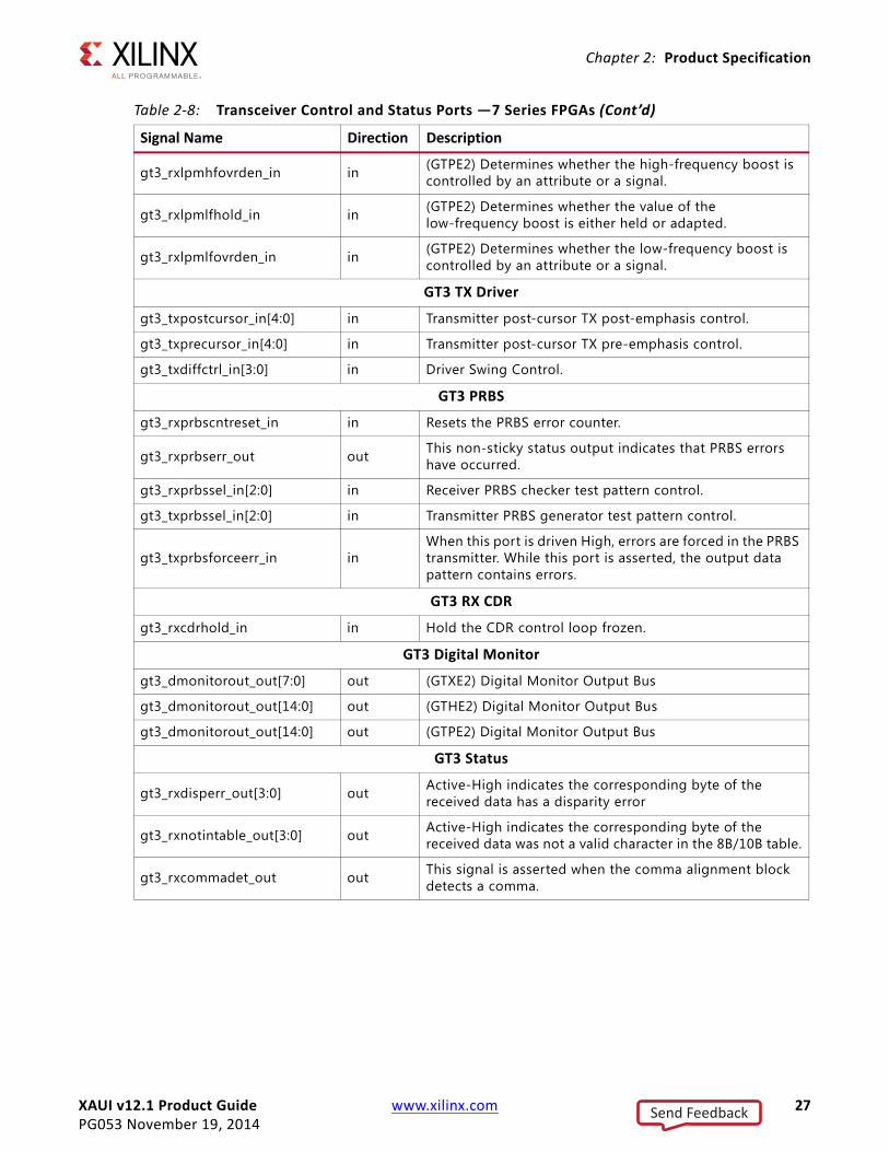
gt3_rxlpmhfovrden_in in (GTPE2) Determines whether the high-frequency boost is controlled by an attribute or a signal.
gt3_rxlpmlfhold_in in (GTPE2) Determines whether the value of the low-frequency boost is either held or adapted.
gt3_rxlpmlfovrden_in in (GTPE2) Determines whether the low-frequency boost is controlled by an attribute or a signal.
GT3 TX Driver
gt3_txpostcursor_in[4:0] in Transmitter post-cursor TX post-emphasis control.
gt3_txprecursor_in[4:0] in Transmitter post-cursor TX pre-emphasis control.
gt3_txdiffctrl_in[3:0] in Driver Swing Control.
GT3 PRBS
gt3_rxprbscntreset_in in Resets the PRBS error counter.
gt3_rxprbserr_out out This non-sticky status output indicates that PRBS errors have occurred.
gt3_rxprbssel_in[2:0] in Receiver PRBS checker test pattern control.
gt3_txprbssel_in[2:0] in Transmitter PRBS generator test pattern control.
gt3_txprbsforceerr_in inWhen this port is driven High, errors are forced in the PRBS transmitter. While this port is asserted, the output data pattern contains errors.
GT3 RX CDR
gt3_rxcdrhold_in in Hold the CDR control loop frozen.
GT3 Digital Monitor
gt3_dmonitorout_out[7:0] out (GTXE2) Digital Monitor Output Bus
gt3_dmonitorout_out[14:0] out (GTHE2) Digital Monitor Output Bus
gt3_dmonitorout_out[14:0] out (GTPE2) Digital Monitor Output Bus
GT3 Status
gt3_rxdisperr_out[3:0] out Active-High indicates the corresponding byte of the received data has a disparity error
gt3_rxnotintable_out[3:0] out Active-High indicates the corresponding byte of the received data was not a valid character in the 8B/10B table.
gt3_rxcommadet_out out This signal is asserted when the comma alignment block detects a comma.
Table 2-8: Transceiver Control and Status Ports —7 Series FPGAs (Cont’d)
Signal Name Direction Description
Send Feedback
XAUI v12.1 Product Guide www.xilinx.com 28PG053 November 19, 2014
Chapter 2: Product Specification
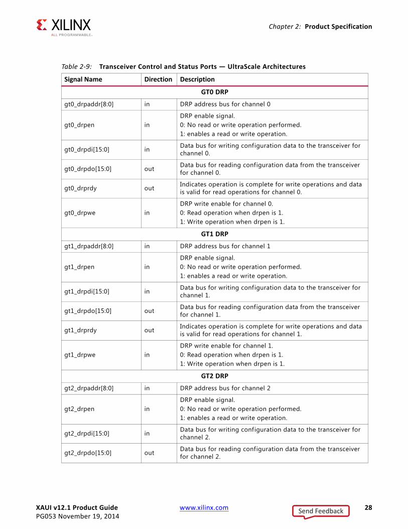
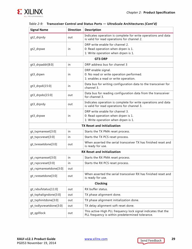
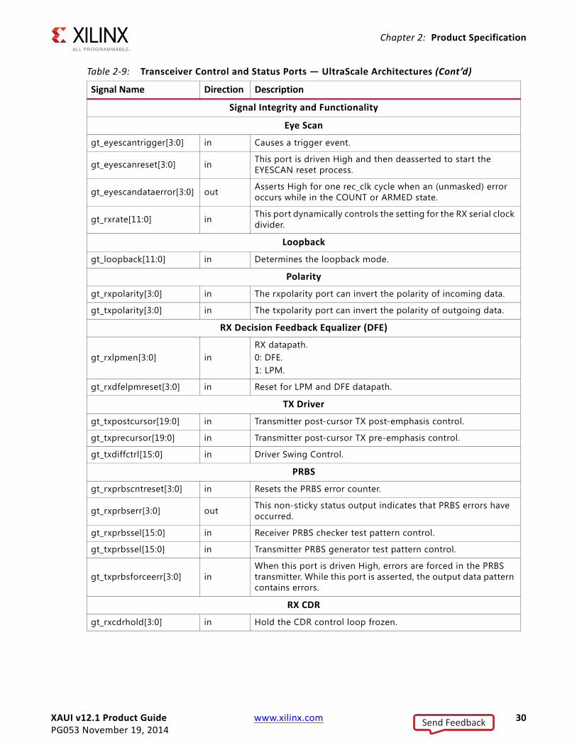
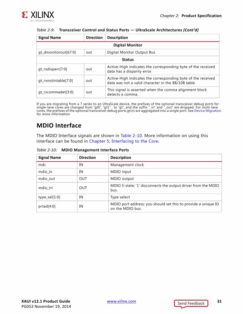
Table 2-9: Transceiver Control and Status Ports — UltraScale Architectures
Signal Name Direction Description
GT0 DRP
gt0_drpaddr[8:0] in DRP address bus for channel 0
gt0_drpen inDRP enable signal. 0: No read or write operation performed. 1: enables a read or write operation.
gt0_drpdi[15:0] in Data bus for writing configuration data to the transceiver for channel 0.
gt0_drpdo[15:0] out Data bus for reading configuration data from the transceiver for channel 0.
gt0_drprdy out Indicates operation is complete for write operations and data is valid for read operations for channel 0.
gt0_drpwe inDRP write enable for channel 0. 0: Read operation when drpen is 1. 1: Write operation when drpen is 1.
GT1 DRP
gt1_drpaddr[8:0] in DRP address bus for channel 1
gt1_drpen inDRP enable signal. 0: No read or write operation performed. 1: enables a read or write operation.
gt1_drpdi[15:0] in Data bus for writing configuration data to the transceiver for channel 1.
gt1_drpdo[15:0] out Data bus for reading configuration data from the transceiver for channel 1.
gt1_drprdy out Indicates operation is complete for write operations and data is valid for read operations for channel 1.
gt1_drpwe inDRP write enable for channel 1. 0: Read operation when drpen is 1. 1: Write operation when drpen is 1.
GT2 DRP
gt2_drpaddr[8:0] in DRP address bus for channel 2
gt2_drpen inDRP enable signal. 0: No read or write operation performed. 1: enables a read or write operation.
gt2_drpdi[15:0] in Data bus for writing configuration data to the transceiver for channel 2.
gt2_drpdo[15:0] out Data bus for reading configuration data from the transceiver for channel 2.
Send Feedback
XAUI v12.1 Product Guide www.xilinx.com 29PG053 November 19, 2014
Chapter 2: Product Specification
gt2_drprdy out Indicates operation is complete for write operations and data is valid for read operations for channel 2.
gt2_drpwe inDRP write enable for channel 2. 0: Read operation when drpen is 1. 1: Write operation when drpen is 1.
GT3 DRP
gt3_drpaddr[8:0] in DRP address bus for channel 3
gt3_drpen inDRP enable signal. 0: No read or write operation performed. 1: enables a read or write operation.
gt3_drpdi[15:0] in Data bus for writing configuration data to the transceiver for channel 3.
gt3_drpdo[15:0] out Data bus for reading configuration data from the transceiver for channel 3.
gt3_drprdy out Indicates operation is complete for write operations and data is valid for read operations for channel 3.
gt3_drpwe inDRP write enable for channel 3. 0: Read operation when drpen is 1. 1: Write operation when drpen is 1.
TX Reset and Initialization
gt_txpmareset[3:0] in Starts the TX PMA reset process.
gt_txpcsreset[3:0] in Starts the TX PCS reset process.
gt_txresetdone[3:0] out When asserted the serial transceiver TX has finished reset and is ready for use.
RX Reset and Initialization
gt_rxpmareset[3:0] in Starts the RX PMA reset process.
gt_rxpcsreset[3:0] in Starts the RX PCS reset process.
gt_rxpmaresetdone[3:0] out
gt_rxresetdone[3:0] out When asserted the serial transceiver RX has f inished reset and is ready for use.
Clocking
gt_rxbufstatus[11:0] out RX buffer status.
gt_txphaligndone[3:0] out TX phase alignment done.
gt_txphinitdone[3:0] out TX phase alignment initialization done.
gt_txdlysresetdone[3:0] out TX delay alignment soft reset done.
gt_qplllock out This active-High PLL frequency lock signal indicates that the PLL frequency is within predetermined tolerance.
Table 2-9: Transceiver Control and Status Ports — UltraScale Architectures (Cont’d)
Signal Name Direction Description
Send Feedback
XAUI v12.1 Product Guide www.xilinx.com 30PG053 November 19, 2014
Chapter 2: Product Specification
Signal Integrity and Functionality
Eye Scan
gt_eyescantrigger[3:0] in Causes a trigger event.
gt_eyescanreset[3:0] in This port is driven High and then deasserted to start the EYESCAN reset process.
gt_eyescandataerror[3:0] out Asserts High for one rec_clk cycle when an (unmasked) error occurs while in the COUNT or ARMED state.
gt_rxrate[11:0] in This port dynamically controls the setting for the RX serial clock divider.
Loopback
gt_loopback[11:0] in Determines the loopback mode.
Polarity
gt_rxpolarity[3:0] in The rxpolarity port can invert the polarity of incoming data.
gt_txpolarity[3:0] in The txpolarity port can invert the polarity of outgoing data.
RX Decision Feedback Equalizer (DFE)
gt_rxlpmen[3:0] inRX datapath. 0: DFE. 1: LPM.
gt_rxdfelpmreset[3:0] in Reset for LPM and DFE datapath.
TX Driver
gt_txpostcursor[19:0] in Transmitter post-cursor TX post-emphasis control.
gt_txprecursor[19:0] in Transmitter post-cursor TX pre-emphasis control.
gt_txdiffctrl[15:0] in Driver Swing Control.
PRBS
gt_rxprbscntreset[3:0] in Resets the PRBS error counter.
gt_rxprbserr[3:0] out This non-sticky status output indicates that PRBS errors have occurred.
gt_rxprbssel[15:0] in Receiver PRBS checker test pattern control.
gt_txprbssel[15:0] in Transmitter PRBS generator test pattern control.
gt_txprbsforceerr[3:0] inWhen this port is driven High, errors are forced in the PRBS transmitter. While this port is asserted, the output data pattern contains errors.
RX CDR
gt_rxcdrhold[3:0] in Hold the CDR control loop frozen.
Table 2-9: Transceiver Control and Status Ports — UltraScale Architectures (Cont’d)
Signal Name Direction Description
Send Feedback
XAUI v12.1 Product Guide www.xilinx.com 31PG053 November 19, 2014
Chapter 2: Product Specification
If you are migrating from a 7 series to an UltraScale device, the prefixes of the optional transceiver debug ports for single-lane cores are changed from “gt0”, “gt1” to “gt”, and the suff ix “_in” and “_out” are dropped. For multi-lane cores, the prefixes of the optional transceiver debug ports gt(n) are aggregated into a single port. See Device Migration for more information
MDIO InterfaceThe MDIO Interface signals are shown in Table 2-10. More information on using this interface can be found in Chapter 5, Interfacing to the Core.
Digital Monitor
gt_dmonitorout[67:0] out Digital Monitor Output Bus
Status
gt_rxdisperr[7:0] out Active-High indicates the corresponding byte of the received data has a disparity error.
gt_rxnotintable[7:0] out Active-High indicates the corresponding byte of the received data was not a valid character in the 8B/10B table.
gt_rxcommadet[3:0] out This signal is asserted when the comma alignment block detects a comma.
Table 2-10: MDIO Management Interface Ports
Signal Name Direction Description
mdc IN Management clock
mdio_in IN MDIO input
mdio_out OUT MDIO output
mdio_tri OUT MDIO 3-state; ‘1’ disconnects the output driver from the MDIO bus.
type_sel[1:0] IN Type select
prtad[4:0] IN MDIO port address; you should set this to provide a unique ID on the MDIO bus.
Table 2-9: Transceiver Control and Status Ports — UltraScale Architectures (Cont’d)
Signal Name Direction Description
Send Feedback
XAUI v12.1 Product Guide www.xilinx.com 32PG053 November 19, 2014
Chapter 2: Product Specification
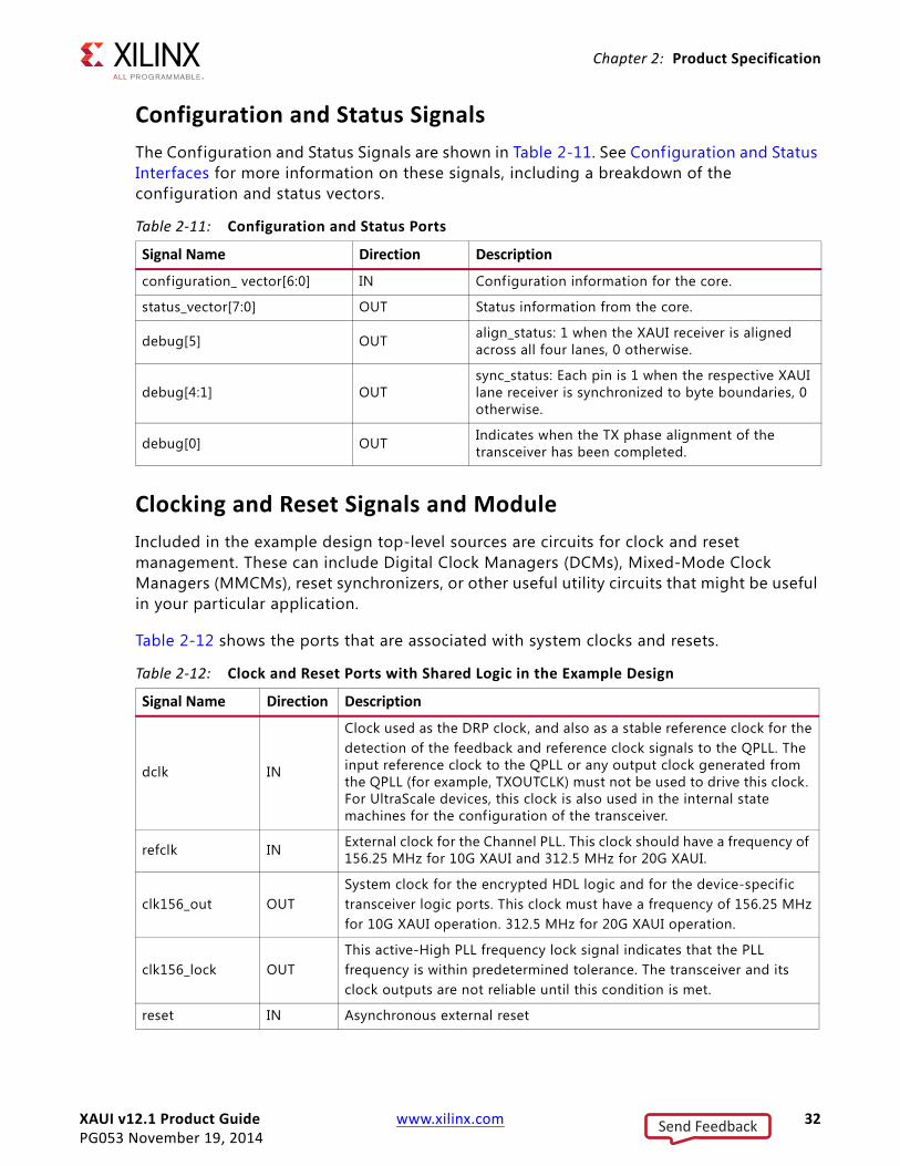
Configuration and Status SignalsThe Configuration and Status Signals are shown in Table 2-11. See Configuration and Status Interfaces for more information on these signals, including a breakdown of the configuration and status vectors.
Clocking and Reset Signals and ModuleIncluded in the example design top-level sources are circuits for clock and reset management. These can include Digital Clock Managers (DCMs), Mixed-Mode Clock Managers (MMCMs), reset synchronizers, or other useful utility circuits that might be useful in your particular application.
Table 2-12 shows the ports that are associated with system clocks and resets.
Table 2-11: Configuration and Status Ports
Signal Name Direction Description
configuration_ vector[6:0] IN Configuration information for the core.
status_vector[7:0] OUT Status information from the core.
debug[5] OUT align_status: 1 when the XAUI receiver is aligned across all four lanes, 0 otherwise.
debug[4:1] OUTsync_status: Each pin is 1 when the respective XAUI lane receiver is synchronized to byte boundaries, 0 otherwise.
debug[0] OUT Indicates when the TX phase alignment of the transceiver has been completed.
Table 2-12: Clock and Reset Ports with Shared Logic in the Example Design
Signal Name Direction Description
dclk IN
Clock used as the DRP clock, and also as a stable reference clock for thedetection of the feedback and reference clock signals to the QPLL. The input reference clock to the QPLL or any output clock generated from the QPLL (for example, TXOUTCLK) must not be used to drive this clock. For UltraScale devices, this clock is also used in the internal state machines for the configuration of the transceiver.
refclk IN External clock for the Channel PLL. This clock should have a frequency of 156.25 MHz for 10G XAUI and 312.5 MHz for 20G XAUI.
clk156_out OUTSystem clock for the encrypted HDL logic and for the device-specif ictransceiver logic ports. This clock must have a frequency of 156.25 MHzfor 10G XAUI operation. 312.5 MHz for 20G XAUI operation.
clk156_lock OUTThis active-High PLL frequency lock signal indicates that the PLLfrequency is within predetermined tolerance. The transceiver and itsclock outputs are not reliable until this condition is met.
reset IN Asynchronous external reset
Send Feedback
XAUI v12.1 Product Guide www.xilinx.com 33PG053 November 19, 2014
Chapter 2: Product Specification
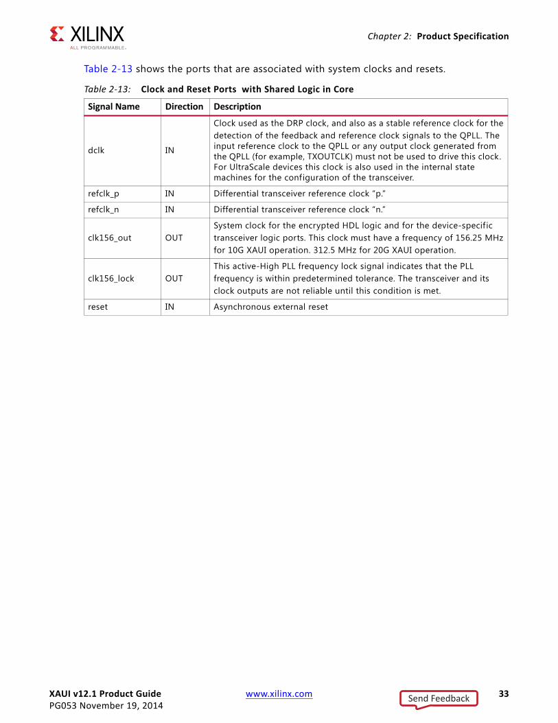
Table 2-13 shows the ports that are associated with system clocks and resets.
Table 2-13: Clock and Reset Ports with Shared Logic in Core
Signal Name Direction Description
dclk IN
Clock used as the DRP clock, and also as a stable reference clock for thedetection of the feedback and reference clock signals to the QPLL. The input reference clock to the QPLL or any output clock generated from the QPLL (for example, TXOUTCLK) must not be used to drive this clock. For UltraScale devices this clock is also used in the internal state machines for the configuration of the transceiver.
refclk_p IN Differential transceiver reference clock “p.”
refclk_n IN Differential transceiver reference clock “n.”
clk156_out OUTSystem clock for the encrypted HDL logic and for the device-specif ictransceiver logic ports. This clock must have a frequency of 156.25 MHzfor 10G XAUI operation. 312.5 MHz for 20G XAUI operation.
clk156_lock OUTThis active-High PLL frequency lock signal indicates that the PLLfrequency is within predetermined tolerance. The transceiver and itsclock outputs are not reliable until this condition is met.
reset IN Asynchronous external reset
Send Feedback
XAUI v12.1 Product Guide www.xilinx.com 34PG053 November 19, 2014
Chapter 2: Product Specification
Register Space
MDIO Management RegistersThe XAUI core, when generated with an MDIO interface, implements an MDIO Interface Register block. The core responds to MDIO transactions as either a 10GBASE-X PCS, a DTE XS, or a PHY XS depending on the setting of the type_sel port (see Table 2-10).
10GBASE-X PCS Registers
Table 2-14 shows the MDIO registers present when the XAUI core is configured as a 10GBASE-X PCS.
Table 2-14: 10GBASE-X PCS/PMA MDIO Registers
Register Address Register Name
1.0 Physical Medium Attachment/Physical Medium Dependent (PMA/PMD) Control 1
1.1 PMA/PMD Status 1
1.2,1.3 PMA/PMD Device Identif ier
1.4 PMA/PMD Speed Ability
1.5, 1.6 PMA/PMD Devices in Package
1.7 10G PMA/PMD Control 2
1.8 10G PMA/PMD Status 2
1.9 Reserved
1.10 10G PMD Receive Signal OK
1.11 to 1.13 Reserved
1.14, 1.15 PMA/PMD Package Identif ier
1.16 to 1.65 535 Reserved
3.0 PCS Control 1
3.1 PCS Status 1
3.2, 3.3 PCS Device Identif ier
3.4 PCS Speed Ability
3.5, 3.6 PCS Devices in Package
3.7 10G PCS Control 2
3.8 10G PCS Status 2
3.9 to 3.13 Reserved
3.14, 3.15 PCS Package Identif ier
3.16 to 3.23 Reserved
Send Feedback
XAUI v12.1 Product Guide www.xilinx.com 35PG053 November 19, 2014
Chapter 2: Product Specification
DTE XS Registers
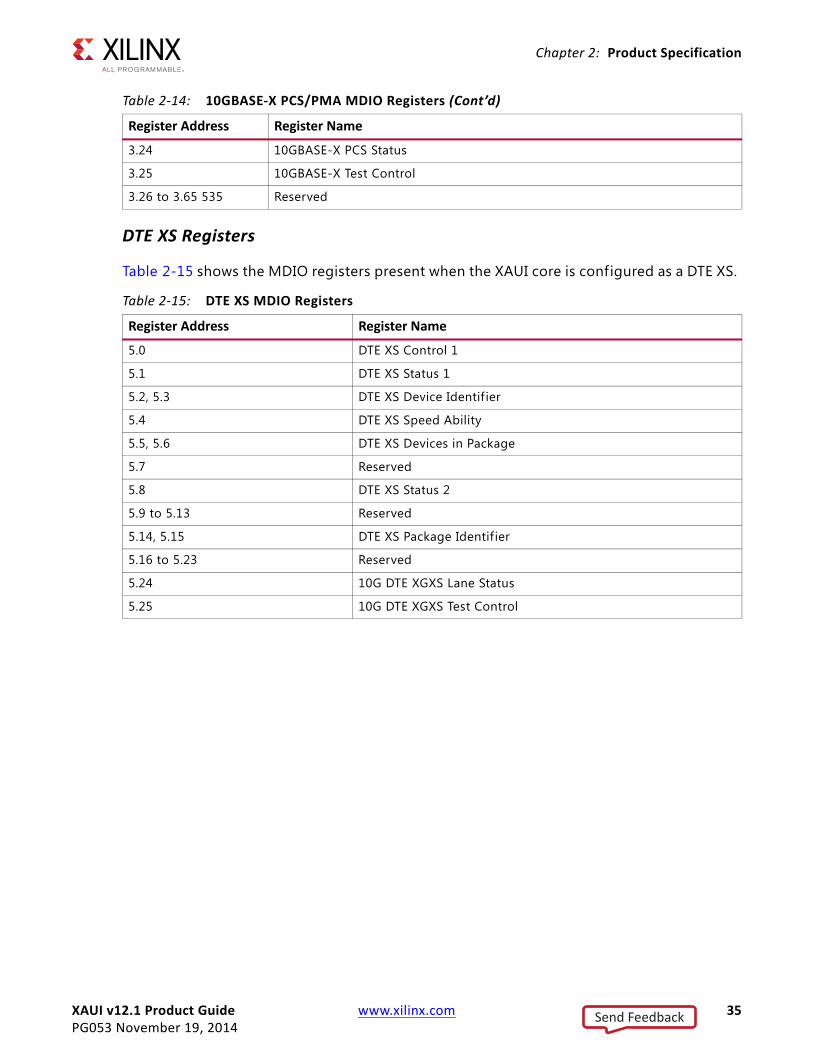
Table 2-15 shows the MDIO registers present when the XAUI core is configured as a DTE XS.
3.24 10GBASE-X PCS Status
3.25 10GBASE-X Test Control
3.26 to 3.65 535 Reserved
Table 2-15: DTE XS MDIO Registers
Register Address Register Name
5.0 DTE XS Control 1
5.1 DTE XS Status 1
5.2, 5.3 DTE XS Device Identif ier
5.4 DTE XS Speed Ability
5.5, 5.6 DTE XS Devices in Package
5.7 Reserved
5.8 DTE XS Status 2
5.9 to 5.13 Reserved
5.14, 5.15 DTE XS Package Identif ier
5.16 to 5.23 Reserved
5.24 10G DTE XGXS Lane Status
5.25 10G DTE XGXS Test Control
Table 2-14: 10GBASE-X PCS/PMA MDIO Registers (Cont’d)
Register Address Register Name
Send Feedback
XAUI v12.1 Product Guide www.xilinx.com 36PG053 November 19, 2014
Chapter 2: Product Specification
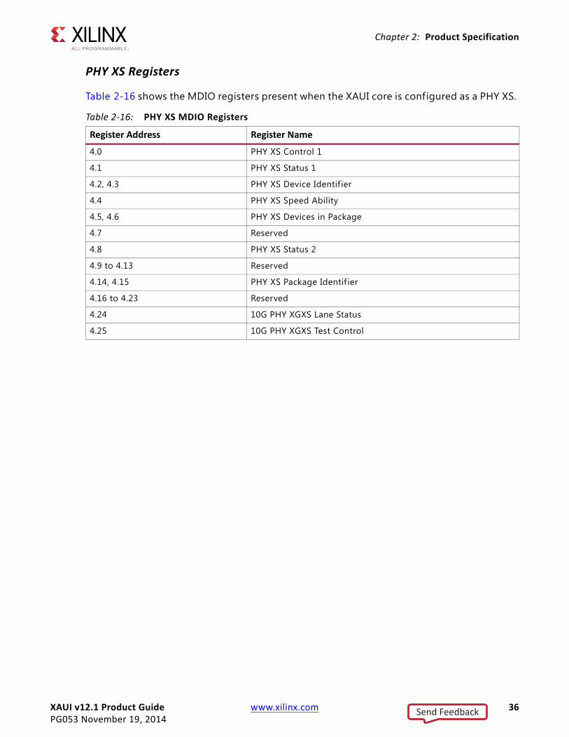
PHY XS Registers
Table 2-16 shows the MDIO registers present when the XAUI core is configured as a PHY XS.
Table 2-16: PHY XS MDIO Registers
Register Address Register Name
4.0 PHY XS Control 1
4.1 PHY XS Status 1
4.2, 4.3 PHY XS Device Identif ier
4.4 PHY XS Speed Ability
4.5, 4.6 PHY XS Devices in Package
4.7 Reserved
4.8 PHY XS Status 2
4.9 to 4.13 Reserved
4.14, 4.15 PHY XS Package Identif ier
4.16 to 4.23 Reserved
4.24 10G PHY XGXS Lane Status
4.25 10G PHY XGXS Test Control
Send Feedback
XAUI v12.1 Product Guide www.xilinx.com 37PG053 November 19, 2014
Chapter 3
Designing with the CoreThis chapter provides a general description of how to use the XAUI core in your designs and should be used in conjunction with Chapter 5, Interfacing to the Core which describes specific core interfaces.
This chapter also describes the steps required to turn a XAUI core into a fully-functioning design with user-application logic. It is important to realize that not all implementations require all of the design steps listed in this chapter. Follow the logic design guidelines in Chapter 6, Design Considerations.
Use the Example Design as a Starting PointEach instance of the XAUI core is delivered with an example design that can be implemented in an FPGA and simulated. This design can be used as a starting point for your own design or can be used to sanity-check your application in the event of diff iculty.
See Chapter 8, Detailed Example Design for information about using and customizing the example designs for the XAUI core.
Know the Degree of DifficultyXAUI designs are challenging to implement in any technology, and the degree of diff iculty is further influenced by:
• Maximum system clock frequency
• Targeted device architecture
• Nature of your application
All XAUI implementations need careful attention to system performance requirements. Pipelining, logic mapping, placement constraints, and logic duplication are all methods that help boost system performance.
Send Feedback
XAUI v12.1 Product Guide www.xilinx.com 38PG053 November 19, 2014
Chapter 3: Designing with the Core
Keep It RegisteredTo simplify timing and increase system performance in an FPGA design, keep all inputs and outputs registered between your application and the core. This means that all inputs and outputs from your application should come from, or connect to a flip-flop. While registering signals might not be possible for all paths, it simplif ies timing analysis and makes it easier for the Xilinx® tools to place and route the design.
Recognize Timing Critical SignalsThe supplied constraint f ile provided with the example design for the core identif ies the critical signals and the timing constraints that should be applied. See Chapter 8, Constraining the Core for further information.
Use Supported Design FlowsThe core HDL is added to the open Vivado® Design Suite project. Later the core is synthesized along with the rest of the project as part of project synthesis.
Make Only Allowed ModificationsThe XAUI core is not user-modif iable. Do not make modifications as they might have adverse effects on system timing and protocol compliance. Supported user configurations of the XAUI core can only be made by selecting the options from within the Vivado Design Suite when the core is generated. See Chapter 7, Customizing and Generating the Core.
Send Feedback
XAUI v12.1 Product Guide www.xilinx.com 39PG053 November 19, 2014
Chapter 4
Core ArchitectureThis chapter describes the overall architecture of the XAUI core and also describes the major interfaces to the core.
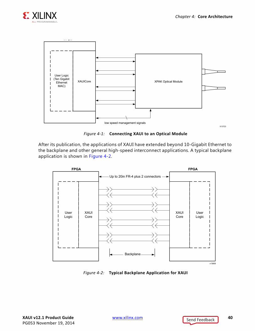
System OverviewXAUI is a four-lane, 3.125 Gb/s per-lane serial interface. 20 G – XAUI is supported in Zynq®-7000, Kintex®-7, Virtex®-7, and Artix®-7 devices (–2 speed grades) and UltraScale architecture using four transceivers at 6.25 Gb/s. Each lane is a differential pair, carrying current mode logic (CML) signaling; the data on each lane is 8B/10B encoded before transmission. Special code groups are used to allow each lane to synchronize at a word boundary and to deskew all four lanes into alignment at the receiving end. The XAUI standard is fully specif ied in clauses 47 and 48 of the 10-Gigabit Ethernet specif ication IEEE Std. 802.3-2012.
The XAUI standard was initially developed as a means to extend the physical separation possible between Media Access Controller (MAC) and physical-side interface (PHY) components in a 10-Gigabit Ethernet system distributed across a circuit board, and to reduce the number of interface signals in comparison with the Ten Gigabit Ethernet Media Independent Interface (XGMII). Figure 4-1 shows the XAUI core being used to connect to a 10-Gigabit Expansion Pack (XPAK) optical module.
Send Feedback
XAUI v12.1 Product Guide www.xilinx.com 40PG053 November 19, 2014
Chapter 4: Core Architecture
After its publication, the applications of XAUI have extended beyond 10-Gigabit Ethernet to the backplane and other general high-speed interconnect applications. A typical backplane application is shown in Figure 4-2.
X-Ref Target - Figure 4-1
Figure 4-1: Connecting XAUI to an Optical Module
X-Ref Target - Figure 4-2
Figure 4-2: Typical Backplane Application for XAUI
Send Feedback
XAUI v12.1 Product Guide www.xilinx.com 41PG053 November 19, 2014
Chapter 4: Core Architecture
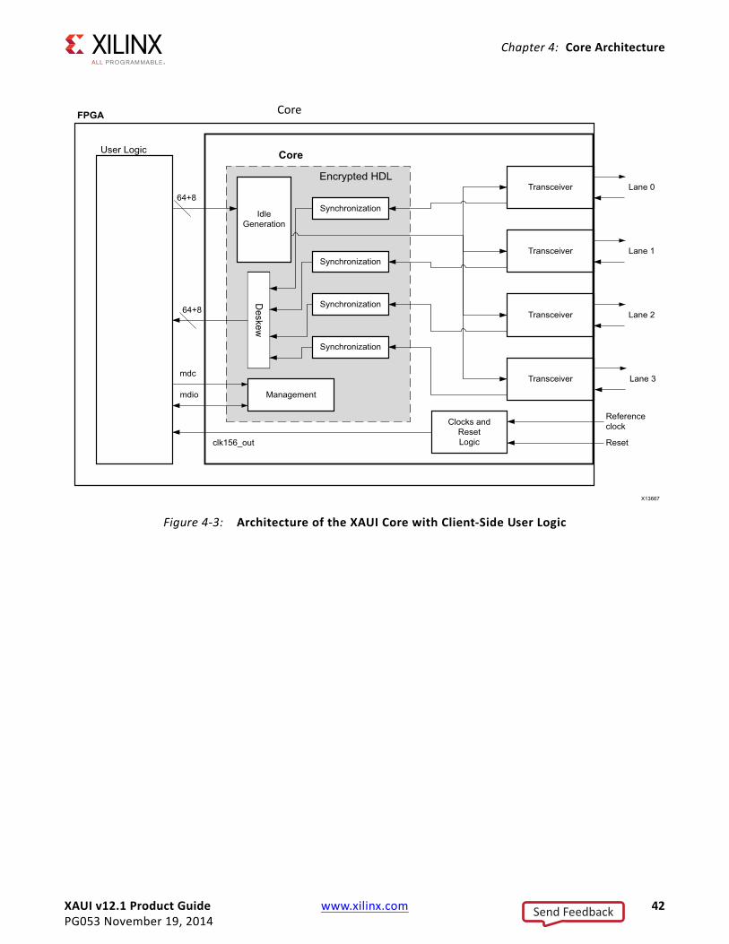
Functional DescriptionFigure 4-3 shows a block diagram of the implementation of the XAUI core. The architecture is similar for all supported devices. The major functional blocks of the core include the following:
• Transmit idle generation logic
Creates the code groups to allow synchronization and alignment at the receiver.
• Synchronization state machine (one per lane)
Identif ies byte boundaries in incoming serial data.
• Deskew state machine
Deskews the four received lanes into alignment.
• Optional MDIO interface
A 2-wire low-speed serial interface used to manage the core.
• Embedded FPGA transceivers. Provides high-speed transceivers as well as 8B/10B encode and decode, and elastic buffering in the receive datapath.
Send Feedback
XAUI v12.1 Product Guide www.xilinx.com 42PG053 November 19, 2014
Chapter 4: Core Architecture
X-Ref Target - Figure 4-3
Figure 4-3: Architecture of the XAUI Core with Client-Side User Logic
Send Feedback
XAUI v12.1 Product Guide www.xilinx.com 43PG053 November 19, 2014
Chapter 5
Interfacing to the CoreThis chapter describes how to connect to the data interfaces of the core and configuration and status interfaces of the XAUI core.
Data Interface: Internal XGMII Interfaces
Internal 64-bit SDR Client-side InterfaceThe 64-bit single-data rate (SDR) client-side interface is based upon a 32-bit XGMII-like interface. The key difference is a demultiplexing of the bus from 32- bits wide to 64-bits wide on a single rising clock edge. This demultiplexing is done by extending the bus upwards so that there are now eight lanes of data numbered 0–7; the lanes are organized such that data appearing on lanes 4–7 is transmitted or received later in time than that in lanes 0–3.
The mapping of lanes to data bits is shown in Table 5-1. The lane number is also the index of the control bit for that particular lane; for example, xgmii_txc[2] and xgmii_txd[23:16] are the control and data bits respectively for lane 2.
Table 5-1: xgmii_txd, xgmii_rxd Lanes for Internal 64-bit Client-Side Interface
Lane xgmii_txd, xgmii_rxd Bits
0 7:0
1 15:8
2 23:16
3 31:24
4 39:32
5 47:40
6 55:48
7 63:56
Send Feedback
XAUI v12.1 Product Guide www.xilinx.com 44PG053 November 19, 2014
Chapter 5: Interfacing to the Core
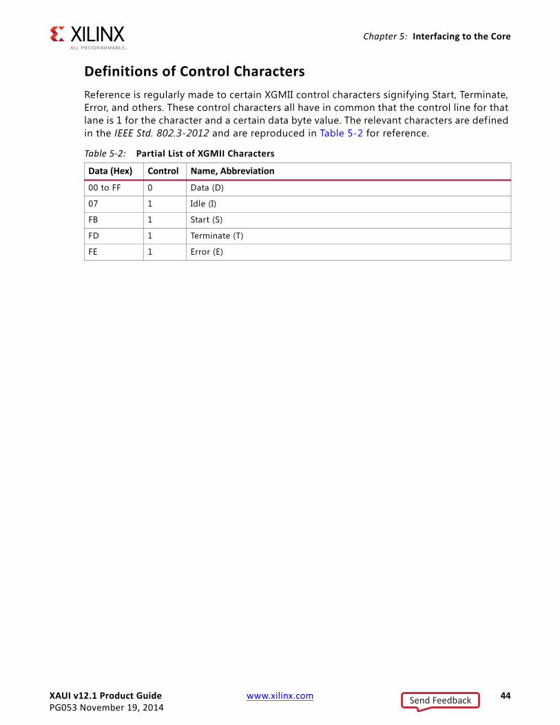
Definitions of Control CharactersReference is regularly made to certain XGMII control characters signifying Start, Terminate, Error, and others. These control characters all have in common that the control line for that lane is 1 for the character and a certain data byte value. The relevant characters are defined in the IEEE Std. 802.3-2012 and are reproduced in Table 5-2 for reference.
Table 5-2: Partial List of XGMII Characters
Data (Hex) Control Name, Abbreviation
00 to FF 0 Data (D)
07 1 Idle (I)
FB 1 Start (S)
FD 1 Terminate (T)
FE 1 Error (E)
Send Feedback
XAUI v12.1 Product Guide www.xilinx.com 45PG053 November 19, 2014
Chapter 5: Interfacing to the Core
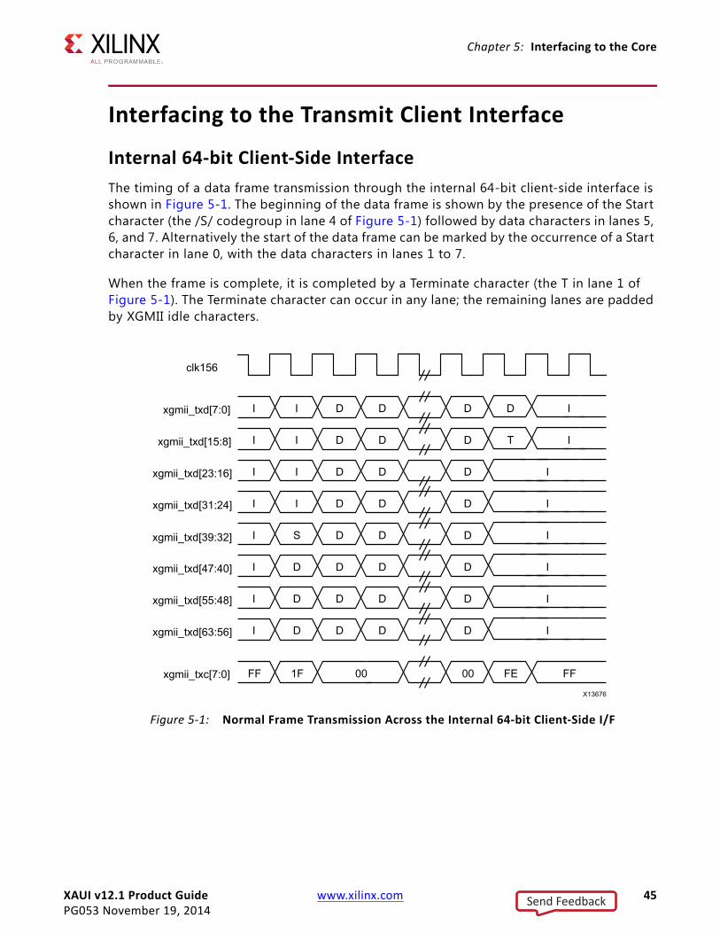
Interfacing to the Transmit Client Interface
Internal 64-bit Client-Side InterfaceThe timing of a data frame transmission through the internal 64-bit client-side interface is shown in Figure 5-1. The beginning of the data frame is shown by the presence of the Start character (the /S/ codegroup in lane 4 of Figure 5-1) followed by data characters in lanes 5, 6, and 7. Alternatively the start of the data frame can be marked by the occurrence of a Start character in lane 0, with the data characters in lanes 1 to 7.
When the frame is complete, it is completed by a Terminate character (the T in lane 1 of Figure 5-1). The Terminate character can occur in any lane; the remaining lanes are padded by XGMII idle characters.X-Ref Target - Figure 5-1
Figure 5-1: Normal Frame Transmission Across the Internal 64-bit Client-Side I/F
Send Feedback
XAUI v12.1 Product Guide www.xilinx.com 46PG053 November 19, 2014
Chapter 5: Interfacing to the Core
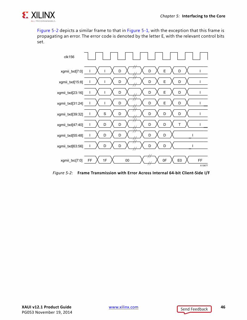
Figure 5-2 depicts a similar frame to that in Figure 5-1, with the exception that this frame is propagating an error. The error code is denoted by the letter E, with the relevant control bits set.X-Ref Target - Figure 5-2
Figure 5-2: Frame Transmission with Error Across Internal 64-bit Client-Side I/F
Send Feedback
XAUI v12.1 Product Guide www.xilinx.com 47PG053 November 19, 2014
Chapter 5: Interfacing to the Core
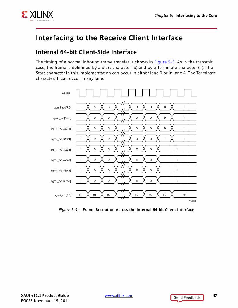
Interfacing to the Receive Client Interface
Internal 64-bit Client-Side InterfaceThe timing of a normal inbound frame transfer is shown in Figure 5-3. As in the transmit case, the frame is delimited by a Start character (S) and by a Terminate character (T). The Start character in this implementation can occur in either lane 0 or in lane 4. The Terminate character, T, can occur in any lane.X-Ref Target - Figure 5-3
Figure 5-3: Frame Reception Across the Internal 64-bit Client Interface
Send Feedback
XAUI v12.1 Product Guide www.xilinx.com 48PG053 November 19, 2014
Chapter 5: Interfacing to the Core
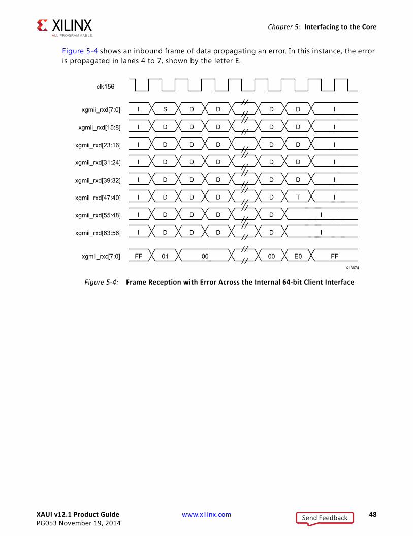
Figure 5-4 shows an inbound frame of data propagating an error. In this instance, the error is propagated in lanes 4 to 7, shown by the letter E.X-Ref Target - Figure 5-4
Figure 5-4: Frame Reception with Error Across the Internal 64-bit Client Interface
Send Feedback
XAUI v12.1 Product Guide www.xilinx.com 49PG053 November 19, 2014
Chapter 5: Interfacing to the Core
Configuration and Status InterfacesThis section describes the interfaces available for dynamically setting the configuration and obtaining the status of the XAUI core. There are two interfaces for configuration; depending on the core customization, only one is available in a particular core instance. The interfaces are:
• MDIO Interface
• Configuration and Status Vectors
In addition, there are output ports on the core signaling alignment and synchronization status. These ports are described in Debug Port.
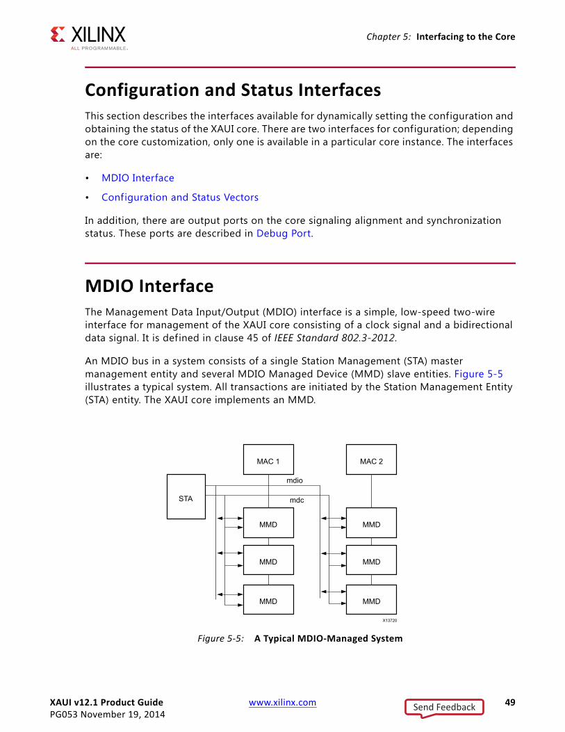
MDIO InterfaceThe Management Data Input/Output (MDIO) interface is a simple, low-speed two-wire interface for management of the XAUI core consisting of a clock signal and a bidirectional data signal. It is defined in clause 45 of IEEE Standard 802.3-2012.
An MDIO bus in a system consists of a single Station Management (STA) master management entity and several MDIO Managed Device (MMD) slave entities. Figure 5-5 illustrates a typical system. All transactions are initiated by the Station Management Entity (STA) entity. The XAUI core implements an MMD.
X-Ref Target - Figure 5-5
Figure 5-5: A Typical MDIO-Managed System
Send Feedback
XAUI v12.1 Product Guide www.xilinx.com 50PG053 November 19, 2014
Chapter 5: Interfacing to the Core
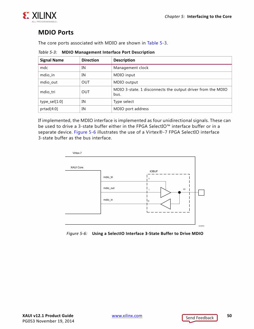
MDIO PortsThe core ports associated with MDIO are shown in Table 5-3.
If implemented, the MDIO interface is implemented as four unidirectional signals. These can be used to drive a 3-state buffer either in the FPGA SelectIO™ interface buffer or in a separate device. Figure 5-6 illustrates the use of a Virtex®-7 FPGA SelectIO interface 3-state buffer as the bus interface.
Table 5-3: MDIO Management Interface Port Description
Signal Name Direction Description
mdc IN Management clock
mdio_in IN MDIO input
mdio_out OUT MDIO output
mdio_tri OUT MDIO 3-state. 1 disconnects the output driver from the MDIO bus.
type_sel[1:0] IN Type select
prtad[4:0] IN MDIO port address
X-Ref Target - Figure 5-6
Figure 5-6: Using a SelectIO Interface 3-State Buffer to Drive MDIO
Send Feedback
XAUI v12.1 Product Guide www.xilinx.com 51PG053 November 19, 2014
Chapter 5: Interfacing to the Core
The type_sel port is registered into the core at FPGA configuration and core hard reset; changes after that time are ignored by the core. Table 5-4 shows the mapping of the type_sel setting to the implemented register map.
The prtad[4:0] port sets the port address of the core instance. Multiple instances of the same core can be supported on the same MDIO bus by setting prtad[4:0] to a unique value for each instance; the XAUI core ignores transactions with the PRTAD field set to a value other than that on its prtad[4:0] port.
MDIO TransactionsThe MDIO interface should be driven from a STA master according to the protocol defined in IEEE Std. 802.3-2012. An outline of each transaction type is described in the following sections. In these sections, the following abbreviations apply:
• PRE: preamble
• ST: start
• OP: operation code
• PRTAD: port address
• DEVAD: device address
• TA: turnaround
Table 5-4: Mapping of type_sel Port Settings to MDIO Register Type
type_sel setting MDIO Register Description
00 or 01 10GBASE-X PCS/PMA When driving a 10GBASE-X PHY
10
Data Terminal Equipment (DTE) XGMII Extender Sublayer (XGXS)
When connected to a 10GMAC through XGMII
11 PHY XGXS When connected to a PHY through XGMII
Send Feedback
XAUI v12.1 Product Guide www.xilinx.com 52PG053 November 19, 2014
Chapter 5: Interfacing to the Core
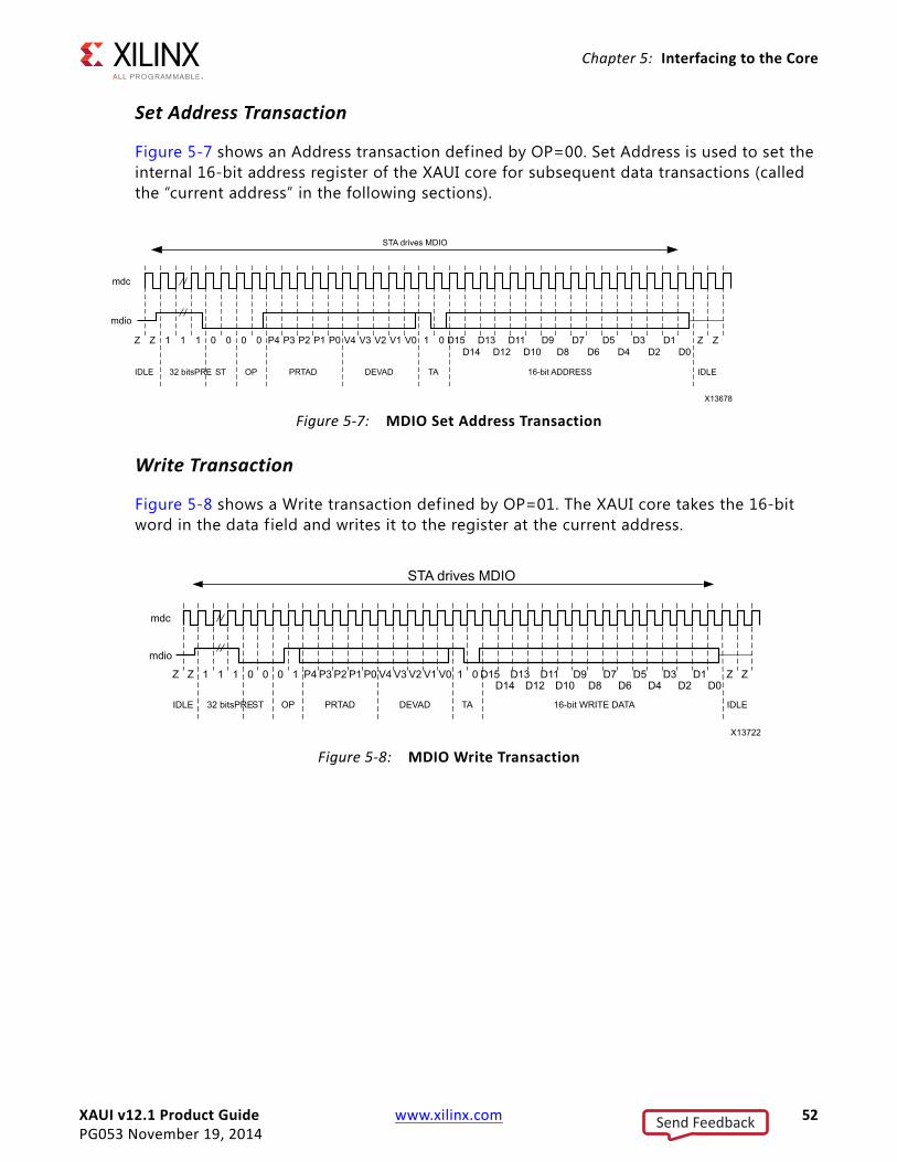
Set Address Transaction
Figure 5-7 shows an Address transaction defined by OP=00. Set Address is used to set the internal 16-bit address register of the XAUI core for subsequent data transactions (called the “current address” in the following sections).
Write Transaction
Figure 5-8 shows a Write transaction defined by OP=01. The XAUI core takes the 16-bit word in the data f ield and writes it to the register at the current address.
X-Ref Target - Figure 5-7
Figure 5-7: MDIO Set Address Transaction
X-Ref Target - Figure 5-8
Figure 5-8: MDIO Write Transaction
Send Feedback
XAUI v12.1 Product Guide www.xilinx.com 53PG053 November 19, 2014
Chapter 5: Interfacing to the Core
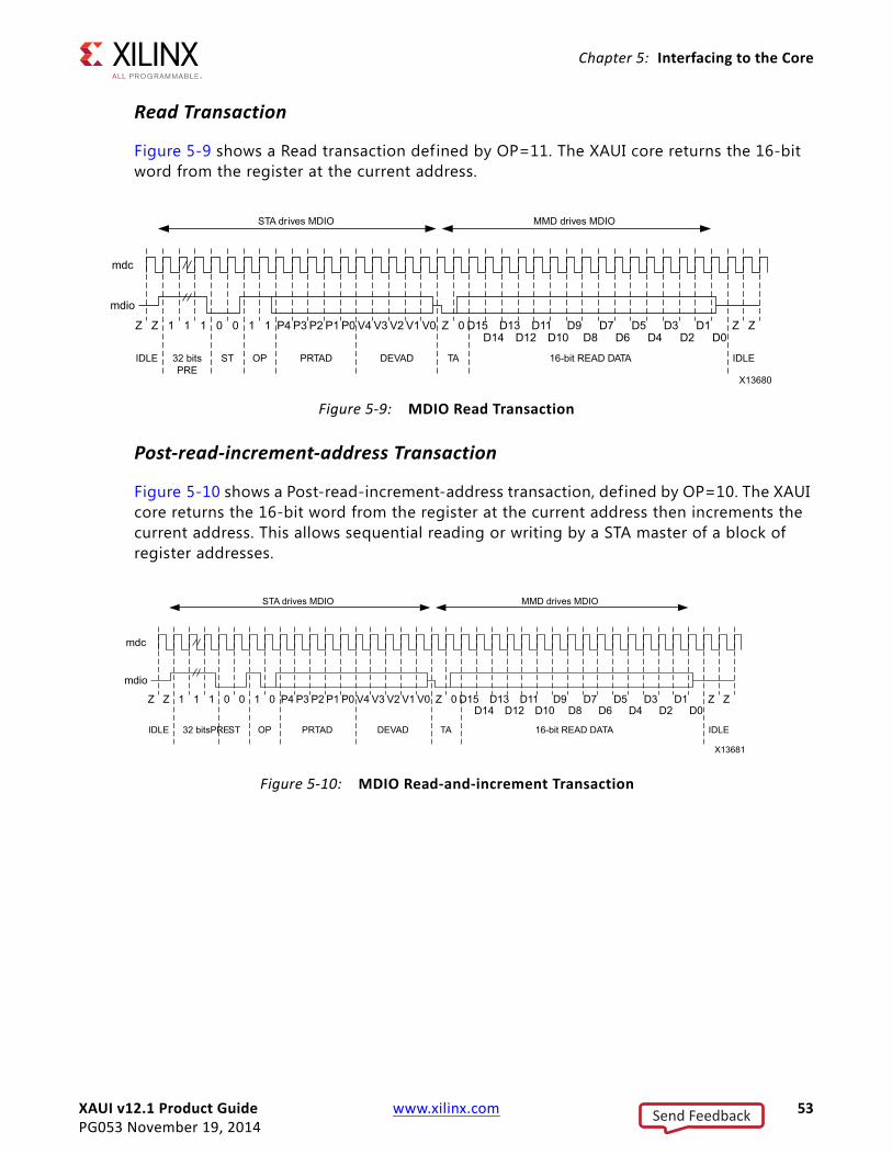
Read Transaction
Figure 5-9 shows a Read transaction defined by OP=11. The XAUI core returns the 16-bit word from the register at the current address.
Post-read-increment-address Transaction
Figure 5-10 shows a Post-read-increment-address transaction, defined by OP=10. The XAUI core returns the 16-bit word from the register at the current address then increments the current address. This allows sequential reading or writing by a STA master of a block of register addresses.
X-Ref Target - Figure 5-9
Figure 5-9: MDIO Read Transaction
X-Ref Target - Figure 5-10
Figure 5-10: MDIO Read-and-increment Transaction
Send Feedback
XAUI v12.1 Product Guide www.xilinx.com 54PG053 November 19, 2014
Chapter 5: Interfacing to the Core
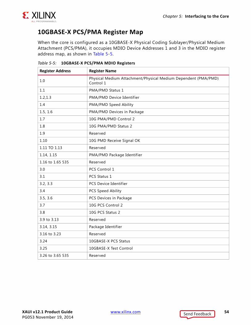
10GBASE-X PCS/PMA Register MapWhen the core is configured as a 10GBASE-X Physical Coding Sublayer/Physical Medium Attachment (PCS/PMA), it occupies MDIO Device Addresses 1 and 3 in the MDIO register address map, as shown in Table 5-5.
Table 5-5: 10GBASE-X PCS/PMA MDIO Registers
Register Address Register Name
1.0 Physical Medium Attachment/Physical Medium Dependent (PMA/PMD) Control 1
1.1 PMA/PMD Status 1
1.2,1.3 PMA/PMD Device Identif ier
1.4 PMA/PMD Speed Ability
1.5, 1.6 PMA/PMD Devices in Package
1.7 10G PMA/PMD Control 2
1.8 10G PMA/PMD Status 2
1.9 Reserved
1.10 10G PMD Receive Signal OK
1.11 TO 1.13 Reserved
1.14, 1.15 PMA/PMD Package Identif ier
1.16 to 1.65 535 Reserved
3.0 PCS Control 1
3.1 PCS Status 1
3.2, 3.3 PCS Device Identif ier
3.4 PCS Speed Ability
3.5, 3.6 PCS Devices in Package
3.7 10G PCS Control 2
3.8 10G PCS Status 2
3.9 to 3.13 Reserved
3.14, 3.15 Package Identif ier
3.16 to 3.23 Reserved
3.24 10GBASE-X PCS Status
3.25 10GBASE-X Test Control
3.26 to 3.65 535 Reserved
Send Feedback
XAUI v12.1 Product Guide www.xilinx.com 55PG053 November 19, 2014
Chapter 5: Interfacing to the Core
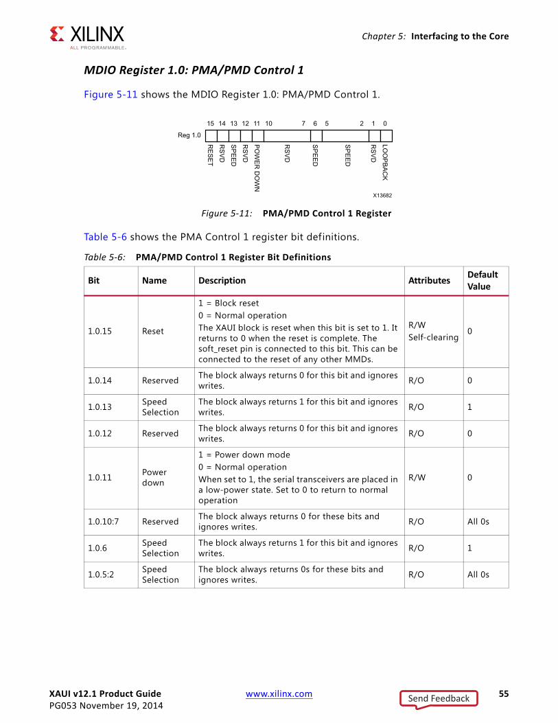
MDIO Register 1.0: PMA/PMD Control 1
Figure 5-11 shows the MDIO Register 1.0: PMA/PMD Control 1.
Table 5-6 shows the PMA Control 1 register bit definitions.
X-Ref Target - Figure 5-11
Figure 5-11: PMA/PMD Control 1 Register
Table 5-6: PMA/PMD Control 1 Register Bit Definitions
Bit Name Description Attributes Default Value
1.0.15 Reset
1 = Block reset0 = Normal operationThe XAUI block is reset when this bit is set to 1. It returns to 0 when the reset is complete. The soft_reset pin is connected to this bit. This can be connected to the reset of any other MMDs.
R/WSelf-clearing
0
1.0.14 Reserved The block always returns 0 for this bit and ignores writes. R/O 0
1.0.13 Speed Selection
The block always returns 1 for this bit and ignores writes. R/O 1
1.0.12 Reserved The block always returns 0 for this bit and ignores writes. R/O 0
1.0.11 Power down
1 = Power down mode0 = Normal operationWhen set to 1, the serial transceivers are placed in a low-power state. Set to 0 to return to normal operation
R/W 0
1.0.10:7 Reserved The block always returns 0 for these bits and ignores writes. R/O All 0s
1.0.6 Speed Selection
The block always returns 1 for this bit and ignores writes. R/O 1
1.0.5:2 Speed Selection
The block always returns 0s for these bits and ignores writes. R/O All 0s
Send Feedback
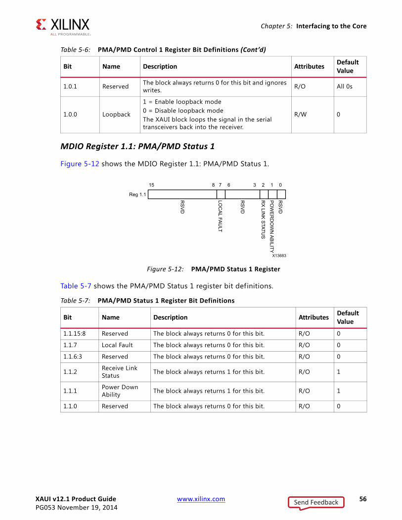
XAUI v12.1 Product Guide www.xilinx.com 56PG053 November 19, 2014
Chapter 5: Interfacing to the Core
MDIO Register 1.1: PMA/PMD Status 1
Figure 5-12 shows the MDIO Register 1.1: PMA/PMD Status 1.
Table 5-7 shows the PMA/PMD Status 1 register bit definitions.
1.0.1 Reserved The block always returns 0 for this bit and ignores writes. R/O All 0s
1.0.0 Loopback
1 = Enable loopback mode0 = Disable loopback modeThe XAUI block loops the signal in the serial transceivers back into the receiver.
R/W 0
X-Ref Target - Figure 5-12
Figure 5-12: PMA/PMD Status 1 Register
Table 5-7: PMA/PMD Status 1 Register Bit Definitions
Bit Name Description Attributes Default Value
1.1.15:8 Reserved The block always returns 0 for this bit. R/O 0
1.1.7 Local Fault The block always returns 0 for this bit. R/O 0
1.1.6:3 Reserved The block always returns 0 for this bit. R/O 0
1.1.2 Receive Link Status The block always returns 1 for this bit. R/O 1
1.1.1 Power Down Ability The block always returns 1 for this bit. R/O 1
1.1.0 Reserved The block always returns 0 for this bit. R/O 0
Table 5-6: PMA/PMD Control 1 Register Bit Definitions (Cont’d)
Bit Name Description Attributes Default Value
Send Feedback
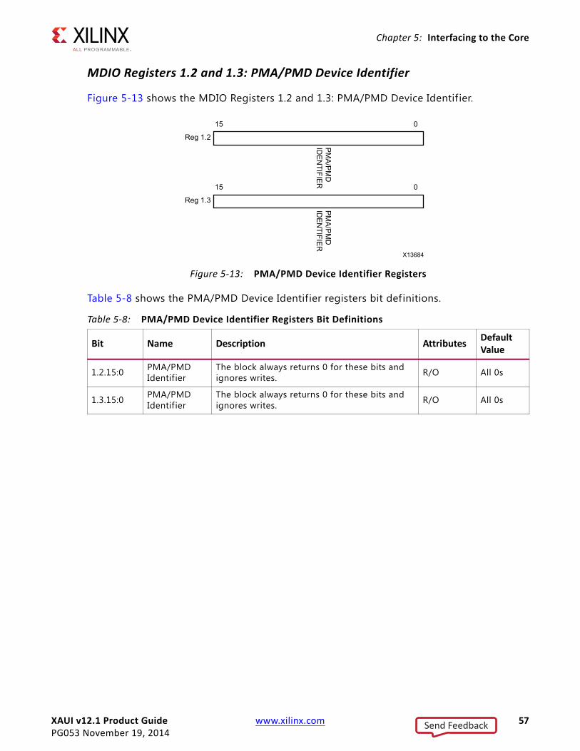
XAUI v12.1 Product Guide www.xilinx.com 57PG053 November 19, 2014
Chapter 5: Interfacing to the Core
MDIO Registers 1.2 and 1.3: PMA/PMD Device Identifier
Figure 5-13 shows the MDIO Registers 1.2 and 1.3: PMA/PMD Device Identif ier.
Table 5-8 shows the PMA/PMD Device Identif ier registers bit definitions.
X-Ref Target - Figure 5-13
Figure 5-13: PMA/PMD Device Identifier Registers
Table 5-8: PMA/PMD Device Identifier Registers Bit Definitions
Bit Name Description Attributes Default Value
1.2.15:0 PMA/PMD Identif ier
The block always returns 0 for these bits and ignores writes. R/O All 0s
1.3.15:0 PMA/PMD Identif ier
The block always returns 0 for these bits and ignores writes. R/O All 0s
Send Feedback
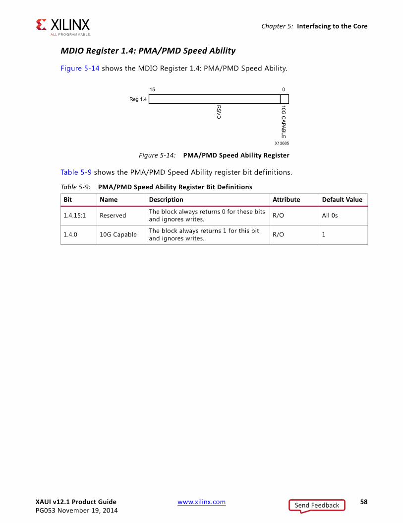
XAUI v12.1 Product Guide www.xilinx.com 58PG053 November 19, 2014
Chapter 5: Interfacing to the Core
MDIO Register 1.4: PMA/PMD Speed Ability
Figure 5-14 shows the MDIO Register 1.4: PMA/PMD Speed Ability.
Table 5-9 shows the PMA/PMD Speed Ability register bit definitions.
X-Ref Target - Figure 5-14
Figure 5-14: PMA/PMD Speed Ability Register
Table 5-9: PMA/PMD Speed Ability Register Bit Definitions
Bit Name Description Attribute Default Value
1.4.15:1 Reserved The block always returns 0 for these bits and ignores writes. R/O All 0s
1.4.0 10G Capable The block always returns 1 for this bit and ignores writes. R/O 1
Send Feedback
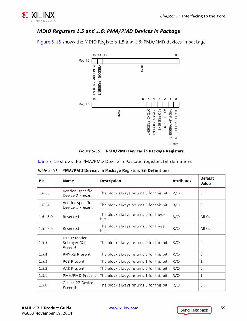
XAUI v12.1 Product Guide www.xilinx.com 59PG053 November 19, 2014
Chapter 5: Interfacing to the Core
MDIO Registers 1.5 and 1.6: PMA/PMD Devices in Package
Figure 5-15 shows the MDIO Registers 1.5 and 1.6: PMA/PMD devices in package.
Table 5-10 shows the PMA/PMD Device in Package registers bit definitions.
X-Ref Target - Figure 5-15
Figure 5-15: PMA/PMD Devices in Package Registers
Table 5-10: PMA/PMD Devices in Package Registers Bit Definitions
Bit Name Description Attributes Default Value
1.6.15 Vendor- specif ic Device 2 Present The block always returns 0 for this bit. R/O 0
1.6.14 Vendor-specif ic Device 1 Present The block always returns 0 for this bit. R/O 0
1.6.13:0 Reserved The block always returns 0 for these bits. R/O All 0s
1.5.15:6 Reserved The block always returns 0 for these bits. R/O All 0s
1.5.5DTE Extender Sublayer (XS) Present
The block always returns 0 for this bit. R/O 0
1.5.4 PHY XS Present The block always returns 0 for this bit. R/O 0
1.5.3 PCS Present The block always returns 1 for this bit. R/O 1
1.5.2 WIS Present The block always returns 0 for this bit. R/O 0
1.5.1 PMA/PMD Present The block always returns 1 for this bit. R/O 1
1.5.0 Clause 22 Device Present The block always returns 0 for this bit. R/O 0
Send Feedback
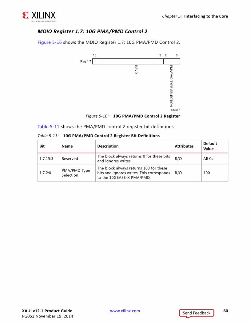
XAUI v12.1 Product Guide www.xilinx.com 60PG053 November 19, 2014
Chapter 5: Interfacing to the Core
MDIO Register 1.7: 10G PMA/PMD Control 2
Figure 5-16 shows the MDIO Register 1.7: 10G PMA/PMD Control 2.
Table 5-11 shows the PMA/PMD control 2 register bit definitions.
X-Ref Target - Figure 5-16
Figure 5-16: 10G PMA/PMD Control 2 Register
Table 5-11: 10G PMA/PMD Control 2 Register Bit Definitions
Bit Name Description Attributes Default Value
1.7.15:3 Reserved The block always returns 0 for these bits and ignores writes. R/O All 0s
1.7.2:0 PMA/PMD Type Selection
The block always returns 100 for these bits and ignores writes. This corresponds to the 10GBASE-X PMA/PMD.
R/O 100
Send Feedback
XAUI v12.1 Product Guide www.xilinx.com 61PG053 November 19, 2014
Chapter 5: Interfacing to the Core
MDIO Register 1.8: 10G PMA/PMD Status 2
Figure 5-17 shows the MDIO Register 1.8: 10G PMA/PMD Status 2.
Table 5-12 shows the PMA/PMD status 2 register bit definitions.
X-Ref Target - Figure 5-17
Figure 5-17: 10G PMA/PMD Status 2 Register
Table 5-12: 10G PMA/PMD Status 2 Register Bit Definitions
Bit Name Description Attributes Default Value
1.8.15:14 Device Present The block always returns 10 for these bits. R/O 10
1.8.13 Transmit Local Fault Ability
The block always returns 0 for this bit. R/O 0
1.8.12 Receive Local Fault Ability
The block always returns 0 for this bit. R/O 0
1.8.11 Transmit Fault The block always returns 0 for this bit. R/O 0
1.8.10 Receive Fault The block always returns 0 for this bit. R/O 0
1.8.9 Reserved The block always returns 0 for this bit. R/O 0
1.8.8 PMD Transmit Disable Ability
The block always returns 0 for this bit. R/O 0
1.8.7 10GBASE-SR Ability
The block always returns 0 for this bit. R/O 0
1.8.6 10GBASE-LR Ability
The block always returns 0 for this bit. R/O 0
1.8.5 10GBASE-ER Ability
The block always returns 0 for this bit. R/O 0
1.8.4 10GBASE-LX4 Ability
The block always returns 1 for this bit. R/O 1
1.8.3 10GBASE-SW Ability
The block always returns 0 for this bit. R/O 0
Send Feedback
XAUI v12.1 Product Guide www.xilinx.com 62PG053 November 19, 2014
Chapter 5: Interfacing to the Core
1.8.2 10GBASE-LW Ability
The block always returns 0 for this bit. R/O 0
1.8.1 10GBASE-EW Ability
The block always returns 0 for this bit. R/O 0
1.8.0 PMA Loopback Ability
The block always returns 1 for this bit. R/O 1
Table 5-12: 10G PMA/PMD Status 2 Register Bit Definitions (Cont’d)
Bit Name Description Attributes Default Value
Send Feedback
XAUI v12.1 Product Guide www.xilinx.com 63PG053 November 19, 2014
Chapter 5: Interfacing to the Core
MDIO Register 1.10: 10G PMD Signal Receive OK
Figure 5-18 shows the MDIO 1.10 register: 10G PMD signal receive OK.
Table 5-13 shows the 10G PMD Signal Receive OK register bit definitions.
X-Ref Target - Figure 5-18
Figure 5-18: 10G PMD Signal Receive OK Register
Table 5-13: 10G PMD Signal Receive OK Register Bit Definitions
Bit Name Description Attributes Default Value
1.10.15:5 Reserved The block always returns 0s for these bits. R/O All 0s
1.10.4 PMD Receive Signal OK 3
1 = Signal OK on receive Lane 30 = Signal not OK on receive Lane 3This is the value of the signal_detect[3] port.
R/O -
1.10.3 PMD Receive Signal OK 2
1 = Signal OK on receive Lane 20 = Signal not OK on receive Lane 2This is the value of the signal_detect[2] port.
R/O -
1.10.2 PMD Receive Signal OK 1
1 = Signal OK on receive Lane 10 = Signal not OK on receive Lane 1This is the value of the signal_detect[1] port.
R/O -
1.10.1 PMD Receive Signal OK 0
1 = Signal OK on receive Lane 00 = Signal not OK on receive Lane 0This is the value of the signal_detect[0] port.
R/O -
1.10.0Global PMD Receive Signal OK
1 = Signal OK on all receive lanes0 = Signal not OK on all receive lanes
R/O -
Send Feedback
XAUI v12.1 Product Guide www.xilinx.com 64PG053 November 19, 2014
Chapter 5: Interfacing to the Core
MDIO Registers 1.14 and 1.15: PMA/PMD Package Identifier
Figure 5-19 shows the MDIO registers 1.14 and 1.15: PMA/PMD package identif ier register.
Table 5-14 shows the PMA/PMD Package Identif ier registers bit definitions.
X-Ref Target - Figure 5-19
Figure 5-19: PMA/PMD Package Identifier Registers
Table 5-14: PMA/PMD Package Identifier Registers Bit Definitions
Bit Name Description Attributes Default Value
1.15.15:0 PMA/PMD Package Identif ier
The block always returns 0 for these bits. R/O All 0s
1.14.15:0 PMA/PMD Package Identif ier
The block always returns 0 for these bits. R/O All 0s
Send Feedback
XAUI v12.1 Product Guide www.xilinx.com 65PG053 November 19, 2014
Chapter 5: Interfacing to the Core
MDIO Register 3.0: PCS Control 1
Figure 5-20 shows the MDIO Register 3.0: PCS Control 1.
Table 5-15 shows the PCS Control 1 register bit definitions.
X-Ref Target - Figure 5-20
Figure 5-20: PCS Control 1 Register
Table 5-15: PCS Control 1 Register Bit Definitions
Bit Name Description Attributes Default Value
3.0.15 Reset
1 = Block reset0 = Normal operationThe XAUI block is reset when this bit is set to 1. It returns to 0 when the reset is complete.
R/WSelf-clearing
0
3.0.14 10GBASE-R Loopback
The block always returns 0 for this bit and ignores writes. R/O 0
3.0.13 Speed Selection
The block always returns 1 for this bit and ignores writes. R/O 1
3.0.12 Reserved The block always returns 0 for this bit and ignores writes. R/O 0
3.0.11 Power down
1 = Power down mode0 = Normal operationWhen set to 1, the serial transceivers are placed in a low-power state. Set to 0 to return to normal operation.
R/W 0
3.0.10:7 Reserved The block always returns 0 for these bits and ignores writes. R/O All 0s
3.0.6 Speed Selection
The block always returns 1 for this bit and ignores writes. R/O 1
3.0.5:2 Speed Selection
The block always returns 0s for these bits and ignores writes. R/O All 0s
3.0.1:0 Reserved The block always returns 0 for this bit and ignores writes. R/O All 0s
Send Feedback
XAUI v12.1 Product Guide www.xilinx.com 66PG053 November 19, 2014
Chapter 5: Interfacing to the Core
MDIO Register 3.1: PCS Status 1
Figure 5-21 shows the MDIO Register 3.1: PCS Status 1.
Table 5-16 show the PCS 1 register bit definitions.
X-Ref Target - Figure 5-21
Figure 5-21: PCS Status 1 Register
Table 5-16: PCS Status 1 Register Bit Definition
Bit Name Description Attributes Default Value
3.1.15:8 Reserved The block always returns 0s for these bits and ignores writes. R/O All 0s
3.1.7 Local Fault
1 = Local fault detected0 = No local fault detectedThis bit is set to 1 whenever either of the bits 3.8.11, 3.8.10 are set to 1.
R/O -
3.1.6:3 Reserved The block always returns 0s for these bits and ignores writes. R/O All 0s
3.1.2 PCS Receive Link Status
1 = The PCS receive link is up0 = The PCS receive link is downThis is a latching Low version of bit 3.24.12. Latches 0 if Link Status goes down. Clears to current Link Status on read.
R/OSelf-setting
-
3.1.1 Power Down Ability The block always returns 1 for this bit. R/O 1
3.1.0 Reserved The block always returns 0 for this bit and ignores writes. R/O 0
Send Feedback
XAUI v12.1 Product Guide www.xilinx.com 67PG053 November 19, 2014
Chapter 5: Interfacing to the Core
MDIO Registers 3.2 and 3.3: PCS Device Identifier
Figure 5-22 shows the MDIO Registers 3.2 and 3.3: PCS Device Identif ier.
Table 5-17 shows the PCS Device Identif ier registers bit definitions.
X-Ref Target - Figure 5-22
Figure 5-22: PCS Device Identifier Registers
Table 5-17: PCS Device Identifier Registers Bit Definition
Bit Name Description Attributes Default Value
3.2.15:0 PCS Identif ier The block always returns 0 for these bits and ignores writes. R/O All 0s
3.3.15:0 PCS Identif ier The block always returns 0 for these bits and ignores writes. R/O All 0s
Send Feedback
XAUI v12.1 Product Guide www.xilinx.com 68PG053 November 19, 2014
Chapter 5: Interfacing to the Core
MDIO Register 3.4: PCS Speed Ability
Figure 5-23 shows the MDIO Register 3.4: PCS Speed Ability.
Table 5-18 shows the PCS Speed Ability register bit definitions.
X-Ref Target - Figure 5-23
Figure 5-23: PCS Speed Ability Register
Table 5-18: PCS Speed Ability Register Bit Definition
Bit Name Description Attribute Default Value
3.4.15:1 Reserved The block always returns 0 for these bits and ignores writes. R/O All 0s
3.4.0 10G Capable
The block always returns 1 for this bit and ignores writes. R/O 1
Send Feedback
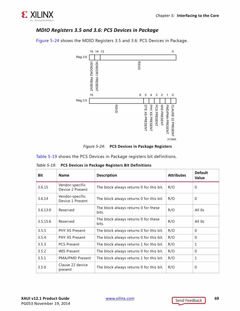
XAUI v12.1 Product Guide www.xilinx.com 69PG053 November 19, 2014
Chapter 5: Interfacing to the Core
MDIO Registers 3.5 and 3.6: PCS Devices in Package
Figure 5-24 shows the MDIO Registers 3.5 and 3.6: PCS Devices in Package.
Table 5-19 shows the PCS Devices in Package registers bit definitions.
X-Ref Target - Figure 5-24
Figure 5-24: PCS Devices in Package Registers
Table 5-19: PCS Devices in Package Registers Bit Definitions
Bit Name Description Attributes Default Value
3.6.15 Vendor-specific Device 2 Present The block always returns 0 for this bit. R/O 0
3.6.14 Vendor-specific Device 1 Present The block always returns 0 for this bit. R/O 0
3.6.13:0 Reserved The block always returns 0 for these bits. R/O All 0s
3.5.15:6 Reserved The block always returns 0 for these bits. R/O All 0s
3.5.5 PHY XS Present The block always returns 0 for this bit. R/O 0
3.5.4 PHY XS Present The block always returns 0 for this bit. R/O 0
3.5.3 PCS Present The block always returns 1 for this bit. R/O 1
3.5.2 WIS Present The block always returns 0 for this bit. R/O 0
3.5.1 PMA/PMD Present The block always returns 1 for this bit. R/O 1
3.5.0 Clause 22 device present The block always returns 0 for this bit. R/O 0
Send Feedback
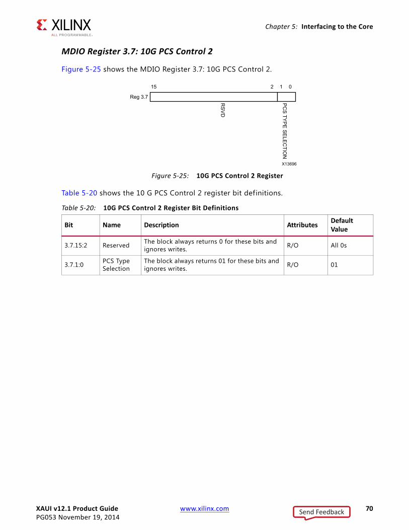
XAUI v12.1 Product Guide www.xilinx.com 70PG053 November 19, 2014
Chapter 5: Interfacing to the Core
MDIO Register 3.7: 10G PCS Control 2
Figure 5-25 shows the MDIO Register 3.7: 10G PCS Control 2.
Table 5-20 shows the 10 G PCS Control 2 register bit definitions.
X-Ref Target - Figure 5-25
Figure 5-25: 10G PCS Control 2 Register
Table 5-20: 10G PCS Control 2 Register Bit Definitions
Bit Name Description Attributes Default Value
3.7.15:2 Reserved The block always returns 0 for these bits and ignores writes. R/O All 0s
3.7.1:0 PCS Type Selection
The block always returns 01 for these bits and ignores writes. R/O 01
Send Feedback
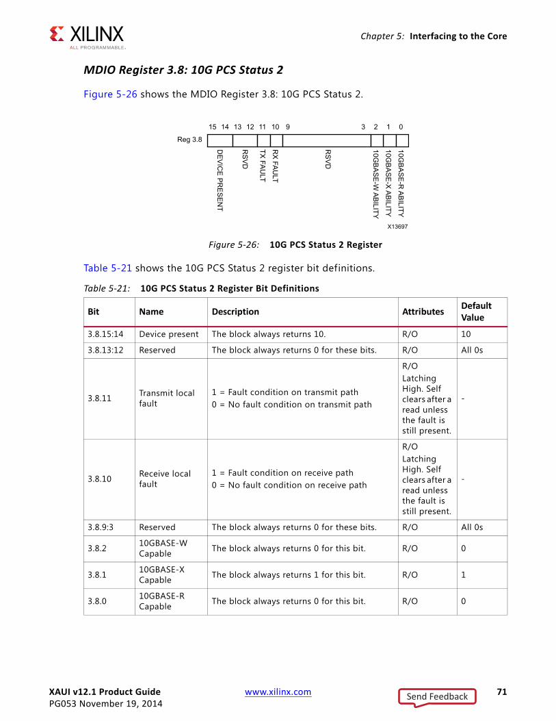
XAUI v12.1 Product Guide www.xilinx.com 71PG053 November 19, 2014
Chapter 5: Interfacing to the Core
MDIO Register 3.8: 10G PCS Status 2
Figure 5-26 shows the MDIO Register 3.8: 10G PCS Status 2.
Table 5-21 shows the 10G PCS Status 2 register bit definitions.
X-Ref Target - Figure 5-26
Figure 5-26: 10G PCS Status 2 Register
Table 5-21: 10G PCS Status 2 Register Bit Definitions
Bit Name Description Attributes Default Value
3.8.15:14 Device present The block always returns 10. R/O 10
3.8.13:12 Reserved The block always returns 0 for these bits. R/O All 0s
3.8.11 Transmit local fault
1 = Fault condition on transmit path0 = No fault condition on transmit path
R/OLatching High. Self clears after a read unless the fault is still present.
-
3.8.10 Receive local fault
1 = Fault condition on receive path0 = No fault condition on receive path
R/OLatching High. Self clears after a read unless the fault is still present.
-
3.8.9:3 Reserved The block always returns 0 for these bits. R/O All 0s
3.8.2 10GBASE-W Capable The block always returns 0 for this bit. R/O 0
3.8.1 10GBASE-X Capable The block always returns 1 for this bit. R/O 1
3.8.0 10GBASE-R Capable The block always returns 0 for this bit. R/O 0
Send Feedback
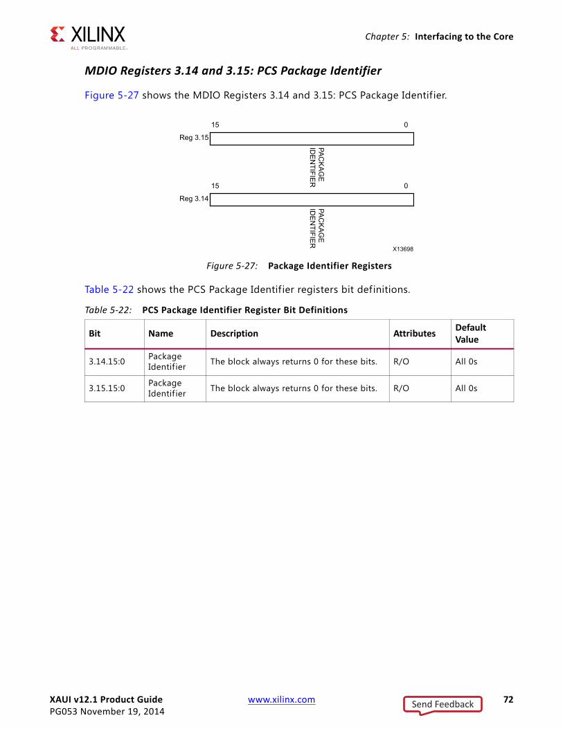
XAUI v12.1 Product Guide www.xilinx.com 72PG053 November 19, 2014
Chapter 5: Interfacing to the Core
MDIO Registers 3.14 and 3.15: PCS Package Identifier
Figure 5-27 shows the MDIO Registers 3.14 and 3.15: PCS Package Identif ier.
Table 5-22 shows the PCS Package Identif ier registers bit definitions.
X-Ref Target - Figure 5-27
Figure 5-27: Package Identifier Registers
Table 5-22: PCS Package Identifier Register Bit Definitions
Bit Name Description Attributes Default Value
3.14.15:0 Package Identif ier The block always returns 0 for these bits. R/O All 0s
3.15.15:0 Package Identif ier The block always returns 0 for these bits. R/O All 0s
Send Feedback
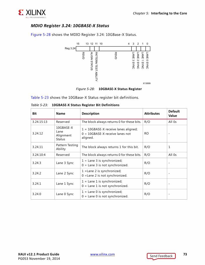
XAUI v12.1 Product Guide www.xilinx.com 73PG053 November 19, 2014
Chapter 5: Interfacing to the Core
MDIO Register 3.24: 10GBASE-X Status
Figure 5-28 shows the MDIO Register 3.24: 10GBase-X Status.
Table 5-23 shows the 10GBase-X Status register bit definitions.
X-Ref Target - Figure 5-28
Figure 5-28: 10GBASE-X Status Register
Table 5-23: 10GBASE-X Status Register Bit Definitions
Bit Name Description Attributes Default Value
3.24.15:13 Reserved The block always returns 0 for these bits. R/O All 0s
3.24.12
10GBASE-X Lane Alignment Status
1 = 10GBASE-X receive lanes aligned;0 = 10GBASE-X receive lanes not aligned.
RO -
3.24.11 Pattern Testing Ability The block always returns 1 for this bit. R/O 1
3.24.10:4 Reserved The block always returns 0 for these bits. R/O All 0s
3.24.3 Lane 3 Sync1 = Lane 3 is synchronized;0 = Lane 3 is not synchronized.
R/O -
3.24.2 Lane 2 Sync1 =Lane 2 is synchronized;0 =Lane 2 is not synchronized.
R/O -
3.24.1 Lane 1 Sync1 = Lane 1 is synchronized;0 = Lane 1 is not synchronized.
R/O -
3.24.0 Lane 0 Sync1 = Lane 0 is synchronized;0 = Lane 0 is not synchronized.
R/O -
Send Feedback
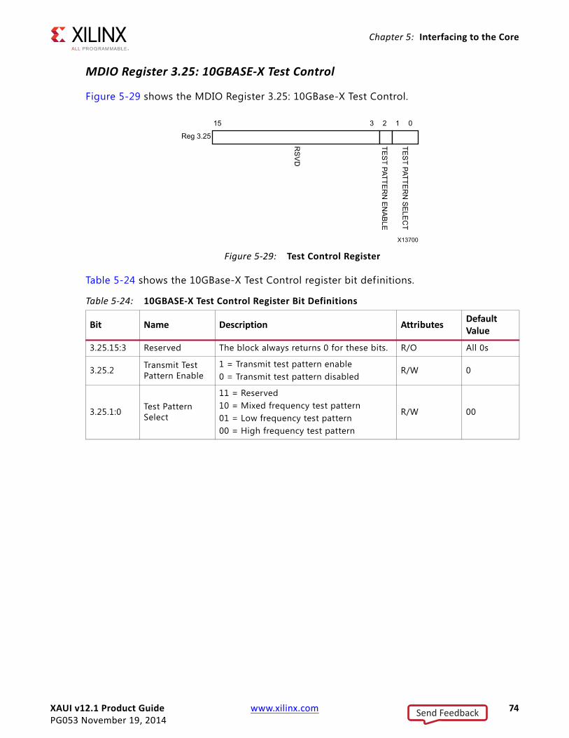
XAUI v12.1 Product Guide www.xilinx.com 74PG053 November 19, 2014
Chapter 5: Interfacing to the Core
MDIO Register 3.25: 10GBASE-X Test Control
Figure 5-29 shows the MDIO Register 3.25: 10GBase-X Test Control.
Table 5-24 shows the 10GBase-X Test Control register bit definitions.
X-Ref Target - Figure 5-29
Figure 5-29: Test Control Register
Table 5-24: 10GBASE-X Test Control Register Bit Definitions
Bit Name Description Attributes Default Value
3.25.15:3 Reserved The block always returns 0 for these bits. R/O All 0s
3.25.2 Transmit Test Pattern Enable
1 = Transmit test pattern enable0 = Transmit test pattern disabled
R/W 0
3.25.1:0 Test Pattern Select
11 = Reserved10 = Mixed frequency test pattern01 = Low frequency test pattern00 = High frequency test pattern
R/W 00
Send Feedback
XAUI v12.1 Product Guide www.xilinx.com 75PG053 November 19, 2014
Chapter 5: Interfacing to the Core
DTE XS MDIO Register MapWhen the core is configured as a DTE XGXS, it occupies MDIO Device Address 5 in the MDIO register address map (Table 5-25).
Table 5-25: DTE XS MDIO Registers
Register Address Register Name
5.0 DTE XS Control 1
5.1 DTE XS Status 1
5.2, 5.3 DTE XS Device Identif ier
5.4 DTE XS Speed Ability
5.5, 5.6 DTE XS Devices in Package
5.7 Reserved
5.8 DTE XS Status 2
5.9 to 5.13 Reserved
5.14, 5.15 DTE XS Package Identif ier
5.16 to 5.23 Reserved
5.24 10G DTE XGXS Lane Status
5.25 10G DTE XGXS Test Control
Send Feedback
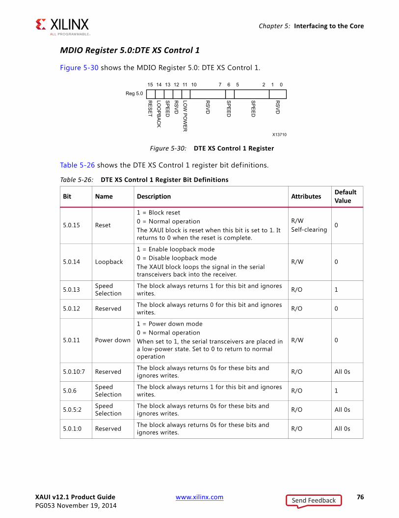
XAUI v12.1 Product Guide www.xilinx.com 76PG053 November 19, 2014
Chapter 5: Interfacing to the Core
MDIO Register 5.0:DTE XS Control 1
Figure 5-30 shows the MDIO Register 5.0: DTE XS Control 1.
Table 5-26 shows the DTE XS Control 1 register bit definitions.
X-Ref Target - Figure 5-30
Figure 5-30: DTE XS Control 1 Register
Table 5-26: DTE XS Control 1 Register Bit Definitions
Bit Name Description Attributes Default Value
5.0.15 Reset
1 = Block reset0 = Normal operationThe XAUI block is reset when this bit is set to 1. It returns to 0 when the reset is complete.
R/WSelf-clearing
0
5.0.14 Loopback
1 = Enable loopback mode0 = Disable loopback modeThe XAUI block loops the signal in the serial transceivers back into the receiver.
R/W 0
5.0.13 Speed Selection
The block always returns 1 for this bit and ignores writes. R/O 1
5.0.12 Reserved The block always returns 0 for this bit and ignores writes. R/O 0
5.0.11 Power down
1 = Power down mode0 = Normal operationWhen set to 1, the serial transceivers are placed in a low-power state. Set to 0 to return to normal operation
R/W 0
5.0.10:7 Reserved The block always returns 0s for these bits and ignores writes. R/O All 0s
5.0.6 Speed Selection
The block always returns 1 for this bit and ignores writes. R/O 1
5.0.5:2 Speed Selection
The block always returns 0s for these bits and ignores writes. R/O All 0s
5.0.1:0 Reserved The block always returns 0s for these bits and ignores writes. R/O All 0s
Send Feedback
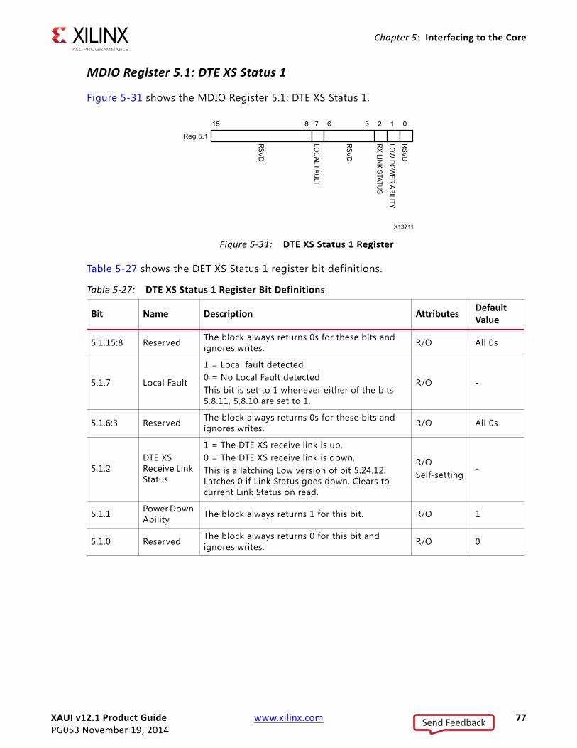
XAUI v12.1 Product Guide www.xilinx.com 77PG053 November 19, 2014
Chapter 5: Interfacing to the Core
MDIO Register 5.1: DTE XS Status 1
Figure 5-31 shows the MDIO Register 5.1: DTE XS Status 1.
Table 5-27 shows the DET XS Status 1 register bit definitions.
X-Ref Target - Figure 5-31
Figure 5-31: DTE XS Status 1 Register
Table 5-27: DTE XS Status 1 Register Bit Definitions
Bit Name Description Attributes Default Value
5.1.15:8 Reserved The block always returns 0s for these bits and ignores writes. R/O All 0s
5.1.7 Local Fault
1 = Local fault detected0 = No Local Fault detectedThis bit is set to 1 whenever either of the bits 5.8.11, 5.8.10 are set to 1.
R/O -
5.1.6:3 Reserved The block always returns 0s for these bits and ignores writes. R/O All 0s
5.1.2DTE XS Receive Link Status
1 = The DTE XS receive link is up.0 = The DTE XS receive link is down.This is a latching Low version of bit 5.24.12. Latches 0 if Link Status goes down. Clears to current Link Status on read.
R/OSelf-setting
-
5.1.1 Power Down Ability The block always returns 1 for this bit. R/O 1
5.1.0 Reserved The block always returns 0 for this bit and ignores writes. R/O 0
Send Feedback
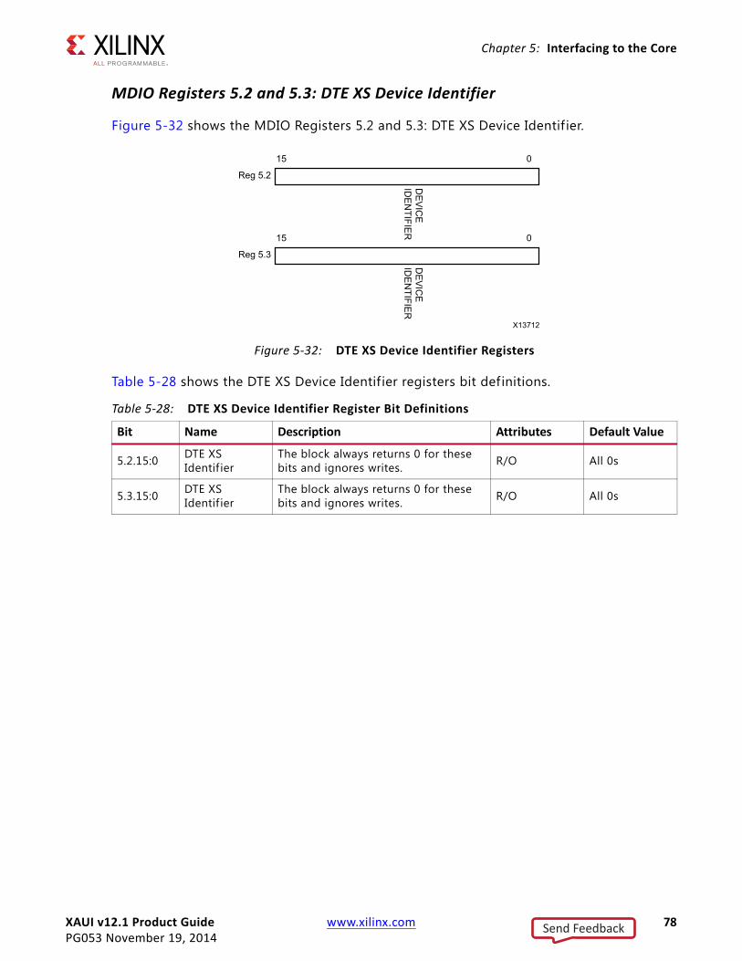
XAUI v12.1 Product Guide www.xilinx.com 78PG053 November 19, 2014
Chapter 5: Interfacing to the Core
MDIO Registers 5.2 and 5.3: DTE XS Device Identifier
Figure 5-32 shows the MDIO Registers 5.2 and 5.3: DTE XS Device Identif ier.
Table 5-28 shows the DTE XS Device Identif ier registers bit definitions.
X-Ref Target - Figure 5-32
Figure 5-32: DTE XS Device Identifier Registers
Table 5-28: DTE XS Device Identifier Register Bit Definitions
Bit Name Description Attributes Default Value
5.2.15:0 DTE XS Identif ier
The block always returns 0 for these bits and ignores writes. R/O All 0s
5.3.15:0 DTE XS Identif ier
The block always returns 0 for these bits and ignores writes. R/O All 0s
Send Feedback
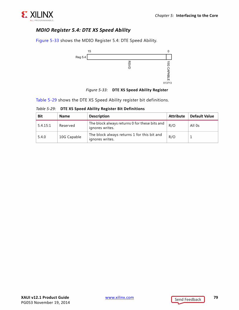
XAUI v12.1 Product Guide www.xilinx.com 79PG053 November 19, 2014
Chapter 5: Interfacing to the Core
MDIO Register 5.4: DTE XS Speed Ability
Figure 5-33 shows the MDIO Register 5.4: DTE Speed Ability.
Table 5-29 shows the DTE XS Speed Ability register bit definitions.
X-Ref Target - Figure 5-33
Figure 5-33: DTE XS Speed Ability Register
Table 5-29: DTE XS Speed Ability Register Bit Definitions
Bit Name Description Attribute Default Value
5.4.15:1 Reserved The block always returns 0 for these bits and ignores writes. R/O All 0s
5.4.0 10G Capable The block always returns 1 for this bit and ignores writes. R/O 1
Send Feedback
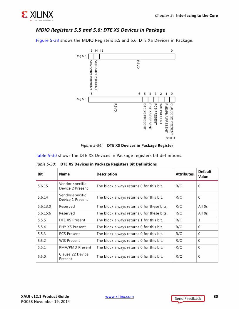
XAUI v12.1 Product Guide www.xilinx.com 80PG053 November 19, 2014
Chapter 5: Interfacing to the Core
MDIO Registers 5.5 and 5.6: DTE XS Devices in Package
Figure 5-33 shows the MDIO Registers 5.5 and 5.6: DTE XS Devices in Package.
Table 5-30 shows the DTE XS Devices in Package registers bit definitions.
X-Ref Target - Figure 5-34
Figure 5-34: DTE XS Devices in Package Register
Table 5-30: DTE XS Devices in Package Registers Bit Definitions
Bit Name Description Attributes Default Value
5.6.15 Vendor-specif ic Device 2 Present The block always returns 0 for this bit. R/O 0
5.6.14 Vendor-specif ic Device 1 Present The block always returns 0 for this bit. R/O 0
5.6.13:0 Reserved The block always returns 0 for these bits. R/O All 0s
5.6.15:6 Reserved The block always returns 0 for these bits. R/O All 0s
5.5.5 DTE XS Present The block always returns 1 for this bit. R/O 1
5.5.4 PHY XS Present The block always returns 0 for this bit. R/O 0
5.5.3 PCS Present The block always returns 0 for this bit. R/O 0
5.5.2 WIS Present The block always returns 0 for this bit. R/O 0
5.5.1 PMA/PMD Present The block always returns 0 for this bit. R/O 0
5.5.0 Clause 22 Device Present The block always returns 0 for this bit. R/O 0
Send Feedback
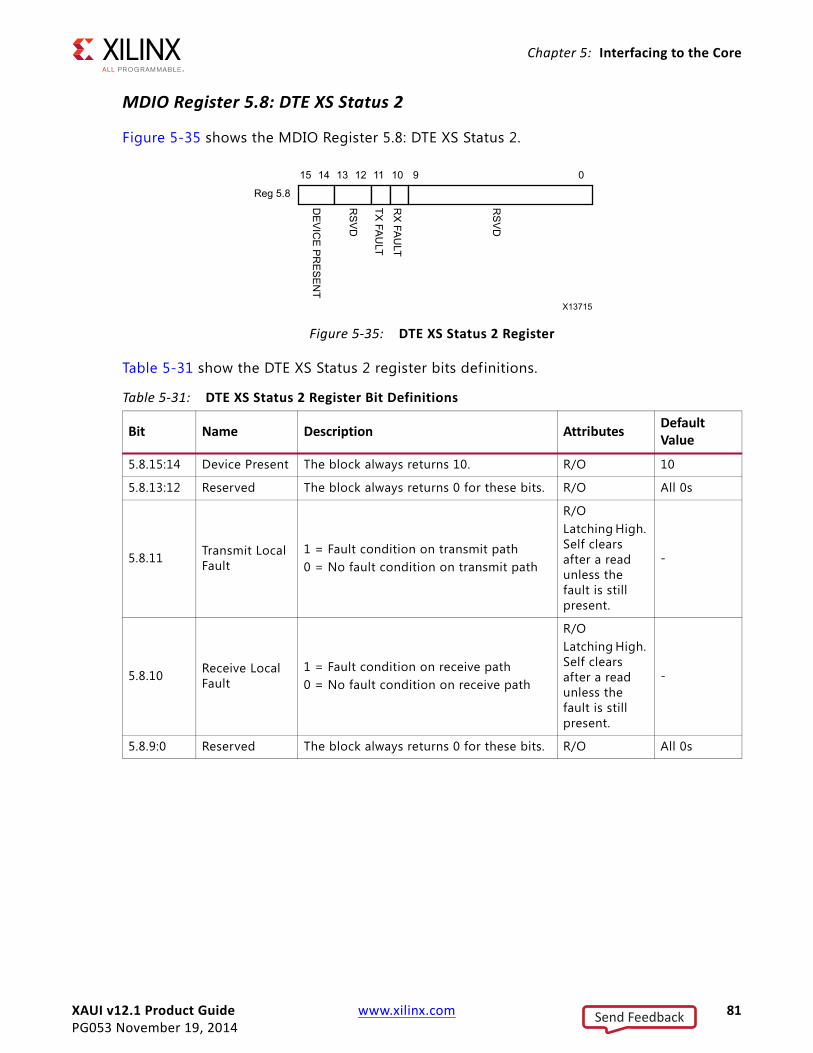
XAUI v12.1 Product Guide www.xilinx.com 81PG053 November 19, 2014
Chapter 5: Interfacing to the Core
MDIO Register 5.8: DTE XS Status 2
Figure 5-35 shows the MDIO Register 5.8: DTE XS Status 2.
Table 5-31 show the DTE XS Status 2 register bits definitions.
X-Ref Target - Figure 5-35
Figure 5-35: DTE XS Status 2 Register
Table 5-31: DTE XS Status 2 Register Bit Definitions
Bit Name Description Attributes Default Value
5.8.15:14 Device Present The block always returns 10. R/O 10
5.8.13:12 Reserved The block always returns 0 for these bits. R/O All 0s
5.8.11 Transmit Local Fault
1 = Fault condition on transmit path0 = No fault condition on transmit path
R/OLatching High. Self clears after a read unless the fault is still present.
-
5.8.10 Receive Local Fault
1 = Fault condition on receive path0 = No fault condition on receive path
R/OLatching High. Self clears after a read unless the fault is still present.
-
5.8.9:0 Reserved The block always returns 0 for these bits. R/O All 0s
Send Feedback
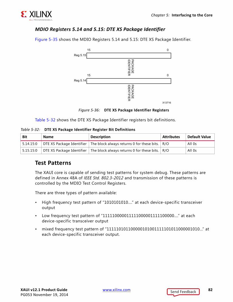
XAUI v12.1 Product Guide www.xilinx.com 82PG053 November 19, 2014
Chapter 5: Interfacing to the Core
MDIO Registers 5.14 and 5.15: DTE XS Package Identifier
Figure 5-35 shows the MDIO Registers 5.14 and 5.15: DTE XS Package Identif ier.
Table 5-32 shows the DTE XS Package Identif ier registers bit definitions.
Test PatternsThe XAUI core is capable of sending test patterns for system debug. These patterns are defined in Annex 48A of IEEE Std. 802.3-2012 and transmission of these patterns is controlled by the MDIO Test Control Registers.
There are three types of pattern available:
• High frequency test pattern of “1010101010....” at each device-specif ic transceiver output
• Low frequency test pattern of “111110000011111000001111100000....” at each device-specific transceiver output
• mixed frequency test pattern of “111110101100000101001111101011000001010...” at each device-specif ic transceiver output.
X-Ref Target - Figure 5-36
Figure 5-36: DTE XS Package Identifier Registers
Table 5-32: DTE XS Package Identifier Register Bit Definitions
Bit Name Description Attributes Default Value
5.14.15:0 DTE XS Package Identif ier The block always returns 0 for these bits. R/O All 0s
5.15.15:0 DTE XS Package Identif ier The block always returns 0 for these bits. R/O All 0s
Send Feedback

XAUI v12.1 Product Guide www.xilinx.com 83PG053 November 19, 2014
Chapter 5: Interfacing to the Core
MDIO Register 5.24: DTE XS Lane Status
Figure 5-37 shows the MDIO Register 5.24: DTE XS Lane Status.
Table 5-33 shows the DTE XS Lane Status register bit definitions.
X-Ref Target - Figure 5-37
Figure 5-37: DTE XS Lane Status Register
Table 5-33: DTE XS Lane Status Register Bit Definitions
Bit Name Description Attributes Default Value
5.24.15:13 Reserved The block always returns 0 for these bits. R/O All 0s
5.24.12DTE XGXS Lane Alignment Status
1 = DTE XGXS receive lanes aligned0 = DTE XGXS receive lanes not aligned
R/O -
5.24.11 Pattern testing ability The block always returns 1 for this bit. R/O 1
5.24.10:4 Reserved The block always returns 0 for these bits. R/O All 0s
5.24.3 Lane 3 Sync1 = Lane 3 is synchronized;0 = Lane 3 is not synchronized.
R/O -
5.24.2 Lane 2 Sync1 = Lane 2 is synchronized;0 = Lane 2 is not synchronized.
R/O -
5.24.1 Lane 1 Sync1 = Lane 1 is synchronized;0 = Lane 1 is not synchronized.
R/O -
5.24.0 Lane 0 Sync1 = Lane 0 is synchronized;0 = Lane 0 is not synchronized.
R/O -
Send Feedback
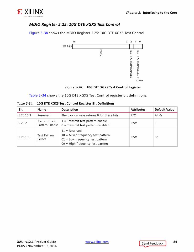
XAUI v12.1 Product Guide www.xilinx.com 84PG053 November 19, 2014
Chapter 5: Interfacing to the Core
MDIO Register 5.25: 10G DTE XGXS Test Control
Figure 5-38 shows the MDIO Register 5.25: 10G DTE XGXS Test Control.
Table 5-34 shows the 10G DTE XGXS Test Control register bit definitions.
X-Ref Target - Figure 5-38
Figure 5-38: 10G DTE XGXS Test Control Register
Table 5-34: 10G DTE XGXS Test Control Register Bit Definitions
Bit Name Description Attributes Default Value
5.25.15:3 Reserved The block always returns 0 for these bits. R/O All 0s
5.25.2 Transmit Test Pattern Enable
1 = Transmit test pattern enable0 = Transmit test pattern disabled
R/W 0
5.25.1:0 Test Pattern Select
11 = Reserved10 = Mixed frequency test pattern01 = Low frequency test pattern00 = High frequency test pattern
R/W 00
Send Feedback
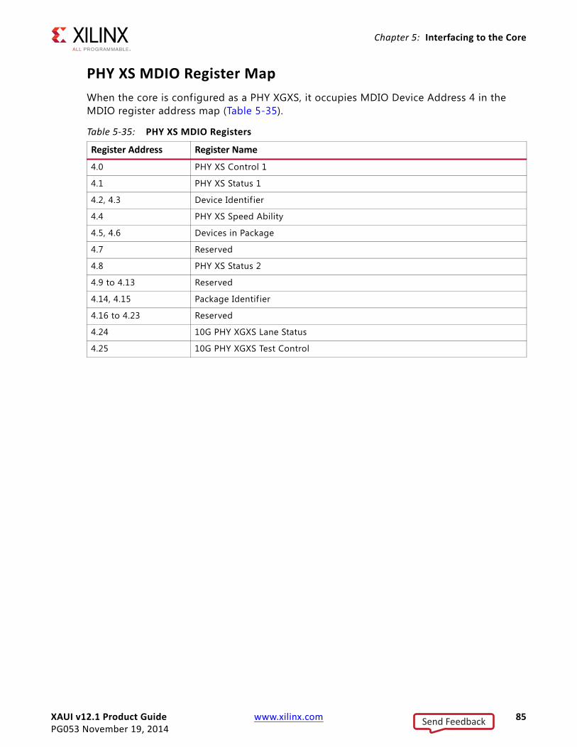
XAUI v12.1 Product Guide www.xilinx.com 85PG053 November 19, 2014
Chapter 5: Interfacing to the Core
PHY XS MDIO Register MapWhen the core is configured as a PHY XGXS, it occupies MDIO Device Address 4 in the MDIO register address map (Table 5-35).
Table 5-35: PHY XS MDIO Registers
Register Address Register Name
4.0 PHY XS Control 1
4.1 PHY XS Status 1
4.2, 4.3 Device Identif ier
4.4 PHY XS Speed Ability
4.5, 4.6 Devices in Package
4.7 Reserved
4.8 PHY XS Status 2
4.9 to 4.13 Reserved
4.14, 4.15 Package Identif ier
4.16 to 4.23 Reserved
4.24 10G PHY XGXS Lane Status
4.25 10G PHY XGXS Test Control
Send Feedback
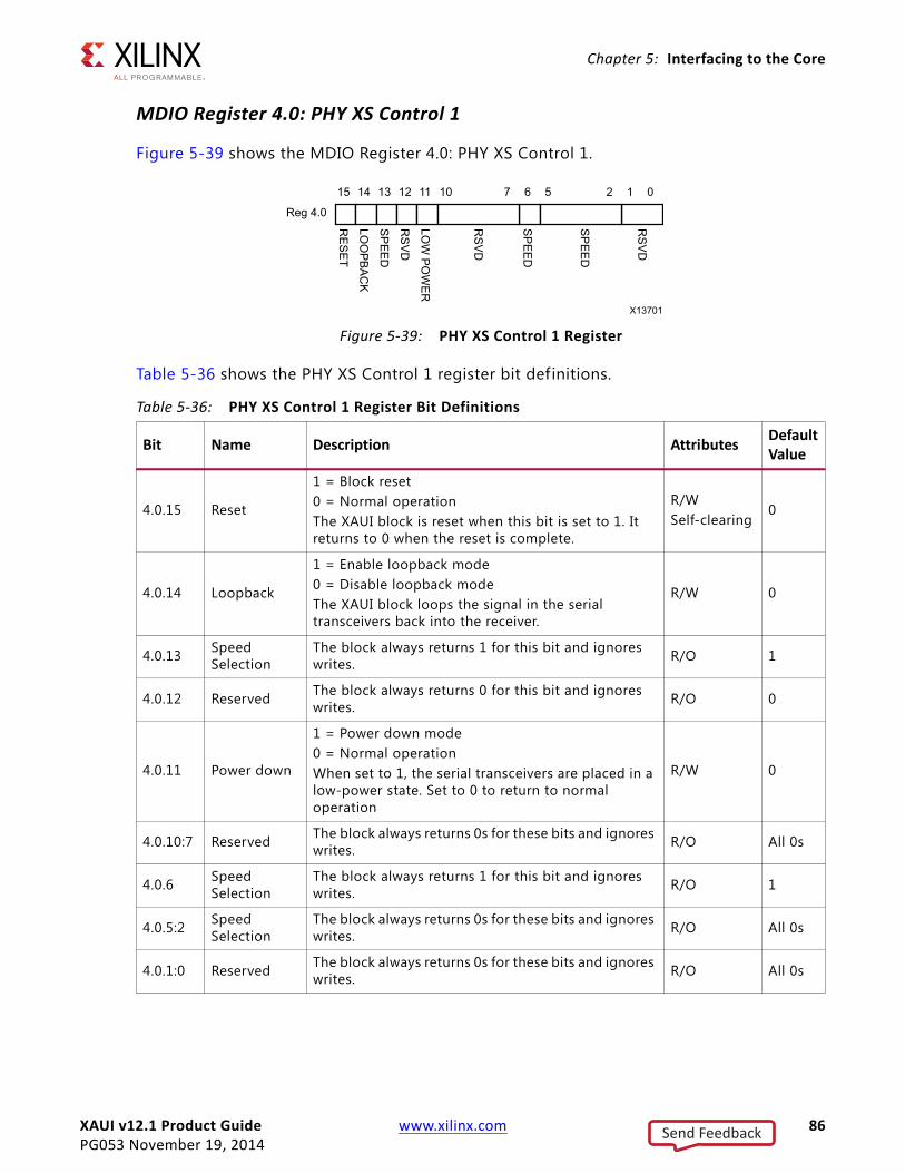
XAUI v12.1 Product Guide www.xilinx.com 86PG053 November 19, 2014
Chapter 5: Interfacing to the Core
MDIO Register 4.0: PHY XS Control 1
Figure 5-39 shows the MDIO Register 4.0: PHY XS Control 1.
Table 5-36 shows the PHY XS Control 1 register bit definitions.
X-Ref Target - Figure 5-39
Figure 5-39: PHY XS Control 1 Register
Table 5-36: PHY XS Control 1 Register Bit Definitions
Bit Name Description Attributes Default Value
4.0.15 Reset
1 = Block reset0 = Normal operationThe XAUI block is reset when this bit is set to 1. It returns to 0 when the reset is complete.
R/WSelf-clearing
0
4.0.14 Loopback
1 = Enable loopback mode0 = Disable loopback modeThe XAUI block loops the signal in the serial transceivers back into the receiver.
R/W 0
4.0.13 Speed Selection
The block always returns 1 for this bit and ignores writes. R/O 1
4.0.12 Reserved The block always returns 0 for this bit and ignores writes. R/O 0
4.0.11 Power down
1 = Power down mode0 = Normal operationWhen set to 1, the serial transceivers are placed in a low-power state. Set to 0 to return to normal operation
R/W 0
4.0.10:7 Reserved The block always returns 0s for these bits and ignores writes. R/O All 0s
4.0.6 Speed Selection
The block always returns 1 for this bit and ignores writes. R/O 1
4.0.5:2 Speed Selection
The block always returns 0s for these bits and ignores writes. R/O All 0s
4.0.1:0 Reserved The block always returns 0s for these bits and ignores writes. R/O All 0s
Send Feedback

XAUI v12.1 Product Guide www.xilinx.com 87PG053 November 19, 2014
Chapter 5: Interfacing to the Core
MDIO Register 4.1: PHY XS Status 1
Figure 5-40 shows the MDIO Register 4.1: PHY XS Status 1.
Table 5-37 shows the PHY XS Status 1 register bit definitions.
X-Ref Target - Figure 5-40
Figure 5-40: PHY XS Status 1 Register
Table 5-37: PHY XS Status 1 Register Bit Definitions
Bit Name Description Attributes Default Value
4.1.15:8 Reserved The block always returns 0s for these bits and ignores writes. R/O All 0s
4.1.7 Local Fault
1 = Local fault detected0 = No Local Fault detectedThis bit is set to 1 whenever either of the bits 4.8.11, 4.8.10 are set to 1.
R/O -
4.1.6:3 Reserved The block always returns 0s for these bits and ignores writes. R/O All 0s
4.1.2 PHY XS Receive Link Status
1 = The PHY XS receive link is up.0 =The PHY XS receive link is down.This is a latching Low version of bit 4.24.12. Latches 0 if Link Status goes down. Clears to current Link Status on read.
R/OSelf-setting
-
4.1.1 Power Down Ability The block always returns 1 for this bit. R/O 1
4.1.0 Reserved The block always returns 0 for this bit and ignores writes. R/O 0
Send Feedback
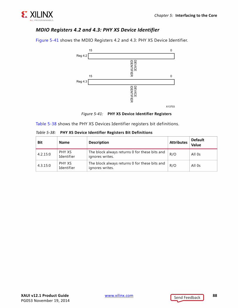
XAUI v12.1 Product Guide www.xilinx.com 88PG053 November 19, 2014
Chapter 5: Interfacing to the Core
MDIO Registers 4.2 and 4.3: PHY XS Device Identifier
Figure 5-41 shows the MDIO Registers 4.2 and 4.3: PHY XS Device Identif ier.
Table 5-38 shows the PHY XS Devices Identif ier registers bit definitions.
X-Ref Target - Figure 5-41
Figure 5-41: PHY XS Device Identifier Registers
Table 5-38: PHY XS Device Identifier Registers Bit Definitions
Bit Name Description Attributes Default Value
4.2.15:0 PHY XS Identif ier
The block always returns 0 for these bits and ignores writes. R/O All 0s
4.3.15:0 PHY XS Identif ier
The block always returns 0 for these bits and ignores writes. R/O All 0s
Send Feedback
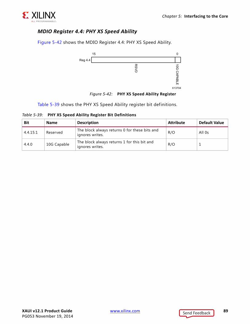
XAUI v12.1 Product Guide www.xilinx.com 89PG053 November 19, 2014
Chapter 5: Interfacing to the Core
MDIO Register 4.4: PHY XS Speed Ability
Figure 5-42 shows the MDIO Register 4.4: PHY XS Speed Ability.
Table 5-39 shows the PHY XS Speed Ability register bit definitions.
X-Ref Target - Figure 5-42
Figure 5-42: PHY XS Speed Ability Register
Table 5-39: PHY XS Speed Ability Register Bit Definitions
Bit Name Description Attribute Default Value
4.4.15:1 Reserved The block always returns 0 for these bits and ignores writes. R/O All 0s
4.4.0 10G Capable The block always returns 1 for this bit and ignores writes. R/O 1
Send Feedback
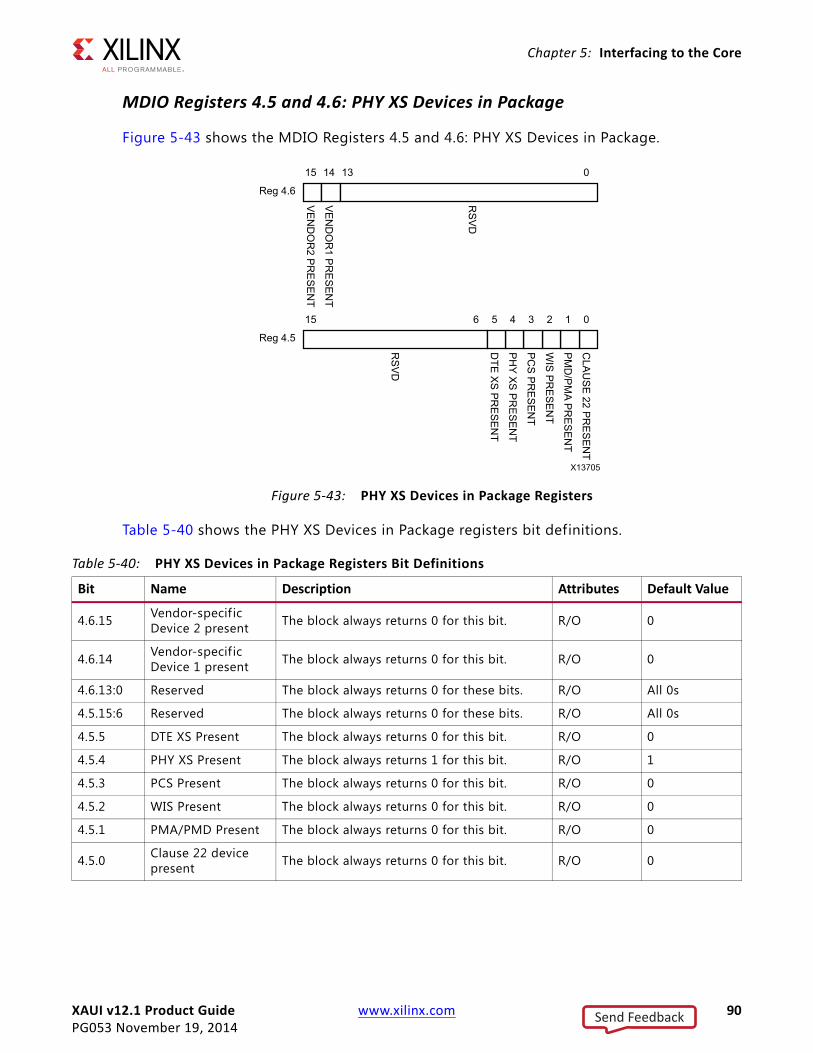
XAUI v12.1 Product Guide www.xilinx.com 90PG053 November 19, 2014
Chapter 5: Interfacing to the Core
MDIO Registers 4.5 and 4.6: PHY XS Devices in Package
Figure 5-43 shows the MDIO Registers 4.5 and 4.6: PHY XS Devices in Package.
Table 5-40 shows the PHY XS Devices in Package registers bit definitions.
X-Ref Target - Figure 5-43
Figure 5-43: PHY XS Devices in Package Registers
Table 5-40: PHY XS Devices in Package Registers Bit Definitions
Bit Name Description Attributes Default Value
4.6.15 Vendor-specif ic Device 2 present The block always returns 0 for this bit. R/O 0
4.6.14 Vendor-specif ic Device 1 present The block always returns 0 for this bit. R/O 0
4.6.13:0 Reserved The block always returns 0 for these bits. R/O All 0s
4.5.15:6 Reserved The block always returns 0 for these bits. R/O All 0s
4.5.5 DTE XS Present The block always returns 0 for this bit. R/O 0
4.5.4 PHY XS Present The block always returns 1 for this bit. R/O 1
4.5.3 PCS Present The block always returns 0 for this bit. R/O 0
4.5.2 WIS Present The block always returns 0 for this bit. R/O 0
4.5.1 PMA/PMD Present The block always returns 0 for this bit. R/O 0
4.5.0 Clause 22 device present The block always returns 0 for this bit. R/O 0
Send Feedback
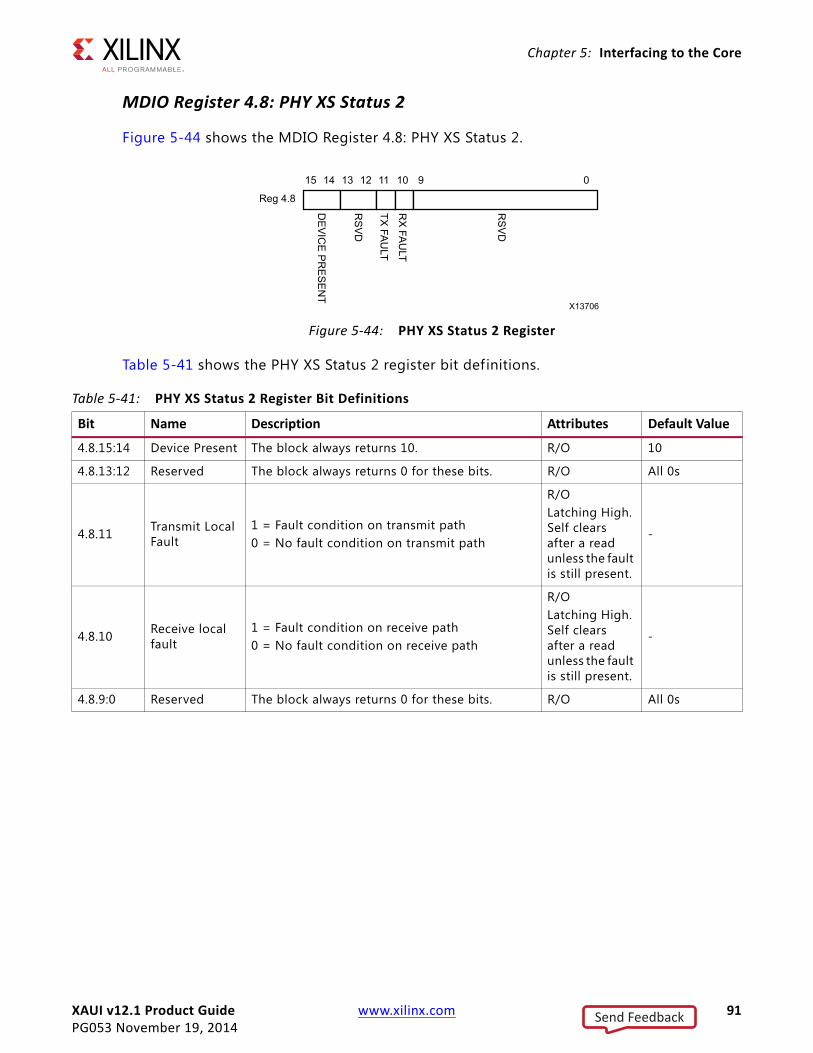
XAUI v12.1 Product Guide www.xilinx.com 91PG053 November 19, 2014
Chapter 5: Interfacing to the Core
MDIO Register 4.8: PHY XS Status 2
Figure 5-44 shows the MDIO Register 4.8: PHY XS Status 2.
Table 5-41 shows the PHY XS Status 2 register bit definitions.
X-Ref Target - Figure 5-44
Figure 5-44: PHY XS Status 2 Register
Table 5-41: PHY XS Status 2 Register Bit Definitions
Bit Name Description Attributes Default Value
4.8.15:14 Device Present The block always returns 10. R/O 10
4.8.13:12 Reserved The block always returns 0 for these bits. R/O All 0s
4.8.11 Transmit Local Fault
1 = Fault condition on transmit path0 = No fault condition on transmit path
R/OLatching High. Self clears after a read unless the fault is still present.
-
4.8.10 Receive local fault
1 = Fault condition on receive path0 = No fault condition on receive path
R/OLatching High. Self clears after a read unless the fault is still present.
-
4.8.9:0 Reserved The block always returns 0 for these bits. R/O All 0s
Send Feedback
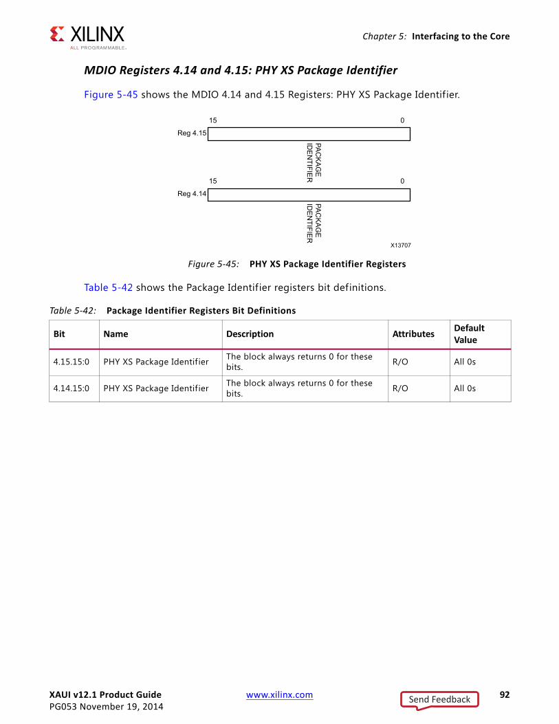
XAUI v12.1 Product Guide www.xilinx.com 92PG053 November 19, 2014
Chapter 5: Interfacing to the Core
MDIO Registers 4.14 and 4.15: PHY XS Package Identifier
Figure 5-45 shows the MDIO 4.14 and 4.15 Registers: PHY XS Package Identif ier.
Table 5-42 shows the Package Identif ier registers bit definitions.
X-Ref Target - Figure 5-45
Figure 5-45: PHY XS Package Identifier Registers
Table 5-42: Package Identifier Registers Bit Definitions
Bit Name Description Attributes Default Value
4.15.15:0 PHY XS Package Identif ier The block always returns 0 for these bits. R/O All 0s
4.14.15:0 PHY XS Package Identif ier The block always returns 0 for these bits. R/O All 0s
Send Feedback
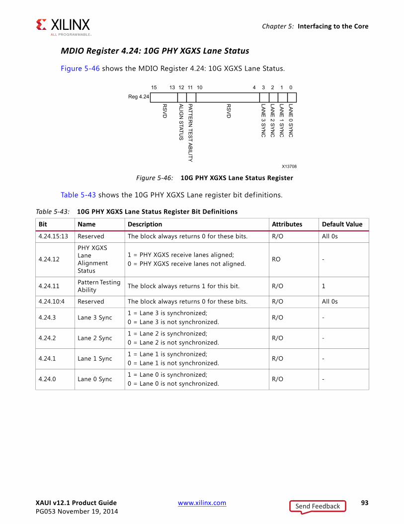
XAUI v12.1 Product Guide www.xilinx.com 93PG053 November 19, 2014
Chapter 5: Interfacing to the Core
MDIO Register 4.24: 10G PHY XGXS Lane Status
Figure 5-46 shows the MDIO Register 4.24: 10G XGXS Lane Status.
Table 5-43 shows the 10G PHY XGXS Lane register bit definitions.
X-Ref Target - Figure 5-46
Figure 5-46: 10G PHY XGXS Lane Status Register
Table 5-43: 10G PHY XGXS Lane Status Register Bit Definitions
Bit Name Description Attributes Default Value
4.24.15:13 Reserved The block always returns 0 for these bits. R/O All 0s
4.24.12
PHY XGXS Lane Alignment Status
1 = PHY XGXS receive lanes aligned;0 = PHY XGXS receive lanes not aligned.
RO -
4.24.11 Pattern Testing Ability The block always returns 1 for this bit. R/O 1
4.24.10:4 Reserved The block always returns 0 for these bits. R/O All 0s
4.24.3 Lane 3 Sync1 = Lane 3 is synchronized;0 = Lane 3 is not synchronized.
R/O -
4.24.2 Lane 2 Sync1 = Lane 2 is synchronized;0 = Lane 2 is not synchronized.
R/O -
4.24.1 Lane 1 Sync1 = Lane 1 is synchronized;0 = Lane 1 is not synchronized.
R/O -
4.24.0 Lane 0 Sync1 = Lane 0 is synchronized;0 = Lane 0 is not synchronized.
R/O -
Send Feedback
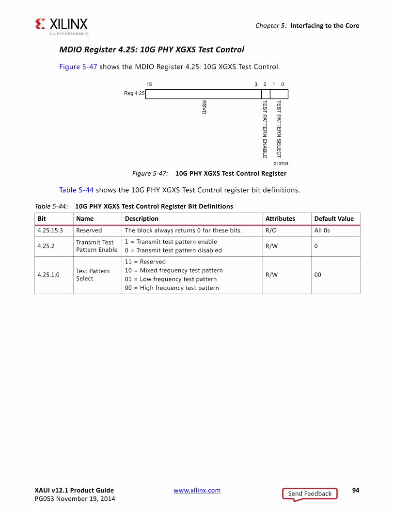
XAUI v12.1 Product Guide www.xilinx.com 94PG053 November 19, 2014
Chapter 5: Interfacing to the Core
MDIO Register 4.25: 10G PHY XGXS Test Control
Figure 5-47 shows the MDIO Register 4.25: 10G XGXS Test Control.
Table 5-44 shows the 10G PHY XGXS Test Control register bit definitions.
X-Ref Target - Figure 5-47
Figure 5-47: 10G PHY XGXS Test Control Register
Table 5-44: 10G PHY XGXS Test Control Register Bit Definitions
Bit Name Description Attributes Default Value
4.25.15:3 Reserved The block always returns 0 for these bits. R/O All 0s
4.25.2 Transmit Test Pattern Enable
1 = Transmit test pattern enable0 = Transmit test pattern disabled
R/W 0
4.25.1:0 Test Pattern Select
11 = Reserved10 = Mixed frequency test pattern01 = Low frequency test pattern00 = High frequency test pattern
R/W 00
Send Feedback
XAUI v12.1 Product Guide www.xilinx.com 95PG053 November 19, 2014
Chapter 5: Interfacing to the Core
Configuration and Status VectorsIf the XAUI core is generated without an MDIO interface, the key configuration and status information is carried on simple bit vectors, which are:
• configuration_vector[6:0]
• status_vector[7:0]
Table 5-45 shows the Configuration Vector bit definitions.
Table 5-45: Configuration Vector Bit Definitions
Bit Name Description
0 Loopback Sets serial loopback in the device-specif ic transceivers. See bit 5.0.14 in Table 5-26.
1 Power Down Sets the device-specific transceivers into power down mode. See bit 5.0.11 in Table 5-26.
2 Reset Local FaultClears both TX Local Fault and RX Local Fault bits (status_vector[0] and status_vector[1]). See Table 5-46. This bit should be driven by a register on the same clock domain as the XAUI core.
3 Reset Rx Link StatusSets the RX Link Status bit (status_vector[7]). See Table 5-46. This bit should be driven by a register on the same clock domain as the XAUI core.
4 Test Enable Enables transmit test pattern generation. See bit 5.25.2 in Table 5-34.
6:5 Test Select(1:0) Selects the test pattern. See bits 5.25.1:0 in Table 5-34.
Send Feedback
XAUI v12.1 Product Guide www.xilinx.com 96PG053 November 19, 2014
Chapter 5: Interfacing to the Core
Table 5-46 shows the Status Vector bit definitions.
Bits 0 and 1 of the status_vector port, the “Local Fault” bits, are latching-high and cleared Low by bit 2 of the configuration_vector port. Figure 5-48 shows how the status bits are cleared.
Bit 7 of the status_vector port, the “RX Link Status” bit, is latching-Low and set High by bit 3 of the configuration vector. Figure 5-49 shows how the status bit is set.
Table 5-46: Status Vector Bit Definitions
Bit Name Description
0 Tx Local Fault1 if there is a fault in the transmit path, otherwise 0; see bit 5.8.11 in Table 5-31. Latches High. Cleared by rising edge on configuration_vector[2].
1 Rx Local Fault1 if there is a fault in the receive path, otherwise 0; see bit 5.8.10 in Table 5-31. Latches High. Cleared by rising edge on configuration_vector[2].
5:2 Synchronization
Each bit is 1 if the corresponding XAUI lane is synchronized on receive, otherwise 0; see bits 5.24.3:0 in Table 5-32. These four bits are also used to generate the sync_status[3:0] signal described in Table 5-47.
6 Alignment
1 if the XAUI receiver is aligned over all four lanes, otherwise 0; see bit 5.24.12 in Table 5-32. This is also used to generate the align_status signal described in Table 5-47.
7 Rx Link Status1 if the Receiver link is up, otherwise 0; see bit 5.1.2 in Table 5-27. Latches Low. Cleared by rising edge on configuration_vector[3].
X-Ref Target - Figure 5-48
Figure 5-48: Clearing the Local Fault Status Bits
X-Ref Target - Figure 5-49
Figure 5-49: Setting the RX Link Status Bit
Send Feedback
XAUI v12.1 Product Guide www.xilinx.com 97PG053 November 19, 2014
Chapter 5: Interfacing to the Core
Debug PortIn addition to the configuration and status interfaces described in the previous section, there are always available two output ports signaling the alignment and synchronization status of the receiver. (Table 5-47.)
Table 5-47: Debug Port
Port Name Description
debug[5] align_status: 1 when the XAUI receiver is aligned across all four lanes, 0 otherwise.
debug[4:1] sync_status: Each pin is 1 when the respective XAUI lane receiver is synchronized to byte boundaries, 0 otherwise.
debug[0] Indicates when the TX phase alignment of the transceiver has been completed.
Send Feedback
XAUI v12.1 Product Guide www.xilinx.com 98PG053 November 19, 2014
Chapter 6
Design ConsiderationsThis chapter describes considerations that might apply in particular design cases.
Shared LogicXAUI provides the possibility to include the logic related to the reference clock inside the actual core. Using the shared logic feature, you can choose whether to include the logic for the generation of the reference clock in the example design, as it was in previous versions, or inside the core, simplifying the design.
This new level of hierarchy receives the name of <component_name>_support. Figure 6-1 and Figure 6-2 show the two different configurations of the example design depending on whether the shared logic is included in the core or not. The Shared Logic option is set in the Vivado® IDE, as shown Figure 7-1.
X-Ref Target - Figure 6-1
Figure 6-1: Shared Logic Included in the Core
Send Feedback
XAUI v12.1 Product Guide www.xilinx.com 99PG053 November 19, 2014
Chapter 6: Design Considerations
Clocking: UltraScale ArchitectureThe clocking schemes in this section are illustrative only and might require customization for a specific application.
Reference Clock
10G—XAUI
The transceivers use a reference clock of 156.25 MHz to operate at a line rate of 3.125 Gb/s.
20G—XAUI
The transceivers use a reference clock of 312.5 MHz to operate at a line rate of 6.25 Gb/s.
UltraScale Device GTH TransceiversA single IBUFDS_GTE3 module is used to feed the reference clock to the GTHE3_COMMON transceiver Quad PLL (QPLL). This module can be included inside the core as part of the shared logic if this is included in the core instead of the example design. See Figure 6-6 and Figure 6-10 respectively for the shared logic to be included in the example design or in the core.
For more information about UltraScale device transceiver clock distribution, see the UltraScale Architecture GTH Transceivers User Guide (UG576) [Ref 3]
X-Ref Target - Figure 6-2
Figure 6-2: Shared Logic Included in Example Design
Send Feedback
XAUI v12.1 Product Guide www.xilinx.com 100PG053 November 19, 2014
Chapter 6: Design Considerations
Clocking: Zynq-7000, Virtex-7, Artix-7, and Kintex-7 Devices The clocking schemes in this section are illustrative only and might require customization for a specific application.
Reference Clock
10G — XAUI
The transceivers use a reference clock of 156.25 MHz to operate at a line rate of 3.125 Gb/s.
20G — XAUI
The transceivers use a reference clock of 312.5 MHz to operate at a line rate of 6.25 Gb/s.
7 Series FPGA GTH Transceivers A single IBUFDS_GTE2 module is used to feed the reference clock to the GTHE2_CHANNEL PLL (CPLL). This module can be included inside the core as part of the shared logic if this is included in the core instead of the example design. See Figure 6-4 and Figure 6-8 respectively for the shared logic to be included in the example design or in the core.
For more information about 7 series FPGA transceiver clock distribution, see the section on Clocking in the 7 Series FPGAs GTX/GTH Transceiver User Guide (UG476) [Ref 1].
7 Series FPGA GTX TransceiversA single IBUFDS_GTE2 module is used to feed the reference clock to GTXE2_COMMON transceiver Quad PLL (QPLL). This module can be included inside the core as part of the shared logic if this is included in the core instead of the example design. See Figure 6-5 and Figure 6-9 respectively for the shared logic to be included in the example design or in the core.
For more information about 7 series FPGA transceiver clock distribution, see the section on Clocking in the 7 Series FPGAs GTX/GTH Transceiver User Guide (UG476) [Ref 1].
7 Series FPGA GTP TransceiversA single IBUFDS_GTE2 module is used to feed the reference clock to the GTPE2_COMMON PLL. This module can be included inside the core as part of the shared logic if this is included in the core instead of the example design. See Figure 6-3 and Figure 6-7 respectively for the shared logic to be included in the example design or in the core.
Send Feedback
XAUI v12.1 Product Guide www.xilinx.com 101PG053 November 19, 2014
Chapter 6: Design Considerations
For more information about 7 series FPGA transceiver clock distribution, see the section on clocking in the 7 Series FPGAs GTP Transceiver User Guide (UG482) [Ref 2].
Internal Client-Side Interface for 10G – XAUIThe clocking schemes when shared logic is in the example design is shown in Figure 6-3 (GTP transceivers), Figure 6-4 (GTH transceivers), and Figure 6-5 (GTX transceivers) for 7 series FPGAs, and Figure 6-6 (GTH transceivers) for UltraScale devices.
X-Ref Target - Figure 6-3
Figure 6-3: Clock Scheme for Internal Client-Side Interface 7 Series FPGA GTP Transceiver Shared Logic in Example Design
Send Feedback
XAUI v12.1 Product Guide www.xilinx.com 102PG053 November 19, 2014
Chapter 6: Design Considerations
X-Ref Target - Figure 6-4
Figure 6-4: Clock Scheme for Internal Client-Side Interface 7 Series FPGA GTH Transceiver Shared Logic in Example Design
Send Feedback
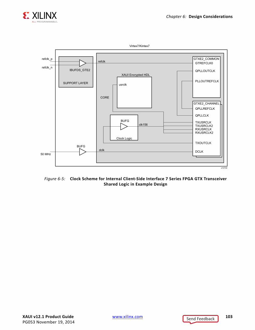
XAUI v12.1 Product Guide www.xilinx.com 103PG053 November 19, 2014
Chapter 6: Design Considerations
X-Ref Target - Figure 6-5
Figure 6-5: Clock Scheme for Internal Client-Side Interface 7 Series FPGA GTX Transceiver Shared Logic in Example Design
Send Feedback
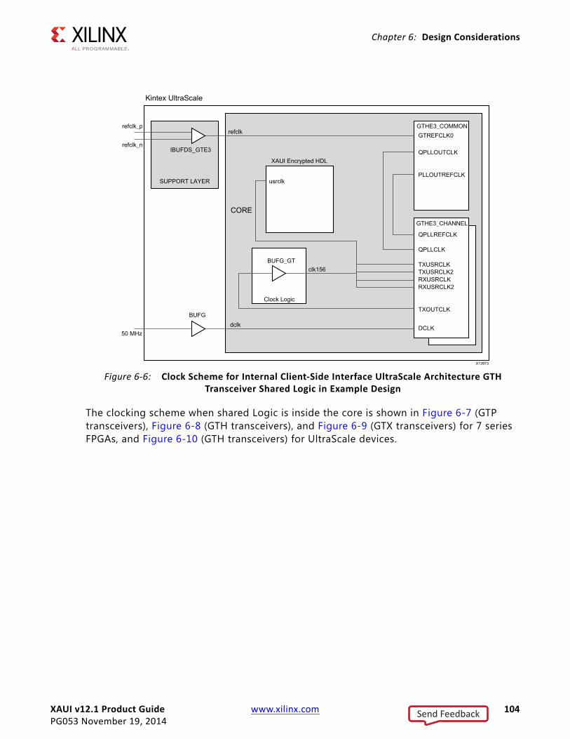
XAUI v12.1 Product Guide www.xilinx.com 104PG053 November 19, 2014
Chapter 6: Design Considerations
The clocking scheme when shared Logic is inside the core is shown in Figure 6-7 (GTP transceivers), Figure 6-8 (GTH transceivers), and Figure 6-9 (GTX transceivers) for 7 series FPGAs, and Figure 6-10 (GTH transceivers) for UltraScale devices.
X-Ref Target - Figure 6-6
Figure 6-6: Clock Scheme for Internal Client-Side Interface UltraScale Architecture GTH Transceiver Shared Logic in Example Design
Send Feedback
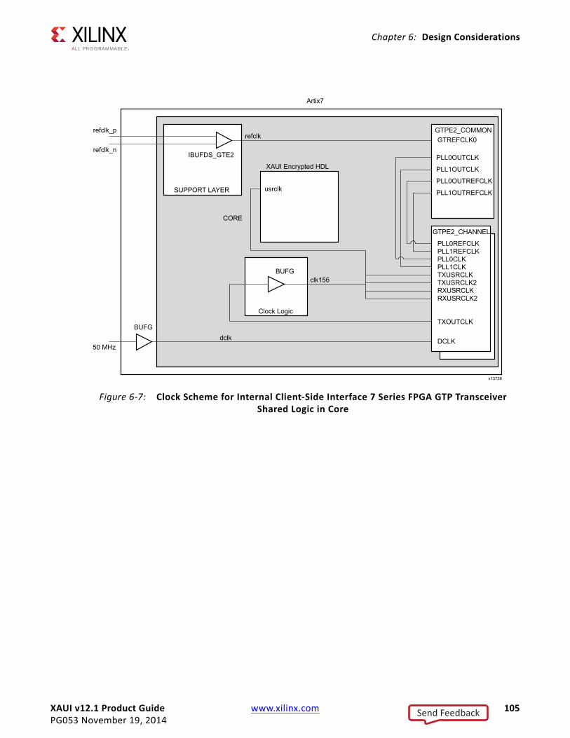
XAUI v12.1 Product Guide www.xilinx.com 105PG053 November 19, 2014
Chapter 6: Design Considerations
X-Ref Target - Figure 6-7
Figure 6-7: Clock Scheme for Internal Client-Side Interface 7 Series FPGA GTP Transceiver Shared Logic in Core
Send Feedback
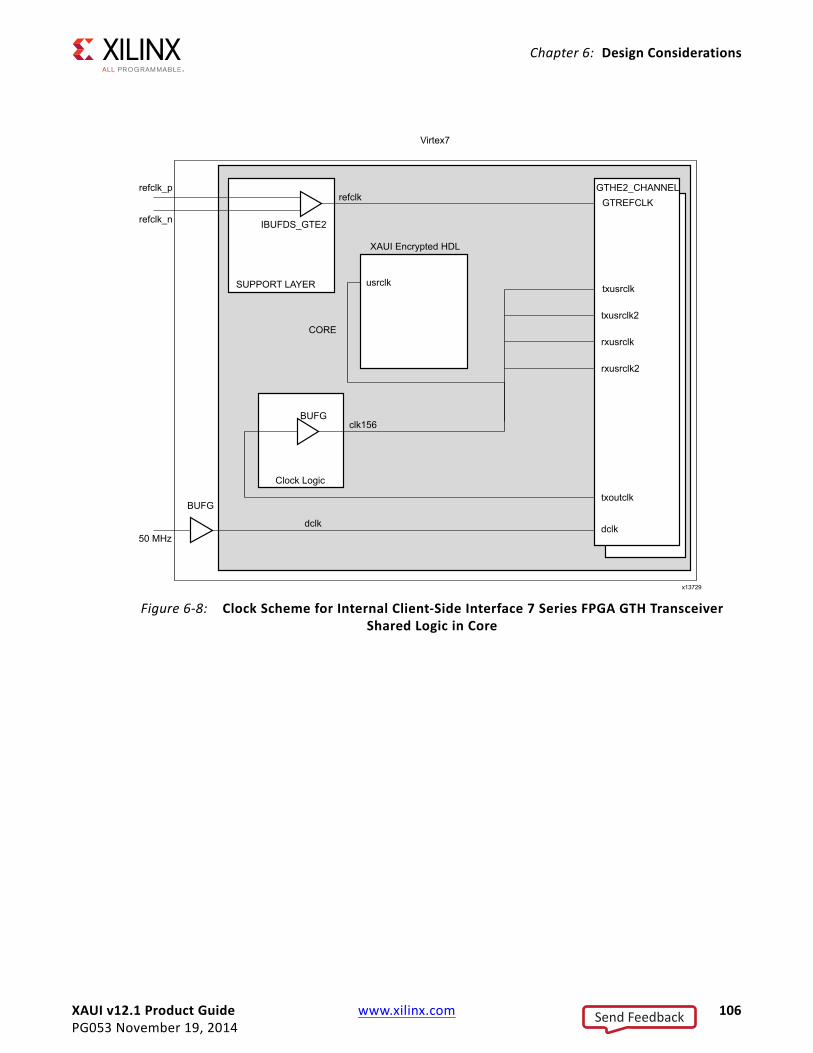
XAUI v12.1 Product Guide www.xilinx.com 106PG053 November 19, 2014
Chapter 6: Design Considerations
X-Ref Target - Figure 6-8
Figure 6-8: Clock Scheme for Internal Client-Side Interface 7 Series FPGA GTH Transceiver Shared Logic in Core
Send Feedback
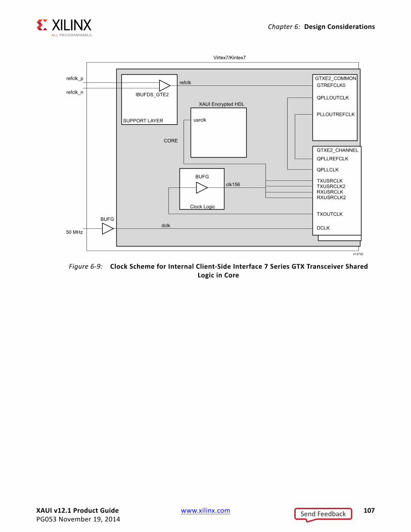
XAUI v12.1 Product Guide www.xilinx.com 107PG053 November 19, 2014
Chapter 6: Design Considerations
X-Ref Target - Figure 6-9
Figure 6-9: Clock Scheme for Internal Client-Side Interface 7 Series GTX Transceiver Shared Logic in Core
Send Feedback
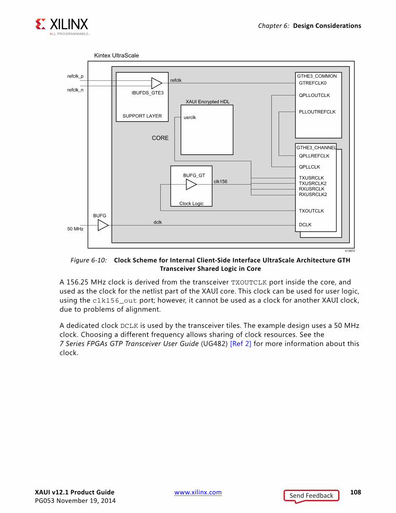
XAUI v12.1 Product Guide www.xilinx.com 108PG053 November 19, 2014
Chapter 6: Design Considerations
A 156.25 MHz clock is derived from the transceiver TXOUTCLK port inside the core, and used as the clock for the netlist part of the XAUI core. This clock can be used for user logic, using the clk156_out port; however, it cannot be used as a clock for another XAUI clock, due to problems of alignment.
A dedicated clock DCLK is used by the transceiver tiles. The example design uses a 50 MHz clock. Choosing a different frequency allows sharing of clock resources. See the 7 Series FPGAs GTP Transceiver User Guide (UG482) [Ref 2] for more information about this clock.
X-Ref Target - Figure 6-10
Figure 6-10: Clock Scheme for Internal Client-Side Interface UltraScale Architecture GTH Transceiver Shared Logic in Core
Send Feedback
XAUI v12.1 Product Guide www.xilinx.com 109PG053 November 19, 2014
Chapter 6: Design Considerations
Internal Client-Side Interface for 20G – XAUI (Zynq-7000, Virtex-7, Kintex-7, Artix-7, and UltraScale Devices) The simplest clocking scheme is the same as in the 10G XAUI.
A 312.5 MHz clock is derived from the transceiver txoutclk port inside the core, and used as the clock for the netlist part of the XAUI core. This clock can be used for user logic, using the clk156_out port; however, it cannot be used as a clock for another XAUI clock, due to problems of alignment.
A dedicated clock is used by the transceiver. The example design uses a 50 MHz clock. Choosing a different frequency allows sharing of clock resources. See the 7 Series FPGAs GTX/GTH Transceiver User Guide (UG476) [Ref 1] and the UltraScale Architecture GTH Transceivers User Guide (UG576) [Ref 3] for more information about this clock.
Multiple Core InstancesIn UltraScale, Virtex®-7 and Kintex®-7 devices, the reference clock can be shared from a neighboring quad. Logic clocks cannot be shared between core instances with the supplied design. The usrclks on each core and quad of transceivers are sourced from the TXOUTCLK port of that quad. See the 7 Series FPGAs GTX/GTH Transceiver User Guide (UG476) [Ref 1] and the UltraScale Architecture GTH Transceivers User Guide (UG576) [Ref 3].
IMPORTANT: The clock from a XAUI core (156.25 MHz or 312.5 MHz) cannot be used by another XAUI core. However, it is possible to use this clock for other user logic.
Reset CircuitsAll register resets within the XAUI core netlist are synchronous to the usrclk port or dclk port, apart from the registers on the input side of the transmit elastic buffer which are synchronous to the tx_clk port.
Receiver Termination: Virtex-7 and Kintex-7 FPGAsThe receiver termination must be set correctly. The default setting is 2/3 VTTRX. See the Receiver chapter in the 7 Series FPGAs GTX/GTH Transceiver User Guide (UG476) [Ref 1].
Send Feedback
XAUI v12.1 Product Guide www.xilinx.com 110PG053 November 19, 2014
Chapter 6: Design Considerations
Transmit SkewThe transceivers are configured to operate in a mode that minimizes the amount of transmit skew that can be introduced between lanes. Full details on that maximum amount of transmit skew can be found by looking at TLLSKEW in the appropriate device data sheet.
Under some circumstances it is possible that TLLSKEW can exceed the PMA Tx Skew budget defined in 802.3-2012. If it is necessary to keep within this skew budget, then the appropriate amount must be borrowed from the PCB and medium sections of the budget to keep the total amount of skew within range.
Send Feedback
XAUI v12.1 Product Guide www.xilinx.com 111PG053 November 19, 2014
Chapter 7
Design Flow StepsThis chapter describes customizing and generating the core, constraining the core, and the simulation, synthesis and implementation steps that are specific to this IP core. More detailed information about the standard Vivado® design flows in the IP Integrator can be found in the following Vivado Design Suite user guides:
• Vivado Design Suite User Guide: Designing IP Subsystems using IP Integrator (UG994) [Ref 10]
• Vivado Design Suite User Guide: Designing with IP (UG896) [Ref 4]
• Vivado Design Suite User Guide: Getting Started (UG910) [Ref 5]
• Vivado Design Suite User Guide: Logic Simulation (UG900) [Ref 6]
Customizing and Generating the CoreYou can customize the IP for use in your design by specifying values for the various parameters associated with the IP core using the following steps:
1. Select the IP from the IP catalog.
2. Double-click the selected IP or select the Customize IP command from the toolbar or popup menu.
For details, see the Vivado Design Suite User Guide: Designing with IP (UG896) [Ref 4] and the Vivado Design Suite User Guide: Getting Started (UG910) [Ref 5].
Note: Figures in this chapter are illustrations of the Vivado IDE. This layout might vary from the current version.
Send Feedback
XAUI v12.1 Product Guide www.xilinx.com 112PG053 November 19, 2014
Chapter 7: Design Flow Steps
Main Screen
Component NameEnter the desired name for the core.
Data RateSelects between 10G and 20G XAUI Data Rates.
MDIO ManagementUse the MDIO Management interface or configuration/status vectors.
Transceiver Control and Status Ports
If selected, enables additional transceiver control ports for DRP, Tx Driver, Rx Equalization, and other features such as PRBS.
X-Ref Target - Figure 7-1
Figure 7-1: Main Screen
Send Feedback
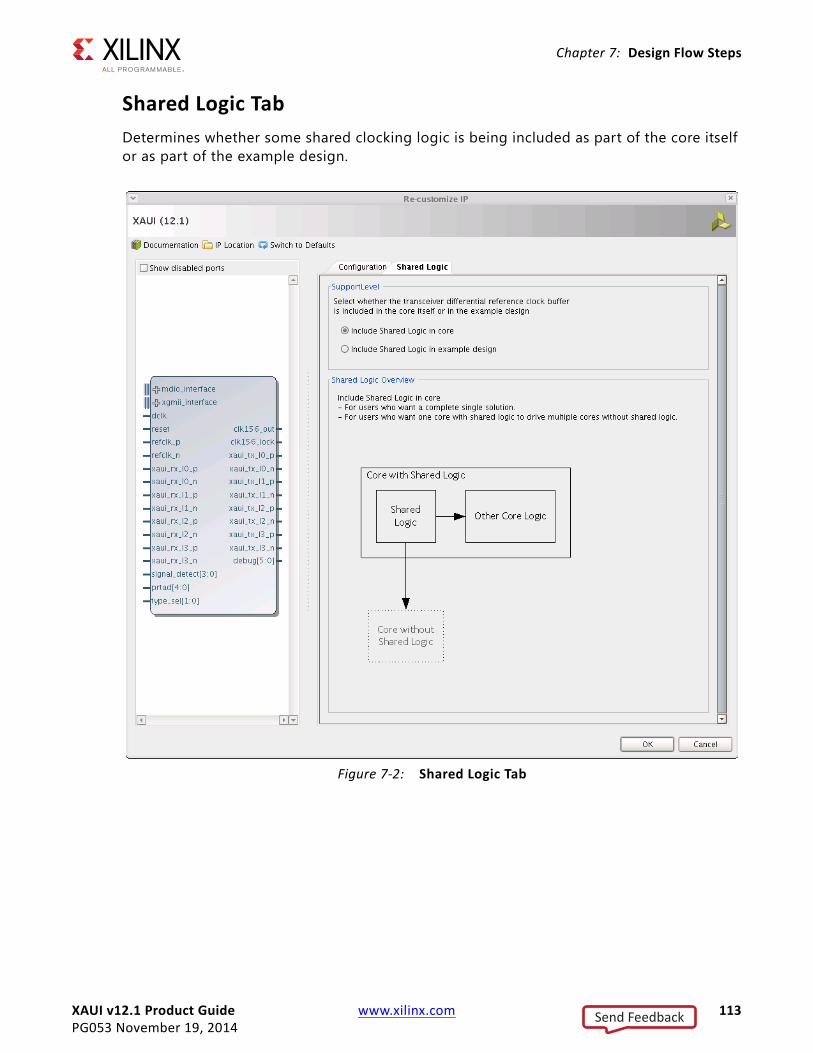
XAUI v12.1 Product Guide www.xilinx.com 113PG053 November 19, 2014
Chapter 7: Design Flow Steps
Shared Logic TabDetermines whether some shared clocking logic is being included as part of the core itself or as part of the example design.
X-Ref Target - Figure 7-2
Figure 7-2: Shared Logic Tab
Send Feedback
XAUI v12.1 Product Guide www.xilinx.com 114PG053 November 19, 2014
Chapter 7: Design Flow Steps
User ParametersTable 7-1 shows the relationship between the GUI f ields in the Vivado IDE and the User Parameters (which can be viewed in the Tcl console).
Output GenerationFor details, see “Generating IP Output Products” in the Vivado Design Suite User Guide: Designing with IP (UG896) [Ref 4].
Constraining the CoreThis section contains information about constraining the core in the Vivado Design Suite.
Required ConstraintsThis section defines the constraint requirements for the core. Constraints are provided with an XDC file. An XDC is provided with the HDL example design to give a starting point for constraints for the user design. The following constraints are required.
Constraints specific to the core are applied by the Vivado® Design Suite. A hierarchical XDC is applied to the core that will apply the necessary clock constraints. System-level constraints such as DCLK frequency and Transceiver location should be applied in the user XDC.
Table 7-1: GUI Parameter to User Parameter RelationshipGUI Parameter/Value(1) User Parameter/Value(1) Default Value
MDIO Management Mdio_Management true
Data Rate Data_Rate TenGbps
TenGbps TenGbps
TwentyGbps TwentyGbps
Shared Logic SupportLevel 0
Include Shared Logic in core 1
Include Shared Logic in example design
0
Additional transceiver control and status ports
TransceiverControl false
1. Parameter values are listed in the table where the GUI parameter value differs from the user parameter value. Such values are shown in this table as indented below the associated parameter.
Send Feedback
XAUI v12.1 Product Guide www.xilinx.com 115PG053 November 19, 2014
Chapter 7: Design Flow Steps
Clock FrequenciesA constraint specifying the frequency of the clock (156.25 MHz for 10G or 312.5 MHz for 20G) is already set in the hierarchical XDC file. This clock is being sourced from the txoutclk port of one of the transceivers inside the core.
DCLK clock must be provided and a constraint is required to specify its frequency:
create_clock -name dclk -period 20.000 [get_ports dclk]
Transceiver Placement
7-Series Devices
Transceivers should be given location constraints appropriate to your design for 7 series devices. The following example illustrates GTX transceivers:
set_property LOC GTXE2_CHANNEL_X1Y8 [get_cells -hierarchical -filter {NAME =~ */gt_wrapper_i/gt0_<CompName>_gt_wrapper_i/gtxe2_i}]set_property LOC GTXE2_CHANNEL_X1Y9 [get_cells -hierarchical -filter {NAME =~ */gt_wrapper_i/gt1_<CompName>_gt_wrapper_i/gtxe2_i}]set_property LOC GTXE2_CHANNEL_X1Y10 [get_cells -hierarchical -filter {NAME =~ */gt_wrapper_i/gt2_<CompName>_gt_wrapper_i/gtxe2_i}]set_property LOC GTXE2_CHANNEL_X1Y11 [get_cells -hierarchical -filter {NAME =~ */gt_wrapper_i/gt3_<CompName>_gt_wrapper_i/gtxe2_i}]
For GTH transceivers: replace the GTXE2 string with GTHE2 and the gtxe2_i string with gthe2_i, and change the X/Y coordinates to your chosen location.
For Artix-7 GTP transceivers: replace the GTXE2 string with GTPE2 and the gthe2_i string with gtpe2_i, and change the X/Y coordinates to your chosen location.
UltrasScale Devices
The following example illustrates the placement of GHTE3 transceivers when the shared logic is in the example design:
set_property LOC GTHE3_CHANNEL_X0Y0 [get_cells xaui_support_i/xaui_i/inst/<=: CompName :>_gt_i/*/gen_gtwizard_gthe3_top.<CompName>_gt_gtwizard_gthe3_inst/gen_gtwizard_gthe3.gen_channel_container[*].gen_enabled_channel.gthe3_channel_wrapper_inst/channel_inst/gthe3_channel_gen.gen_gthe3_channel_inst[0].GTHE3_CHANNEL_PRIM_INST ]set_property LOC GTHE3_CHANNEL_X0Y1 [get_cells xaui_support_i/xaui_i/inst/<=: CompName :>_gt_i/*/gen_gtwizard_gthe3_top.<=: CompName :>_gt_gtwizard_gthe3_inst/gen_gtwizard_gthe3.gen_channel_container[*].gen_enabled_channel.gthe3_channel_wrapper_inst/channel_inst/gthe3_channel_gen.gen_gthe3_channel_inst[1].GTHE3_CHANNEL_PRIM_INST ]set_property LOC GTHE3_CHANNEL_X0Y2 [get_cells xaui_support_i/xaui_i/inst/<=: CompName :>_gt_i/*/gen_gtwizard_gthe3_top.<=: CompName :>_gt_gtwizard_gthe3_inst/gen_gtwizard_gthe3.gen_channel_container[*].gen_enabled_channel.gthe3_channel_wrapper_inst/channel_inst/gthe3_channel_gen.gen_gthe3_channel_inst[2].GTHE3_CHANNEL_PRIM_INST ]
Send Feedback
XAUI v12.1 Product Guide www.xilinx.com 116PG053 November 19, 2014
Chapter 7: Design Flow Steps
set_property LOC GTHE3_CHANNEL_X0Y3 [get_cells xaui_support_i/xaui_i/inst/<=: CompName :>_gt_i/*/gen_gtwizard_gthe3_top.<=: CompName :>_gt_gtwizard_gthe3_inst/gen_gtwizard_gthe3.gen_channel_container[*].gen_enabled_channel.gthe3_channel_wrapper_inst/channel_inst/gthe3_channel_gen.gen_gthe3_channel_inst[3].GTHE3_CHANNEL_PRIM_INST ]set_property LOC GTHE3_COMMON_X0Y0 [get_cells xaui_support_i/xaui_i/*/<=: CompName :>_gt_i/inst/gen_gtwizard_gthe3_top.<=: CompName :>_gt_gtwizard_gthe3_inst/gen_gtwizard_gthe3.gen_common.gen_common_container[*].gen_enabled_common.gthe3_common_wrapper_inst/common_inst/gthe3_common_gen.GTHE3_COMMON_PRIM_INST ]
When shared logic is in the core, the GTHE3 transceivers can be placed using the following example:
set_property LOC GTHE3_CHANNEL_X0Y0 [get_cells xaui_i/inst/xaui_block_i/<=: CompName :>_gt_i/*/gen_gtwizard_gthe3_top.<=: CompName :>_gt_gtwizard_gthe3_inst/gen_gtwizard_gthe3.gen_channel_container[*].gen_enabled_channel.gthe3_channel_wrapper_inst/channel_inst/gthe3_channel_gen.gen_gthe3_channel_inst[0].GTHE3_CHANNEL_PRIM_INST ]set_property LOC GTHE3_CHANNEL_X0Y1 [get_cells xaui_i/inst/xaui_block_i/<=: CompName :>_gt_i/*/gen_gtwizard_gthe3_top.<=: CompName :>_gt_gtwizard_gthe3_inst/gen_gtwizard_gthe3.gen_channel_container[*].gen_enabled_channel.gthe3_channel_wrapper_inst/channel_inst/gthe3_channel_gen.gen_gthe3_channel_inst[1].GTHE3_CHANNEL_PRIM_INST ]set_property LOC GTHE3_CHANNEL_X0Y2 [get_cells xaui_i/inst/xaui_block_i/<=: CompName :>_gt_i/*/gen_gtwizard_gthe3_top.<=: CompName :>_gt_gtwizard_gthe3_inst/gen_gtwizard_gthe3.gen_channel_container[*].gen_enabled_channel.gthe3_channel_wrapper_inst/channel_inst/gthe3_channel_gen.gen_gthe3_channel_inst[2].GTHE3_CHANNEL_PRIM_INST ]set_property LOC GTHE3_CHANNEL_X0Y3 [get_cells xaui_i/inst/xaui_block_i/<=: CompName :>_gt_i/*/gen_gtwizard_gthe3_top.<=: CompName :>_gt_gtwizard_gthe3_inst/gen_gtwizard_gthe3.gen_channel_container[*].gen_enabled_channel.gthe3_channel_wrapper_inst/channel_inst/gthe3_channel_gen.gen_gthe3_channel_inst[3].GTHE3_CHANNEL_PRIM_INST ]set_property LOC GTHE3_COMMON_X0Y0 [get_cells xaui_i/*/xaui_block_i/<=: CompName :>_gt_i/inst/gen_gtwizard_gthe3_top.<=: CompName :>_gt_gtwizard_gthe3_inst/gen_gtwizard_gthe3.gen_common.gen_common_container[*].gen_enabled_common.gthe3_common_wrapper_inst/common_inst/gthe3_common_gen.GTHE3_COMMON_PRIM_INST ]
SimulationFor comprehensive information about Vivado® simulation components, as well as information about using supported third-party tools, see the Vivado Design Suite User Guide: Logic Simulation (UG900) [Ref 6].
All simulation sources are included that are required by the core. Simulation of XAUI at the core level is not supported without the addition of a test bench (not supplied). Simulation of the example design is supported.
Send Feedback
XAUI v12.1 Product Guide www.xilinx.com 117PG053 November 19, 2014
Chapter 7: Design Flow Steps
Synthesis and ImplementationFor details about synthesis and implementation, see “Synthesizing IP” and “Implementing IP” in the Vivado Design Suite User Guide: Designing with IP (UG896) [Ref 4].
All synthesis sources are included that are required by the core. For the XAUI core this is a mix of both encrypted and unencrypted source. Only the unencrypted sources are visible and optionally editable by using the Unlink IP Vivado option.
Send Feedback
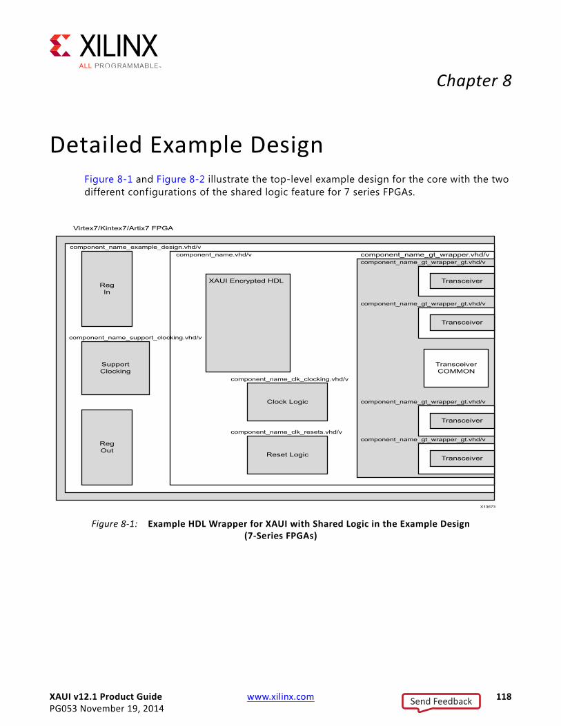
XAUI v12.1 Product Guide www.xilinx.com 118PG053 November 19, 2014
Chapter 8
Detailed Example DesignFigure 8-1 and Figure 8-2 illustrate the top-level example design for the core with the two different configurations of the shared logic feature for 7 series FPGAs.
X-Ref Target - Figure 8-1
Figure 8-1: Example HDL Wrapper for XAUI with Shared Logic in the Example Design (7-Series FPGAs)
Send Feedback
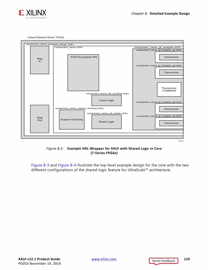
XAUI v12.1 Product Guide www.xilinx.com 119PG053 November 19, 2014
Chapter 8: Detailed Example Design
Figure 8-3 and Figure 8-4 illustrate the top-level example design for the core with the two different configurations of the shared logic feature for UltraScale™ architecture.
X-Ref Target - Figure 8-2
Figure 8-2: Example HDL Wrapper for XAUI with Shared Logic in Core(7-Series FPGAs)
Send Feedback
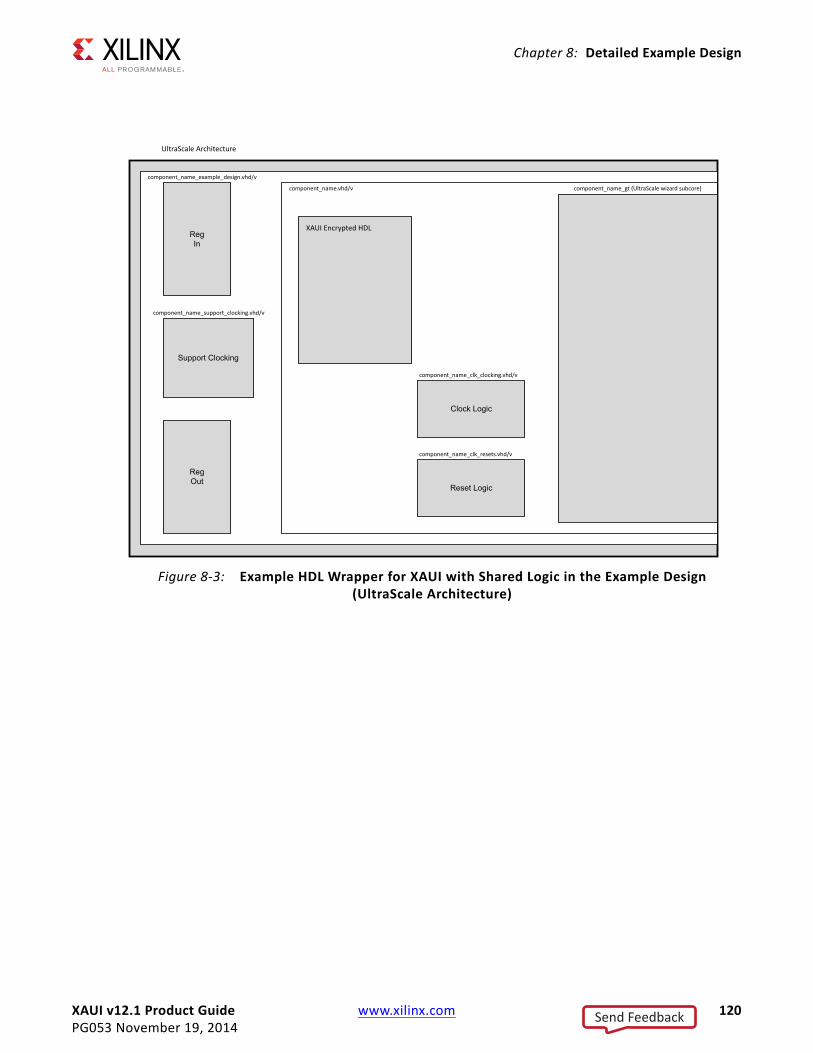
XAUI v12.1 Product Guide www.xilinx.com 120PG053 November 19, 2014
Chapter 8: Detailed Example Design
X-Ref Target - Figure 8-3
Figure 8-3: Example HDL Wrapper for XAUI with Shared Logic in the Example Design (UltraScale Architecture)
Send Feedback
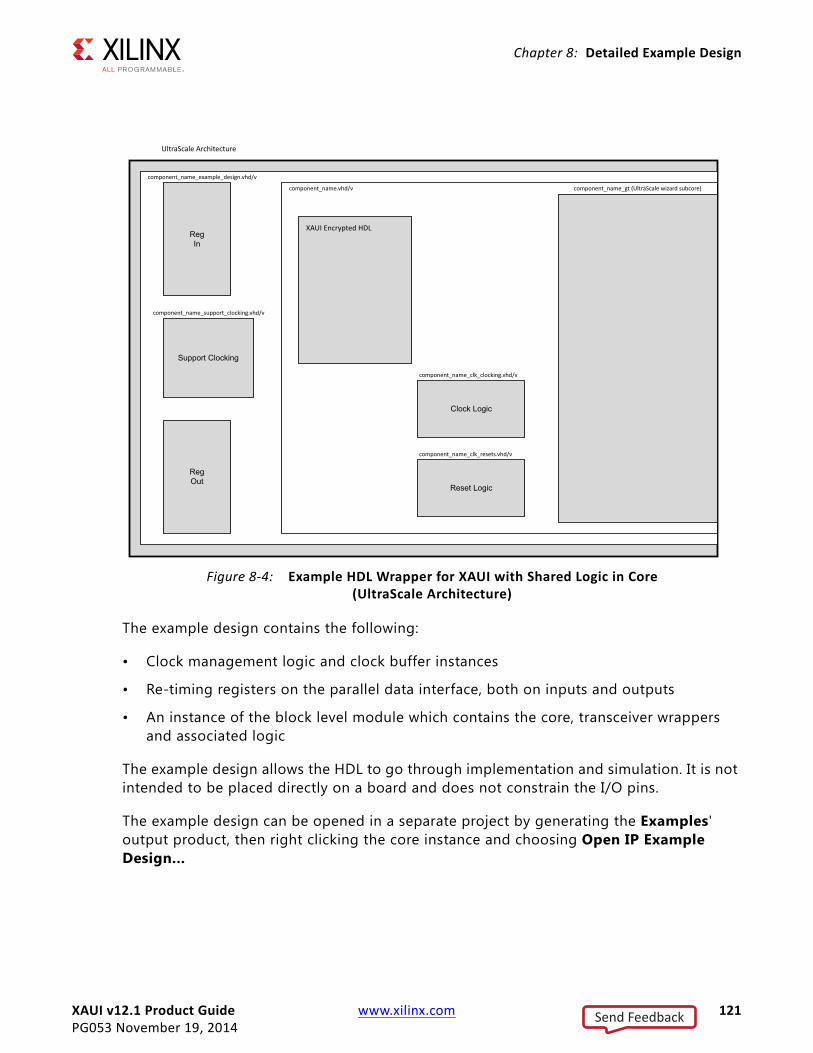
XAUI v12.1 Product Guide www.xilinx.com 121PG053 November 19, 2014
Chapter 8: Detailed Example Design
The example design contains the following:
• Clock management logic and clock buffer instances
• Re-timing registers on the parallel data interface, both on inputs and outputs
• An instance of the block level module which contains the core, transceiver wrappers and associated logic
The example design allows the HDL to go through implementation and simulation. It is not intended to be placed directly on a board and does not constrain the I/O pins.
The example design can be opened in a separate project by generating the Examples' output product, then right clicking the core instance and choosing Open IP Example Design...
X-Ref Target - Figure 8-4
Figure 8-4: Example HDL Wrapper for XAUI with Shared Logic in Core (UltraScale Architecture)
Send Feedback
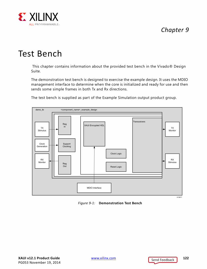
XAUI v12.1 Product Guide www.xilinx.com 122PG053 November 19, 2014
Chapter 9
Test Bench This chapter contains information about the provided test bench in the Vivado® Design Suite.
The demonstration test bench is designed to exercise the example design. It uses the MDIO management interface to determine when the core is initialized and ready for use and then sends some simple frames in both Tx and Rx directions.
The test bench is supplied as part of the Example Simulation output product group.
X-Ref Target - Figure 9-1
Figure 9-1: Demonstration Test Bench
Send Feedback
XAUI v12.1 Product Guide www.xilinx.com 123PG053 November 19, 2014
Chapter 9: Test Bench
The demonstration test bench is defined in the demo_tb.v/vhd f ile.
The test bench, shown in Figure 9-1 consists of:
• Clock generators
• A TX stimulus block
• A RX stimulus block
• A TX Monitor block, which checks that transmission was made successfully
• A RX Monitor block, which checks that reception was made successfully
• A MDIO monitor to check when the core is ready to send/receive frames
The demonstration test bench performs the following tasks:
• Clocks are generated.
• An initial reset is applied.
• The MDIO interface is addressed to check when the XAUI core is ready to send/receive frames.
• When the core is ready, the TX/RX stimulus blocks send four frames.
• The RX/TX Monitor blocks check the resulting frames against the original ones.
• A watchdog timer is set to stop the simulation with a failure after 200 µs for GTX and GTH (20G XAUI) or 3 ms for GTP and GTH (10G XAUI) transceivers and 800 µs for UltraScale™ devices.
Send Feedback
XAUI v12.1 Product Guide www.xilinx.com 124PG053 November 19, 2014
Appendix A
Verification and InteroperabilityThe XAUI core has been verif ied using both simulation and hardware testing.
SimulationA highly parameterizable transaction-based simulation test suite has been used to verify the core. Tests included:
• Register access over MDIO
• Loss and re-gain of synchronization
• Loss and re-gain of alignment
• Frame transmission
• Frame reception
• Clock compensation
• Recovery from error conditions
Hardware TestingThe core has been used in several hardware test platforms within Xilinx. In particular, the core has been used in a test platform design with the Xilinx® 10-Gigabit Ethernet MAC core. This design comprises the MAC, XAUI, a “ping” loopback FIFO, and a test pattern generator all under embedded PowerPC® processor control. This design has been used for conformance and interoperability testing at the University of New Hampshire Interoperability Lab. PCS reports are available from the factory on request.
Send Feedback
XAUI v12.1 Product Guide www.xilinx.com 125PG053 November 19, 2014
Appendix B
Migrating and UpgradingThis appendix contains information about migrating a design from ISE® to the Vivado® Design Suite, and for upgrading to a more recent version of the IP core. For customers upgrading in the Vivado Design Suite, important details (where applicable) about any port changes and other impact to user logic are included.
Device MigrationIf you are migrating from a 7 series GTX or GTH device to an UltraScale GTH device, the prefixes of the optional transceiver debug ports for single-lane cores are changed from “gt0”, “gt1” to “gt”, and the suff ix “_in” and “_out” are dropped. For multi-lane cores, the prefixes of the optional transceiver debug ports gt(n) are aggregated into a single port. For example: gt0_gtrxreset and gt1_gtrxreset now become gt_gtrxreset [1:0]. This is true for all ports, with the exception of the DRP buses which follow the convention of gt(n)_drpxyz.
It is important to update your design to use the new transceiver debug port names. For more information about migration to UltraScale devices, see the UltraScale Architecture Migration Methodology Guide (UG1026) [Ref 7].
Migrating to the Vivado Design SuiteFor information on migrating from ISE tools to the Vivado Design Suite, see the ISE to Vivado Design Suite Migration Guide (UG911) [Ref 8].
Upgrading in the Vivado Design SuiteIn the latest revision of the core, there have been several changes that make the core pin-incompatible with the previous version(s) due to the addition of certain features such as shared logic, the transceiver control and status port and the generation of clock and reset internally inside the core.
Send Feedback
XAUI v12.1 Product Guide www.xilinx.com 126PG053 November 19, 2014
Appendix B: Migrating and Upgrading
Parameter ChangesThere have been no parameter changes from v11.0.
Port Changes From v11.0 to v12.1In v11.0, the 156.25 MHz clock was previously an input port (clk156), usually generated using the txoutclk port from the transceiver. In v12.0, the clock generation is done internally inside the actual core; therefore, removing the need for the input port clk156 and the output port txoutclk . Additionally, the core in v12.0 provides the port clk156_out in order to share this clock with the user logic (However, note that this clock should not be used to drive another XAUI core).
Because of the internal clock generation, the port mmcm_lock is no longer required. Also, the output port txlock has changed its name to clk156_lock .
The synchronous reset was also an input in v11.0 and now it is generated inside the core in v12.0. For this reason, input port reset156 is no longer required.
In v12.0, mgt_tx_ready, align_status, and sync_status ports have been grouped into a single debug port.
The ports related to the drp interface (drp_addr, drp_en, drp_i, drp_o, drp_rdy, drp_we) are now split into four sets, one for each transceiver, and are only available when the Transceiver Control and Status Ports option is enabled, receiving the names:
• Channel 0: gt0_drpaddr, gt0_drpen, gt0_drpdi, gt0_drpdo, gt0_drprdy, and gt0_drpwe;
• Channel 1: gt1_drpaddr, gt1_drpen, gt1_drpdi, gt1_drpdo, gt1_drprdy, and gt1_drpwe0;
• Channel 2: gt2_drpaddr, gt2_drpen, gt2_drpdi, gt2_drpdo, gt2_drprdy, and gt2_drpwe;
• Channel 3: gt3_drpaddr, gt3_drpen, gt3_drpdi, gt3_drpdo, gt3_drprdy, and gt3_drpwe
If the Transceiver Control and Status Ports option is enabled, the core also provides some extra ports, which have already been described in Table 2-8.
Send Feedback
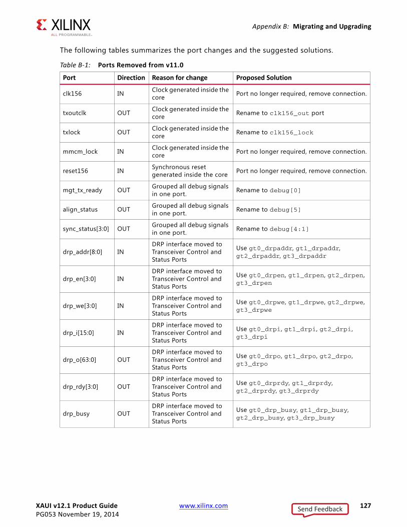
XAUI v12.1 Product Guide www.xilinx.com 127PG053 November 19, 2014
Appendix B: Migrating and Upgrading
The following tables summarizes the port changes and the suggested solutions.
Table B-1: Ports Removed from v11.0
Port Direction Reason for change Proposed Solution
clk156 IN Clock generated inside the core Port no longer required, remove connection.
txoutclk OUT Clock generated inside the core Rename to clk156_out port
txlock OUT Clock generated inside the core Rename to clk156_lock
mmcm_lock IN Clock generated inside the core Port no longer required, remove connection.
reset156 IN Synchronous reset generated inside the core Port no longer required, remove connection.
mgt_tx_ready OUT Grouped all debug signals in one port. Rename to debug[0]
align_status OUT Grouped all debug signals in one port. Rename to debug[5]
sync_status[3:0] OUT Grouped all debug signals in one port. Rename to debug[4:1]
drp_addr[8:0] INDRP interface moved to Transceiver Control and Status Ports
Use gt0_drpaddr, gt1_drpaddr, gt2_drpaddr, gt3_drpaddr
drp_en[3:0] INDRP interface moved to Transceiver Control and Status Ports
Use gt0_drpen, gt1_drpen, gt2_drpen, gt3_drpen
drp_we[3:0] INDRP interface moved to Transceiver Control and Status Ports
Use gt0_drpwe, gt1_drpwe, gt2_drpwe, gt3_drpwe
drp_i[15:0] INDRP interface moved to Transceiver Control and Status Ports
Use gt0_drpi, gt1_drpi, gt2_drpi, gt3_drpi
drp_o[63:0] OUTDRP interface moved to Transceiver Control and Status Ports
Use gt0_drpo, gt1_drpo, gt2_drpo, gt3_drpo
drp_rdy[3:0] OUTDRP interface moved to Transceiver Control and Status Ports
Use gt0_drprdy, gt1_drprdy, gt2_drprdy, gt3_drprdy
drp_busy OUTDRP interface moved to Transceiver Control and Status Ports
Use gt0_drp_busy, gt1_drp_busy, gt2_drp_busy, gt3_drp_busy
Send Feedback
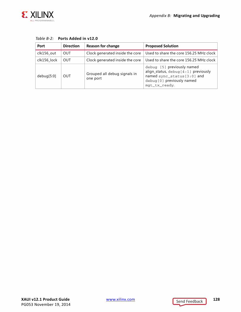
XAUI v12.1 Product Guide www.xilinx.com 128PG053 November 19, 2014
Appendix B: Migrating and Upgrading
Table B-2: Ports Added in v12.0
Port Direction Reason for change Proposed Solution
clk156_out OUT Clock generated inside the core Used to share the core 156.25 MHz clock
clk156_lock OUT Clock generated inside the core Used to share the core 156.25 MHz clock
debug[5:0] OUT Grouped all debug signals in one port
debug [5] previously named align_status, debug[4:1] previously named sync_status[3:0] and debug[0] previously named mgt_tx_ready.
Send Feedback
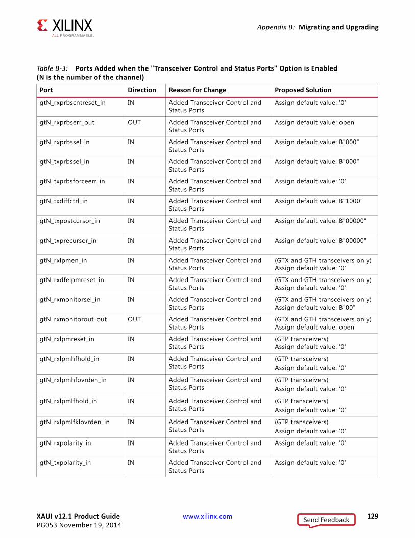
XAUI v12.1 Product Guide www.xilinx.com 129PG053 November 19, 2014
Appendix B: Migrating and Upgrading
Table B-3: Ports Added when the "Transceiver Control and Status Ports" Option is Enabled (N is the number of the channel)
Port Direction Reason for Change Proposed Solution
gtN_rxprbscntreset_in IN Added Transceiver Control and Status Ports
Assign default value: '0'
gtN_rxprbserr_out OUT Added Transceiver Control and Status Ports
Assign default value: open
gtN_rxprbssel_in IN Added Transceiver Control and Status Ports
Assign default value: B"000"
gtN_txprbssel_in IN Added Transceiver Control and Status Ports
Assign default value: B"000"
gtN_txprbsforceerr_in IN Added Transceiver Control and Status Ports
Assign default value: '0'
gtN_txdiffctrl_in IN Added Transceiver Control and Status Ports
Assign default value: B"1000"
gtN_txpostcursor_in IN Added Transceiver Control and Status Ports
Assign default value: B"00000"
gtN_txprecursor_in IN Added Transceiver Control and Status Ports
Assign default value: B"00000"
gtN_rxlpmen_in IN Added Transceiver Control and Status Ports
(GTX and GTH transceivers only) Assign default value: '0'
gtN_rxdfelpmreset_in IN Added Transceiver Control and Status Ports
(GTX and GTH transceivers only) Assign default value: '0'
gtN_rxmonitorsel_in IN Added Transceiver Control and Status Ports
(GTX and GTH transceivers only) Assign default value: B"00"
gtN_rxmonitorout_out OUT Added Transceiver Control and Status Ports
(GTX and GTH transceivers only) Assign default value: open
gtN_rxlpmreset_in IN Added Transceiver Control and Status Ports
(GTP transceivers) Assign default value: '0'
gtN_rxlpmhfhold_in IN Added Transceiver Control and Status Ports
(GTP transceivers) Assign default value: '0'
gtN_rxlpmhfovrden_in IN Added Transceiver Control and Status Ports
(GTP transceivers) Assign default value: '0'
gtN_rxlpmlfhold_in IN Added Transceiver Control and Status Ports
(GTP transceivers) Assign default value: '0'
gtN_rxlpmlfklovrden_in IN Added Transceiver Control and Status Ports
(GTP transceivers) Assign default value: '0'
gtN_rxpolarity_in IN Added Transceiver Control and Status Ports
Assign default value: '0'
gtN_txpolarity_in IN Added Transceiver Control and Status Ports
Assign default value: '0'
Send Feedback
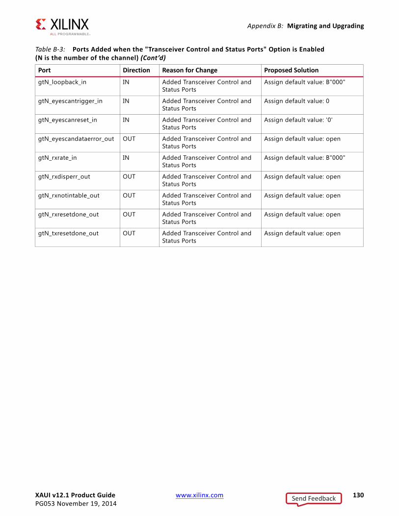
XAUI v12.1 Product Guide www.xilinx.com 130PG053 November 19, 2014
Appendix B: Migrating and Upgrading
gtN_loopback_in IN Added Transceiver Control and Status Ports
Assign default value: B"000"
gtN_eyescantrigger_in IN Added Transceiver Control and Status Ports
Assign default value: 0
gtN_eyescanreset_in IN Added Transceiver Control and Status Ports
Assign default value: '0'
gtN_eyescandataerror_out OUT Added Transceiver Control and Status Ports
Assign default value: open
gtN_rxrate_in IN Added Transceiver Control and Status Ports
Assign default value: B"000"
gtN_rxdisperr_out OUT Added Transceiver Control and Status Ports
Assign default value: open
gtN_rxnotintable_out OUT Added Transceiver Control and Status Ports
Assign default value: open
gtN_rxresetdone_out OUT Added Transceiver Control and Status Ports
Assign default value: open
gtN_txresetdone_out OUT Added Transceiver Control and Status Ports
Assign default value: open
Table B-3: Ports Added when the "Transceiver Control and Status Ports" Option is Enabled (N is the number of the channel) (Cont’d)
Port Direction Reason for Change Proposed Solution
Send Feedback
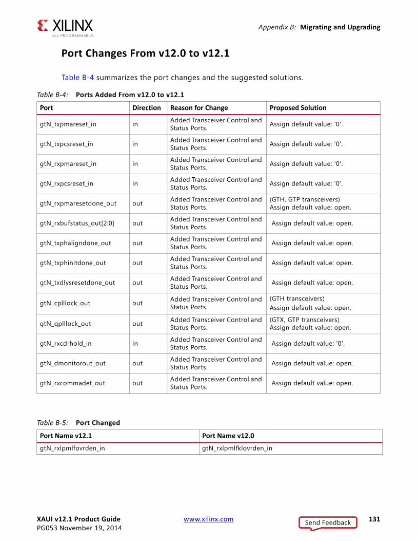
XAUI v12.1 Product Guide www.xilinx.com 131PG053 November 19, 2014
Appendix B: Migrating and Upgrading
Port Changes From v12.0 to v12.1
Table B-4 summarizes the port changes and the suggested solutions.
Table B-4: Ports Added From v12.0 to v12.1
Port Direction Reason for Change Proposed Solution
gtN_txpmareset_in in Added Transceiver Control and Status Ports. Assign default value: '0'.
gtN_txpcsreset_in in Added Transceiver Control and Status Ports. Assign default value: '0'.
gtN_rxpmareset_in in Added Transceiver Control and Status Ports. Assign default value: '0'.
gtN_rxpcsreset_in in Added Transceiver Control and Status Ports. Assign default value: '0'.
gtN_rxpmaresetdone_out out Added Transceiver Control and Status Ports.
(GTH, GTP transceivers) Assign default value: open.
gtN_rxbufstatus_out[2:0] out Added Transceiver Control and Status Ports. Assign default value: open.
gtN_txphaligndone_out out Added Transceiver Control and Status Ports. Assign default value: open.
gtN_txphinitdone_out out Added Transceiver Control and Status Ports. Assign default value: open.
gtN_txdlysresetdone_out out Added Transceiver Control and Status Ports. Assign default value: open.
gtN_cplllock_out out Added Transceiver Control and Status Ports.
(GTH transceivers) Assign default value: open.
gtN_qplllock_out out Added Transceiver Control and Status Ports.
(GTX, GTP transceivers) Assign default value: open.
gtN_rxcdrhold_in in Added Transceiver Control and Status Ports. Assign default value: '0'.
gtN_dmonitorout_out out Added Transceiver Control and Status Ports. Assign default value: open.
gtN_rxcommadet_out out Added Transceiver Control and Status Ports. Assign default value: open.
Table B-5: Port Changed
Port Name v12.1 Port Name v12.0
gtN_rxlpmlfovrden_in gtN_rxlpmlfklovrden_in
Send Feedback
XAUI v12.1 Product Guide www.xilinx.com 132PG053 November 19, 2014
Appendix C
Debugging DesignsThis chapter provides information on using resources available on the Xilinx® Support website, available debug tools, and a step-by-step process for debugging designs that use the XAUI core.
Finding Help on xilinx.comTo help in the design and debug process when using the XAUI core, the Xilinx Support web page (www.xilinx.com/support) contains key resources such as product documentation, release notes, answer records, and links for obtaining further product support.
DocumentationThis product guide is the main document associated with the XAUI core. This guide, along with documentation related to all products that aid in the design process, can be found on the Xilinx Support web page (www.xilinx.com/support) or by using the Xilinx Documentation Navigator.
Download the Xilinx Documentation Navigator from the Design Tools tab on the Downloads page (www.xilinx.com/download). For more information about this tool and the features available, open the online help after installation.
Send Feedback
XAUI v12.1 Product Guide www.xilinx.com 133PG053 November 19, 2014
Appendix C: Debugging Designs
Answer RecordsAnswer Records include information on commonly encountered problems, helpful information on how to resolve these problems, and any known issues with a Xilinx product. Answer Records are created and maintained daily ensuring that users have access to the most up-to-date information on Xilinx products.
Answer Records can be found by searching the Answers Database.
To use the Answers Database Search:
1. Navigate to www.xilinx.com/support. The Answers Database Search is located at top of this web page.
2. Enter keywords in the provided search f ield and select Search.
• Examples of searchable keywords are product names, error messages, or a generic summary of the issue encountered.
• To see all answer records directly related to the XAUI core, search for the phrase "XAUI."
Master Answer Record for the XAUI core
AR 54666
Contacting Technical SupportXilinx provides technical support at www.xilinx.com/support for this LogiCORE™ IP product when used as described in the product documentation. Xilinx cannot guarantee timing, functionality, or support of product if implemented in devices that are not defined in the documentation, if customized beyond that allowed in the product documentation, or if changes are made to any section of the design labeled DO NOT MODIFY.
To contact Technical Support:
1. Navigate to www.xilinx.com/support.
2. Open a WebCase by selecting the WebCase link located under Additional Resources.
When opening a WebCase, include:
• Target FPGA including package and speed grade.
• All applicable Xilinx Design Tools and simulator software versions.
• Additional f iles based on the specif ic issue might also be required. See the relevant sections in this debug guide for guidelines about which f ile(s) to include with the WebCase.
Send Feedback
XAUI v12.1 Product Guide www.xilinx.com 134PG053 November 19, 2014
Appendix C: Debugging Designs
Note: Access to WebCase is not available in all cases. Login to the WebCase tool to see your specif ic support options.
Debug Tools
Vivado Lab ToolsVivado® lab tools insert logic analyzer and virtual I/O cores directly into your design. Vivado lab tools allow you to set trigger conditions to capture application and integrated block port signals in hardware. Captured signals can then be analyzed. This feature represents the functionality in the Vivado IDE that is used for logic debugging and validation of a design running in Xilinx devices in hardware.
The Vivado logic analyzer is used to interact with the logic debug LogiCORE™ IP cores, including:
• ILA 2.0 (and later versions)
• VIO 2.0 (and later versions)
See Vivado Design Suite User Guide: Programming and Debugging (UG908) [Ref 9].
Link AnalyzersLink analyzers can be used to generate and analyzer traff ic for hardware debug and testing. Common link analyzers include:
• SMARTBITS
• IXIA
Simulation Specific DebugThis section provides simulation debug flow diagrams for some of the most common issues. Endpoints that are shaded gray indicate that more information can be found in sections after the f igure.
Send Feedback
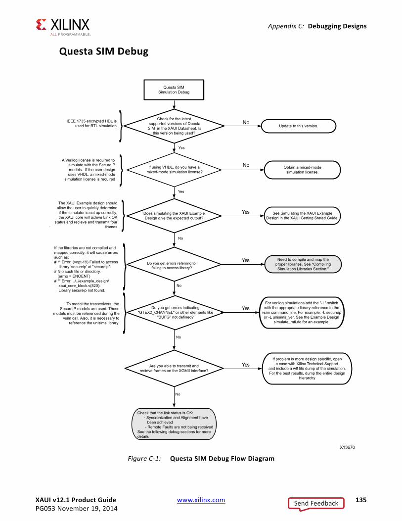
XAUI v12.1 Product Guide www.xilinx.com 135PG053 November 19, 2014
Appendix C: Debugging Designs
Questa SIM DebugX-Ref Target - Figure C-1
Figure C-1: Questa SIM Debug Flow Diagram
Send Feedback
XAUI v12.1 Product Guide www.xilinx.com 136PG053 November 19, 2014
Appendix C: Debugging Designs
Compiling Simulation LibrariesSimulation libraries must be compiled for third-party simulators when running outside of the Vivado IDE. Vivado Design Suite User Guide - Logic Simulation (UG900) [Ref 6].
Next StepIf the debug suggestions listed previously do not resolve the issue, open a support case to have the appropriate Xilinx expert assist with the issue.
To create a technical support case in WebCase, see the Xilinx website at:
www.xilinx.com/support/clearexpress/websupport.htm
Items to include when opening a case:
• Detailed description of the issue and results of the steps listed previously.
• Attach a VCD or WLF dump of the simulation.
To discuss possible solutions, use the Xilinx User Community: forums.xilinx.com/xlnx/
Hardware DebugHardware issues can range from link bring-up to problems seen after hours of testing. This section provides debug steps for common issues. The Vivado lab tools are a valuable resource to use in hardware debug and the signal names mentioned in the following individual sections can be probed using the Vivado lab tools for debugging the specif ic problems. Many of these common issue can also be applied to debugging design simulations.
General ChecksEnsure that all the timing constraints for the core were met during Place and Route.
• Does it work in timing simulation? If problems are seen in hardware but not in timing simulation, this could indicate a PCB issue.
• Ensure that all clock sources are clean. If using DCMs in the design, ensure that all DCMs have obtained lock by monitoring the locked port.
Monitoring the XAUI Core with Vivado Lab Tools• XGMII signals and signals between XAUI core and the transceiver can be added to
monitor data transmitted and received. See Table 2-6 and Table 2-7 for a list of signal names.
Send Feedback
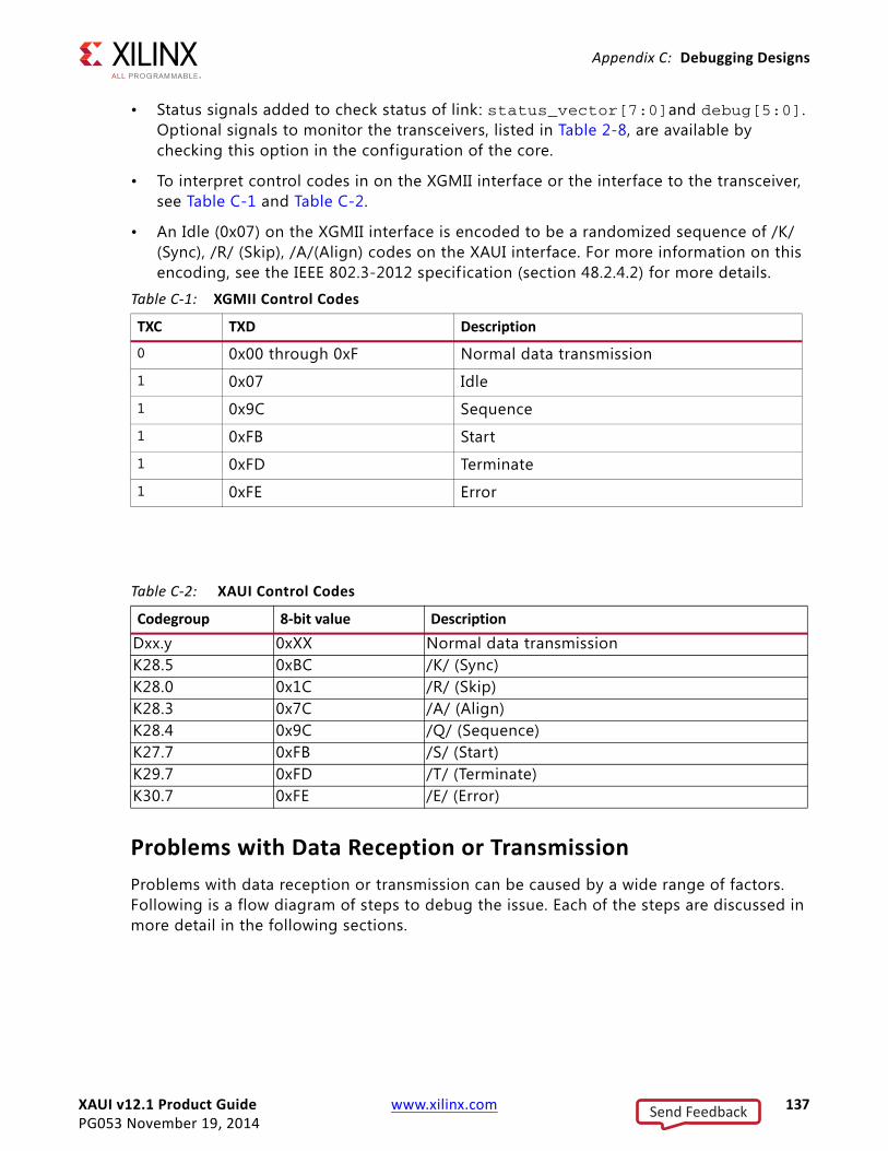
XAUI v12.1 Product Guide www.xilinx.com 137PG053 November 19, 2014
Appendix C: Debugging Designs
• Status signals added to check status of link: status_vector[7:0]and debug[5:0]. Optional signals to monitor the transceivers, listed in Table 2-8, are available by checking this option in the configuration of the core.
• To interpret control codes in on the XGMII interface or the interface to the transceiver, see Table C-1 and Table C-2.
• An Idle (0x07) on the XGMII interface is encoded to be a randomized sequence of /K/ (Sync), /R/ (Skip), /A/(Align) codes on the XAUI interface. For more information on this encoding, see the IEEE 802.3-2012 specif ication (section 48.2.4.2) for more details.
Problems with Data Reception or Transmission Problems with data reception or transmission can be caused by a wide range of factors. Following is a flow diagram of steps to debug the issue. Each of the steps are discussed in more detail in the following sections.
Table C-1: XGMII Control Codes
TXC TXD Description
0 0x00 through 0xF Normal data transmission
1 0x07 Idle
1 0x9C Sequence
1 0xFB Start
1 0xFD Terminate
1 0xFE Error
Table C-2: XAUI Control Codes
Codegroup 8-bit value DescriptionDxx.y 0xXX Normal data transmissionK28.5 0xBC /K/ (Sync)K28.0 0x1C /R/ (Skip)K28.3 0x7C /A/ (Align)K28.4 0x9C /Q/ (Sequence)K27.7 0xFB /S/ (Start)K29.7 0xFD /T/ (Terminate)K30.7 0xFE /E/ (Error)
Send Feedback
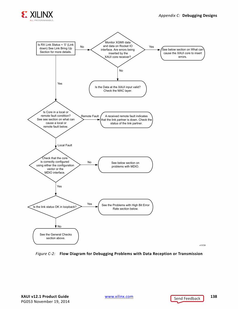
XAUI v12.1 Product Guide www.xilinx.com 138PG053 November 19, 2014
Appendix C: Debugging Designs
X-Ref Target - Figure C-2
Figure C-2: Flow Diagram for Debugging Problems with Data Reception or Transmission
Send Feedback
XAUI v12.1 Product Guide www.xilinx.com 139PG053 November 19, 2014
Appendix C: Debugging Designs
What Can Cause a Local or Remote Fault?Local Fault and Remote Fault codes both start with the sequence TXD/RXD=0x9C, TXC/RXC=1 in XGMII lane 0. Fault conditions can also be detected by looking at the status vector or MDIO registers. The Local Fault and Link Status are defined as latching error indicators by the IEEE specification. This means that the Local Fault and Link Status bits in the status vector or MDIO registers must be cleared with the Reset Local Fault bits and Link Status bits in the Configuration vector or MDIO registers.
Local Fault
The receiver outputs a local fault when the receiver is not up and operational. This RX local fault is also indicated in the status and MDIO registers. The most likely causes for an RX local fault are:
• The transceiver has not locked or the receiver is being reset.
• At least one of the lanes is not synchronized – debug[4:1]
• The lanes are not properly aligned – debug[5]
Note: The debug[5:0] signal is not latching.
A TX local fault is indicated in the status and MDIO registers when the transceiver transmitter is in reset or has not yet completed any other initialization or synchronization procedures needed.
Remote Fault
Remote faults are only generated in the MAC reconciliation layer in response to a Local Fault message. When the receiver receives a remote fault, this means that the link partner is in a local fault condition.
When the MAC reconciliation layer receives a remote fault, it silently drops any data being transmitted and instead transmits IDLEs to help the link partner resolve its local fault condition. When the MAC reconciliation layer receives a local fault, it silently drops any data being transmitted and instead transmits a remote fault to inform the link partner that it is in a fault condition. Be aware that the Xilinx 10GEMAC core has an option to disable remote fault transmission.
Send Feedback
XAUI v12.1 Product Guide www.xilinx.com 140PG053 November 19, 2014
Appendix C: Debugging Designs
Link Bring-UpThe following link initialization stages describe a possible scenario of the Link coming up between device A and device B.
Stage 1: Device A Powered Up, but Device B Powered Down
• Device A is powered up and reset.
• Device B powered down
• Device A detects a fault because there is no signal received. The Device A XAUI core indicates an RX local fault.
• The Device A MAC reconciliation layer receives the local fault. This triggers the MAC reconciliation layer to silently drop any data being transmitted and instead transmit a remote fault.
• RX Link Status = 0 (link down) in Device A X-Ref Target - Figure C-3
Stage 2: Device B Powers Up and Resets
• Device B powers up and resets.
• Device B XAUI completes Synchronization and Alignment.
• Device A has not synchronized and aligned yet. It continues to send remote faults.
• Device B XAUI passes received remote fault to MAC.
• Device B MAC reconciliation layer receives the remote fault. It silently drops any data being transmitted and instead transmits IDLEs.
• Link Status = '0' (link down) in both A and B.
Figure C-3: Device A Powered Up, but Device B Powered Down
Send Feedback
XAUI v12.1 Product Guide www.xilinx.com 141PG053 November 19, 2014
Appendix C: Debugging Designs
X-Ref Target - Figure C-4
Stage 3: Device A Receives Idle Sequence
• Device A XAUI RX detects idles, synchronizes and aligns.
• Device A reconciliation layer stops dropping frames at the output of the MAC transmitter and stops sending remote faults to Device B.
• Device A Link Status='1' (Link Up)
• When Device B stops receiving the remote faults, normal operation starts.X-Ref Target - Figure C-5
Stage 4: Normal Operation
In Stage 4 shown in Figure C-6, Device A and Device B have both powered up and been reset. The link status is 1 (link up) in both A and B and in both the MAC can transmit frames successfully.
X-Ref Target - Figure C-6
Figure C-4: Device B Powers Up and Resets
Figure C-5: Device A Receives Idle Sequence
Figure C-6: Normal Operation
Send Feedback
XAUI v12.1 Product Guide www.xilinx.com 142PG053 November 19, 2014
Appendix C: Debugging Designs
What Can Cause Synchronization and Alignment to Fail?Synchronization (debug[4:1]) occurs when each respective XAUI lane receiver is synchronized to byte boundaries. Alignment (debug[5]) occurs when the XAUI receiver is aligned across all four lanes.
Following are suggestions for debugging loss of Synchronization and Alignment:
• Monitor the state of the signal_detect[3:0] input to the core. This should either be:
• connected to an optical module to detect the presence of light. Logic 1 indicates that the optical module is correctly detecting light; logic 0 indicates a fault. Therefore, ensure that this is driven with the correct polarity.
• tied to logic 1 (if not connected to an optical module).
Note: When signal_detect is set to logic 0, this forces the receiver synchronization state machine of the core to remain in the loss of sync state.
• Loss of Synchronization can happen when invalid characters are received.
• Loss of Alignment can happen when invalid characters are seen or if an /A/ code is not seen in all four lanes at the same time.
• See the following section, Problems with a High Bit Error Rate.
Transceiver Specific
• Ensure that the polarities of the txn/txp and rxn/rxp lines are not reversed. If they are, these can be f ixed by using the txpolarity and rxpolarity ports of the transceiver, which can be accessed from outside the core by enabling the transceiver control and status port option.
• Check that the transceiver is not being held in reset or still be initialized by monitoring the mgt_tx_reset, mgt_rx_reset, and mgt_rxlock input signals to the XAUI encrypted HDL. The mgt_rx_reset signal is also asserted when there is an RX buffer error. An RX buffer error means that the Elastic Buffer in the receiver path of the transceiver is either under or overflowing. This indicates a clock correction issue caused by differences between the transmitting and receiving ends. Check all clock management circuitry and clock frequencies applied to the core and to the transceiver.
What Can Cause the XAUI Core to Insert Errors?On the receive path the XAUI core will insert errors RXD=FE, RXC=1, when disparity errors or invalid data are received or if the received interframe gap (IFG) is too small.
Send Feedback
XAUI v12.1 Product Guide www.xilinx.com 143PG053 November 19, 2014
Appendix C: Debugging Designs
Disparity Errors or Invalid Data
Disparity Errors or Invalid data can be checked for by monitoring the mgt_code_valid input to the XAUI core.
Small IFG
The XAUI Core inserts error codes into the Received XGMII data stream, RXD, when there are three or fewer IDLE characters (0x07) between frames. The error code (0xFE) precedes the frame "Terminate" delimiter (0xFD).
The IEEE 802.3-2012 specification (Section 46.2.1) requires a minimum interframe gap of f ive octets on the receive side. This includes the preceding frame Terminate control character and all Idles up to and immediately preceding the following frame Start control character. Because three (or fewer) Idles and one Terminate character are less than the required f ive octets, this would not meet the specif ication; therefore, the XAUI Core is expected to signal an error in this manner if the received frame does not meet the specif ication.
Problems with a High Bit Error Rate
Symptoms
If the link comes up but then goes down again or never comes up following a reset, the most likely cause for a RX Local Fault is a BER (Bit Error Rate) that is too high. A high BER causes incorrect data to be received, which leads to the lanes losing synchronization or alignment.
Debugging
Compare the issue across several devices or PCBs to ensure that the issue is not a one-off case.
• Try using an alternative link partner or test equipment and then compare results.
• Try putting the core into loopback (both by placing the core into internal loopback, and by looping back the optical cable) and compare the behavior. The core should always be capable of gaining synchronization and alignment when looping back with itself from transmitter to receiver so direct comparisons can be made. If the core exhibits correct operation when placed into internal loopback, but not when loopback is performed through an optical cable, this might indicate a faulty optical module or a PCB issue.
• Try swapping the optical module on a misperforming device and repeat the tests.
Send Feedback
XAUI v12.1 Product Guide www.xilinx.com 144PG053 November 19, 2014
Appendix C: Debugging Designs
Transceiver Specific Checks
• Monitor the mgt_codevalid[7:0] input to the XAUI core by triggering on it using the Vivado lab tools. This input is a combination of the transceiver RX disparity error and RX not in table error outputs.
• These signals should not be asserted over the duration of a few seconds, minutes or even hours. If they are frequently asserted, it might indicate an issue with the transceiver.
• Place the transceiver into parallel or serial near-end loopback.
• If correct operation is seen in the transceiver serial loopback, but not when loopback is performed through an optical cable, it might indicate a faulty optical module.
• If the core exhibits correct operation in the transceiver parallel loopback but not in serial loopback, this might indicate a transceiver issue.
• A mild form of bit error rate might be solved by adjusting the transmitter Pre-Emphasis and Differential Swing Control attributes of the transceiver.
Problems with the MDIOSee MDIO Interface for detailed information about performing MDIO transactions.
Things to check for:
• Ensure that the MDIO is driven properly. Check that the mdc clock is running and that the frequency is 2.5 MHz or less.
• Ensure that the XAUI core is not held in reset.
• Read from a configuration register that does not have all 0s as a default. If all 0s are read back, the read was unsuccessful. Check that the PRTAD field placed into the MDIO frame matches the value placed on the prtad[4:0] port of the XAUI core.
• Verify in simulation and/or a Vivado lab tools capture that the waveform is correct for accessing the host interface for a MDIO read/write.
Send Feedback
XAUI v12.1 Product Guide www.xilinx.com 145PG053 November 19, 2014
Appendix C: Debugging Designs
Next StepsIf the debug suggestions listed previously do not resolve the issue, open a support case to have the appropriate Xilinx expert assist with the issue.
To create a technical support case in Webcase, see the Xilinx website at:
www.xilinx.com/support/clearexpress/websupport.htm
Items to include when opening a case:
• Detailed description of the issue and results of the steps listed previously.
• Attach Vivado lab tools VCD captures taken in the steps previously.
To discuss possible solutions, use the Xilinx User Community:
forums.xilinx.com/xlnx/
Send Feedback
XAUI v12.1 Product Guide www.xilinx.com 146PG053 November 19, 2014
Appendix D
Additional Resources and Legal Notices
Xilinx ResourcesFor support resources such as Answers, Documentation, Downloads, and Forums, see Xilinx Support.
For a glossary of technical terms used in Xilinx® documentation, see the Xilinx Glossary.
References To search for Xilinx documentation, go to www.xilinx.com/support
1. 7 Series FPGAs GTX/GTH Transceiver User Guide (UG476)
2. 7 Series FPGAs GTP Transceiver User Guide (UG482)
3. UltraScale Architecture GTH Transceivers User Guide (UG576)
4. Vivado® Design Suite User Guide: Designing with IP (UG896)
5. Vivado Design Suite User Guide: Getting Started (UG910)
6. Vivado Design Suite User Guide - Logic Simulation (UG900)
7. UltraScale Architecture Migration Methodology Guide (UG1026)
8. ISE® to Vivado Design Suite Migration Guide (UG911)
9. Vivado Design Suite User Guide: Programming and Debugging (UG908)
10. Vivado Design Suite User Guide: Designing IP Subsystems using IP Integrator (UG994)
Send Feedback
XAUI v12.1 Product Guide www.xilinx.com 147PG053 November 19, 2014
Appendix D: Additional Resources and Legal Notices
Additional Core ResourcesFor detailed information about XAUI technology and updates to the XAUI core, see the following:
XAUI TechnologyFor information about XAUI technology basics, including features, FAQs, the XAUI device interface, typical applications, specif ications, and other important information, see www.xilinx.com/products/ipcenter/XAUI.htm.
Ethernet SpecificationsRelevant XAUI IEEE standards, which can be downloaded in PDF format from standards.ieee.org/getieee802/: IEEE Std. 802.3-2012
Other InformationThe 10-Gigabit Ethernet Consortium at the University of New Hampshire Interoperability Lab is an excellent source of information on 10-Gigabit Ethernet technology: www.iol.unh.edu/consortiums/10gec/index.html.
Revision HistoryThe following table shows the revision history for this document.
Date Version Revision
11/19/2014 12.1 • Updated IEEE Std. 802.3-2012.• Updated Register Bit Definitions• Updated figures in Interfacing to the Core and Design Considerations
chapters.
06/04/2014 12.1 • Added User Parameters to Design Flow Steps chapter.• Added Device Migration to Migrating and Upgrading appendix.
04/02/2014 12.1 • Replaced “Kintex UltraScale” with UltraScale “architecture”.• Added example xdc for placement of GTHE3 transceivers in UltraScale
architecture.
Send Feedback
XAUI v12.1 Product Guide www.xilinx.com 148PG053 November 19, 2014
Appendix D: Additional Resources and Legal Notices
Please Read: Important Legal NoticesThe information disclosed to you hereunder (the "Materials") is provided solely for the selection and use of Xilinx products. To the maximum extent permitted by applicable law: (1) Materials are made available "AS IS" and with all faults, Xilinx hereby DISCLAIMS ALL WARRANTIES AND CONDITIONS, EXPRESS, IMPLIED, OR STATUTORY, INCLUDING BUT NOT LIMITED TO WARRANTIES OF MERCHANTABILITY, NON-INFRINGEMENT, OR FITNESS FOR ANY PARTICULAR PURPOSE; and (2) Xilinx shall not be liable (whether in contract or tort, including negligence, or under any other theory of liability) for any loss or damage of any kind or nature related to, arising under, or in connection with, the Materials (including your use of the Materials), including for any direct, indirect, special, incidental, or consequential loss or damage (including loss of data, profits, goodwill, or any type of loss or damage suffered as a result of any action brought by a third party) even if such damage or loss was reasonably foreseeable or Xilinx had been advised of the possibility of the same. Xilinx assumes no obligation to correct any errors contained in the Materials or to notify you of updates to the Materials or to product specifications. You may not reproduce, modify, distribute, or publicly display the Materials without prior written consent. Certain products are subject to the terms and conditions of Xilinx's limited warranty, please refer to Xilinx's Terms of Sale which can be viewed at http://www.xilinx.com/legal.htm#tos; IP cores may be subject to warranty and support terms contained in a license issued to you by Xilinx. Xilinx products are not designed or intended to be fail-safe or for use in any application requiring fail-safe performance; you assume sole risk and liability for use of Xilinx products in such critical applications, please refer to Xilinx's Terms of Sale which can be viewed at http://www.xilinx.com/legal.htm#tos.© Copyright 2012–2014 Xilinx, Inc. Xilinx, the Xilinx logo, Artix, ISE, Kintex, Spartan, Virtex, Vivado, Zynq, and other designated brands included herein are trademarks of Xilinx in the United States and other countries. The PowerPC name and logo are registered trademarks of IBM Corp. and used under license. All other trademarks are the property of their respective owners.
12/18/2013 12.1 • Added UltraScale™ architecture support.• Updated resource tables for all devices.• Updated Transceiver Control and Status Ports table for 7 Series FPGAs.• Added Transceiver Control and Status Ports table for Kintex® UltraScale™
devices.• Added clocking example deign information for Kintex UltraScale devices.
10/02/2013 12.0 • Revision number advanced to 12.0 to align with core version number.• Updated clocking scheme.• Added transceiver control and status port support. Updated Table 2-7.• Added “Upgrading in the Vivado Design Suite” section to Appendix B,
Migrating and Upgrading• Updated screen captures in Chapter 7.
03/20/2013 2.0 • Updated for core version 11.0 and Vivado Design Suite release.• Removed all ISE, Virtex®-6, Virtex-5, Virtex-4, and Spartan®-6 material.• Updated Debug appendix.• Added core top level changes to include transceivers and supporting logic.• Added hierarchical XDC support.• Added Artix®-7 FPGA 20G support.
07/25/2012 1.0 Initial Xilinx release. This new product guide is based on ds266 and ug150.
Date Version Revision
Send Feedback