Embed Size (px)
Citation preview

X-ray Nano Probes for Nano Materials
at Taiwan Photon Source
TPS
TLS

2
Outline
• Synchrotron Light Source
• Application of Synchrotron Light
• X-ray nano probe at TPS

“Light” is indispensable to man‘s exploration of nature

http://www.yingfukeji.com/appl/grid.html
http://www.uv-teck.com/Ttwjy
http://www.hko.gov.hk/prtver/html/docs/education/ed
u02rga/radiation/radiation_02-c.shtml
http://smallcollation.blogspot.tw/2014/02/infra
red-spectroscopy-of-alkanes.html#gsc.tab=0
Invisible light: IR and X-ray…

Rontgen used a simple accelerator to discover X-rays


二極偏轉磁鐵

1
3
4
6
5
8
9
10
7
2
同步加速器光源的原理電子在電子槍(1)內產生,經過直線加速器(2)加速至能量為5,000萬電子伏特。
電子束進入增能環(3)後,繼續增加能量至15億電子伏特(1.5GeV),速度非常接近光速(0.99999995倍)。
電子束經由傳輸線(4)進入儲存環(5) 。
當儲存環累積足夠的電子束後,經由各個磁鐵的導引與聚焦,電子束在偏轉磁鐵(6)及插件磁鐵(7)發出同步加速器光源,經由光束線(8)將光源引導至實驗站(9)進行實驗。
電子束在發出同步加速器光源後,要靠高頻腔(10)來補充失去的能量。

1. 電子槍 2. 直線加速器
3. 增能環4. 傳輸線5. 儲存環
8. 光束線
6. 偏轉磁鐵
7. 插件磁鐵
9. 實驗站 10. 高頻系統
加速器與實驗設施

儲存環 3D 圖
偏轉磁鐵高頻系統
偏轉磁鐵超導高頻腔
超導增頻磁鐵 聚頻磁鐵


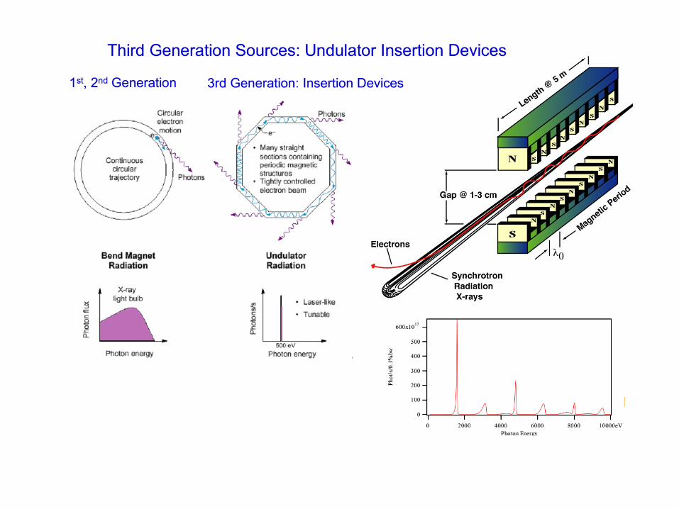


Unique Features of Synchrotron
Light Source• High intensity
• Continuous spectrum
• Excellent collimation
• High polarization
• Pulsed-time structure
以X光為例,同步加速器光源在這個波段的亮度比傳統X光機還要強百萬倍以上!過去需要幾個月才能完成的實驗,現在只需幾分鐘便能得到結果。以往因實驗光源亮度不夠而無法探測的結構,現在藉由同步加速器光源,都可分析得一清二楚,也因此得以開發新的研究領域。


Beamline


25
Outline
• Synchrotron Light Source
• Application of Synchrotron Light
• X-ray nano probe at TPS


TLSTPS
NSRRC is constructing a low-emittance synchrotron-
based light source, Taiwan Photon Source (TPS)
3 Gev
518.4 m
500 mA
1.6nm-rad


47
Outline
• Synchrotron Light Source
• Application of Synchrotron Light
• X-ray nano probe at TPS

Beamline specification
Energy range:4 - 15 keV
Photon flux:1010 ~1011 photons/sec
Energy resolution:< 2×10⁻⁴ with Si(111) crystals
Beam size:~ 40 nm at 10 keV (H × V,
FWHM)
High-order harmonic contamination:≦1 × 10⁻⁴
Energy scanning capabilities.
X-ray Methods:With tens-nm resolution (incoherent)
• nano-XRF (x-ray fluorescence)
• Element-specific nanoimaging
• nano-XAFS (x-ray absorption fine structures)
• Local electronic structure
• Local chemical environments
• Element-specific, averaged over nano-size area
• nano-XEOL (x-ray excited optical luminescence)
• X-ray-to-visible down-conversion efficiency in
nano phosphor
• nano-PXM (projection x-ray microscopy)
•Absorption and phase contrast x-ray images
Beyond sub-ten-nm resolution (coherent)
• nano-CXDI (coherent x-ray diffraction imaging)
• Bragg-ptychograpgy
• strain dynamics in nano-devices
48
Other than X-rays
• SEM (SE, EDS, CL with high spatial resolution)• Fly scanning • Nanomotors (optional)• Sample environment -heat, electric, L-He (optional)

49
TPS 23A XNP
Endstation Schedule
1. Montel mirror2. Sample Stage3. Laser interferometer4. XEOL5. SEM6. EDS 7. Sample Preparation system8. Portable sample transfer9. Projection CCD10. Diffraction detector
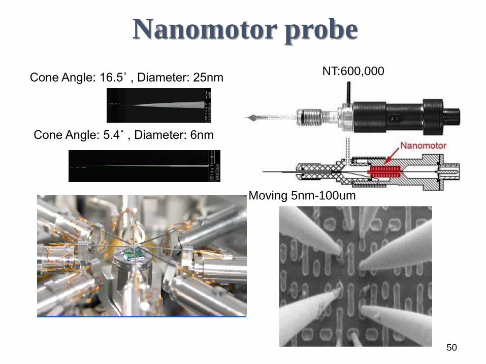
Nanomotor probe
Moving 5nm-100um
50
Cone Angle: 16.5˚ , Diameter: 25nm
Cone Angle: 5.4˚ , Diameter: 6nm
NT:600,000

Nanometer can construct
the 4-point probe
Substrate
Force Force
I-V measurement I-V measurement
I-V measurement I-V measurement
P-MOS
P-MOS
N-MOS
N-MOS
X-ray
X-ray
51
Nanomotor Probe Application
Force Force

52

• Montel nested KB mirror @ TPS:
Montel Nested KB Mirror @TPS-23A
Profile of KB mirror
Minimum radius : 20 m
• Montel nested KB mirror @ APS:
• Focal spot: 100 nm
• Challenges:
• Gap between mirrors
• Slope error
Overcome by Elastic Emission Machining
(EEM)
Objective distance 69 m
Focus length 11 cm
Mirror length 11 cm
Slope error (RMS) < 0.05 μrad
Incident angle 4 mrad
Coating Rh
Material silica
Working Distance 5.5 cm

Montel KB Montel Mirror and Holders
A1 X
A2 Y
A3 Z
A4 Pitch
A5 Roll
A6 Yaw
A7 Top-Y
A8 Top-Z
A9 Top-pitch(X)
A1
0Top-Roll (Y)
M1 Top-X (Manual)
M2 Top-yaw (Manual)
A2
A1
A3
A4 A5
A6
A7,A8
M1
A9
A10
June 2015, at JTEC
Montel Mirror on the holder
Gap imaged by
microscope
M2

40nm
5.656 mrad
4.0 mrad
Simulation of Focus SpotSimulation at 10 keV, average reflection=0.802, by ray tracing
Source size 12.5 μm x 12.5 μm
Source divergence 6μrad x 6μrad
FHWM 32nm x 32nm,
Simulated
Focus spot size
Simulated
DivergenceBy Gung-Chian Yin

• Montel nested KB mirror @ TPS:
Montel Nested KB Mirror @TPS-23A
Profile of KB mirror
Minimum radius : 20 m
• Montel nested KB mirror @ APS:
• Focal spot: 100 nm
• Challenges:
• Gap between mirrors
• Slope error
Overcome by Elastic Emission Machining
(EEM)
Objective distance 69 m
Focus length 11 cm
Mirror length 11 cm
Slope error (RMS) < 0.05 μrad
Incident angle 4 mrad
Coating Rh
Material silica
Working Distance 5.5 cm

Montel KB Montel Mirror and Holders
A1 X
A2 Y
A3 Z
A4 Pitch
A5 Roll
A6 Yaw
A7 Top-Y
A8 Top-Z
A9 Top-pitch(X)
A1
0Top-Roll (Y)
M1 Top-X (Manual)
M2 Top-yaw (Manual)
A2
A1
A3
A4 A5
A6
A7,A8
M1
A9
A10
June 2015, at JTEC
Montel Mirror on the holder
Gap imaged by
microscope
M2


59
Doping method:Ion implantation and thermal annealingElemental map of XRF
SEM
Doping of ZnO NWs by transition metal Co.Application : Spintronic deviceWant to know:• Distribution• Short structure order• Elemental composition
Pink beam mode at 12 KeV Pixel size : 25 x 25 nm2
Accumulation time : 0.5 sec/point beam size : 60 x 60 nm2 (V x H)
Vapour-liguid-solid processNano Lett. 2011, 11, 5322–5326
nano-XRF (x-ray fluorescence)
Element-specific nano-imaging
500nm

60

61
nano-XAFS (x-ray absorption fine structures)– Local electronic structure
– Local chemical environments
– Element-specific, averaged over nano-area

62
• 200 nm thick SiN membranes. • Without XRF background signal• X-ray diffraction can be
transmitted
ESRF ID16B methods
XEOL•Multimode optical fiber• UV-VIS : linear CCD Si detector•Si avalanche photodiode (id100 from id-Quantique) XRD
•The XRD signal was measured using a fast readout low noise (FReLoN) CCD detector.• The CCD images were processed using Fit2D software to generate the standard diffractograms.• Using the experimental parameters derived from the measurement of an Al2O3 reference sample.
XRF• XRF signal was collected at 15°• The elemental composition of the NWs was estimated
by fitting the XRF spectra using the PyMca program.• XANES spectra were recorded in X-ray fluorescence
mode with a step size of 1 eV and integration times determined by the counting statistics.
• The data analysis was performed using the IFEFFIT package.

63
nano-XEOL (x-ray excited optical luminescence) &
CL (cathodoluminescsnce)
XEOL: 1.nano-area
2.multi-layer, buried layer
Doping species, Band gap, Defect band,
Charge transport

64
nano-PXM (projection x-ray microscopy) –Absorption and phase contrast x-ray images

X-ray Bragg projection ptychography from
thin film heterostructures
15nm
65nm
11.2kev
85nm
Ki
Kf
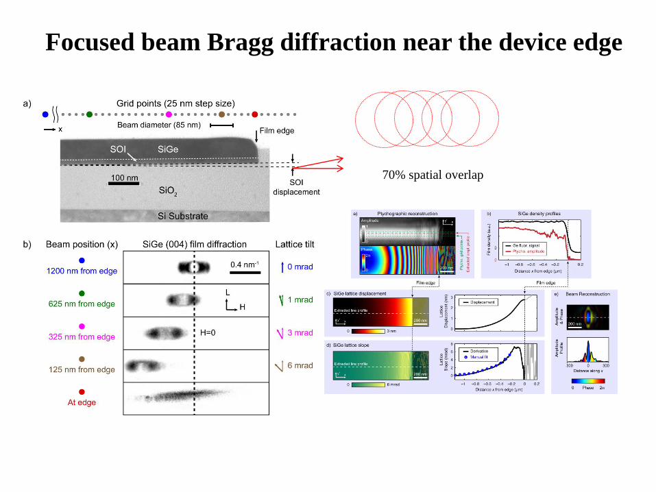
Focused beam Bragg diffraction near the device edge
70% spatial overlap

67
Upgrade: Hard X-ray photoelectron
spectroscope(HXPS) at XNP
K. Kobayashi, Nuclear Instruments and Methods in Physics
Research A 601 (2009) 32–47
HXPS: Several keV to 15 keV to
increase bulk sensitivity for bulk
electronic structure and buried
interface.

6868
Solid state physics• Strongly correlated electron systems
YbAl3, YbInCu4, YbCu2Si2
La1-xSrxMnO3 (LSMO)
• Spintronics
LaVO3, LaAlO3, Fe3-xMxO4(M=Mn, Zn)
• Compound semiconductors
InGaZnO, GaCrN, InN, ZnMgO
High-k gate stacks
M. Chu, et al., Annu. Rev. Mater. Res.
39 (2009) 203-229
Applications