Embed Size (px)
Citation preview
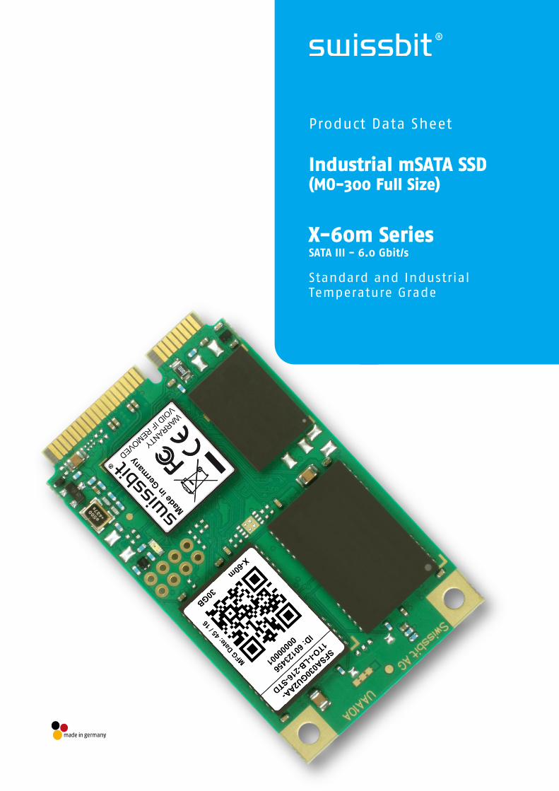
Product Data Sheet
Industrial mSATA SSD (MO-300 Full Size)
X-60m Series SATA III - 6.0 Gbit/s
Standard and Industrial
Temperature Grade
Swissbit AG Revision: 1.06 Industriestrasse 4-8
CH-9552 Bronschhofen www.swissbit.com X-60m_data_sheet_SA-UxAA_Rev106.docx Switzerland [email protected] Page 2 of 22
Contents 1. PRODUCT SUMMARY ............................................................................................................ 3
2. PRODUCT FEATURES ............................................................................................................ 4
3. ORDERING INFORMATION ...................................................................................................... 5
4. PRODUCT DESCRIPTION ......................................................................................................... 6
4.1 PERFORMANCE SPECIFICATIONS ...................................................................................................... 7 4.2 CURRENT CONSUMPTION ............................................................................................................ 7 4.3 ENVIRONMENTAL SPECIFICATIONS .................................................................................................. 8 4.4 REGULATORY COMPLIANCE ..........................................................................................................9 4.5 MECHANICAL SPECIFICATIONS .......................................................................................................9 4.6 RELIABILITY AND ENDURANCE .....................................................................................................10 4.7 DRIVE GEOMETRY SPECIFICATION ...................................................................................................10
5. ELECTRICAL INTERFACE ......................................................................................................... 11
6. PACKAGE MECHANICAL ........................................................................................................ 12
7. ATA COMMANDS ............................................................................................................... 13
8. IDENTIFY DEVICE INFORMATION .............................................................................................. 15
9. S.M.A.R.T. FUNCTIONALITY ................................................................................................... 16
9.1 S.M.A.R.T. SUBCOMMANDS ...................................................................................................... 16 9.2 S.M.A.R.T. READ DATA .......................................................................................................... 17 9.3 S.M.A.R.T. ATTRIBUTES ......................................................................................................... 17 9.4 S.M.A.R.T. ATTRIBUTE ENTRY STRUCTURE ........................................................................................18
10. PART NUMBER DECODER ...................................................................................................... 19
10.1 MANUFACTURER .................................................................................................................. 19 10.2 MEMORY TYPE ................................................................................................................... 19 10.3 PRODUCT TYPE ................................................................................................................... 19 10.4 DENSITY ......................................................................................................................... 19 10.5 PLATFORM ....................................................................................................................... 19 10.6 PRODUCT GENERATION ........................................................................................................... 19 10.7 MEMORY ORGANIZATION ......................................................................................................... 19 10.8 TECHNOLOGY ..................................................................................................................... 19 10.9 NUMBER OF FLASH CHIPS ........................................................................................................ 19 10.10 FLASH CODE ................................................................................................................... 20 10.11 TEMPERATURE OPTION .......................................................................................................... 20 10.12 DIE CLASSIFICATION............................................................................................................. 20 10.13 PIN MODE ..................................................................................................................... 20 10.14 DRIVE CONFIGURATION XYZ .................................................................................................... 20 10.15 OPTION ........................................................................................................................ 20
11. SWISSBIT MSATA SSD MARKING SPECIFICATION ............................................................................ 21
11.1 TOP VIEW ......................................................................................................................... 21 11.2 LABEL CONTENT ................................................................................................................... 21
12. REVISION HISTORY ............................................................................................................. 22
Swissbit AG Revision: 1.06 Industriestrasse 4-8
CH-9552 Bronschhofen www.swissbit.com X-60m_data_sheet_SA-UxAA_Rev106.docx Switzerland [email protected] Page 3 of 22
X-60m Series – Industrial mSATA Solid State Drive 8 GBytes Up to 480 GBytes (MO-300A)
1. Product Summary Capacities: 8 GBytes, 16 GBytes, 30 GBytes, 60 GBytes, 120 GBytes, 240 GBytes, 480 GBytes
Form Factor:
o JEDEC MO-300A Sized Solid State Drive (50.8 mm x 29.85 mm x 3.5 mm)
o 52-Pin PCI Express (PCIe) Mini-Connector (SATA III)
Compliance: SATA Rev 3.1 - 6 Gbit/s (3 Gbit/s and 1.5 Gbit/s backward compatible)
Command Sets: Supports ATA/ATAPI-8 and ACS-2 (2011/06/22)
Performance:
o Burst Transfer Rate: Up to 600 MBytes/s in SATA III - 6.0 Gbit/s
o Read Performance: Sequential Read up to 520 MBytes/s, Random Read IOPs up to 75,000
o Write Performance: Sequential Write up to 450 MBytes/s, Random Write IOPs up to 75,000
Operating Temperature Range1:
o Commercial: 0 °C to 70 °C
o Industrial: -40 °C to 85 °C
Storage Temperature Range: -40 °C to 85 °C
Operating Voltage: 3.3 V ± 5%
Power (Max Capacity):
o Read (Active): 1.5 W
o Write (Active): 3.2 W
o Idle: 380 mW
o Slumber: 115 mW
Data Retention: 10 Years @ Life Begin; 1 Year @ Life End
Endurance: TeraBytes Written (TBW) @ Max Capacity2
o Client > 975
o Embedded > 280
o Enterprise > 235
Shock/Vibration: 1,500 g/20 g (MIL-STD810)
High-Performance 32-Bit Processor with Integrated, Parallel Flash Interface Engines:
o Multi-Level Cell (MLC) NAND Flash
o Hardware BCH Code ECC (up to 66 bit correction per 1 KByte page)
High Reliability:
o Mean Time Between Failure (MTBF): > 2,000,000 hours
o Data Reliability: < 1 non-recoverable error per 1016 bits read
1 Adequate airflow is required to ensure the drive temperature, as reported in the S.M.A.R.T. data, does not exceed the specified
maximum operating temperature. 2 According to JEDEC (JESD47I), the time to write the full TBW is 18 months. Higher average daily data volume reduces the specified TBW.
Swissbit AG Revision: 1.06 Industriestrasse 4-8
CH-9552 Bronschhofen www.swissbit.com X-60m_data_sheet_SA-UxAA_Rev106.docx Switzerland [email protected] Page 4 of 22
2. Product Features Best-in-Class Performance and Endurance with durabit™ Technology
Dynamic and Static Wear Leveling
Page Mode Flash Translation Layer (FTL)
Data Care Management
o Active: Adaptive Read Refresh
o Passive: Background Media Scan
Lifetime Enhancements
o Dynamic Bad Block Remapping
o Write Amplification Reduction
On-Board Power Fail Protection
AHCI, TRIM, and NCQ Support
ATA Security Feature Set Support
DEVSLP Compatible
In-Field Firmware Update
Enterprise-Grade Self-Monitoring, Analysis, and Reporting Technology (S.M.A.R.T.)
30 µinch Gold-Plated Connector (IPC-6012B Class 2 Compliant)
Life Cycle Management
Controlled “Locked” BOM
RoHS-6 Compliant
AES256 Encryption (on request)
Swissbit Life Time Monitoring (SBLTM) Tool and SDK for SBLTM (on request)
Swissbit AG Revision: 1.06 Industriestrasse 4-8
CH-9552 Bronschhofen www.swissbit.com X-60m_data_sheet_SA-UxAA_Rev106.docx Switzerland [email protected] Page 5 of 22
3. Ordering Information
Table 1: Standard Product List
Capacity Part Number
8 GBytes SFSA008GUxAA1TO-t-GS-2y6-STD
16 GBytes SFSA016GUxAA2TO-t-GS-2y6-STD
30 GBytes SFSA030GUxAA1TO-t-LB-2y6-STD
60 GBytes SFSA060GUxAA2TO-t-LB-2y6-STD
120 GBytes SFSA120GUxAA4TO-t-LB-2y6-STD
240 GBytes SFSA240GUxAA4TO-t-HC-2y6-STD
480 GBytes SFSA480GUxAA4TO-t-OC-2y6-STD
x = product generation; t = temperature; y= firmware revision
Table 2: Part Numbers Available for Ordering
Capacity Commercial Temperature Industrial Temperature
Part Number Part Number
8 GBytes SFSA008GU2AA1TO-C-GS-216-STD SFSA008GU2AA1TO-I-GS-216-STD
16 GBytes SFSA016GU2AA2TO-C-GS-216-STD SFSA016GU2AA2TO-I-GS-216-STD
30 GBytes SFSA030GU2AA1TO-C-LB-216-STD SFSA030GU2AA1TO-I-LB-216-STD
60 GBytes SFSA060GU2AA2TO-C-LB-216-STD SFSA060GU2AA2TO-I-LB-216-STD
120 GBytes SFSA120GU2AA4TO-C-LB-216-STD SFSA120GU2AA4TO-I-LB-216-STD
240 GBytes SFSA240GU2AA4TO-C-HC-216-STD SFSA240GU2AA4TO-I-HC-216-STD
480 GBytes SFSA480GU2AA4TO-C-OC-216-STD SFSA480GU2AA4TO-I-OC-216-STD
Swissbit AG Revision: 1.06 Industriestrasse 4-8
CH-9552 Bronschhofen www.swissbit.com X-60m_data_sheet_SA-UxAA_Rev106.docx Switzerland [email protected] Page 6 of 22
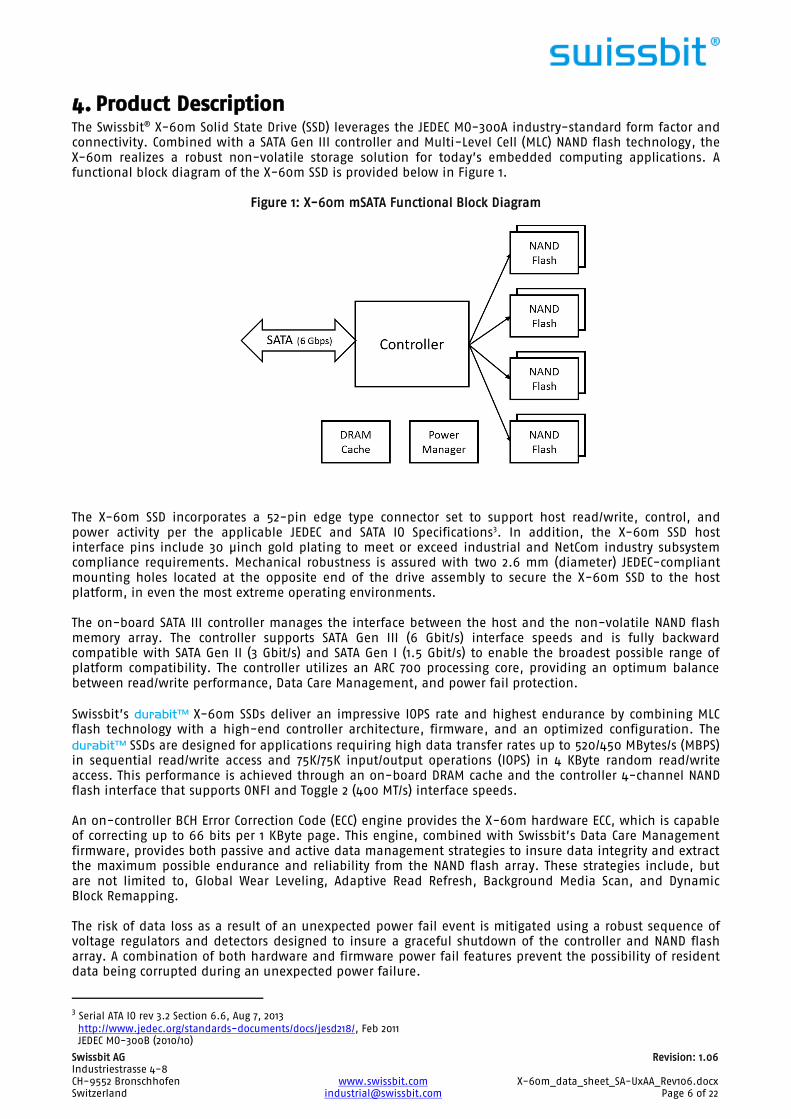
4. Product Description The Swissbit® X-60m Solid State Drive (SSD) leverages the JEDEC MO-300A industry-standard form factor and
connectivity. Combined with a SATA Gen III controller and Multi-Level Cell (MLC) NAND flash technology, the
X-60m realizes a robust non-volatile storage solution for today’s embedded computing applications. A
functional block diagram of the X-60m SSD is provided below in Figure 1.
Figure 1: X-60m mSATA Functional Block Diagram
The X-60m SSD incorporates a 52-pin edge type connector set to support host read/write, control, and
power activity per the applicable JEDEC and SATA IO Specifications3. In addition, the X-60m SSD host
interface pins include 30 µinch gold plating to meet or exceed industrial and NetCom industry subsystem
compliance requirements. Mechanical robustness is assured with two 2.6 mm (diameter) JEDEC-compliant
mounting holes located at the opposite end of the drive assembly to secure the X-60m SSD to the host
platform, in even the most extreme operating environments.
The on-board SATA III controller manages the interface between the host and the non-volatile NAND flash
memory array. The controller supports SATA Gen III (6 Gbit/s) interface speeds and is fully backward
compatible with SATA Gen II (3 Gbit/s) and SATA Gen I (1.5 Gbit/s) to enable the broadest possible range of
platform compatibility. The controller utilizes an ARC 700 processing core, providing an optimum balance
between read/write performance, Data Care Management, and power fail protection.
Swissbit’s durabit™ X-60m SSDs deliver an impressive IOPS rate and highest endurance by combining MLC
flash technology with a high-end controller architecture, firmware, and an optimized configuration. The
durabit™ SSDs are designed for applications requiring high data transfer rates up to 520/450 MBytes/s (MBPS)
in sequential read/write access and 75K/75K input/output operations (IOPS) in 4 KByte random read/write
access. This performance is achieved through an on-board DRAM cache and the controller 4-channel NAND
flash interface that supports ONFI and Toggle 2 (400 MT/s) interface speeds.
An on-controller BCH Error Correction Code (ECC) engine provides the X-60m hardware ECC, which is capable
of correcting up to 66 bits per 1 KByte page. This engine, combined with Swissbit’s Data Care Management
firmware, provides both passive and active data management strategies to insure data integrity and extract
the maximum possible endurance and reliability from the NAND flash array. These strategies include, but
are not limited to, Global Wear Leveling, Adaptive Read Refresh, Background Media Scan, and Dynamic
Block Remapping.
The risk of data loss as a result of an unexpected power fail event is mitigated using a robust sequence of
voltage regulators and detectors designed to insure a graceful shutdown of the controller and NAND flash
array. A combination of both hardware and firmware power fail features prevent the possibility of resident
data being corrupted during an unexpected power failure.
3 Serial ATA IO rev 3.2 Section 6.6, Aug 7, 2013
http://www.jedec.org/standards-documents/docs/jesd218/, Feb 2011 JEDEC MO-300B (2010/10)
Swissbit AG Revision: 1.06 Industriestrasse 4-8
CH-9552 Bronschhofen www.swissbit.com X-60m_data_sheet_SA-UxAA_Rev106.docx Switzerland [email protected] Page 7 of 22
Related Documentation Serial Transport Protocols and Physical Interconnect (ATA/ATAPI-8)
AT Attachment Interface Document, American National Standards Institute, X3.298-1997
JEDEC MO-300 standard - JEDEC Publication 95: Registered and Standard Outlines for Solid State and
Related Products
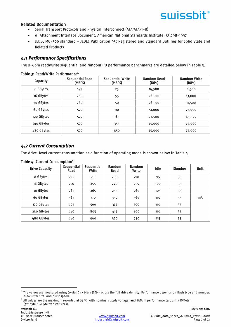
4.1 Performance Specifications
The X-60m read/write sequential and random I/O performance benchmarks are detailed below in Table 3.
Table 3: Read/Write Performance4
Capacity Sequential Read
(MBPS)
Sequential Write
(MBPS)
Random Read
(IOPs)
Random Write
(IOPs)
8 GBytes 145 25 14,500 6,500
16 GBytes 280 55 26,500 13,000
30 GBytes 280 50 26,500 11,500
60 GBytes 520 90 51,000 23,000
120 GBytes 520 185 73,500 45,500
240 GBytes 520 355 75,000 75,000
480 GBytes 520 450 75,000 75,000
4.2 Current Consumption
The drive-level current consumption as a function of operating mode is shown below in Table 4.
Table 4: Current Consumption5
Drive Capacity Sequential
Read
Sequential
Write
Random
Read
Random
Write Idle Slumber Unit
8 GBytes 205 210 200 210 95 35
mA
16 GBytes 250 255 240 255 100 35
30 GBytes 265 265 255 265 105 35
60 GBytes 365 370 330 365 110 35
120 GBytes 405 500 375 500 110 35
240 GBytes 440 805 415 800 110 35
480 GBytes 440 960 420 950 115 35
4 The values are measured using Crystal Disk Mark (CDM) across the full drive density. Performance depends on flash type and number,
file/cluster size, and burst speed. 5 All values are the maximum recorded at 25 °C, with nominal supply voltage, and SATA III performance test using IOMeter
(512 byte-1 MByte transfer sizes).
Swissbit AG Revision: 1.06 Industriestrasse 4-8
CH-9552 Bronschhofen www.swissbit.com X-60m_data_sheet_SA-UxAA_Rev106.docx Switzerland [email protected] Page 8 of 22
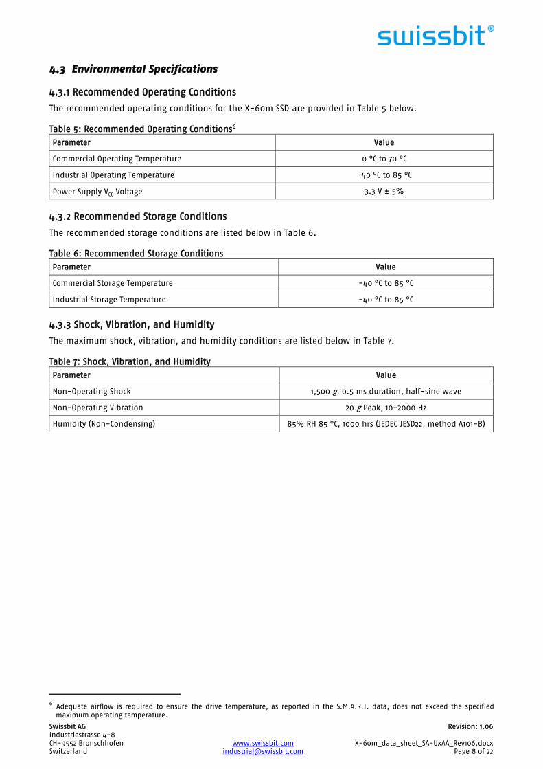
4.3 Environmental Specifications
4.3.1 Recommended Operating Conditions
The recommended operating conditions for the X-60m SSD are provided in Table 5 below.
Table 5: Recommended Operating Conditions6
Parameter Value
Commercial Operating Temperature 0 °C to 70 °C
Industrial Operating Temperature -40 °C to 85 °C
Power Supply VCC Voltage 3.3 V ± 5%
4.3.2 Recommended Storage Conditions
The recommended storage conditions are listed below in Table 6.
Table 6: Recommended Storage Conditions
Parameter Value
Commercial Storage Temperature -40 °C to 85 °C
Industrial Storage Temperature -40 °C to 85 °C
4.3.3 Shock, Vibration, and Humidity
The maximum shock, vibration, and humidity conditions are listed below in Table 7.
Table 7: Shock, Vibration, and Humidity
Parameter Value
Non-Operating Shock 1,500 g, 0.5 ms duration, half-sine wave
Non-Operating Vibration 20 g Peak, 10-2000 Hz
Humidity (Non-Condensing) 85% RH 85 °C, 1000 hrs (JEDEC JESD22, method A101-B)
6 Adequate airflow is required to ensure the drive temperature, as reported in the S.M.A.R.T. data, does not exceed the specified
maximum operating temperature.
Swissbit AG Revision: 1.06 Industriestrasse 4-8
CH-9552 Bronschhofen www.swissbit.com X-60m_data_sheet_SA-UxAA_Rev106.docx Switzerland [email protected] Page 9 of 22
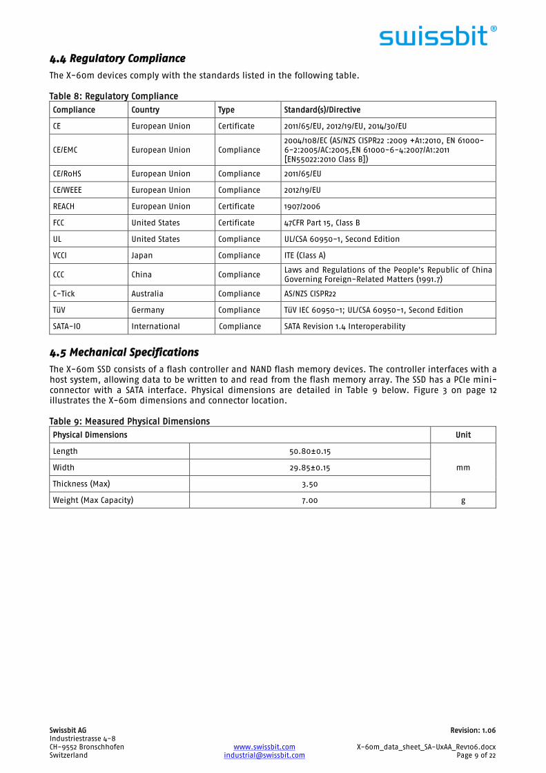
4.4 Regulatory Compliance
The X-60m devices comply with the standards listed in the following table.
Table 8: Regulatory Compliance
Compliance Country Type Standard(s)/Directive
CE European Union Certificate 2011/65/EU, 2012/19/EU, 2014/30/EU
CE/EMC European Union Compliance
2004/108/EC (AS/NZS CISPR22 :2009 +A1:2010, EN 61000-
6-2:2005/AC:2005,EN 61000-6-4:2007/A1:2011
[EN55022:2010 Class B])
CE/RoHS European Union Compliance 2011/65/EU
CE/WEEE European Union Compliance 2012/19/EU
REACH European Union Certificate 1907/2006
FCC United States Certificate 47CFR Part 15, Class B
UL United States Compliance UL/CSA 60950-1, Second Edition
VCCI Japan Compliance ITE (Class A)
CCC China Compliance Laws and Regulations of the People's Republic of China
Governing Foreign-Related Matters (1991.7)
C-Tick Australia Compliance AS/NZS CISPR22
TüV Germany Compliance TüV IEC 60950-1; UL/CSA 60950-1, Second Edition
SATA-IO International Compliance SATA Revision 1.4 Interoperability
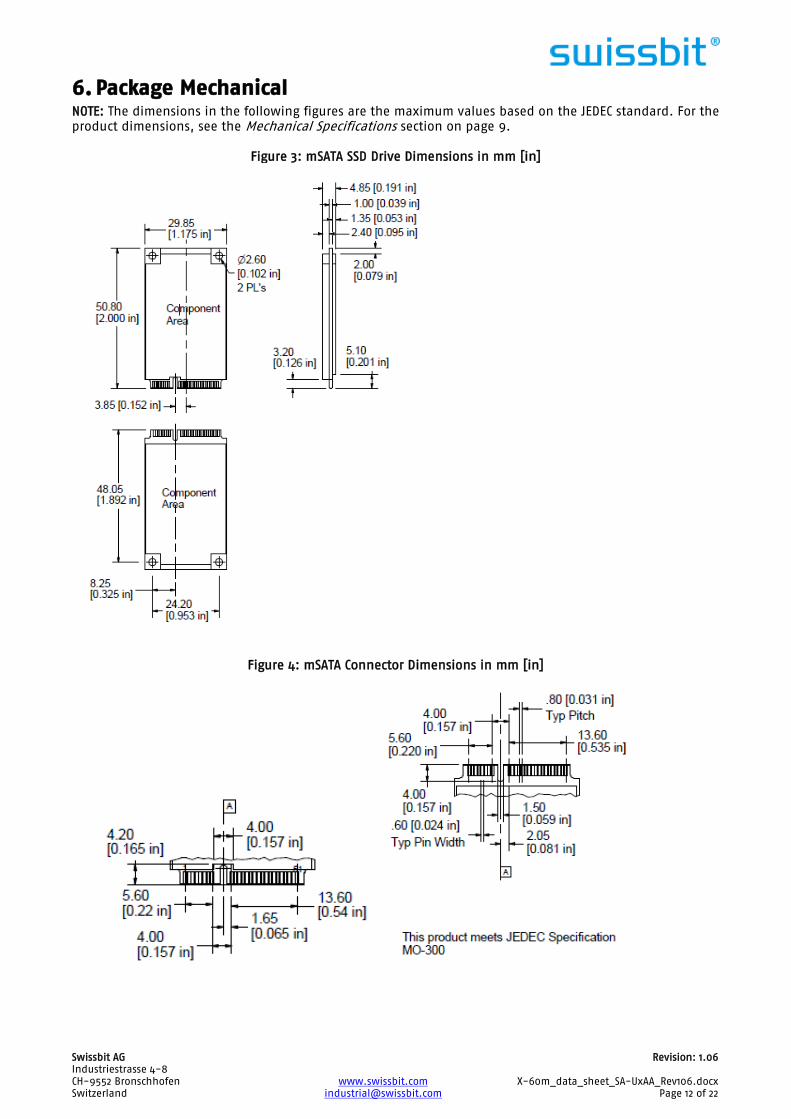
4.5 Mechanical Specifications
The X-60m SSD consists of a flash controller and NAND flash memory devices. The controller interfaces with a
host system, allowing data to be written to and read from the flash memory array. The SSD has a PCIe mini-
connector with a SATA interface. Physical dimensions are detailed in Table 9 below. Figure 3 on page 12
illustrates the X-60m dimensions and connector location.
Table 9: Measured Physical Dimensions
Physical Dimensions Unit
Length 50.80±0.15
mm Width 29.85±0.15
Thickness (Max) 3.50
Weight (Max Capacity) 7.00 g
Swissbit AG Revision: 1.06 Industriestrasse 4-8
CH-9552 Bronschhofen www.swissbit.com X-60m_data_sheet_SA-UxAA_Rev106.docx Switzerland [email protected] Page 10 of 22
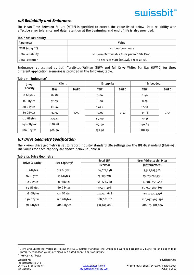
4.6 Reliability and Endurance
The Mean Time Between Failure (MTBF) is specified to exceed the value listed below. Data reliability with
effective error tolerance and data retention at the beginning and end of life is also provided.
Table 10: Reliability
Parameter Value
MTBF (at 25 °C) > 2,000,000 hours
Data Reliability < 1 Non-Recoverable Error per 1016 Bits Read
Data Retention 10 Years at Start (JESD47), 1 Year at EOL
Endurance represented as both TeraBytes Written (TBW) and full Drive Writes Per Day (DWPD) for three
different application scenarios is provided in the following table.
Table 11: Endurance7
Drive
Capacity
Client Enterprise Embedded
TBW DWPD TBW DWPD TBW DWPD
8 GBytes 16.28
1.90
4.00
0.47
4.40
0.55
16 GBytes 32.55 8.00 8.79
30 GBytes 61.04 15.00 17.58
60 GBytes 122.07 30.00 35.16
120 GBytes 244.14 59.99 70.31
240 GBytes 488.28 119.99 140.63
480 GBytes 976.56 239.97 281.25
4.7 Drive Geometry Specification
The X-60m drive geometry is set to report industry standard LBA settings per the IDEMA standard (LBA1-03).
The values for each capacity are shown below in Table 12.
Table 12: Drive Geometry
Drive Capacity User Capacity8 Total LBA User Addressable Bytes
Decimal (Unformatted)
8 GBytes 7.5 GBytes 14,672,448 7,512,293,376
16 GBytes 15 GBytes 29,323,728 15,013,748,736
32 GBytes 30 GBytes 58,626,288 30,016,659,456
64 GBytes 60 GBytes 117,231,408 60,022,480,896
128 GBytes 120 GBytes 234,441,648 120,034,123,776
256 GBytes 240 GBytes 468,862,128 240,057,409,536
512 GBytes 480 GBytes 937,703,088 480,103,981,056
7 Client and Enterprise workloads follow the JEDEC JESD219 standard; the Embedded workload creates a 4 KByte file and appends it.
Enterprise workload values are measured based on 168 hours of runtime. 8 1 GByte = 109 bytes
Swissbit AG Revision: 1.06 Industriestrasse 4-8
CH-9552 Bronschhofen www.swissbit.com X-60m_data_sheet_SA-UxAA_Rev106.docx Switzerland [email protected] Page 11 of 22
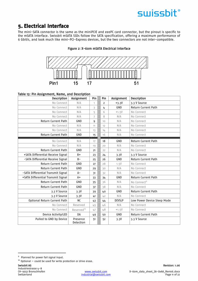
5. Electrical Interface The mini-SATA connector is the same as the miniPCIE and eeePC card connector, but the pinout is specific to
the mSATA interface. Swissbit mSATA SSDs follow the SATA specification, offering a maximum performance of
6 Gbit/s, and look much like mini-PCI-Express devices, but the two connectors are not inter-compatible.
Figure 2: X-60m mSATA Electrical Interface
Table 13: Pin Assignment, Name, and Description
Description Assignment Pin Pin Assignment Description
No Connect N/A 1 2 +3.3V 3.3 V Source
No Connect N/A 3 4 GND Return Current Path
No Connect N/A 5 6 +1.5V No Connect
No Connect N/A 7 8 N/A No Connect
Return Current Path GND 9 10 N/A No Connect
No Connect N/A 11 12 N/A No Connect
No Connect N/A 13 14 N/A No Connect
Return Current Path GND 15 16 N/A No Connect
No Connect N/A 17 18 GND Return Current Path
No Connect N/A 19 20 N/A No Connect
Return Current Path GND 21 22 N/A No Connect
+SATA Differential Receive Signal B+ 23 24 3.3V 3.3 V Source
-SATA Differential Receive Signal B- 25 26 GND Return Current Path
Return Current Path GND 27 28 1.5V No Connect
Return Current Path GND 29 30 N/A No Connect
-SATA Differential Transmit Signal A- 31 32 N/A No Connect
+SATA Differential Transmit Signal A+ 33 34 GND Return Current Path
Return Current Path GND 35 36 N/A No Connect9
Return Current Path GND 37 38 N/A No Connect
3.3 V Source 3.3V 39 40 GND Return Current Path
3.3 V Source 3.3V 41 42 N/A No Connect
Optional Return Current Path NC 43 44 DEVSLP Low Power Device Sleep Mode
No Connect Reserved 45 46 N/A No Connect
No Connect Reserved10 47 48 +1.5V No Connect
Device Activity/LED DA 49 50 GND Return Current Path
Pulled to GND by Device Presence
Detection
51 52 3.3V 3.3 V Source
9 Planned for power fail signal input. 10 Optional — could be used for write protection or drive erase.
Swissbit AG Revision: 1.06 Industriestrasse 4-8
CH-9552 Bronschhofen www.swissbit.com X-60m_data_sheet_SA-UxAA_Rev106.docx Switzerland [email protected] Page 12 of 22
6. Package Mechanical NOTE: The dimensions in the following figures are the maximum values based on the JEDEC standard. For the
product dimensions, see the Mechanical Specifications section on page 9.
Figure 3: mSATA SSD Drive Dimensions in mm [in]
Figure 4: mSATA Connector Dimensions in mm [in]
Swissbit AG Revision: 1.06 Industriestrasse 4-8
CH-9552 Bronschhofen www.swissbit.com X-60m_data_sheet_SA-UxAA_Rev106.docx Switzerland [email protected] Page 13 of 22
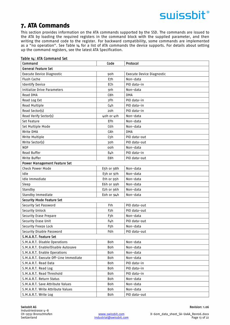
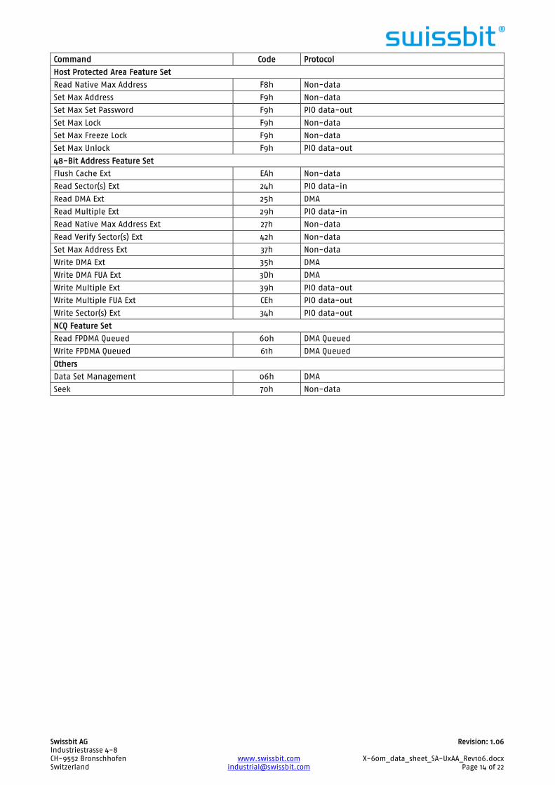
7. ATA Commands This section provides information on the ATA commands supported by the SSD. The commands are issued to
the ATA by loading the required registers in the command block with the supplied parameter, and then
writing the command code to the register. For backward compatibility, some commands are implemented
as a "no operation". See Table 14 for a list of ATA commands the device supports. For details about setting
up the command registers, see the latest ATA Specification.
Table 14: ATA Command Set
Command Code Protocol
General Feature Set
Execute Device Diagnostic 90h Execute Device Diagnostic
Flush Cache E7h Non-data
Identify Device ECh PIO data-in
Initialize Drive Parameters 91h Non-data
Read DMA C8h DMA
Read Log Ext 2Fh PIO data-in
Read Multiple C4h PIO data-in
Read Sector(s) 20h PIO data-in
Read Verify Sector(s) 40h or 41h Non-data
Set Feature EFh Non-data
Set Multiple Mode C6h Non-data
Write DMA CAh DMA
Write Multiple C5h PIO data-out
Write Sector(s) 30h PIO data-out
NOP 00h Non-data
Read Buffer E4h PIO data-in
Write Buffer E8h PIO data-out
Power Management Feature Set
Check Power Mode E5h or 98h Non-data
Idle E3h or 97h Non-data
Idle Immediate E1h or 95h Non-data
Sleep E6h or 99h Non-data
Standby E2h or 96h Non-data
Standby Immediate E0h or 94h Non-data
Security Mode Feature Set
Security Set Password F1h PIO data-out
Security Unlock F2h PIO data-out
Security Erase Prepare F3h Non-data
Security Erase Unit F4h PIO data-out
Security Freeze Lock F5h Non-data
Security Disable Password F6h PIO data-out
S.M.A.R.T. Feature Set
S.M.A.R.T. Disable Operations B0h Non-data
S.M.A.R.T. Enable/Disable Autosave B0h Non-data
S.M.A.R.T. Enable Operations B0h Non-data
S.M.A.R.T. Execute Off-Line Immediate B0h Non-data
S.M.A.R.T. Read Data B0h PIO data-in
S.M.A.R.T. Read Log B0h PIO data-in
S.M.A.R.T. Read Threshold B0h PIO data-in
S.M.A.R.T. Return Status B0h Non-data
S.M.A.R.T. Save Attribute Values B0h Non-data
S.M.A.R.T. Write Attribute Values B0h Non-data
S.M.A.R.T. Write Log B0h PIO data-out
Swissbit AG Revision: 1.06 Industriestrasse 4-8
CH-9552 Bronschhofen www.swissbit.com X-60m_data_sheet_SA-UxAA_Rev106.docx Switzerland [email protected] Page 14 of 22
Command Code Protocol
Host Protected Area Feature Set
Read Native Max Address F8h Non-data
Set Max Address F9h Non-data
Set Max Set Password F9h PIO data-out
Set Max Lock F9h Non-data
Set Max Freeze Lock F9h Non-data
Set Max Unlock F9h PIO data-out
48-Bit Address Feature Set
Flush Cache Ext EAh Non-data
Read Sector(s) Ext 24h PIO data-in
Read DMA Ext 25h DMA
Read Multiple Ext 29h PIO data-in
Read Native Max Address Ext 27h Non-data
Read Verify Sector(s) Ext 42h Non-data
Set Max Address Ext 37h Non-data
Write DMA Ext 35h DMA
Write DMA FUA Ext 3Dh DMA
Write Multiple Ext 39h PIO data-out
Write Multiple FUA Ext CEh PIO data-out
Write Sector(s) Ext 34h PIO data-out
NCQ Feature Set
Read FPDMA Queued 60h DMA Queued
Write FPDMA Queued 61h DMA Queued
Others
Data Set Management 06h DMA
Seek 70h Non-data
Swissbit AG Revision: 1.06 Industriestrasse 4-8
CH-9552 Bronschhofen www.swissbit.com X-60m_data_sheet_SA-UxAA_Rev106.docx Switzerland [email protected] Page 15 of 22
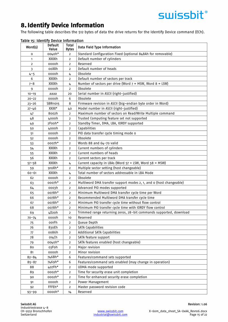
8. Identify Device Information The following table describes the 512 bytes of data the drive returns for the Identify Device command (ECh).
Table 15: Identify Device Information
Word(s) Default
Value
Total
Bytes Data Field Type Information
0 0040h* 2 Standard Configuration Fixed (optional 848Ah for removable)
1 XXXXh 2 Default number of cylinders
2 0000h 2 Reserved
3 00XXh 2 Default number of heads
4-5 0000h 4 Obsolete
6 XXXXh 2 Default number of sectors per track
7-8 XXXXh 4 Number of sectors per drive (Word 7 = MSW, Word 8 = LSW)
9 0000h 2 Obsolete
10-19 aaaa 20 Serial number in ASCII (right-justified)
20-22 0000h 6 Obsolete
23-26 SBR11015 8 Firmware revision in ASCII (big-endian byte order in Word)
27-46 XXXX* 40 Model number in ASCII (right-justified)
47 8002h 2 Maximum number of sectors on Read/Write Multiple command
48 4000h 2 Trusted Computing feature set not supported
49 2F00h* 2 Standby Timer, DMA, LBA, IORDY supported
50 4000h 2 Capabilities
51 0000h 2 PIO data transfer cycle timing mode 0
52 0000h 2 Obsolete
53 0007h* 2 Words 88 and 64-70 valid
54 XXXXh 2 Current numbers of cylinders
55 XXXXh 2 Current numbers of heads
56 XXXXh 2 Current sectors per track
57-58 XXXXh 4 Current capacity in LBAs (Word 57 = LSW, Word 58 = MSW)
59 910Xh* 2 Multiple sector setting (host changeable)
60-61 XXXXh 4 Total number of sectors addressable in LBA Mode
62 0000h 2 Obsolete
63 0007h*
0000h* 2 Multiword DMA transfer support modes 2, 1, and 0 (host changeable)
Multiword DMA not supported 64 0003h 2 Advanced PIO modes supported
65 0078h* 2 Minimum Multiword DMA transfer cycle time per Word
66 0078h* 2 Recommended Multiword DMA transfer cycle time
67 0078h* 2 Minimum PIO transfer cycle time without flow control
68 0078h* 2 Minimum PIO transfer cycle time with IORDY flow control
69 4D20h 2 Trimmed range returning zeros, 28-bit commands supported, download
microcode DMA, write/read Buffer DMA, deterministic read after TRIM 70-74 0000h 10 Reserved
75 001Fh 2 Queue Depth
76 830Eh 2 SATA Capabilities
77 0086h 2 Additional SATA Capabilities
78 014Ch 2 SATA feature support
79 0040h* 2 SATA features enabled (host changeable)
80 03F0h 2 Major revision
81 0000h 2 Minor revision
82-84 746Bh*
7701h*
4063h*
6 Features/command sets supported
85-87 7469h*
7469h*
4063h*
6 Features/command sets enabled (may change in operation)
88 407Fh* 2 UDMA mode supported
89 0002h* 2 Time for security erase unit completion
90 0002h* 2 Time for enhanced security erase completion
91 0000h 2 Power Management
92 FFFEh* 2 Master password revision code
93-99 0000h* 14 Reserved
Swissbit AG Revision: 1.06 Industriestrasse 4-8
CH-9552 Bronschhofen www.swissbit.com X-60m_data_sheet_SA-UxAA_Rev106.docx Switzerland [email protected] Page 16 of 22
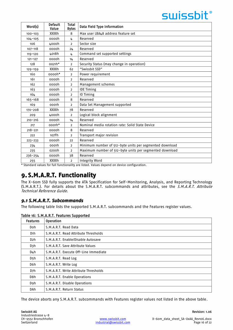
Word(s) Default
Value
Total
Bytes Data Field Type Information
100-103 XXXXh 8 Max user LBA48 address feature set
104-105 0000h 4 Reserved
106 4000h 2 Sector size
107-118 0000h 24 Reserved
119-120 4018h
4018h 4 Command set supported settings
Command set features enabled 121-127 0000h 14 Reserved
128 0021h* 2 Security Status (may change in operation)
129-159 XXXXh 62 ”Swissbit SSD”
160 0000h* 2 Power requirement
161 0000h 2 Reserved
162 0000h 2 Management schemes
163 0000h 2 IDE Timing
164 0000h 2 IO Timing
165-168 0000h 8 Reserved
169 0001h 2 Data Set Management supported
170-208 XXXXh 78 Reserved
209 4000h 2 Logical block alignment
210-216 0000h 14 Reserved
217 0001h* 2 Nominal media rotation rate: Solid State Device
218-221 0000h 8 Reserved
222 107Fh 2 Transport major revision
223-233 0000h 22 Reserved
234 0001h 2 Minimum number of 512-byte units per segmented download
235 0200h 2 Maximum number of 512-byte units per segmented download
236-254 0000h 38 Reserved
255 XXXXh 2 Integrity Word
* Standard values for full functionality are listed. Values depend on device configuration.
9. S.M.A.R.T. Functionality The X-60m SSD fully supports the ATA Specification for Self-Monitoring, Analysis, and Reporting Technology
(S.M.A.R.T.). For details about the S.M.A.R.T. subcommands and attributes, see the S.M.A.R.T. Attribute Technical Reference Guide.
9.1 S.M.A.R.T. Subcommands The following table lists the supported S.M.A.R.T. subcommands and the Features register values.
Table 16: S.M.A.R.T. Features Supported
Features Operation
D0h S.M.A.R.T. Read Data
D1h S.M.A.R.T. Read Attribute Thresholds
D2h S.M.A.R.T. Enable/Disable Autosave
D3h S.M.A.R.T. Save Attribute Values
D4h S.M.A.R.T. Execute Off-Line Immediate
D5h S.M.A.R.T. Read Log
D6h S.M.A.R.T. Write Log
D7h S.M.A.R.T. Write Attribute Thresholds
D8h S.M.A.R.T. Enable Operations
D9h S.M.A.R.T. Disable Operations
DAh S.M.A.R.T. Return Status
The device aborts any S.M.A.R.T. subcommands with Features register values not listed in the above table.
Swissbit AG Revision: 1.06 Industriestrasse 4-8
CH-9552 Bronschhofen www.swissbit.com X-60m_data_sheet_SA-UxAA_Rev106.docx Switzerland [email protected] Page 17 of 22
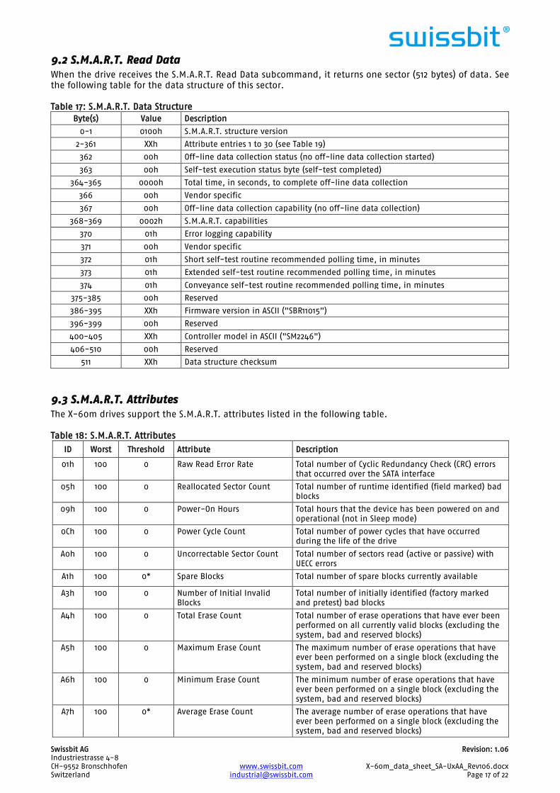
9.2 S.M.A.R.T. Read Data When the drive receives the S.M.A.R.T. Read Data subcommand, it returns one sector (512 bytes) of data. See
the following table for the data structure of this sector.
Table 17: S.M.A.R.T. Data Structure
Byte(s) Value Description
0-1 0100h S.M.A.R.T. structure version
2-361 XXh Attribute entries 1 to 30 (see Table 19)
362 00h Off-line data collection status (no off-line data collection started)
363 00h Self-test execution status byte (self-test completed)
364-365 0000h Total time, in seconds, to complete off-line data collection
366 00h Vendor specific
367 00h Off-line data collection capability (no off-line data collection)
368-369 0002h S.M.A.R.T. capabilities
370 01h Error logging capability
371 00h Vendor specific
372 01h Short self-test routine recommended polling time, in minutes
373 01h Extended self-test routine recommended polling time, in minutes
374 01h Conveyance self-test routine recommended polling time, in minutes
375-385 00h Reserved
386-395 XXh Firmware version in ASCII ("SBR11015")
396-399 00h Reserved
400-405 XXh Controller model in ASCII ("SM2246")
406-510 00h Reserved
511 XXh Data structure checksum
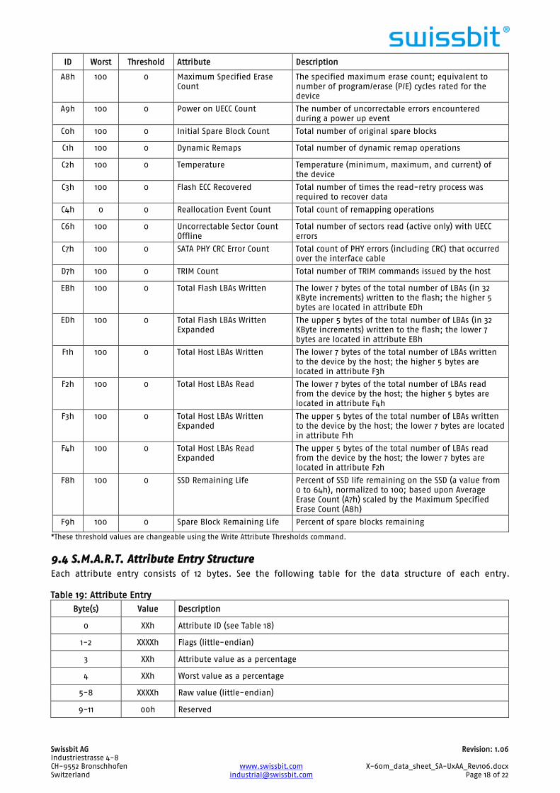
9.3 S.M.A.R.T. Attributes The X-60m drives support the S.M.A.R.T. attributes listed in the following table.
Table 18: S.M.A.R.T. Attributes
ID Worst Threshold Attribute Description
01h 100 0 Raw Read Error Rate Total number of Cyclic Redundancy Check (CRC) errors
that occurred over the SATA interface
05h 100 0 Reallocated Sector Count Total number of runtime identified (field marked) bad
blocks
09h 100 0 Power-On Hours Total hours that the device has been powered on and
operational (not in Sleep mode)
0Ch 100 0 Power Cycle Count Total number of power cycles that have occurred
during the life of the drive
A0h 100 0 Uncorrectable Sector Count Total number of sectors read (active or passive) with
UECC errors
A1h 100 0* Spare Blocks Total number of spare blocks currently available
A3h 100 0 Number of Initial Invalid
Blocks
Total number of initially identified (factory marked
and pretest) bad blocks
A4h 100 0 Total Erase Count Total number of erase operations that have ever been
performed on all currently valid blocks (excluding the
system, bad and reserved blocks)
A5h 100 0 Maximum Erase Count The maximum number of erase operations that have
ever been performed on a single block (excluding the
system, bad and reserved blocks)
A6h 100 0 Minimum Erase Count The minimum number of erase operations that have
ever been performed on a single block (excluding the
system, bad and reserved blocks)
A7h 100 0* Average Erase Count The average number of erase operations that have
ever been performed on a single block (excluding the
system, bad and reserved blocks)
Swissbit AG Revision: 1.06 Industriestrasse 4-8
CH-9552 Bronschhofen www.swissbit.com X-60m_data_sheet_SA-UxAA_Rev106.docx Switzerland [email protected] Page 18 of 22
ID Worst Threshold Attribute Description
A8h 100 0 Maximum Specified Erase
Count
The specified maximum erase count; equivalent to
number of program/erase (P/E) cycles rated for the
device
A9h 100 0 Power on UECC Count The number of uncorrectable errors encountered
during a power up event
C0h 100 0 Initial Spare Block Count Total number of original spare blocks
C1h 100 0 Dynamic Remaps Total number of dynamic remap operations
C2h 100 0 Temperature Temperature (minimum, maximum, and current) of
the device
C3h 100 0 Flash ECC Recovered Total number of times the read-retry process was
required to recover data
C4h 0 0 Reallocation Event Count Total count of remapping operations
C6h 100 0 Uncorrectable Sector Count
Offline
Total number of sectors read (active only) with UECC
errors
C7h 100 0 SATA PHY CRC Error Count Total count of PHY errors (including CRC) that occurred
over the interface cable
D7h 100 0 TRIM Count Total number of TRIM commands issued by the host
EBh 100 0 Total Flash LBAs Written The lower 7 bytes of the total number of LBAs (in 32
KByte increments) written to the flash; the higher 5
bytes are located in attribute EDh
EDh 100 0 Total Flash LBAs Written
Expanded
The upper 5 bytes of the total number of LBAs (in 32
KByte increments) written to the flash; the lower 7
bytes are located in attribute EBh
F1h 100 0 Total Host LBAs Written The lower 7 bytes of the total number of LBAs written
to the device by the host; the higher 5 bytes are
located in attribute F3h
F2h 100 0 Total Host LBAs Read The lower 7 bytes of the total number of LBAs read
from the device by the host; the higher 5 bytes are
located in attribute F4h
F3h 100 0 Total Host LBAs Written
Expanded
The upper 5 bytes of the total number of LBAs written
to the device by the host; the lower 7 bytes are located
in attribute F1h
F4h 100 0 Total Host LBAs Read
Expanded
The upper 5 bytes of the total number of LBAs read
from the device by the host; the lower 7 bytes are
located in attribute F2h
F8h 100 0 SSD Remaining Life Percent of SSD life remaining on the SSD (a value from
0 to 64h), normalized to 100; based upon Average
Erase Count (A7h) scaled by the Maximum Specified
Erase Count (A8h)
F9h 100 0 Spare Block Remaining Life Percent of spare blocks remaining
*These threshold values are changeable using the Write Attribute Thresholds command.
9.4 S.M.A.R.T. Attribute Entry Structure Each attribute entry consists of 12 bytes. See the following table for the data structure of each entry.
Table 19: Attribute Entry
Byte(s) Value Description
0 XXh Attribute ID (see Table 18)
1-2 XXXXh Flags (little-endian)
3 XXh Attribute value as a percentage
4 XXh Worst value as a percentage
5-8 XXXXh Raw value (little-endian)
9-11 00h Reserved
Swissbit AG Revision: 1.06 Industriestrasse 4-8
CH-9552 Bronschhofen www.swissbit.com X-60m_data_sheet_SA-UxAA_Rev106.docx Switzerland [email protected] Page 19 of 22
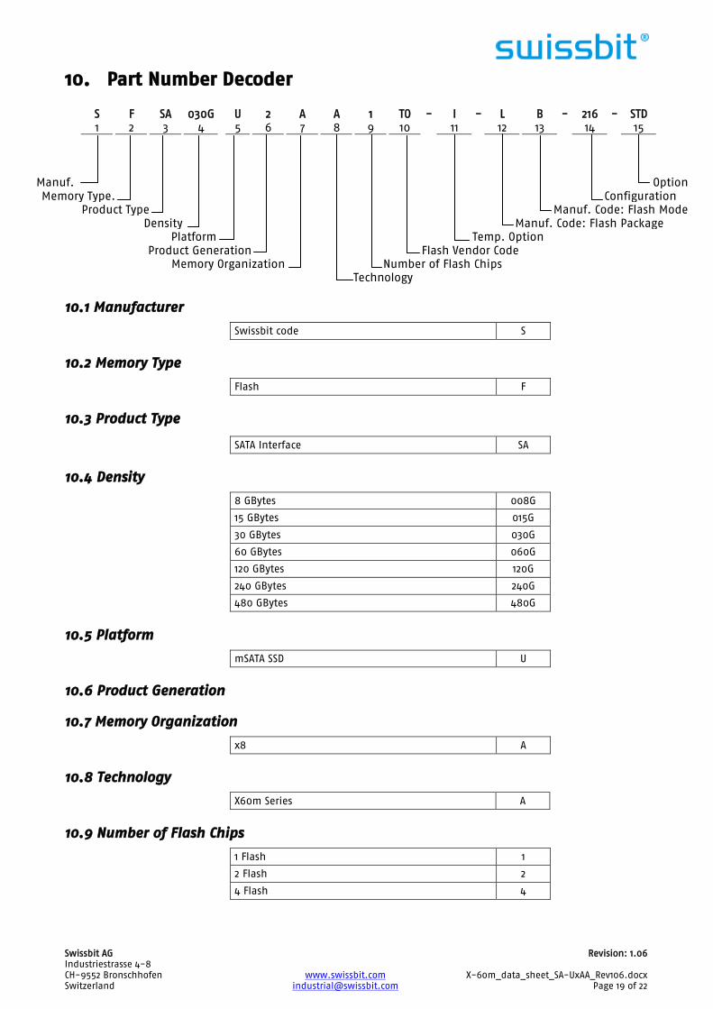
10. Part Number Decoder
S F SA 030G U 2 A A 1 TO - I - L B - 216 - STD
1 2 3 4 5 6 7 8 9 10 11 12 13 14 15
Manuf. Option
Memory Type. Configuration
Product Type Manuf. Code: Flash Mode
Density Manuf. Code: Flash Package
Platform Temp. Option
Product Generation Flash Vendor Code
Memory Organization Number of Flash Chips
Technology
10.1 Manufacturer
Swissbit code S
10.2 Memory Type
Flash F
10.3 Product Type
SATA Interface SA
10.4 Density
8 GBytes 008G
15 GBytes 015G
30 GBytes 030G
60 GBytes 060G
120 GBytes 120G
240 GBytes 240G
480 GBytes 480G
10.5 Platform
mSATA SSD U
10.6 Product Generation
10.7 Memory Organization
x8 A
10.8 Technology
X60m Series A
10.9 Number of Flash Chips
1 Flash 1
2 Flash 2
4 Flash 4
Swissbit AG Revision: 1.06 Industriestrasse 4-8
CH-9552 Bronschhofen www.swissbit.com X-60m_data_sheet_SA-UxAA_Rev106.docx Switzerland [email protected] Page 20 of 22
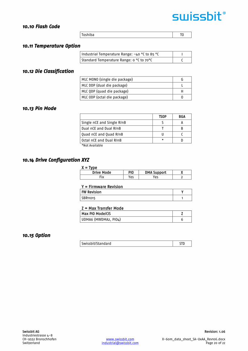
10.10 Flash Code
Toshiba TO
10.11 Temperature Option
Industrial Temperature Range: -40 °C to 85 °C I
Standard Temperature Range: 0 °C to 70°C C
10.12 Die Classification
MLC MONO (single die package) G
MLC DDP (dual die package) L
MLC QDP (quad die package) H
MLC ODP (octal die package) O
10.13 Pin Mode
TSOP BGA
Single nCE and Single R/nB S A
Dual nCE and Dual R/nB T B
Quad nCE and Quad R/nB U C
Octal nCE and Dual R/nB * D
*Not Available
10.14 Drive Configuration XYZ
X = Type Drive Mode PIO DMA Support X
Fix Yes Yes 2
Y = Firmware Revision
FW Revision Y
SBR11015 1
Z = Max Transfer Mode
Max PIO Mode/CIS Z
UDMA6 (MWDMA2, PIO4) 6
10.15 Option
Swissbit/Standard STD
Swissbit AG Revision: 1.06 Industriestrasse 4-8
CH-9552 Bronschhofen www.swissbit.com X-60m_data_sheet_SA-UxAA_Rev106.docx Switzerland [email protected] Page 21 of 22
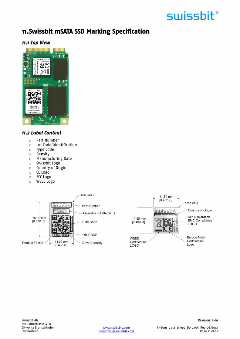
11. Swissbit mSATA SSD Marking Specification
11.1 Top View
11.2 Label Content
o Part Number
o Lot Code/Identification
o Type Code
o Density
o Manufacturing Date
o Swissbit Logo
o Country of Origin
o CE Logo
o FCC Logo
o WEEE Logo
Swissbit AG Revision: 1.06 Industriestrasse 4-8
CH-9552 Bronschhofen www.swissbit.com X-60m_data_sheet_SA-UxAA_Rev106.docx Switzerland [email protected] Page 22 of 22
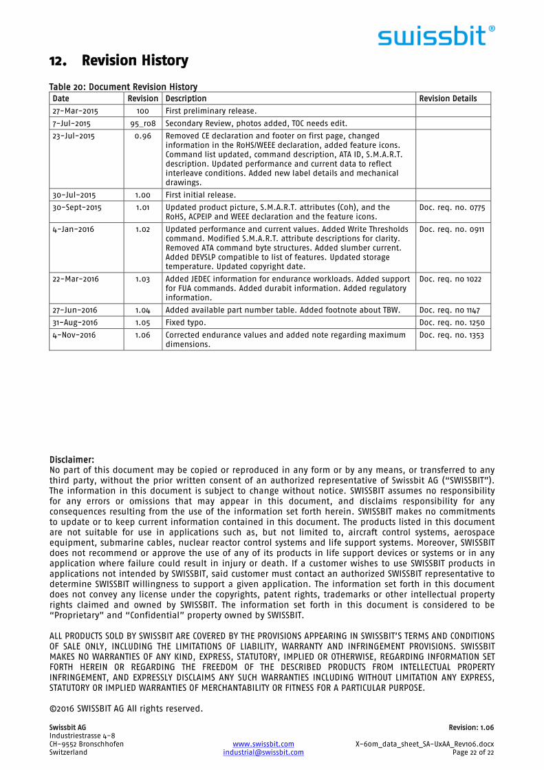
12. Revision History
Table 20: Document Revision History
Date Revision Description Revision Details
27-Mar-2015 100 First preliminary release.
7-Jul-2015 95_ro8 Secondary Review, photos added, TOC needs edit.
23-Jul-2015 0.96 Removed CE declaration and footer on first page, changed
information in the RoHS/WEEE declaration, added feature icons.
Command list updated, command description, ATA ID, S.M.A.R.T.
description. Updated performance and current data to reflect
interleave conditions. Added new label details and mechanical
drawings.
30-Jul-2015 1.00 First initial release.
30-Sept-2015 1.01 Updated product picture, S.M.A.R.T. attributes (C0h), and the
RoHS, ACPEIP and WEEE declaration and the feature icons.
Doc. req. no. 0775
4-Jan-2016 1.02 Updated performance and current values. Added Write Thresholds
command. Modified S.M.A.R.T. attribute descriptions for clarity.
Removed ATA command byte structures. Added slumber current.
Added DEVSLP compatible to list of features. Updated storage temperature. Updated copyright date.
Doc. req. no. 0911
22-Mar-2016 1.03 Added JEDEC information for endurance workloads. Added support
for FUA commands. Added durabit information. Added regulatory
information.
Doc. req. no 1022
27-Jun-2016 1.04 Added available part number table. Added footnote about TBW. Doc. req. no 1147
31-Aug-2016 1.05 Fixed typo. Doc. req. no. 1250
4-Nov-2016 1.06 Corrected endurance values and added note regarding maximum
dimensions.
Doc. req. no. 1353
Disclaimer:
No part of this document may be copied or reproduced in any form or by any means, or transferred to any
third party, without the prior written consent of an authorized representative of Swissbit AG (“SWISSBIT”).
The information in this document is subject to change without notice. SWISSBIT assumes no responsibility
for any errors or omissions that may appear in this document, and disclaims responsibility for any
consequences resulting from the use of the information set forth herein. SWISSBIT makes no commitments
to update or to keep current information contained in this document. The products listed in this document
are not suitable for use in applications such as, but not limited to, aircraft control systems, aerospace
equipment, submarine cables, nuclear reactor control systems and life support systems. Moreover, SWISSBIT
does not recommend or approve the use of any of its products in life support devices or systems or in any
application where failure could result in injury or death. If a customer wishes to use SWISSBIT products in
applications not intended by SWISSBIT, said customer must contact an authorized SWISSBIT representative to
determine SWISSBIT willingness to support a given application. The information set forth in this document
does not convey any license under the copyrights, patent rights, trademarks or other intellectual property
rights claimed and owned by SWISSBIT. The information set forth in this document is considered to be
“Proprietary” and “Confidential” property owned by SWISSBIT.
ALL PRODUCTS SOLD BY SWISSBIT ARE COVERED BY THE PROVISIONS APPEARING IN SWISSBIT’S TERMS AND CONDITIONS
OF SALE ONLY, INCLUDING THE LIMITATIONS OF LIABILITY, WARRANTY AND INFRINGEMENT PROVISIONS. SWISSBIT
MAKES NO WARRANTIES OF ANY KIND, EXPRESS, STATUTORY, IMPLIED OR OTHERWISE, REGARDING INFORMATION SET
FORTH HEREIN OR REGARDING THE FREEDOM OF THE DESCRIBED PRODUCTS FROM INTELLECTUAL PROPERTY
INFRINGEMENT, AND EXPRESSLY DISCLAIMS ANY SUCH WARRANTIES INCLUDING WITHOUT LIMITATION ANY EXPRESS,
STATUTORY OR IMPLIED WARRANTIES OF MERCHANTABILITY OR FITNESS FOR A PARTICULAR PURPOSE.
©2016 SWISSBIT AG All rights reserved.