Embed Size (px)
Citation preview
Tunnel diodeFrom Wikipedia, the free encyclopedia
Jump to: navigation, search
Tunnel diode schematic symbol
A tunnel diode or Esaki diode is a type of semiconductor diode which is capable of very fast operation, well into the microwave frequency region, by using quantum mechanical effects.
It was invented in 1958 by Leo Esaki, who in 1973 received the Nobel Prize in Physics for discovering the electron tunneling effect used in these diodes.
These diodes have a heavily doped p-n junction only some 10 nm (100 Å) wide. The heavy doping results in a broken bandgap, where conduction band electron states on the n-side are more or less aligned with valence band hole states on the p-side.
Tunnel diodes were manufactured by General Electric and other companies from about 1960, and are still made in low volume today. [1]
Contents[hide]
1 Forward bias operation 2 Reverse bias operation
3 Technical comparisons
4 References
5 See also
6 External links
[edit] Forward bias operationUnder normal forward bias operation, as voltage begins to increase, electrons at first tunnel through the very narrow p-n junction barrier because filled electron states in the conduction band on the n-side become aligned with empty valence band hole states on the p-side of the pn junction. As voltage increases further these states become more misaligned and the current drops — this is called negative resistance, because current decreases with increasing voltage. As voltage increases yet further, the diode begins to operate as a normal diode, where
1
electrons travel by conduction across the pn junction, and no longer by tunneling through the pn junction barrier. Thus the most important operating region for a tunnel diode is the negative resistance region.
[edit] Reverse bias operationWhen used in the reverse direction they are called back diodes and can act as fast rectifiers with zero offset voltage and extreme linearity for power signals. (That is, they have an accurate square law characteristic in the reverse direction.)
Under reverse bias filled states on the p-side become increasingly aligned with empty states on the n-side and electrons now tunnel through the pn junction barrier in reverse direction — this is the Zener effect that also occurs in zener diodes.
[edit] Technical comparisons
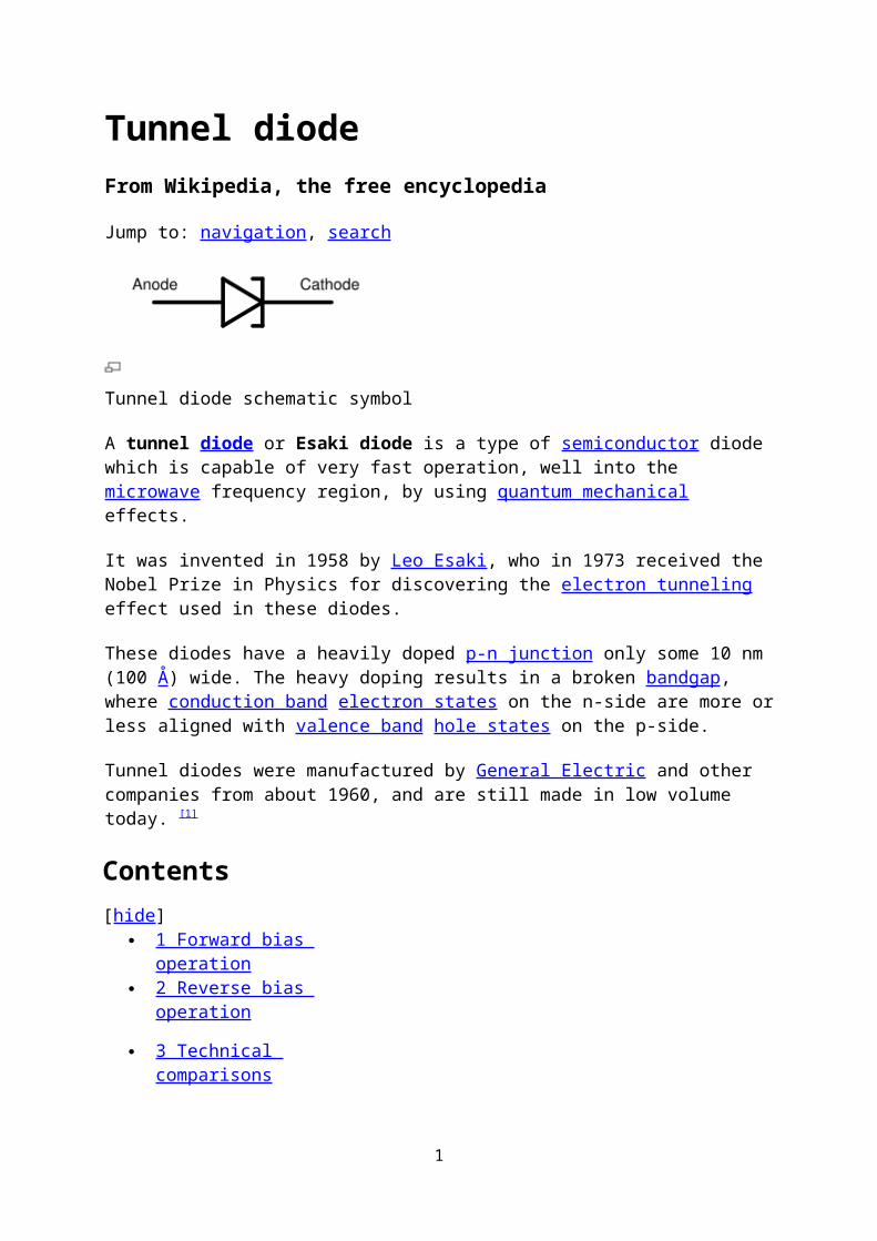
A rough approximation of the VI curve for a tunnel diode, showing the negative differential resistance region
In a conventional semiconductor diode, conduction takes place while the PN junction is forward biased and blocks current flow when the junction is reverse biased. This occurs up to a point known as the 'reverse breakdown voltage' when conduction begins (often accompanied by destruction of the device). In the tunnel diode, the dopant concentration in the P and N layers are increased to the point where the reverse breakdown voltage becomes zero and the diode conducts in the reverse direction. However, when forward-biased, an odd effect occurs called 'quantum mechanical tunnelling' which gives rise to a region where an increase in forward voltage is accompanied by a decrease in forward current. This negative resistance region can be exploited in a solid state version of the dynatron oscillator which normally uses a tetrode thermionic valve (or tube).
2
The tunnel diode showed great promise as an oscillator and high-frequency threshold (trigger) device since it would operate at frequencies far greater than the tetrode would, well into the microwave bands. Applications for tunnel diodes included local oscillators for UHF television tuners, trigger circuits in oscilloscopes, high speed counter circuits, and very fast rise time pulse generator circuits. However, since its discovery, more conventional semiconductor devices have surpassed its performance using conventional oscillator techniques. For many purposes a three-terminal device, such as a field-effect transistor, is more flexible than a device with only two terminals. Practical tunnel diodes operate at a few millamperes and a few tenths of a volt, making them low-power devices.
Tunnel diodes are also relatively resistant to nuclear radiation, as compared to other diodes. This makes them well suited to higher radiation environments, such as those found in space applications.
[edit] References1. ̂ http://www.eetimes.com/special/special_issues/millennium/milestones/
holonyak.html Tunnel diodes, the transistor killers, EE Times, retrieved 2008 April 07 ]
[edit] See also Avalanche diode Backward diode
Gunn diode
IMPATT diode
Resonant interband tunnel diode
Resonant tunnelling diode
Si/SiGe resonant tunnel diode
Si/SiGe resonant interband tunnel diode
Tunnel junction
Zener diode
[edit] External links A history of the tunnel diode and commentary on its rarity today
Retrieved from "http://en.wikipedia.org/wiki/Tunnel_diode"Categories: Diodes
3
WKB approximationFrom Wikipedia, the free encyclopedia
Jump to: navigation, search
In physics, the WKB (Wentzel-Kramers-Brillouin) approximation, also known as WKBJ (Wentzel-Kramers-Brillouin-Jeffreys) approximation, is the most familiar example of a semiclassical calculation in quantum mechanics in which the wavefunction is recast as an exponential function, semiclassically expanded, and then either the amplitude or the phase is taken to be slowly changing.
Contents[hide]
1 Brief history 2 WKB method
3 An example
4 Application to Schrödinger equation
5 See also
6 References
o 6.1 Modern references
o 6.2 Historical references
7 External links
[edit] Brief historyThis method is named after physicists Wentzel, Kramers, and Brillouin, who all developed it in 1926. In 1923, mathematician Harold Jeffreys had developed a general method of approximating linear, second-order differential equations, which includes the Schrödinger equation. But since the Schrödinger equation was developed two years later, and Wentzel, Kramers, and Brillouin were apparently unaware of this earlier work, Jeffreys is often neglected credit. Early texts in quantum mechanics contain any number of combinations of their initials, including WBK, BWK, WKBJ and BWKJ.
Earlier references to the method are: Carlini in 1817, Liouville in 1837, Green in 1837, Rayleigh in 1912 and Gans in 1915. Liouville and Green may be called the founders of the method, in 1837.The important contribution of Wentzel, Kramers, Brillouin and Jeffreys to the method was the inclusion of the treatment of turning points, connecting the evanescent and oscillatory solutions at either side of the turning point. For example, this may occur in the Schrödinger equation, due to a potential energy hill.
4
[edit] WKB methodGenerally, WKB theory is a method for approximating the solution of a differential equation whose highest derivative is multiplied by a small parameter ε. The method of approximation is as follows:
For a differential equation
assume a solution of the form of an asymptotic series expansion
In the limit . Plugging the above ansatz into the differential equation and canceling out the exponential terms will allow you to solve for an arbitrary number of terms Sn(x) in the expansion. WKB Theory is a special case of Multiple Scale Analysis.
[edit] An exampleConsider the second-order homogeneous linear differential equation
where . Plugging in
results in the equation
To leading order, (assuming, for the moment, the series will be asymptotically consistent) the above can be approximated as
In the limit , the dominant balance is given by
5
So δ is proportional to ε. Setting them equal and comparing powers renders
Which can be recognized as the Eikonal equation, with solution
Looking at first-order powers of ε gives
Which is the unidimensional transport equation, which has the solution
And k1 is an arbitrary constant. We now have a pair of approximations to the system (a pair because S0 can take two signs); the first-order WKB-approximation will be a linear combination of the two:
Higher-order terms can be obtained by looking at equations for higher powers of ε. Explicitly
for n > 2. This example comes from Bender and Orszag's textbook (see references).
[edit] Application to Schrödinger equationThe one dimensional, time-independent Schrödinger equation is
,
which can be rewritten as
.
6
The wavefunction can be rewritten as the exponential of another function Φ (which is closely related to the action):
so that
where Φ' indicates the derivative of Φ with respect to x. The derivative Φ'(x) can be separated into real and imaginary parts by introducing the real functions A and B:
The amplitude of the wavefunction is then eA(x) while the phase is B(x). The Schrödinger equation implies that these functions must satisfy:
and therefore, since the right hand side of the differential equation for Φ is real,
Next, the semiclassical approximation is invoked. This means that each function is expanded as a power series in . From the equations it can be seen that the power series must start with at least an order of to satisfy the real part of the equation. In order to achieve a good classical limit, it is necessary to start with as high a power of Planck's constant as possible.
To first order in this expansion, the conditions on A and B can be written.
If the amplitude varies sufficiently slowly as compared to the phase (A0(x) = 0), it follows that
7
which is only valid when the total energy is greater than the potential energy, as is always the case in classical motion. After the same procedure on the next order of the expansion it follows that
On the other hand, if it is the phase varies that varies slowly (as compared to the amplitude), (B0(x) = 0) then
which is only valid when the potential energy is greater than the total energy (the regime in which quantum tunneling occurs). Grinding out the next order of the expansion yields
It is apparent from the denominator, that both of these approximate solutions 'blow up' near the classical turning point where E = V(x) and cannot be valid. These are the approximate solutions away from the potential hill and beneath the potential hill. Away from the potential hill, the particle acts similarly to a free wave - the phase is oscillating. Beneath the potential hill, the particle undergoes exponential changes in amplitude.
To complete the derivation, the approximate solutions must be found everywhere and their coefficients matched to make a global approximate solution. The approximate solution near the classical turning points E = V(x) is yet to be found.
For a classical turning point x1 and close to E = V(x1), can be expanded in a power series.
To first order, one finds
This differential equation is known as the Airy equation, and the solution may be written in terms of Airy functions.
8
This solution should connect the far away and beneath solutions. Given the 2 coefficients on one side of the classical turning point, the 2 coefficients on the other side of the classical turning point can be determined by using this local solution to connect them. Thus, a relationship between C0,θ and C + ,C − can be found.
Fortunately the Airy functions will asymptote into sine, cosine and exponential functions in the proper limits. The relationship can be found to be as follows (often referred to as "connection formulas"):
Now the global (approximate) solutions can be constructed.
[edit] See also Airy Function Langer correction
Method of steepest descent / Laplace Method
Perturbation methods
Quantum tunneling
[edit] References
[edit] Modern references
Razavy, Moshen (2003). Quantum Theory of Tunneling. World Scientific. ISBN 981-238-019-1.
Griffiths, David J. (2004). Introduction to Quantum Mechanics (2nd ed.). Prentice Hall. ISBN 0-13-111892-7.
Liboff, Richard L. (2003). Introductory Quantum Mechanics (4th ed.). Addison-Wesley. ISBN 0-8053-8714-5.
Sakurai, J. J. (1993). Modern Quantum Mechanics. Addison-Wesley. ISBN 0-201-53929-2.
Bender, Carl ; Orszag, Steven (1978). Advanced Mathematical Methods for Scientists and Engineers. McGraw-Hill. ISBN 0-07-004452-X.
Olver, Frank J. W. (1974). Asymptotics and Special Functions. Academic Press. ISBN 0-12-525850-X.
9
[edit] Historical references
Carlini, Francesco (1817). Richerche sulla convergenza della serie che serva aal soluzione del problema di Keplero. Milano.
Liouville, Joseph (1837). "Sur le développement des fonctions et séries...". Journal de Mathématiques Pures et Appliquées 1: 16–35.
Green, George (1837). "On the motion of waves in a variable canal of small depth and width". Transactions of the Cambridge Philosophical Society 6: 457–462.
Rayleigh, Lord (John William Strutt) (1912). "On the propagation of waves through a stratified medium, with special reference to the question of reflection". Proceedings of the Royal Society London, Series A 86: 207–226.
Gans, Richard (1915). "Fortplantzung des Lichts durch ein inhomogenes Medium". Annalen der Physik 47: 709–736.
Jeffreys, Harold (1924). "On certain approximate solutions of linear differential equations of the second order". Proceedings of the London Mathematical Society 23: 428–436.
Brillouin, Léon (1926). "La mécanique ondulatoire de Schrödinger: une méthode générale de resolution par approximations successives". Comptes Rendus de l'Academie des Sciences 183: 24–26.
Kramers, Hendrik A. (1926). "Wellenmechanik und halbzählige Quantisierung". Zeitschrift der Physik 39: 828–840.
Wentzel, Gregor (1926). "Eine Verallgemeinerung der Quantenbedingungen für die Zwecke der Wellenmechanik". Zeitschrift der Physik 38: 518–529.
[edit] External links Richard Fitzpatrick, The W.K.B. Approximation (2002). (An application of the WKB
approximation to the scattering of radio waves from the ionosphere.) Free WKB library for Microsoft Visual C v6 for some special functions
Retrieved from "http://en.wikipedia.org/wiki/WKB_approximation"Categories: Theoretical physics | Asymptotic analysis
Scanning tunneling microscopeFrom Wikipedia, the free encyclopedia
(Redirected from Scanning tunnelling microscope)Jump to: navigation, search
10
Image of reconstruction on a clean Gold (100) surface.
STM image of self-assembled supramolecular chains of the organic semiconductor Quinacridone on Graphite.
Scanning tunneling microscopy (STM) is a powerful technique for viewing surfaces at the atomic level. Its development in 1981 won its inventors, Gerd Binnig and Heinrich Rohrer (at IBM Zürich), the Nobel Prize in Physics in 1986[1]. STM probes the density of states of a material using tunneling current. For STM, good resolution is considered to be 0.1 nm lateral resolution and 0.01 nm depth resolution[2]. The STM can be used not only in ultra high vacuum but also in air and various other liquid or gas ambients, and at temperatures ranging from near 0 Kelvin to a few hundred degrees Celsius[3].
The STM is based on the concept of quantum tunneling. When a conducting tip is brought very near to a metallic or semiconducting surface, a bias between the two can allow electrons to tunnel through the vacuum between them. For low voltages, this tunneling current is a function of the local density of states (LDOS) at the Fermi level, Ef, of the sample[3]. Variations in current as the probe passes over the surface are translated into an image. STM can be a challenging technique, as it requires extremely clean surfaces and sharp tips.
Contents[hide]
1 Tunneling 2 Procedure
3 Instrumentation
11
4 Other STM Related Studies
5 Early Invention
6 References
7 See also
8 External links
9 Literature
[edit] TunnelingTunneling is a concept that arises from quantum mechanics. Classically, an object hitting an impenetrable wall will bounce back. Imagine throwing a baseball to a friend on the other side of a mile high brick wall, directly at the wall. One would be rightfully astonished if, rather than bouncing back upon impact, the ball were to simply pass through to your friend on the other side of the wall. For objects of very small mass, as is the electron, wavelike nature has a more pronounced effect, so such an event, referred to as tunneling, has a much greater probability[3].
Electrons behave as waves of energy, and in the presence of a potential U(z), assuming 1-dimensional case, the energy levels ψn(z) of the electrons are given by solutions to Schrödinger’s equation,
,
where ħ is Planck’s constant, z is the position, and m is the mass of an electron[3]. If an electron of energy E is incident upon an energy barrier of height U(z), the electron wave function is a traveling wave solution,
,
where
if E > U(z), which is true for a wave function inside the tip or inside the sample[3]. Inside a barrier, such as between tip and sample, E < U(z) so the wave functions which satisfies this are decaying waves,
,
where
12
quantifies the decay of the wave inside the barrier, with the barrier in the +z direction for − κ [3].
Knowing the wave function allows one to calculate the probability density for that electron to be found at some location. In the case of tunneling, the tip and sample wave functions overlap such that when under a bias, there is some finite probability to find the electron in the barrier region and even on the other side of the barrier[3]. Let us assume the bias is V and the barrier width is W, as illustrated in Figure 1. This probability, P, that an electron at z=0 (left edge of barrier) can be found at z=W (right edge of barrier) is proportional to the wave function squared,
[3].
If the bias is small, we can let U − E ≈ φM in the expression for κ, where φM, the work function, gives the minimum energy needed to bring an electron from an occupied level, the highest of which is at the Fermi level (for metals at T=0 kelvins), to vacuum level. When a small bias V is applied to the system, only electronic states very near the Fermi level, within eV, are excited[3]. These excited electrons can tunnel across the barrier. In other words, tunneling occurs mainly with electrons of energies near the Fermi level.
However, tunneling does require that there is an empty level of the same energy as the electron for the electron to tunnel into on the other side of the barrier. It is because of this restriction that the tunneling current can be related to the density of available or filled states in the sample. The current due to an applied voltage V (assume tunneling occurs sample to tip) depends on two factors: 1) the number of electrons between Ef and eV in the sample, and 2) the number among them which have corresponding free states to tunnel into on the other side of the barrier at the tip[3]. The higher density of available states the greater the tunneling current. When V is positive, electrons in the tip tunnel into empty states in the sample; for a negative bias, electrons tunnel out of occupied states in the sample into the tip[3].
Mathematically, this tunneling current is given by
.
One can sum the probability over energies between Ef − eV and eV to get the number of states available in this energy range per unit volume, thereby finding the local density of states (LDOS) near the Fermi level[3]. The LDOS near some energy E in an interval ε is given by
,
and the tunnel current at a small bias V is proportional to the LDOS near the Fermi level, which gives important information about the sample[3]. It is desirable to use LDOS to express
13
the current because this value does not change as the volume changes, while probability density does[3]. Thus the tunneling current is given by
where ρs(0,Ef) is the LDOS near the Fermi level of the sample at the sample surface[3]. By using equation (6), this current can also be expressed in terms of the LDOS near the Fermi level of the sample at the tip surface,
The exponential term in (9) is very significant in that small variations in W greatly influence the tunnel current. If the separation is decreased by 1 Ǻ, the current increases by an order of magnitude, and vice versa[4].
This approach fails to account for the rate at which electrons can pass the barrier. This rate should affect the tunnel current, so it can be accounted for by using Fermi’s Golden Rule with the appropriate tunneling matrix element. John Bardeen solved this problem in his study of the metal-insulator-metal junction, MIM[5]. He found that if he solved Schrödinger’s equation for each side of the junction separately to obtain the wave functions ψ and χ for each electrode, he could obtain the tunnel matrix, M, from the overlap of these two wave functions[3]. This can be applied to STM by making the electrodes the tip and sample, assigning ψ and χ as sample and tip wave functions, respectively, and evaluating M at some surface S between the metal electrodes at z=zo, where z=0 at the sample surface and z=W at the tip surface[3].
Now, Fermi’s Golden Rule gives the rate for electron transfer across the barrier, and is written
,
where δ(Eψ-Eχ) restricts tunneling to occur only between electron levels with the same energy[3]. The tunnel matrix element, given by
,
is a description of the lower energy associated with the interaction of wave functions at the overlap, also called the resonance energy[3].
Summing over all the states gives the tunneling current as
,
14
where f is the Fermi function, ρs and ρT are the density of states in the sample and tip, respectively[3]. The Fermi distribution function describes the filling of electron levels at a given temperature T.
[edit] ProcedureFirst the tip is brought into close proximity of the sample by some coarse sample-to-tip control. The values for common sample-to-tip distance, W, range from about 4-7 Ǻ, which is the equilibrium position between attractive (3<W<10Ǻ) and repulsive (W<3Ǻ) interactions[3]. Once tunneling is established, piezoelectric transducers are implemented to move the tip in three directions. As the tip is rastered across the sample in the x-y plane, the density of states and therefore the tunnel current changes. This change in current with respect to position can be measured itself, or the height, z, of the tip corresponding to a constant current can be measured[3]. These two modes are called constant height mode and constant current mode, respectively.
In constant current mode, feedback electronics adjust the height by a voltage to the piezoelectric height control mechanism[6]. This leads to a height variation and thus the image comes from the tip topography across the sample and gives a constant charge density surface; this means contrast on the image is due to variations in charge density[4].
In constant height, the voltage and height are both held constant while the current changes to keep the voltage from changing; this leads to an image made of current changes over the surface, which can be related to charge density[4]. The benefit to using a constant height mode is that it is faster, as the piezoelectric movements require more time to register the change in constant current mode than the voltage response in constant height mode[4].
In addition to scanning across the sample, information on the electronic structure of the sample can be obtained by sweeping voltage and measuring current at a specific location[2]. This type of measurement is called scanning tunneling spectroscopy (STS).
[edit] Instrumentation
15
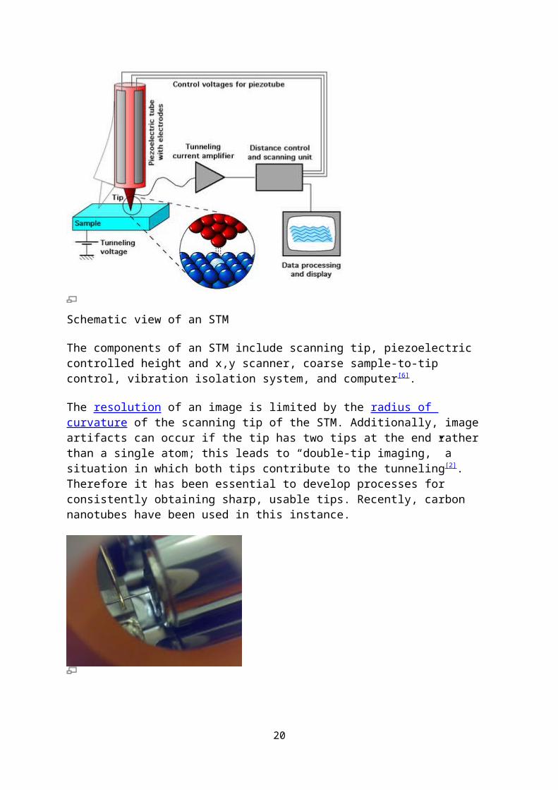
Schematic view of an STM
The components of an STM include scanning tip, piezoelectric controlled height and x,y scanner, coarse sample-to-tip control, vibration isolation system, and computer[6].
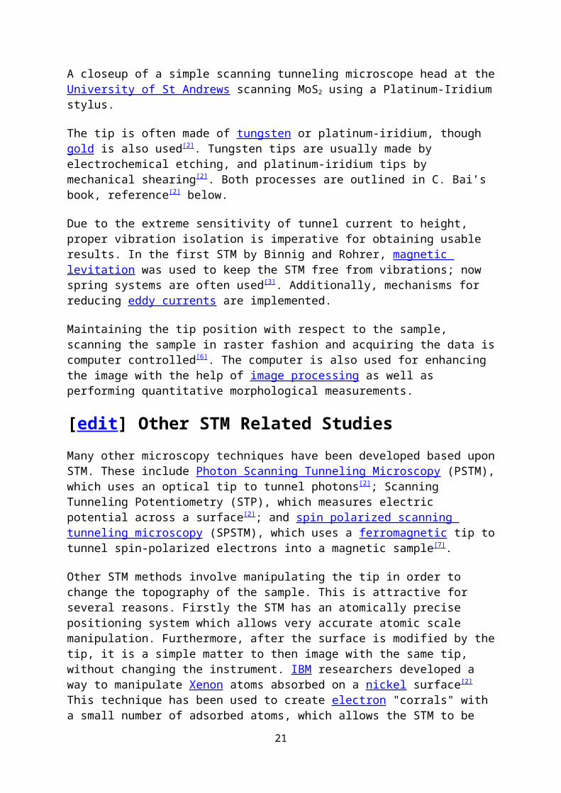
The resolution of an image is limited by the radius of curvature of the scanning tip of the STM. Additionally, image artifacts can occur if the tip has two tips at the end rather than a single atom; this leads to “double-tip imaging,” a situation in which both tips contribute to the tunneling[2]. Therefore it has been essential to develop processes for consistently obtaining sharp, usable tips. Recently, carbon nanotubes have been used in this instance.
A closeup of a simple scanning tunneling microscope head at the University of St Andrews scanning MoS2 using a Platinum-Iridium stylus.
The tip is often made of tungsten or platinum-iridium, though gold is also used[2]. Tungsten tips are usually made by electrochemical etching, and platinum-iridium tips by mechanical shearing[2]. Both processes are outlined in C. Bai’s book, reference[2] below.
Due to the extreme sensitivity of tunnel current to height, proper vibration isolation is imperative for obtaining usable results. In the first STM by Binnig and Rohrer, magnetic
16
levitation was used to keep the STM free from vibrations; now spring systems are often used[3]. Additionally, mechanisms for reducing eddy currents are implemented.
Maintaining the tip position with respect to the sample, scanning the sample in raster fashion and acquiring the data is computer controlled[6]. The computer is also used for enhancing the image with the help of image processing as well as performing quantitative morphological measurements.
[edit] Other STM Related StudiesMany other microscopy techniques have been developed based upon STM. These include Photon Scanning Tunneling Microscopy (PSTM), which uses an optical tip to tunnel photons[2]; Scanning Tunneling Potentiometry (STP), which measures electric potential across a surface[2]; and spin polarized scanning tunneling microscopy (SPSTM), which uses a ferromagnetic tip to tunnel spin-polarized electrons into a magnetic sample[7].
Other STM methods involve manipulating the tip in order to change the topography of the sample. This is attractive for several reasons. Firstly the STM has an atomically precise positioning system which allows very accurate atomic scale manipulation. Furthermore, after the surface is modified by the tip, it is a simple matter to then image with the same tip, without changing the instrument. IBM researchers developed a way to manipulate Xenon atoms absorbed on a nickel surface[2] This technique has been used to create electron "corrals" with a small number of adsorbed atoms, which allows the STM to be used to observe electron Friedel Oscillations on the surface of the material. Aside from modifying the actual sample surface, one can also use the STM to tunnel electrons into a layer of E-Beam photoresist on a sample, in order to do lithography. This has the advantage of offering more control of the exposure than traditional Electron beam lithography.
Recently groups have found they can use the STM tip to rotate individual bonds within single molecules. The electrical resistance of the molecule depends on the orientation of the bond, so the molecule effectively becomes a molecular switch.
[edit] Early InventionAn early, patented invention, based on the above-mentioned principles, and later acknowledged by the Nobel committeee itself, was the Topografiner of R. Young, J. Ward, and F. Scire from the NIST ("National Institute of Science and Technolology" of the USA)[8].
[edit] References1. ̂ G. Binnig, H. Rohrer “Scanning tunneling microscopy” IBM Journal of Research
and Development 30,4 (1986) reprinted 44,½ Jan/Mar (2000)2. ^ a b c d e f g h i C. Bai Scanning tunneling microscopy and its applications Springer
Verlag, 2nd edition, New York (1999)
3. ^ a b c d e f g h i j k l m n o p q r s t u v w C. Julian Chen Introduction to Scanning Tunneling Micro scopy(1993)
17
4. ^ a b c d D. A. Bonnell and B. D. Huey “Basic principles of scanning probe microscopy” from Scanning probe microscopy and spectroscopy: Theory, techniques, and applications 2nd edition Ed. By D. A. Bonnell Wiley-VCH, Inc. New York (2001)
5. ̂ J. Bardeen “Tunneling from a many particle point of view” Phys. Rev. Lett. 6,2 57-59 (1961)
6. ^ a b c K. Oura, V. G. Lifshits, A. A. Saranin, A. V. Zotov, and M. Katayama Surface science: an introduction Springer-Verlag Berlin (2003)
7. ̂ R. Wiesendanger, I. V. Shvets, D. Bürgler, G. Tarrach, H.-J. Güntherodt, and J.M.D. Coey “Recent advances in spin-polarized scanning tunneling microscopy” Ultramicroscopy 42-44 (1992)
8. ̂ R. Young, J. Ward, F. Scire, The Topografiner: An Instrument for Measuring Surface Topography, Rev. Sci. Instrum. 43, 999 (1972)
[edit] See also
Wikibooks' [[wikibooks:|]] has more about this subject: The Opensource Handbook of Nanoscience and Nanotechnology
Wikimedia Commons has media related to: Scanning tunneling microscope
Part of a series of articles on
Nanotechnology
HistoryImplicationsApplications
OrganizationsIn fiction and popular culture
List of topicsSubfields and related fields
NanomaterialsFullerenes
Carbon nanotubesNanoparticles
NanomedicineNanotoxicology
NanosensorMolecular self-assemblySelf-assembled monolayer
18
Supramolecular assemblyDNA nanotechnology
NanoelectronicsMolecular electronics
NanocircuitryNanolithography
Scanning probe microscopyAtomic force microscope
Scanning tunneling microscopeMolecular nanotechnology
Molecular assemblerNanorobotics
MechanosynthesisThis box: view • talk • edit
Microscopy Scanning probe microscopy
Scanning tunneling spectroscopy
Electrochemical scanning tunneling microscope
Atomic force microscope
Electron microscope
Spin polarized scanning tunneling microscopy
[edit] External links Scanning Electron Microscope is filming a STM (mpeg movie 3MB) Zooming into the Nanoworld (Animation with measured STM images)
SPM - Scanning Probe Microscopy Website
STM Image Gallery at IBM Almaden Research Center
STM Gallery at Vienna University of technology
Build a simple STM with a cost of materials less than $100.00 excluding oscilloscope
Nanotimes Simulation engine download page
[edit] Literature Tersoff, J.: Hamann, D. R.: Theory of the scanning tunneling microscope, Physical
Review B 31, 1985, p. 805 - 813. Bardeen, J.: Tunnelling from a many-particle point of view, Physical Review Letters 6
(2), 1961, p. 57-59.
Chen, C. J.: Origin of Atomic Resolution on Metal Surfaces in Scanning Tunneling Microscopy, Physical Review Letters 65 (4), 1990, p. 448-451
19
G. Binnig, H. Rohrer, Ch. Gerber, and E. Weibel, Phys. Rev. Lett. 50, 120 - 123 (1983)
G. Binnig, H. Rohrer, Ch. Gerber, and E. Weibel, Phys. Rev. Lett. 49, 57 - 61 (1982)
G. Binnig, H. Rohrer, Ch. Gerber, and E. Weibel, Appl. Phys. Lett., Vol. 40, Issue 2, pp. 178-180 (1982)
R. V. Lapshin, Feature-oriented scanning methodology for probe microscopy and nanotechnology, Nanotechnology, volume 15, issue 9, pages 1135-1151, 2004
[hide]
v • d • e
Scanning probe microscopyCommon Atomic force · Scanning tunneling
Other
Electrostatic force · Electrochemical scanning tunneling · Kelvin probe force · Magnetic force · Magnetic resonance force · Near-field scanning optical · Photothermal microspectroscopy · Scanning capacitance · Scanning gate · Scanning Hall probe · Scanning ion-conductance · Spin polarized scanning tunneling · Scanning voltage
ApplicationsScanning probe lithography · Dip-Pen Nanolithography · Feature-oriented scanning · IBM Millipede
See also Nanotechnology · Microscope · MicroscopyRetrieved from "http://en.wikipedia.org/wiki/Scanning_tunneling_microscope"Categories: Scanning probe microscopy | Swiss inventions
Finite potential barrier (QM)From Wikipedia, the free encyclopedia
In quantum mechanics, the finite potential barrier is a standard one-dimensional problem that demonstrates the phenomenon of quantum tunnelling. The problem consists of solving the time-independent Schrödinger equation for a particle with a finite size barrier potential in one dimension. Typically, a free particle impinges on the barrier from the left.
20
Although classically the particle would be reflected, quantum mechanics states that there is a finite probability that the particle will penetrate the barrier and continue travelling through to the other side. The likelihood that the particle will pass through the barrier is given by the transmission coefficient, while the likelihood that it is reflected is given by the reflection coefficient.
Contents[hide]
1 Calculation 2 E = V 0
3 Transmission and reflection
4 Analysis of the obtained expressions
o 4.1 E < V 0
o 4.2 E > V 0
o 4.3 E = V 0
5 Remarks and applications
6 See also
7 References
8 External links
[edit] CalculationThe time-independent Schrödinger equation for the wave function ψ(x) reads
where H is the Hamiltonian, is the (reduced) Planck constant, m is the mass, E the energy of the particle and
V(x) = V0[Θ(x) − Θ(x − a)]
21
Scattering at a finite potential barrier of height V0. The amplitudes and direction of left and right moving waves are indicated. In red, those waves used for the derivation of the reflection and transmission amplitude. E > V0 for this illustration.
is the barrier potential with height V0 > 0 and width a. is the Heaviside step function. The barrier is
positioned between x = 0 and x = a. Without changing the results, any other shifted position
was possible. The first term in the Hamiltonian, is the kinetic energy.
The barrier divides the space in three parts (x < 0,0 < x < a,x > 0). In any of these parts the potential is constant meaning the particle is quasi-free, and the solution of the Schrödinger equation can be written as a superposition of left and right moving waves (see free particle). If E > V0
,
, and
where the wave numbers are related to the energy via
.
The index r/l on the coefficients A and B denotes the direction of the velocity vector. Note that if the energy of the particle is below the barrier height, k1 becomes imaginary and the wave function is exponentially decaying within the barrier. Nevertheless we keep the notation
22

r/l even though the waves are not propagating anymore in this case. Here we assumed . The case E = V0 is treated below.
The coefficients A,B,C have to be found from the boundary conditions of the wave function at x = 0 and x = a. The wave function and its derivative have to be continuous everywhere, so.
ψL(0) = ψC(0),
,ψC(a) = ψR(a),
.
Inserting the wave functions, the boundary conditions give the following restrictions on the coefficients
Ar + Al = Br + Bl
ik0(Ar − Al) = ik1(Br − Bl),
,
.
[edit] E = V0
If the energy equals the barrier height, the solutions of the Schrödinger equation in the barrier region are not exponentials anymore but linear functions of the space coordinate
The complete solution of the Schrödinger equation is found in the same way as above by matching wave functions and their derivatives at x = 0 and x = a. That results in the following restrictions on the coefficients:
Ar + Al = B1
ik0(Ar − Al) = B2,
,
.
[edit] Transmission and reflectionAt this point, it is instructive to compare the situation to the classical case. In both cases, the particle behaves as a free particle outside of the barrier region. A classical particle with energy E larger than the barrier height V0 would always pass the barrier, and a classical particle with E < V0 incident on the barrier would always get reflected.
To study the quantum case, consider the following situation: a particle incident on the barrier from the left side (Ar). It may be reflected (Al) or transmitted (Cr).
23
To find the amplitudes for reflection and transmission for incidence from the left, we put in the above equations Ar = 1 (incoming particle), Al = r (reflection), Cl=0 (no incoming particle from the right) and Cr = t (transmission). We then eliminate the coefficients Bl,Br from the equation and solve for r,t.
The result is:
Due to the mirror symmetry of the model, the amplitudes for incidence from the right are the same as those from the left. Note that these expressions hold for any energy E > 0.
[edit] Analysis of the obtained expressions
[edit] E < V0
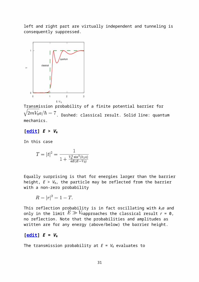
The surprising result is that for energies less than the barrier height, E < V0 there is a non-zero probability
for the particle to be transmitted through the barrier, being . This effect which differs from the classical case is called quantum tunneling. The transmission is exponentially suppressed with the barrier width which can be understood from the functional form of the wave function: outside of the barrier it oscillates with wave vector k0, while within the barrier it is exponentially damped over a distance 1 / k1. If the barrier is much larger than this decay length, the left and right part are virtually independent and tunneling is consequently suppressed.
24
Transmission probability of a finite potential barrier for . Dashed: classical result. Solid line: quantum mechanics.
[edit] E > V0
In this case
Equally surprising is that for energies larger than the barrier height, E > V0, the particle may be reflected from the barrier with a non-zero probability
This reflection probability is in fact oscillating with k1a and only in the limit approaches the classical result r = 0, no reflection. Note that the probabilities and amplitudes as written are for any energy (above/below) the barrier height.
[edit] E = V0
The transmission probability at E = V0 evaluates to
.
[edit] Remarks and applicationsThe calculation presented above may at first seem unrealistic and hardly useful. However it has proved to be a suitable model for a variety of real-life systems. One such example are interfaces between two conducting materials. In the bulk of the materials, the motion of the
25
electrons is quasi free and can be described by the kinetic term in the above Hamiltonian with an effective mass m. Often the surfaces of such materials are covered with oxide layers or are not ideal for other reasons. This thin, non-conducting layer may then be modeled by a barrier potential as above. Electrons may then tunnel from one material to the other giving rise to a current.
The operation of a scanning tunneling microscope (STM) relies on this tunneling effect. In that case the barrier is due to the air between the tip of the STM and the underlying object. Since the tunnel current depends exponentially on the barrier width, this device is extremely sensitive to height variations on the examined sample.
The above model is one-dimensional while space is three-dimensional. One should solve the Schrödinger equation in three dimensions. On the other hand, many systems only change along one coordinate direction and are translationally invariant along the others. The Schrödinger equation may then be reduced to the case considered here by an ansatz for the wave function of the type: Ψ(x,y,z) = ψ(x)φ(y,z).
For another, related model of a barrier see Delta potential barrier (QM) which can be regarded as a special case of the finite potential barrier. All results from this article immediately apply to the delta potential barrier taking the limits while keeping
constant.
[edit] See also Pauli exclusion principle
[edit] References Griffiths, David J. (2004). Introduction to Quantum Mechanics (2nd ed.). Prentice
Hall. ISBN 0-13-111892-7. Claude Cohen-Tannoudji, Bernard Diu et Frank Laloë (1977). Mécanique quantique,
vol. I et II. Paris: Collection Enseignement des sciences (Hermann). ISBN 2-7056-5767-3.
[edit] External linksRetrieved from "http://en.wikipedia.org/wiki/Finite_potential_barrier_%28QM%29"Categories: Quantum mechanics
Flash memoryFrom Wikipedia, the free encyclopedia
Jump to: navigation, search
26
This article needs additional citations for verification.Please help improve this article by adding reliable references. Unsourced material may be challenged and removed. (April 2008)
Computer memory typesVolatile
DRAM , e.g. DDR SDRAM
SRAM
Upcoming
o Z-RAM
o TTRAM
Historical
o Williams tube
o Delay line memory Non-volatile
ROM
o PROM
o EAROM
o EPROM
o EEPROM
Flash memory
Upcoming
o FeRAM
o MRAM
o Memristor
o PRAM
o SONOS
o RRAM
o Racetrack memory
o NRAM
Historical
o Drum memory
27
o Magnetic core memory
o Bubble memory
o Twistor memory
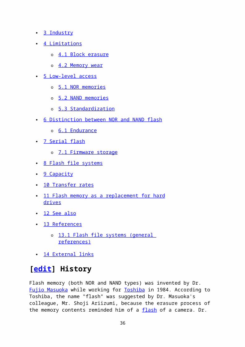
A USB flash drive. The chip on the left is the flash memory. The microcontroller is on the right.
Flash memory is non-volatile computer memory that can be electrically erased and reprogrammed. It is a technology that is primarily used in memory cards and USB flash drives for general storage and transfer of data between computers and other digital products. It is a specific type of EEPROM (Electrically Erasable Programmable Read-Only Memory) that is erased and programmed in large blocks; in early flash the entire chip had to be erased at once. Flash memory costs far less than byte-programmable EEPROM and therefore has become the dominant technology wherever a significant amount of non-volatile, solid-state storage is needed. Example applications include PDAs (personal digital assistants), laptop computers, digital audio players, digital cameras and mobile phones. It has also gained popularity in the game console market, where it is often used instead of EEPROMs or battery-powered SRAM for game save data.
Flash memory is non-volatile, which means that no power is needed to maintain the information stored in the chip. In addition, flash memory offers fast read access times (although not as fast as volatile DRAM memory used for main memory in PCs) and better kinetic shock resistance than hard disks. These characteristics explain the popularity of flash memory in portable devices. Another feature of flash memory is that when packaged in a "memory card," it is enormously durable, being able to withstand intense pressure, extremes of temperature, and even immersion in water.
Although technically a type of EEPROM, the term "EEPROM" is generally used to refer specifically to non-flash EEPROM which is erasable in small blocks, typically bytes. Because erase cycles are slow, the large block sizes used in flash memory erasing give it a significant speed advantage over old-style EEPROM when writing large amounts of data.
Contents[hide]
1 History 2 Principles of operation
o 2.1 NOR flash
28
o 2.2 NAND flash
3 Industry
4 Limitations
o 4.1 Block erasure
o 4.2 Memory wear
5 Low-level access
o 5.1 NOR memories
o 5.2 NAND memories
o 5.3 Standardization
6 Distinction between NOR and NAND flash
o 6.1 Endurance
7 Serial flash
o 7.1 Firmware storage
8 Flash file systems
9 Capacity
10 Transfer rates
11 Flash memory as a replacement for hard drives
12 See also
13 References
o 13.1 Flash file systems (general references)
14 External links
[edit] HistoryFlash memory (both NOR and NAND types) was invented by Dr. Fujio Masuoka while working for Toshiba in 1984. According to Toshiba, the name "flash" was suggested by Dr. Masuoka's colleague, Mr. Shoji Ariizumi, because the erasure process of the memory contents reminded him of a flash of a camera. Dr. Masuoka presented the invention at the IEEE 1984 International Electron Devices Meeting (IEDM) held in San Francisco, California. Intel saw the massive potential of the invention and introduced the first commercial NOR type flash chip in 1988.
NOR-based flash has long erase and write times, but provides full address and data buses, allowing random access to any memory location. This makes it a suitable replacement for older ROM chips, which are used to store program code that rarely needs to be updated, such
29
as a computer's BIOS or the firmware of set-top boxes. Its endurance is 10,000 to 1,000,000 erase cycles.[citation needed] NOR-based flash was the basis of early flash-based removable media; CompactFlash was originally based on it, though later cards moved to less expensive NAND flash.
Toshiba announced NAND flash at ISSCC in 1989. It has faster erase and write times, and requires a smaller chip area per cell, thus allowing greater storage densities and lower costs per bit than NOR flash; it also has up to ten times the endurance of NOR flash. However, the I/O interface of NAND flash does not provide a random-access external address bus. Rather, data must be read on a block-wise basis, with typical block sizes of hundreds to thousands of bits. This made NAND flash unsuitable as a drop-in replacement for program ROM since most microprocessors and microcontrollers required byte-level random access. In this regard NAND flash is similar to other secondary storage devices such as hard disks and optical media, and is thus very suitable for use in mass-storage devices such as memory cards. The first NAND-based removable media format was SmartMedia, and many others have followed, including MultiMediaCard, Secure Digital, Memory Stick and xD-Picture Card. A new generation of memory card formats, including RS-MMC, miniSD and microSD, and Intelligent Stick, feature extremely small form factors. For example, the microSD card has an area of just over 1.5 cm², with a thickness of less than 1 mm; microSD capacities range from 64MB to 16GB, as of March 2008.[citation needed]
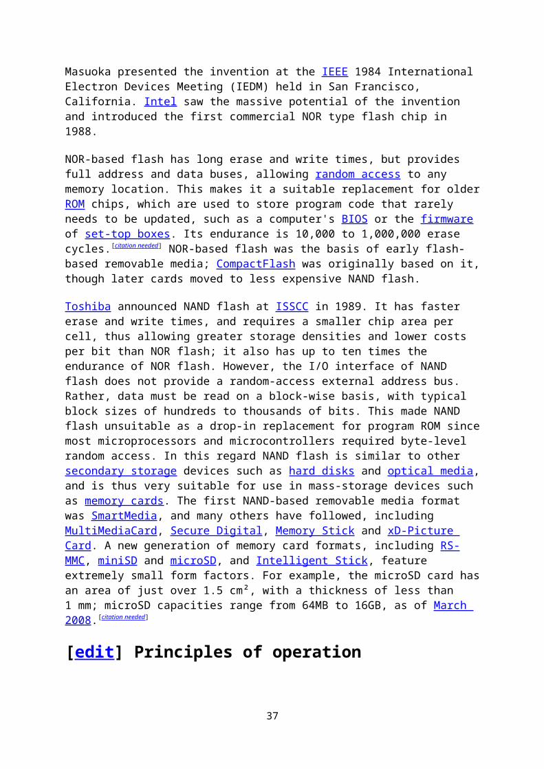
[edit] Principles of operationFlash memory stores information in an array of memory cells made from floating-gate transistors. In traditional single-level cell (SLC) devices, each cell stores only one bit of information. Some newer flash memory, known as multi-level cell (MLC) devices, can store more than one bit per cell by choosing between multiple levels of electrical charge to apply to the floating gates of its cells.
A flash memory cell.
[edit] NOR flash
30
Programming a NOR memory cell (setting it to logical 0), via hot-electron injection.
Erasing a NOR memory cell (setting it to logical 1), via quantum tunneling.
In NOR gate flash, each cell resembles a standard MOSFET, except the transistor has two gates instead of one. On top is the control gate (CG), as in other MOS transistors, but below this there is a floating gate (FG) insulated all around by an oxide layer. The FG is interposed between the CG and the MOSFET channel. Because the FG is electrically isolated by its insulating layer, any electrons placed on it are trapped there and, under normal conditions, will not discharge for many years. When the FG holds a charge, it screens (partially cancels) the electric field from the CG, which modifies the threshold voltage (VT) of the cell. During read-out, a voltage is applied to the CG, and the MOSFET channel will become conducting or remain insulating, depending on the VT of the cell, which is in turn controlled by charge on the FG. The current flow through the MOSFET channel is sensed and forms a binary code, reproducing the stored data. In a multi-level cell device, which stores more than one bit per cell, the amount of current flow is sensed (rather than simply its presence or absence), in order to determine more precisely the level of charge on the FG.
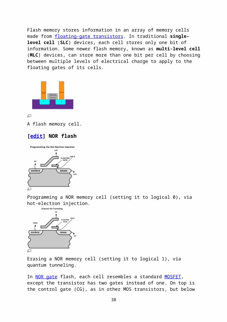
A single-level NOR flash cell in its default state is logically equivalent to a binary "1" value, because current will flow through the channel under application of an appropriate voltage to the control gate. A NOR flash cell can be programmed, or set to a binary "0" value, by the following procedure:
an elevated on-voltage (typically >5 V) is applied to the CG the channel is now turned on, so electrons can flow between the source and the drain
the source-drain current is sufficiently high to cause some high energy electrons to jump through the insulating layer onto the FG, via a process called hot-electron injection
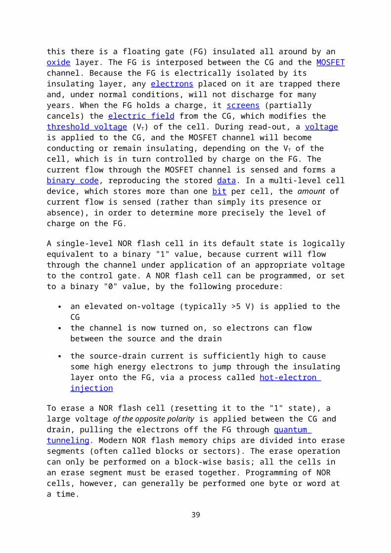
To erase a NOR flash cell (resetting it to the "1" state), a large voltage of the opposite polarity is applied between the CG and drain, pulling the electrons off the FG through quantum tunneling. Modern NOR flash memory chips are divided into erase segments (often called blocks or sectors). The erase operation can only be performed on a block-wise basis; all the cells in an erase segment must be erased together. Programming of NOR cells, however, can generally be performed one byte or word at a time.
Despite the need for high programming and erasing voltages, virtually all flash chips today require only a single supply voltage, and produce the high voltages via on-chip charge pumps.
31
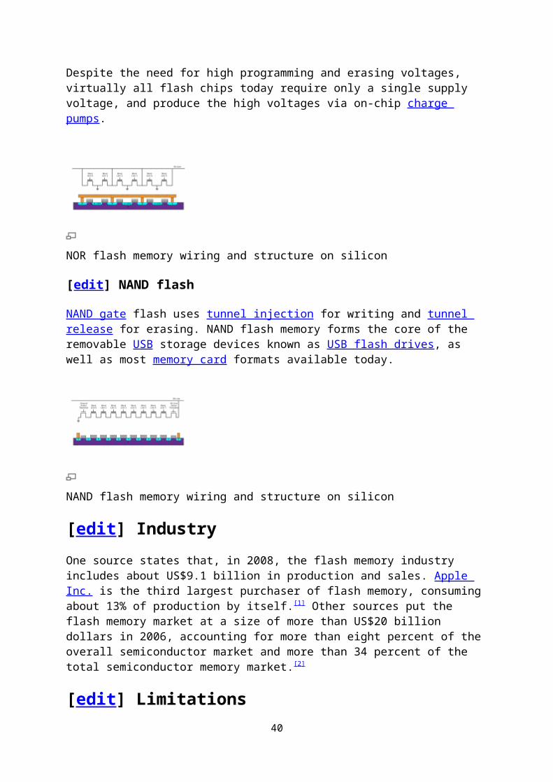
NOR flash memory wiring and structure on silicon
[edit] NAND flash
NAND gate flash uses tunnel injection for writing and tunnel release for erasing. NAND flash memory forms the core of the removable USB storage devices known as USB flash drives, as well as most memory card formats available today.
NAND flash memory wiring and structure on silicon
[edit] IndustryOne source states that, in 2008, the flash memory industry includes about US$9.1 billion in production and sales. Apple Inc. is the third largest purchaser of flash memory, consuming about 13% of production by itself.[1] Other sources put the flash memory market at a size of more than US$20 billion dollars in 2006, accounting for more than eight percent of the overall semiconductor market and more than 34 percent of the total semiconductor memory market.[2]
[edit] Limitations
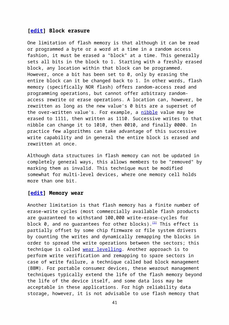
[edit] Block erasure
One limitation of flash memory is that although it can be read or programmed a byte or a word at a time in a random access fashion, it must be erased a "block" at a time. This generally sets all bits in the block to 1. Starting with a freshly erased block, any location within that block can be programmed. However, once a bit has been set to 0, only by erasing the entire block can it be changed back to 1. In other words, flash memory (specifically NOR flash) offers random-access read and programming operations, but cannot offer arbitrary random-access rewrite or erase operations. A location can, however, be rewritten as long as the new value's 0 bits are a superset of the over-written value's. For example, a nibble value may be erased to 1111, then written as 1110. Successive writes to that nibble can change it to
32
1010, then 0010, and finally 0000. In practice few algorithms can take advantage of this successive write capability and in general the entire block is erased and rewritten at once.
Although data structures in flash memory can not be updated in completely general ways, this allows members to be "removed" by marking them as invalid. This technique must be modified somewhat for multi-level devices, where one memory cell holds more than one bit.
[edit] Memory wear
Another limitation is that flash memory has a finite number of erase-write cycles (most commercially available flash products are guaranteed to withstand 100,000 write-erase-cycles for block 0, and no guarantees for other blocks).[3] This effect is partially offset by some chip firmware or file system drivers by counting the writes and dynamically remapping the blocks in order to spread the write operations between the sectors; this technique is called wear levelling. Another approach is to perform write verification and remapping to spare sectors in case of write failure, a technique called bad block management (BBM). For portable consumer devices, these wearout management techniques typically extend the life of the flash memory beyond the life of the device itself, and some data loss may be acceptable in these applications. For high reliability data storage, however, it is not advisable to use flash memory that has been through a large number of programming cycles. This limitation does not apply to 'read-only' applications such as thin clients and routers, which are only programmed once or at most a few times during their lifetime.
[edit] Low-level accessThe low-level interface to flash memory chips usually differs from those of other common types such as DRAM, ROM, and EEPROM, which support random-access via externally accessible address buses.
While NOR memory provides an external address bus for read operations (and thus supports random-access), unlocking, erasing, and writing NOR memory must proceed on a block-by-block basis. Typical block sizes are 64, 128, or 256 bytes. With NAND flash memory, all operations must be performed in a block-wise fashion: reading, unlocking, erasing, and writing.
[edit] NOR memories
Reading from NOR flash is similar to reading from random-access memory, provided the address and data bus are mapped correctly. Because of this, most microprocessors can use NOR flash memory as execute in place (XIP) memory, meaning that programs stored in NOR flash can be executed directly without the need to copy them into RAM. NOR flash chips lack intrinsic bad block management, so when a flash block is worn out, the software or device driver controlling the device must handle this, or the device will cease to work reliably.
When unlocking, erasing or writing NOR memories, special commands are written to the first page of the mapped memory. These commands are defined by the Common Flash memory Interface (CFI) and the flash chips can provide a list of available commands to the physical driver.
33
Apart from being used as random-access ROM, NOR memories can also be used as storage devices. However, NOR flash chips typically have slow write speeds compared with NAND flash.
[edit] NAND memories
NAND flash architecture was introduced by Toshiba in 1989. These memories are accessed much like block devices such as hard disks or memory cards. Each block consists of a number of pages. The pages are typically 512 or 2,048 or 4,096 bytes in size. Associated with each page are a few bytes (typically 12–16 bytes) that should be used for storage of an error detection and correction checksum.
Typical block sizes include:32 pages of 512 bytes each for a block size of 16 kiB64 pages of 2,048 bytes each for a block size of 128 kiB64 pages of 4,096 bytes each for a block size of 256 kiB
While programming is performed on a page basis, erasure can only be performed on a block basis.
NAND devices also require bad block management by the device driver software, or by a separate controller chip. SD cards, for example, include controller circuitry to perform bad block management and wear leveling. When a logical block is accessed by high-level software, it is mapped to a physical block by the device driver or controller, and a number of blocks on the flash chip are set aside for storing mapping tables to deal with bad blocks. The overall memory capacity gradually shrinks as more blocks are marked as bad.
The error-correcting and detecting checksum will typically correct an error where one bit per 256 bytes (2,048 bits) is incorrect. When this happens, the block is marked bad in a logical block allocation table, and its undamaged contents are copied to a new block and the logical block allocation table is altered accordingly. If more than one bit out of 2,048 is corrupted, the contents are partly lost, i.e. it is no longer possible to reconstruct the original contents. If this is detected when the block is written, the contents may still be available.
Most NAND devices are shipped from the factory with some bad blocks which are typically identified and marked according to a specified bad block marking strategy. By allowing some bad blocks, the manufacturers achieve far higher yields than would be possible if all blocks were tested good. This significantly reduces NAND flash costs and only slightly decreases the storage capacity of the parts.
The first physical block (block 0) is always guaranteed to be readable and free from errors. Hence, all vital pointers for partitioning and bad block management for the device must be located inside this block (typically a pointer to the bad block tables etc). If the device is used for booting a system, this block may contain the master boot record.
When executing software from NAND memories, virtual memory strategies are often used: memory contents must first be paged or copied into memory-mapped RAM and executed there. A memory management unit (MMU) in the system is helpful, but this can also be accomplished with overlays. For this reason, some systems will use a combination of NOR and NAND memories, where a smaller NOR memory is used as software ROM and a larger
34
NAND memory is partitioned with a file system for use as a random access storage area. NAND is best suited to flash devices requiring high capacity data storage. This type of flash architecture combines higher storage space with faster erase, write, and read capabilities over the execute in place advantage of the NOR architecture.
[edit] Standardization
A group called the Open NAND Flash Interface Working Group (ONFI) has developed a standardized low-level interface for NAND flash chips. This allows interoperability between conforming NAND devices from different vendors. The ONFI specification version 1.0[4] was released on December 28, 2006. It specifies:
a standard physical interface (pinout) for NAND flash in TSOP-48, WSOP-48, LGA-52, and BGA-63 packages
a standard command set for reading, writing, and erasing NAND flash chips
a mechanism for self-identification (comparable to the Serial Presence Detection feature of SDRAM chips)
The ONFI group is supported by major NAND flash manufacturers, including Intel, Micron Technology, and Sony, as well as by major manufacturers of devices incorporating NAND flash chips.[5]
A group of vendors, including Intel, Dell, and Microsoft formed a Non-Volatile Memory Host Controller Interface (NVMHCI) Working Group.[6] The goal of the group is to provide standard software and hardware programming interfaces for nonvolatile memory subsystems, including the "flash cache" device connected to the PCI Express bus.
[edit] Distinction between NOR and NAND flashNOR and NAND flash differ in two important ways:
the connections of the individual memory cells are different the interface provided for reading and writing the memory is different (NOR allows
random-access for reading, NAND allows only page access)
It is important to understand that these two are linked by the design choices made in the development of NAND flash. An important goal of NAND flash development was to reduce the chip area required to implement a given capacity of flash memory, and thereby to reduce cost per bit and increase maximum chip capacity so that flash memory could compete with magnetic storage devices like hard disks.
NOR and NAND flash get their names from the structure of the interconnections between memory cells.[7] In NOR flash, cells are connected in parallel to the bit lines, allowing cells to be read and programmed individually. The parallel connection of cells resembles the parallel connection of transistors in a CMOS NOR gate. In NAND flash, cells are connected in series, resembling a NAND gate, and preventing cells from being read and programmed individually: the cells connected in series must be read in series.
35
When NOR flash was developed, it was envisioned as a more economical and conveniently rewritable ROM than contemporary EPROM, EAROM, and EEPROM memories. Thus random-access reading circuitry was necessary. However, it was expected that NOR flash ROM would be read much more often than written, so the write circuitry included was fairly slow and could only erase in a block-wise fashion; random-access write circuitry would add to the complexity and cost unnecessarily.
Because of the series connection, a large grid of NAND flash memory cells will occupy only a small fraction of the area of equivalent NOR cells (assuming the same CMOS process resolution, e.g. 130 nm, 90 nm, 65 nm). NAND flash's designers realized that the area of a NAND chip, and thus the cost, could be further reduced by removing the external address and data bus circuitry. Instead, external devices could communicate with NAND flash via sequential-accessed command and data registers, which would internally retrieve and output the necessary data. This design choice made random-access of NAND flash memory impossible, but the goal of NAND flash was to replace hard disks, not to replace ROMs.
[edit] Endurance
The endurance of NAND flash is much greater than that of NOR flash (typically 1,000,000 cycles vs. 100,000 cycles). This is because programming and erasure in NOR flash rely on different submicroscopic processes (hot electron injection), while they are perfectly symmetric in NAND flash (Fowler-Nordheim tunneling).[7] The asymmetric nature of NOR flash programming and erasure increases the rate at which memory cells degrade, over many program/erase cycles.
The superior symmetric programming method of NAND flash has in fact been adopted in many NOR flash designs, so that some modern NOR chips boast endurance comparable to NAND flash.[7]
[edit] Serial flashSerial flash is a small, low-power flash memory that uses a serial interface, typically SPI, for sequential data access. When incorporated into an embedded system, serial flash requires fewer wires on the PCB than parallel flash memories, since it transmits and receives data one bit at a time. This may permit a reduction in board space, power consumption, and total system cost.
There are several reasons why a serial device, with fewer external pins than a parallel device, can significantly reduce overall cost:
Many ASICs are pad-limited, meaning that the size of the die is constrained by the number of wire bond pads, rather than the complexity and number of gates used for the device logic. Eliminating bond pads thus permits a more compact integrated circuit, on a smaller die; this increases the number of dies that may be fabricated on a wafer, and thus reduces the cost per die.
Reducing the number of external pins also reduces assembly and packaging costs. A serial device may be packaged in a smaller and simpler package than a parallel device.
Smaller and lower pin-count packages occupy reduced PCB area.
36
Lower pin-count devices simplify PCB routing.
[edit] Firmware storage
With the increasing speed of modern CPUs, parallel flash devices are often too slow to execute in place program code stored on them. Conversely, modern SRAM offers access times below 10 ns, while DDR2 SDRAM offers access times below 20 ns. Because of this, it is often necessary to shadow code stored in flash into RAM; that is, code must be copied from flash into RAM before execution, so that the CPU may access it at full speed. Device firmware may be stored in a serial flash device, and then copied into SDRAM or SRAM when the device is powered-up.[8] Using an external serial flash device rather than on-chip flash removes the need for significant process compromise (a process that is good for high speed logic is generally not good for flash and vice-versa). Once it is decided to read the firmware in as one big block it is common to add compression to allow a smaller flash chip to be used. Typical applications for serial flash include storing firmware for hard drives, Ethernet controllers, DSL modems, wireless network devices, etc.
[edit] Flash file systemsBecause of the particular characteristics of flash memory, it is best used with either a controller to perform wear-levelling and error correction or specifically designed file systems which spread writes over the media and deal with the long erase times of NOR flash blocks. The basic concept behind flash file systems is: When the flash store is to be updated, the file system will write a new copy of the changed data over to a fresh block, remap the file pointers, then erase the old block later when it has time.
One of the earliest flash file systems was Microsoft's FFS2 (presumably preceded by FFS1), for use with MS-DOS in the early 1990s.[9]
Around 1994, the PCMCIA, an industry group, approved the Flash Translation Layer (FTL) specification, which allowed a Linear Flash device to look like a FAT disk, but still have effective wear levelling. Other commercial systems such as FlashFX and FlashFX Pro by Datalight were created to avoid patent concerns with FTL.
JFFS was the first flash-specific file system for Linux, but it was quickly superseded by JFFS2, originally developed for NOR flash. Then YAFFS was released in 2002, dealing specifically with NAND flash, and JFFS2 was updated to support NAND flash too.
In practice, flash file systems are only used for "Memory Technology Devices" ("MTD"), which are embedded flash memories that do not have a controller. Removable flash memory cards and USB flash drives have built-in controllers to perform wear-levelling and error correction so use of a specific flash file system does not add any benefit. These removable flash memory devices use the FAT file system to allow universal compatibility with computers, cameras, PDAs and other portable devices with memory card slots or ports.
[edit] CapacityMultiple chips are often arrayed to achieve higher capacities for use in consumer electronic devices such as multimedia player or GPS. The capacity of flash chips generally follows
37
Moore's Law because they are manufactured with many of the same integrated circuits techniques and equipments.
Consumer flash drives typically have sizes measured in powers of two (e.g. 512 MB, 8 GB), but unlike DIMMs (and like hard drives) these sizes use decimal units.
In 2005, Toshiba and SanDisk developed a NAND flash chip capable of storing 1 GB of data using Multi-level Cell (MLC) technology, capable of storing 2 bits of data per cell. In September 2005, Samsung Electronics announced that it had developed the world’s first 2 GB chip.[10]
In March 2006, Samsung announced flash hard drives with a capacity of 4 GB, essentially the same order of magnitude as smaller laptop hard drives, and in September 2006, Samsung announced an 8 GB chip produced using a 40 nanometer manufacturing process.[11]
In January 2008 Sandisk announced availability of their 12GB MicroSDHC and 32GB SDHC Plus cards. [12][13]
[edit] Transfer ratesCommonly advertised is the maximum read speed, nand flash memory cards are generally faster at reading than writing.
Transferring multiple small files, smaller than the chip specific block size, could lead to much lower rate.
Access latency has an influence on performance but is less of an issue than with their hard drive counterpart.
Sometime denoted in MB/s (megabyte per second) or in number of "X" like 60x 100x or 150x. "X" speed rating makes reference to the speed at which a legacy audio CD drive would deliverer data, 1x is equal to 150 kibibytes per second.
For example a 100x memory card goes to 150 KiB x 100 = 15000 KiB per second = 14.65 MiB per second.Note: The exact speed depends on which definition of "megabyte" the marketer has chosen to use.
[edit] Flash memory as a replacement for hard drivesMain article: Solid-state drive
An obvious extension of flash memory would be as a replacement for hard disks. Flash memory does not have the mechanical limitations and latencies of hard drives, so the idea of a solid-state drive, or SSD, is attractive when considering speed, noise, power consumption, and reliability.
There remain some aspects of flash-based SSDs that make the idea unattractive. Most importantly, the cost per gigabyte of flash memory remains significantly higher than that of platter-based hard drives. Although this ratio is decreasing rapidly for flash memory, it is not
38
yet clear that flash memory will catch up to the capacities and affordability offered by platter-based storage. Still, research and development is sufficiently vigorous that it is not clear that it will not happen, either.[citation needed]
There is also some concern that the finite number of erase/write cycles of flash memory would render flash memory unable to support an operating system. This seems to be a decreasing issue as warranties on flash-based SSDs are approaching those of current hard drives.[14][15]
As of May 24, 2006, South Korean consumer-electronics manufacturer Samsung Electronics had released the first flash-memory based PCs, the Q1-SSD and Q30-SSD, both of which have 32 GB SSDs.[16] Dell Computer introduced the Latitude D430 laptop with 32 GB flash-memory storage in July 2007 -- at a price significantly above a hard-drive equipped version.[citation needed]
At the Las Vegas CES 2007 Summit Taiwanese memory company A-DATA showcased SSD hard disk drives based on Flash technology in capacities of 32 GB, 64 GB and 128 GB.[17] Sandisk announced an OEM 32 GB 1.8" SSD drive at CES 2007.[18] The XO-1, developed by the One Laptop Per Child (OLPC) association, uses flash memory rather than a hard drive. As of June 2007, a South Korean company called Mtron claims the fastest SSD with sequential read/write speeds of 100 MB/80 MB per second.[19]
Rather than entirely replacing the hard drive, hybrid techniques such as hybrid drive and ReadyBoost attempt to combine the advantages of both technologies, using flash as a high-speed cache for files on the disk that are often referenced, but rarely modified, such as application and operation system executable files. Also, Addonics has a PCI adapter for 4 CF cards,[20] creating a RAID-able array of solid-state storage that is much cheaper than the hardwired-chips PCI card kind.
The ASUS Eee PC uses a flash-based SSD of 2GB, 4GB or 8GB capacity, depending on model. The Apple Inc. Macbook Air has the option to upgrade the standard hard drive to a 64GB Solid State hard drive. The Lenovo ThinkPad X300 also features a built-in 64GB Solid State Drive.
[edit] See also List of emerging technologies CompactFlash
Wear levelling
DataFlash
Open NAND Flash Interface Working Group
YAFFS
1T-FLASH
[edit] References
39
1. ̂ Deffree, Suzanne (4 2008). "Apple sneezes, flash industry gets sick". EDN 2008 (7): 74. Retrieved on 2008-04-19.
2. ̂ Yinug, Christopher Falan (7 2007). "The Rise of the Flash Memory Market: Its Impact on Firm Behavior and Global Semiconductor Trade Patterns". Journal of International Commerce and Economics. Retrieved on 2008-04-19.
3. ̂ lwn.net/Articles/234441/.
4. ̂ www.onfi.org/docs/ONFI_1_0_Gold.pdf (PDF).
5. ̂ A list of ONFI members is available at http://www.onfi.org/onfimembers.html.
6. ̂ www.intel.com/pressroom/archive/releases/20070530corp.htm.
7. ^ a b c See pages 5-7 of Toshiba's "NAND Applications Design Guide" under External links.
8. ̂ Many serial flash devices implement a bulk read mode and incorporate an internal address counter, so that it is trivial to configure them to transfer their entire contents to RAM on power-up. When clocked at 50 MHz, for example, a serial flash could transfer a 64 Mbit firmware image in less than two seconds.
9. ̂ Microsoft FFS2 patent
10. ̂ www.xbitlabs.com/news/memory/display/20050912212649.html.
11. ̂ www.tgdaily.com/content/view/28504/135/.
12. ̂ 12GB MicroSDHC
13. ̂ [ http://www.sandisk.com/Corporate/PressRoom/PressReleases/PressRelease.aspx?ID=4091 32GB SDHC Plus]
14. ̂ www.storagesearch.com/semico-art1.html.
15. ̂ www.storagesearch.com/bitmicro-art1.html.
16. ̂ www.samsung.com/he/presscenter/pressrelease/pressrelease_20060524_0000257996.asp.
17. ̂ Future of Flash revealed.
18. ̂ SanDisk SSD Solid State Drives.
19. ̂ http://www.mtron.net/eng/index.asp
20. ̂ Addonics PCI adapter for 4 CF cards.
Digital Memories Survive Extremes
Flash memory database
[edit] Flash file systems (general references)
40
Presentation on various Flash File Systems - 9/24/2007 Article regarding various Flash File Systems - 2005 USENIX Annual Conference
Survey of various Flash File Systems - 8/10/2005
[edit] External links Open NAND Flash Interface Working Group A Nonvolatile Memory Overview
How Flash Memory Works
SanDisk Flash Memory Plant
What is NAND Flash
NAND Flash Applications
NAND Flash Applications Design Guide from Toshiba (explains the low-level details of interfacing with common NAND flash chips)
NAND vs. NOR Flash Memory from Toshiba
Samsung Develops New Flash Memory Chip - AP, October 23, 2007
Retrieved from "http://en.wikipedia.org/wiki/Flash_memory"Categories: Solid-state computer storage media | Computer memory | Non-volatile memory
Delta potential wellFrom Wikipedia, the free encyclopedia
(Redirected from Delta potential barrier (QM))Jump to: navigation, search
This article does not cite any references or sources. (April 2008)Please help improve this article by adding citations to reliable sources. Unverifiable material may be challenged and removed.
The Delta potential well is a common theoretical problem of quantum mechanics. It consists of a time-independent Schrödinger equation for a particle in a potential well defined by a delta function in one dimension.
Contents[hide]
1 Calculation 2 Transmission and Reflection
o 2.1 E > 0
41
3 Bound state
o 3.1 E < 0
4 Remarks
5 delta function potential
o 5.1 Bound solution
o 5.2 Derivation of bound solution
o 5.3 Left side of the potential
o 5.4 Right side of the potential
o 5.5 Energy of the bound state
o 5.6 Normalization
6 Delta potential barrier
o 6.1 Calculation
o 6.2 Transmission and reflection
o 6.3 Remarks, Application
7 See also
[edit] CalculationThe time-independent Schrödinger equation for the wave function ψ(x) is
where H is the Hamiltonian, is the (reduced) Planck constant, m is the mass, E the energy of the particle, and
is the delta function well with strength λ < 0. The potential is located at the origin. Without changing the results, any other shifted position was possible.
The potential well splits the space in two parts (x < 0,x > 0). In any of these parts the potential energy is constant, and the solution of the Schrödinger equation can be written as a superposition of exponentials:
42
, and
where the wave vector is related to the energy via
The index r/l on the coefficients A and B denotes the direction of the velocity vector (for E > 0). Even though the association with propagating waves only holds for positive energies (real wave vectors), the same notation is used for E < 0. The coefficients A,B have to be determined from the boundary conditions of the wave function at x = 0:
ψL = ψR,
.
The second of these equations follows from integrating the Schrödinger equation with respect to x in the vicinity of x=0. The boundary conditions thus give the following restrictions on the coefficients
Ar + Al = Br + Bl
[edit] Transmission and Reflection
43
[edit] E > 0
For positive energies, the particle is free to move in either half-space: x < 0,x > 0. It may be scattered at the delta-function well. The calculation is identical to the one in Delta potential barrier (QM) the only difference being that λ is now negative.
The quantum case can be studied in the following situation: a particle incident on the barrier from the left side (Ar). It may be reflected (Al) or transmitted (Br). To find the amplitudes for reflection and transmission for incidence from the left, put in the above equations Ar = 1 (incoming particle), Al = r (reflection), Bl=0 (no incoming particle from the right) and Br = t (transmission) and solve for r,t. The result is:
Due to the mirror symmetry of the model, the amplitudes for incidence from the right are the same as those from the left. The result is that there is a non-zero probability
for the particle to be reflected from the barrier. This is a purely quantum effect which does not appear in the classical case.
Taking this to conclusion, the probability for transmission is:
.
44
Transmission (T) and reflection (R) probability of a delta potential well. The energy E > 0 is
in units of . Dashed: classical result. Solid line: quantum mechanics.
[edit] Bound state
[edit] E < 0
In any one-dimensional attractive potential there will be a bound state. To find its energy, note
that for E<0, is complex and the wave functions which were oscillating for positive energies in the calculation above, are now exponentially increasing or decreasing functions of x (see above). Requiring that the wave functions do not diverge at eliminates half of the terms: Ar = Bl = 0. The wave function is then
, and
.
From the first of the above boundary conditions, it follows Al = Br and from the second there obtains a relation between k and the well strength λ
.
The energy of the bound state is then
.
[edit] RemarksThe delta function potential well is a special case of the finite potential well and follows as a limit of infinite depth and zero width of the well, keeping the product of width and depth constant equal to λ2 / m2.
[edit] delta function potentialThe delta function potential provides a simple example of a situation that can be solved with the Schrödinger equation. It is a one-dimensional potential and is given by:
That is, it is a potential well which is zero everywhere except at x = 0.
[edit] Bound solution
45
The graph of the bound state wavefunction solution to the delta function potential is continuous everywhere, but its derivative is not at x=0.
When the potential is of the form above, the solution of the Schrödinger equation shows that the bound state wavefunction is:
And the energy can have only one value, and that is:
[edit] Derivation of bound solution
We are interested in finding the wave function for a bound state of this delta function potential. The wave function will be a solution to the Schrödinger equation:
where
is the mass of the particleis the (complex valued) wavefunction
that we want to find
is a function describing the potential at each point x and
is the energy, a real number.
In this case V is this delta function potential mentioned above, and it divides the space into two regions. As it will turn out, the solution to the Schrödinger equation will be a different function on each side:
But one should expect a symmetrical answer for a bound state, and that will be shown to be true.
46
[edit] Left side of the potential
In the region to the left of the delta function, the potential is zero so the Schrödinger equation takes the form:
Rearranging this,
Now, for a bound state the energy, E, of the particle must be less than zero. So to make it more clear what the solution will be, write this as:
The solution to differential equations of this form involve the exponential:
where in this situation,
We can eliminate the second term in ψ1 because in this left-hand region it would blow up as x approaches .
So, in this region,
[edit] Right side of the potential
In the region to the right of the potential, the Schrödinger equation takes on the same form in the previous section,
The only difference now is we have to keep the exponentially decreasing term - the other one would blow up as x approaches .
So,
47
[edit] Energy of the bound state
So far, it has been shown that the solution must have the form
.where
, andA and B are yet to be determined.
One can find out more about the solution by applying two important rules about wavefunctions:
A wavefunction, ψ, must be continuous everywhere and
Its derivatives, , must be continuous except where the potential blows up (goes to infinity).
Putting the first rule into math:
Therefore,
The last trick, is to integrate the Schrödinger equation around x=0, but do so over a really small range:
where ε is a really small number.
The right-hand side is
and this is a more accurate approximation the smaller ε is. In the limit of this just goes to 0.
The left-hand side is
48
Which, after rearranging is
.
Let ε get closer and closer to zero, and remember that to the left of the delta potential ψ = ψ1 and on the right of it ψ = ψ2:
Thus we have a relationship between the constant c in the wavefunction and the "strength" of the delta function potential:
But don't forget that c is related to the energy, so plugging that in,
This condition shows the one allowed energy, which is:
[edit] Normalization
Finally, to figure out what the constant A out front of the wavefunction is, one can normalize the wavefunction (i.e. make sure the probability of finding the particle somewhere equals 1):
This has to equal one, so
49
This can be plugged back into the wavefunction and we find:
.
Which can be written more compactly as
[edit] Delta potential barrierThe Delta potential barrier is a textbook problem of quantum mechanics. The problem consists of solving the time-independent Schrödinger equation for a particle in a delta function potential in one dimension.
Scattering at a delta function potential of strength λ. The amplitudes and direction of left and right moving waves are indicated. In red, those waves used for the derivation of the reflection and transmission amplitude.
[edit] Calculation
The time-independent Schrödinger equation for the wave function ψ(x) reads
where H is the Hamiltonian, is the (reduced) Planck constant, m is the mass, E the energy of the particle and
50
is the delta function potential (barrier) with strength λ > 0. Here we have chosen the potential to be at the origin. Without changing the results, any other shifted position was possible. The
first term in the Hamiltonian, is the kinetic energy.
The barrier divides the space in two parts (x < 0,x > 0). In any of these parts the particle is free, and the solution of the Schrödinger equation can be written as a superposition of left and right moving waves (see free particle)
, and
where the wave vector is related to the energy via
The index r/l on the coefficients A and B denotes the direction of the velocity vector. Those coefficients have to be found from the boundary conditions of the wave function at x = 0:
,
.
The second of these equations follows from integrating the Schrödinger equation with respect to x. The boundary conditions thus give the following restrictions on the coefficients
[edit] Transmission and reflection
At this point, it is instructive to compare the situation to the classical case. In both cases, the particle behaves as a free particle outside of the barrier region. However, a classical particle having a finite energy cannot pass the infinitely high potential barrier and will be reflected from it. To study the quantum case, let us consider the following situation: a particle incident on the barrier from the left side (Ar). It may be reflected (Al) or transmitted (Br).
To find the amplitudes for reflection and transmission for incidence from the left, we put in the above equations Ar = 1 (incoming particle), Al = r (reflection), Bl=0 (no incoming particle from the right) and Br = t (transmission) and solve for r,t. The result is:
51
Due to the mirror symmetry of the model, the amplitudes for incidence from the right are the same as those from the left. The surprising result, from the classical point of view, is that there is a non-zero probability (given by the transmission coefficient)
for the particle to be transmitted through the barrier. This effect which differs from the classical case is called quantum tunneling.
For completeness, the probability for reflection (given by the reflection coefficient) is:
[edit] Remarks, Application
The calculation presented above may at first seem unrealistic and hardly useful. However it has proved to be a suitable model for a variety of real-life systems. One such example regards the interfaces between two conducting materials. In the bulk of the materials, the motion of the electrons is quasi free and can be described by the kinetic term in the above Hamiltonian with an effective mass m. Often the surfaces of such materials are covered with oxide layers or are not ideal for other reasons. This thin, non-conducting layer may then be modeled by a local delta-function potential as above. Electrons may then tunnel from one material to the other giving rise to a current.
The operation of a scanning tunneling microscope (STM) relies on this tunneling effect. In that case, the barrier is due to the air between the tip of the STM and the underlying object. The strength of the barrier is related to the separation being stronger the further apart the two are. For a more general model of this situation, see Finite potential barrier (QM). The delta function potential barrier is the limiting case of the model considered there for very high and narrow barriers.
The above model is one-dimensional while the space around us is three-dimensional. So in fact one should solve the Schrödinger equation in three dimensions. On the other hand, many systems only change along one coordinate direction and are translationally invariant along the others. The Schrödinger equation may then be reduced to the case considered here by an Ansatz for the wave function of the type: Ψ(x,y,z) = ψ(x)φ(y,z).
[edit] See also The free particle The particle in a box
52
The finite potential well
The particle in a ring
The particle in a spherically symmetric potential
The quantum harmonic oscillator
The hydrogen atom or hydrogen-like atom
The ring wave guide
The particle in a one-dimensional lattice (periodic potential)
Retrieved from "http://en.wikipedia.org/wiki/Delta_potential_well"Categories: Quantum mechanics
FerroelectricityFrom Wikipedia, the free encyclopedia
(Redirected from Ferroelectric tunnel junction)Jump to: navigation, search
This article or section is in need of attention from an expert on the subject.
WikiProject Science or the Science Portal may be able to help recruit one.
If a more appropriate WikiProject or portal exists, please adjust this template accordingly.
Ferroelectricity is a physical property of a material whereby it exhibits a spontaneous electric polarization, the direction of which can be switched between equivalent states by the application of an external electric field [1]. The term is used in analogy to ferromagnetism, in which a material exhibits a permanent magnetic moment. Ferromagnetism was already known when ferroelectricity was discovered in 1920 in Rochelle Salt by Valasek[2]. Thus, the prefix ferro, meaning iron, was used to describe the property despite the fact that most ferroelectric materials do not have iron in their lattice.
Ferroelectrics are key materials in microelectronics. Their excellent dielectric properties make them suitable for electronic components such as tunable capacitors and memory cells.
Contents[hide]
1 Polarization 2 Applications
3 Materials
53
4 See also
o 4.1 Physics
o 4.2 Lists
5 References
6 External links
[edit] Polarization
Dielectric polarisation
Paraelectric polarisation
Ferroelectric polarisation
Most materials are polarized linearly with external electric field; nonlinearities are insignificant. This is called dielectric polarization (see figure). Some materials, known as paraelectric materials, demonstrate nonlinear polarization (see figure). The electric permittivity, corresponding to the slope of the polarization curve, is thereby a function of the applied electric field. Ferroelectric materials are also nonlinear but thereto demonstrate, by definition, a spontaneous polarization (see figure). Commonly, materials demonstrate ferroelectricity only below a certain phase transition temperature, while being paraelectric above.
54
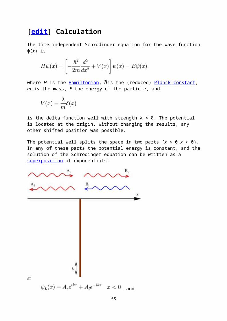
[edit] ApplicationsThe nonlinear nature of ferroelectric materials can be used to make capacitors with tunable capacitance. Typically, a ferroelectric capacitor simply consists of a pair of electrodes sandwiching a layer of ferroelectric material. The permittivity of ferroelectrics is not only tunable but commonly also very high in absolute value, especially when close to the phase transition temperature. This fact makes ferroelectric capacitors small in size compared to dielectric (non-tunable) capacitors of similar capacitance.
The spontaneous polarization of ferroelectric materials implies a hysteresis effect which can be used as a memory function. Indeed, ferroelectric capacitors are used to make ferroelectric RAM [3] for computers and RFID cards. These applications are usually based on thin films of ferroelectric materials as this allows the high coercive field required to switch the polarization to be achieved with a moderate voltage, though a side effect of this is that a great deal of attention needs to be paid to the interfaces, electrodes and sample quality for devices to work reliably[4].
All ferroelectrics are required by symmetry considerations to be also piezoelectric and pyroelectric. The combined properties of memory, piezoelectricity, and pyroelectricity make ferroelectric capacitors very useful, e.g. for sensor applications. Ferroelectric capacitors are used in medical ultrasound machines (the capacitors generate and then listen for the ultrasound ping used to image the internal organs of a body), high quality infrared cameras (the infrared image is projected onto a two dimensional array of ferroelectric capacitors capable of detecting temperature differences as small as millionths of a degree Celsius), fire sensors, sonar, vibration sensors, and even fuel injectors on diesel engines. As well, the electro-optic modulators that form the backbone of the Internet are made with ferroelectric materials.
One new idea of recent interest is the ferroelectric tunnel junction (FTJ) in which a contact made up by nanometer-thick ferroelectric film placed between metal electrodes. The thickness of the ferroelectric layer is thin enough to allow tunneling of electrons. The piezoelectric and interface effects as well as the depolarization field may lead to a giant electroresistance (GER) switching effect.
Another hot topic is Multiferroics, where researchers are looking for ways to couple magnetic and ferroelectric ordering within a material or heterostructure; there are several recent reviews on this topic [5].
[edit] MaterialsThe internal electric dipoles of a ferroelectric material are physically tied to the material lattice so anything that changes the physical lattice will change the strength of the dipoles and cause a current to flow into or out of the capacitor even without the presence of an external voltage across the capacitor. Two stimuli that will change the lattice dimensions of a material are force and temperature. The generation of a current in response to the application of a force to a capacitor is called piezoelectricity. The generation of current in response to a change in temperature is called pyroelectricity.
55
Ferroelectric phase transitons are often characterized as either displacive and order-disorder, though often phase transitions will have behaviour that contains elements of both behaviours. In barium titanate, a typical ferroelectric of the displacive type, the transition can be understood in terms of a polarization catastrophe, in which, if an ion is displaced from equilibrium slightly, the force from the local electric fields due to the ions in the crystal increases faster than the elastic-restoring forces. This leads to an asymmetrical shift in the equilibrium ion positions and hence to a permanent dipole moment. The ionic displacement in barium titanate concerns the relative position of the titanium ion within the oxygen octahedral cage.In lead titanate,another key ferroelectric material, although the structure is rather similar to barium titanate the driving force for ferroelectricity is more complex with interactions between the lead and oxygen ions also playing an important role. In an order-disorder ferroelectric, there is a dipole moment in each unit cell, but at high temperatures they are pointing in random directions. Upon lowering the temperature and going through the phase transition, the dipoles order, all pointing in the same direction within a domain.
An important ferroelectric material for applications is lead zirconate titanate(PZT), which is part of the solid solution formed between ferroelectric lead titanate and anti-ferroelectric lead zirconate. Different compositions are used for different applications, for memory application PZT closer in composition to lead titanate is preferred, whereas piezoelectric applications make use of the diverging piezoelectric coefficients associated with the morphotropic phase boundary that is found close to 50/50 composition.
In 1979 Swedish Sven Torbjörn Lagerwall discovered ferroelectric liquid crystals in collaboration with Noel Clark. The technology allows the building of flat-screen monitors. Mass production began in 1994 by Canon, who bought the licence.
Ferroelectric crystals often show several transition temperatures and domain structure hysteresis, much as do ferromagnetic crystals. The nature of the phase transition in some ferroelectric crystals is still not well understood.
The ferroelectric effect also finds use in liquid crystal physics by incorporation of a chiral dopant into an achiral smectic C matrix. These liquid crystals exhibit the Clark-Lagerwall effect [6] which effects a change in one bistable state to another upon switching of electric field direction.
[edit] See also Stabilizing ferroelectric materials FeRAM
[edit] Physics
Paraelectricity Piezoelectricity
Pyroelectricity
Condensed matter physics
Spintronics
56
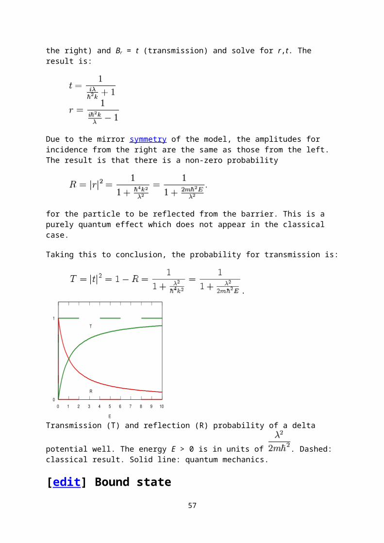
Ceramics
[edit] Lists
Examples of electrical phenomena List of physics topics
List of electronics topics
[edit] References1. ̂ M. Lines,A. Glass, Principles and applications of ferroelectrics and related materials
(Clarendon Press, Oxford, 1979)2. ̂ J. Valasek, Piezoelectric and allied phenomena in Rochelle Salt Phys. Rev. 15, 537
(1920),"Phys. Rev."17, 475 (1921)
3. ̂ J.F. Scott, Ferroelectric Memories, Springer (2000)
4. ̂ M. Dawber, K.M. Rabe, J.F. Scott, Physics of thin-film ferroelectric oxides Rev. Mod. Phys 77 1083 (2005).
5. ̂ R. Ramesh,N.A Spaldin, Nature Materials 6 21 (2007),W. Eerenstein,N.D. Mathur,J.F. Scott, Nature 442 759 (2006),N.A. Spaldin, M. Fiebig, Science 309 5391 (2005),M. Fiebig, J Phys. D , 38 R123 (2005)
6. ̂ Noel A. Clark, Sven Torbjörn Lagerwall: Submicrosecond Bistable Electro-Optic Switching in Liquid Crystals, Appl. Phys. Lett. 36, 899 (1980)
[edit] External links A useful starter on ferroelectrics A ferroelectrics research group at Stony Brook University
Retrieved from "http://en.wikipedia.org/wiki/Ferroelectricity"Categories: Condensed matter physics | Electrical phenomena
Quantum Tunneling CompositeFrom Wikipedia, the free encyclopedia
Jump to: navigation, search
Quantum Tunnelling Composites (or QTCs) are composite materials of metals and non-conducting elastomeric binder, used as pressure sensors. As the name implies, they operate using quantum tunnelling: without pressure, the conductive elements are too far apart to conduct electricity; when pressure is applied, they move closer and electrons can tunnel through the insulator. The effect is far more pronounced than would be expected from classical (non-quantum) effects alone, as classical electrical resistance is linear (proportional
57
to distance), while quantum tunnelling is exponential with decreasing distance, allowing the resistance to change by a factor of up to 1012 between pressured and unpressured states.
[edit] ApplicationsQTC has been implemented within clothing to make “smart”, touchable membrane control panels to control electronic devices within the clothing, e.g. mp3 players or mobile phones. This allows equipment to be operated without removing clothing layers or opening fastenings and makes standard equipment usable in extreme weather or environmental conditions such as Arctic/Antarctic exploration or spacesuits. However, eventually, due to the low cost of QTC, this technology will become available to the general user.
[edit] DiscoveryQTCs were discovered in 1996 and PeraTech Ltd was established to investigate them further.
[edit] External links PeraTech Ltd website
This electronics-related article is a stub. You can help Wikipedia by expanding it.Retrieved from "http://en.wikipedia.org/wiki/Quantum_Tunneling_Composite"Categories: Electrical components | Quantum electronics | Electronics stubs
58


![96FBGA with Lead-Free & Halogen-Free · DDR3 SDRAM Addressing ... [ Table 47 ] DDR3-800 Speed Bins [ Table 48 ] DR3-1066 Speed Bins Parameter Symbol 1Gb 2Gb 4Gb 8Gb Units NOTE](https://img.pdfslide.us/doc/110x75/5ad5dbf67f8b9a5c638d9a8c/96fbga-with-lead-free-halogen-free-sdram-addressing-table-47-ddr3-800-speed.jpg)