Embed Size (px)
Citation preview
WP2 Review MeetingMilan, October 05, 2011
MODERN ENIAC WP2 Meeting(WP2-T2.4)
WP2 and Tasks review
Milano Agrate, 2011 Oct. 05
Meeting hosted by Micron
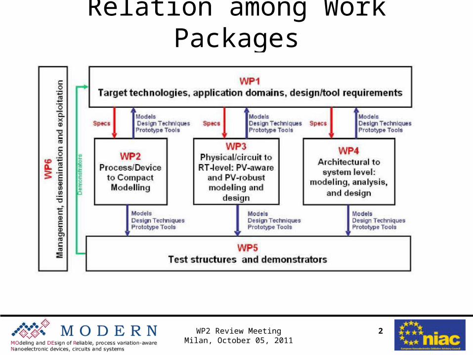
Relation among Work Packages
2WP2 Review MeetingMilan, October 05, 2011

T2.4 Task (1/2)• Task T2.4: Correlation between PV and reliability, reliability modeling• The impact of process variability on existing device reliability degradation models will be clarified.
Aging measure-ments will be performed on test structures: Device degradation mechanisms will be identified based on silicon, their effect on PV parameters will be characterized and modeled to allow for a better description of aging during operation.
• Partners: AMS, IMEP, UNET, TUW, UNCA, UNGL• UNGL will develop methodologies for the simulation of the statistical impact of NBTI and hot
carrier degradation on the MOSFET characteristics in concert with the statistical variability sources described in T2.2 and its capture in statistical compact models. UNCA will perform aging measurements on nano-MOSFET devices focusing on the three main reliability mechanisms: hot-carrier injection, bias-temperature instability and time-dependent dielectric breakdown. The impact of process variation (e.g. line edge roughness, random dopant distribution, non-homogenity of the gate dielectric) on the device reliability will be investigated and potential solutions will be proposed. Aging models will be developed to predict device lifetime dependence on the statistical fluctuations of geometrical and technological parameters of nano-MOSFET. Model parameters will be calibrated with the hardware results of aging measurements. UNET will work on methodologies to design reliability experiments that allow characterizing the impact of PV on test structures, single cells or simple arrays, on 45nm & 32nm planar CMOS, and on Non-Volatile Memories. It will include the development of compact models including aging effects. AMS will execute lifetime measurements necessary for model development and the usage in SPICE simulators in 0.13um, 0.18um and 0.35um CMOS and HV technologies. The objective is to develop silicon based models for PV and reliability correlation. Lifetime measurements will be performed on appropriate test structures. Based on that data set, PV-aware parameter degradation models for NBTI and HCI effects will be developed at TUW. Since in particular degradation caused by NBTI is known to recover quickly once the stress is removed, emphasis will be put on a proper description of the dynamical properties of the degradation.
3WP2 Review MeetingMilan, October 05, 2011
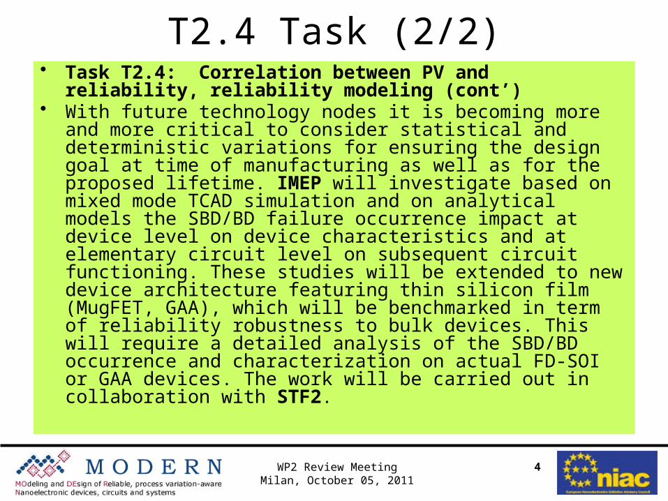
T2.4 Task (2/2)• Task T2.4: Correlation between PV and reliability, reliability
modeling (cont’)• With future technology nodes it is becoming more and more critical
to consider statistical and deterministic variations for ensuring the design goal at time of manufacturing as well as for the proposed lifetime. IMEP will investigate based on mixed mode TCAD simulation and on analytical models the SBD/BD failure occurrence impact at device level on device characteristics and at elementary circuit level on subsequent circuit functioning. These studies will be extended to new device architecture featuring thin silicon film (MugFET, GAA), which will be benchmarked in term of reliability robustness to bulk devices. This will require a detailed analysis of the SBD/BD occurrence and characterization on actual FD-SOI or GAA devices. The work will be carried out in collaboration with STF2.
4WP2 Review MeetingMilan, October 05, 2011
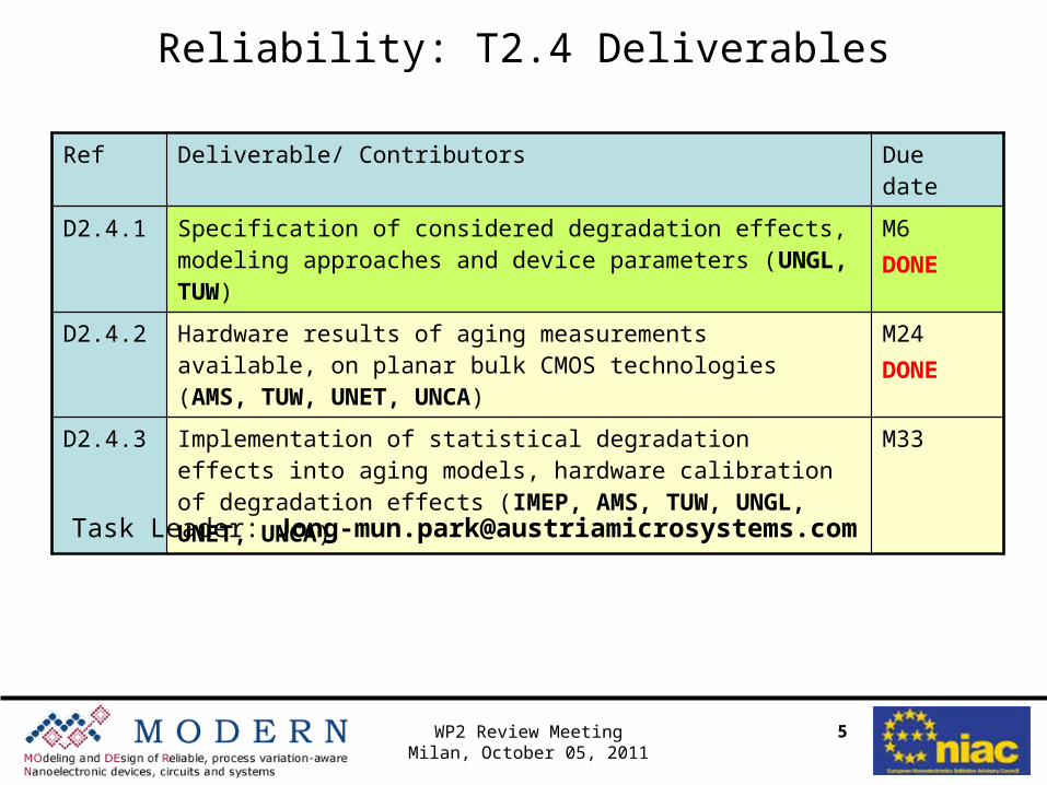
Reliability: T2.4 Deliverables
Ref Deliverable/ Contributors Due date
D2.4.1 Specification of considered degradation effects, modeling approaches and device parameters (UNGL, TUW)
M6DONE
D2.4.2 Hardware results of aging measurements available, on planar bulk CMOS technologies (AMS, TUW, UNET, UNCA)
M24DONE
D2.4.3 Implementation of statistical degradation effects into aging models, hardware calibration of degradation effects (IMEP, AMS, TUW, UNGL, UNET, UNCA)
M33
Task Leader: [email protected]
5WP2 Review MeetingMilan, October 05, 2011
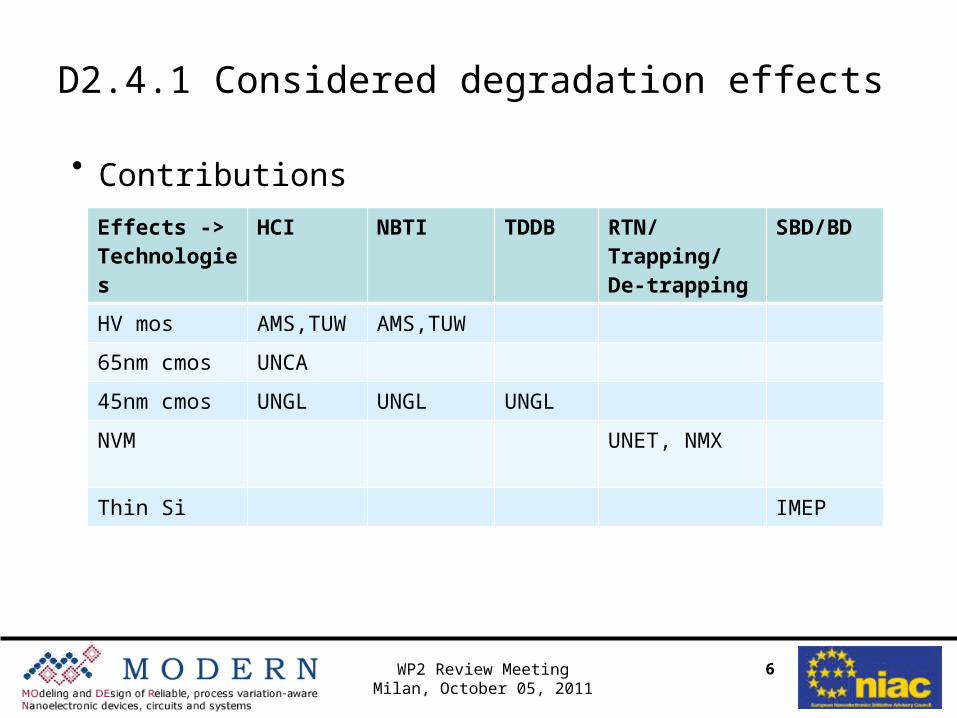
D2.4.1 Considered degradation effects
• Contributions Effects ->Technologies
HCI NBTI TDDB RTN/Trapping/De-trapping
SBD/BD
HV mos AMS,TUW AMS,TUW
65nm cmos UNCA
45nm cmos UNGL UNGL UNGL
NVM UNET, NMX
Thin Si IMEP
6WP2 Review MeetingMilan, October 05, 2011
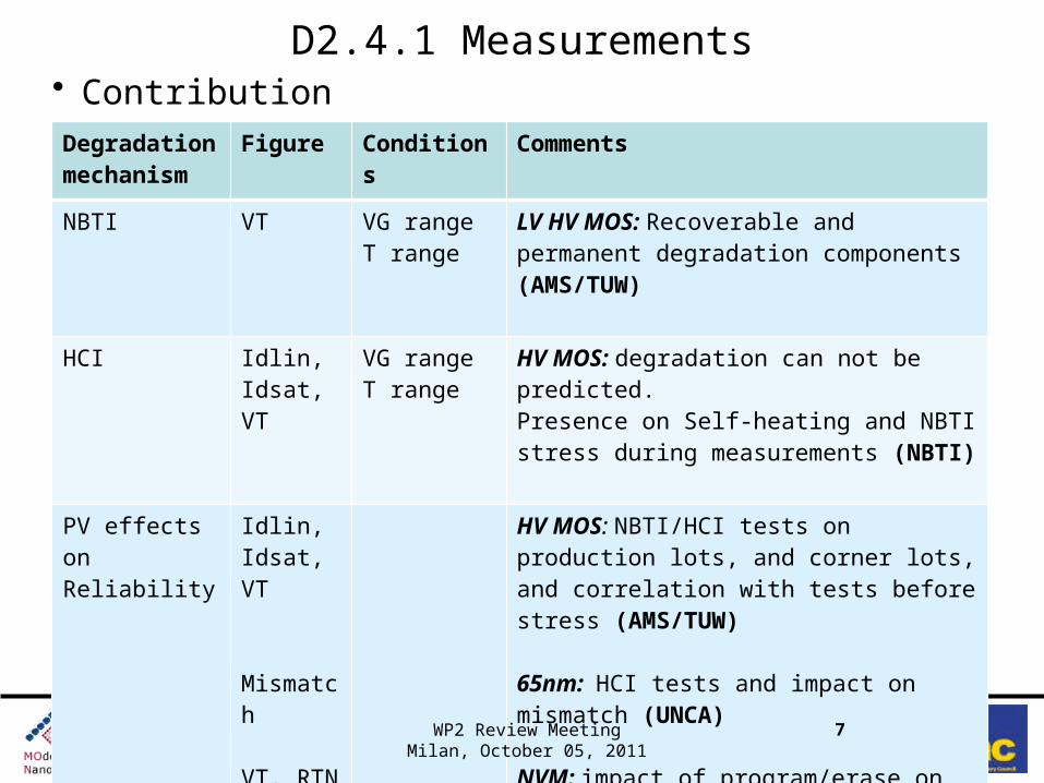
D2.4.1 Measurements• Contributions Degradation mechanism
Figure Conditions Comments
NBTI VT VG rangeT range
LV HV MOS: Recoverable and permanent degradation components (AMS/TUW)
HCI Idlin, Idsat, VT
VG rangeT range
HV MOS: degradation can not be predicted.Presence on Self-heating and NBTI stress during measurements (NBTI)
PV effects on Reliability
Idlin, Idsat, VT
Mismatch
VT, RTN
HV MOS: NBTI/HCI tests on production lots, and corner lots, and correlation with tests before stress (AMS/TUW)
65nm: HCI tests and impact on mismatch (UNCA)
NVM: impact of program/erase on Trapped Interface/Oxide charges (IUNET)
7WP2 Review MeetingMilan, October 05, 2011
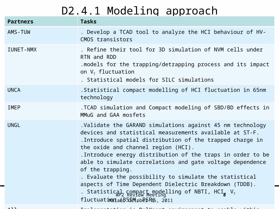
D2.4.1 Modeling approachPartners Tasks
AMS-TUW . Develop a TCAD tool to analyze the HCI behaviour of HV-CMOS transistors
IUNET-NMX . Refine their tool for 3D simulation of NVM cells under RTN and RDD.models for the trapping/detrapping process and its impact on VT fluctuation. Statistical models for SILC simulations
UNCA .Statistical compact modelling of HCI fluctuation in 65nm technology
IMEP .TCAD simulation and Compact modeling of SBD/BD effects in MMuG and GAA mosfets
UNGL .Validate the GARAND simulations against 45 nm technology devices and statistical measurements available at ST-F..Introduce spatial distribution of the trapped charge in the oxide and channel region (HCI)..Introduce energy distribution of the traps in order to be able to simulate correlations and gate voltage dependence of the trapping.. Evaluate the possibility to simulate the statistical aspects of Time Dependent Dielectric Breakdown (TDDB).. Statistical compact modelling of NBTI, HCI, VT fluctuation (BSIM, PSP)
All Implementation in RelXpert environment to enable within Design flow:.Fresh simulation.Calculation of the aging using some analytical expression.Degradation of the SPICE parameters and updating the netlist.Re-simulation with degraded netlist
8WP2 Review MeetingMilan, October 05, 2011
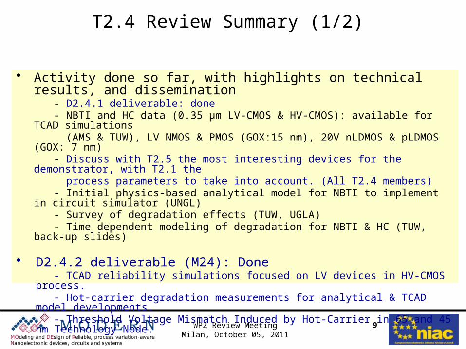
T2.4 Review Summary (1/2)
• Activity done so far, with highlights on technical results, and dissemination
- D2.4.1 deliverable: done - NBTI and HC data (0.35 µm LV-CMOS & HV-CMOS): available for TCAD simulations (AMS & TUW), LV NMOS & PMOS (GOX:15 nm), 20V nLDMOS & pLDMOS (GOX: 7 nm) - Discuss with T2.5 the most interesting devices for the demonstrator, with T2.1 the process parameters to take into account. (All T2.4 members) - Initial physics-based analytical model for NBTI to implement in circuit simulator (UNGL) - Survey of degradation effects (TUW, UGLA) - Time dependent modeling of degradation for NBTI & HC (TUW, back-up slides)
• D2.4.2 deliverable (M24): Done - TCAD reliability simulations focused on LV devices in HV-CMOS process. - Hot-carrier degradation measurements for analytical & TCAD model developments. - Threshold Voltage Mismatch Induced by Hot-Carrier in 65 and 45 nm Technology Node.
9WP2 Review MeetingMilan, October 05, 2011
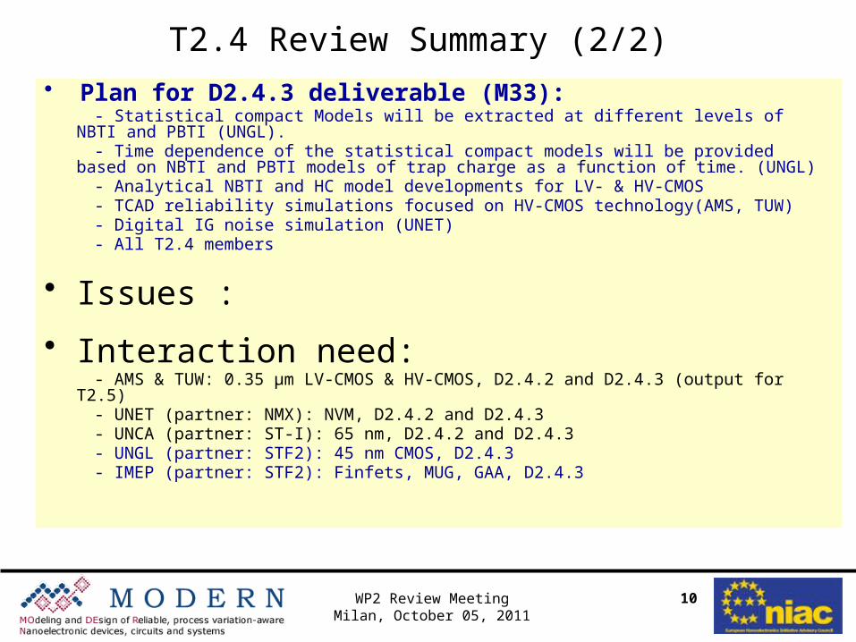
T2.4 Review Summary (2/2) • Plan for D2.4.3 deliverable (M33): - Statistical compact Models will be extracted at different levels of NBTI and PBTI (UNGL). - Time dependence of the statistical compact models will be provided based on NBTI and PBTI models
of trap charge as a function of time. (UNGL) - Analytical NBTI and HC model developments for LV- & HV-CMOS - TCAD reliability simulations focused on HV-CMOS technology(AMS, TUW) - Digital IG noise simulation (UNET) - All T2.4 members
• Issues :
• Interaction need: - AMS & TUW: 0.35 µm LV-CMOS & HV-CMOS, D2.4.2 and D2.4.3 (output for T2.5) - UNET (partner: NMX): NVM, D2.4.2 and D2.4.3 - UNCA (partner: ST-I): 65 nm, D2.4.2 and D2.4.3 - UNGL (partner: STF2): 45 nm CMOS, D2.4.3 - IMEP (partner: STF2): Finfets, MUG, GAA, D2.4.3
10WP2 Review MeetingMilan, October 05, 2011
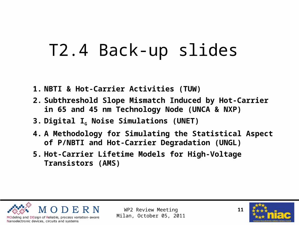
T2.4 Back-up slides
11
1. NBTI & Hot-Carrier Activities (TUW)
2. Subthreshold Slope Mismatch Induced by Hot-Carrier in 65 and 45 nm Technology Node (UNCA & NXP)
3. Digital IG Noise Simulations (UNET)
4. A Methodology for Simulating the Statistical Aspect of P/NBTI and Hot-Carrier Degradation (UNGL)
5. Hot-Carrier Lifetime Models for High-Voltage Transistors (AMS)
WP2 Review MeetingMilan, October 05, 2011
12
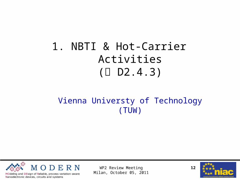
1. NBTI & Hot-Carrier Activities( D2.4.3)
Vienna Universty of Technology (TUW)
WP2 Review MeetingMilan, October 05, 2011
13WP2 Review MeetingMilan, October 05, 2011
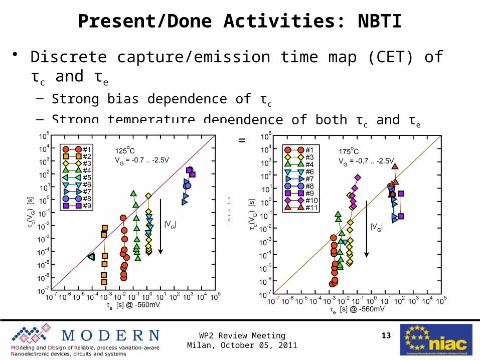
Present/Done Activities: NBTI
• Discrete capture/emission time map (CET) of τc and τe
– Strong bias dependence of τc
– Strong temperature dependence of both τc and τe
– Note: τc = τc(VH) and τc = τc(VL)
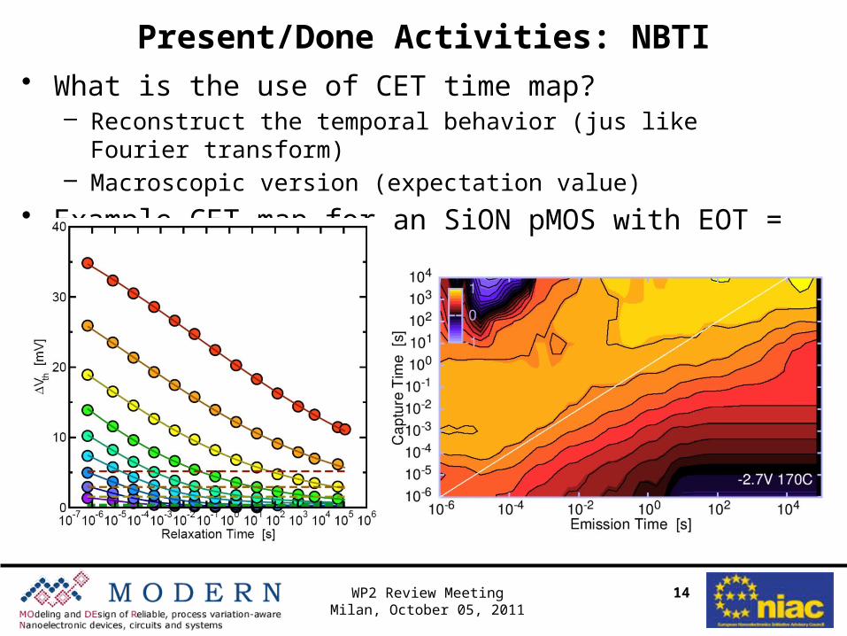
14WP2 Review MeetingMilan, October 05, 2011
Present/Done Activities: NBTI• What is the use of CET time map?
– Reconstruct the temporal behavior (jus like Fourier transform)– Macroscopic version (expectation value)
• Example CET map for an SiON pMOS with EOT = 2.2 nm
15WP2 Review MeetingMilan, October 05, 2011
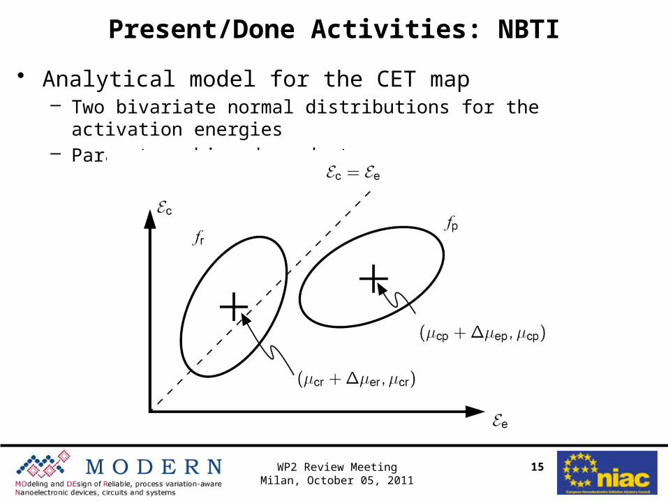
Present/Done Activities: NBTI
• Analytical model for the CET map– Two bivariate normal distributions for the activation energies– Parameters bias-dependent
16WP2 Review MeetingMilan, October 05, 2011
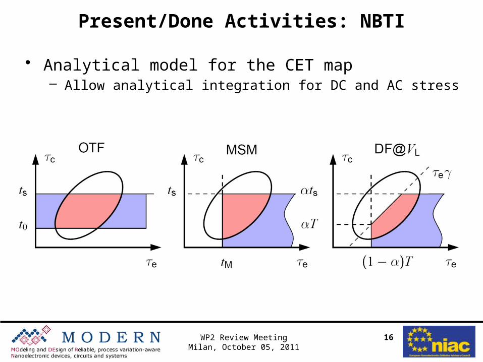
Present/Done Activities: NBTI
• Analytical model for the CET map – Allow analytical integration for DC and AC stress
17WP2 Review MeetingMilan, October 05, 2011
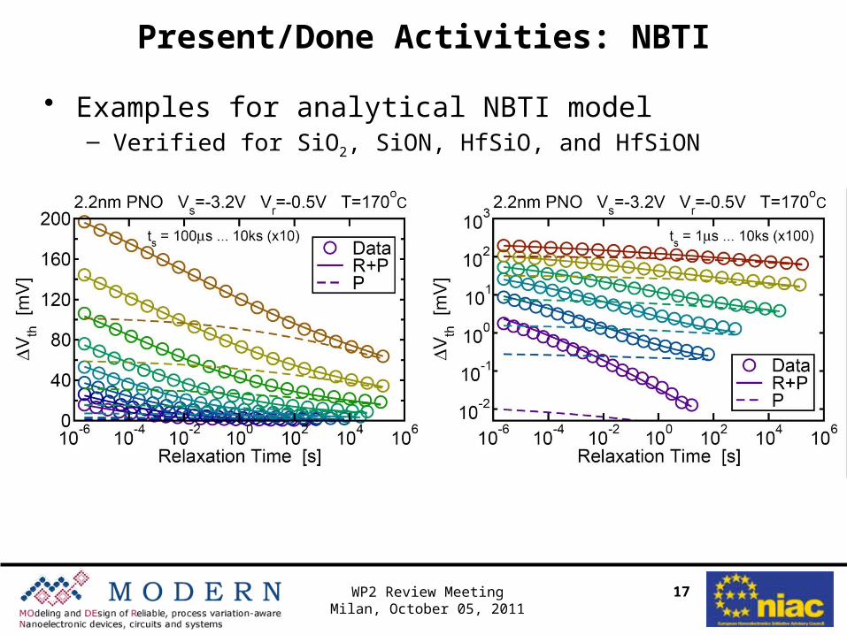
Present/Done Activities: NBTI
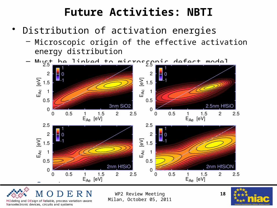
• Examples for analytical NBTI model – Verified for SiO2, SiON, HfSiO, and HfSiON
18WP2 Review MeetingMilan, October 05, 2011
Future Activities: NBTI
• Distribution of activation energies– Microscopic origin of the effective activation energy distribution – Must be linked to microscopic defect model
19WP2 Review MeetingMilan, October 05, 2011
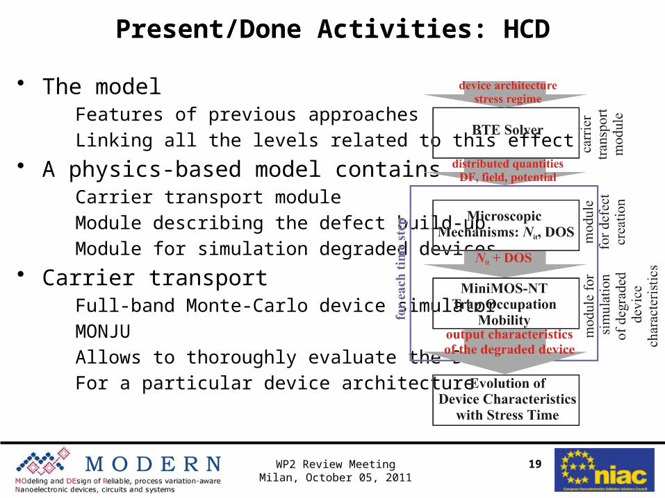
Present/Done Activities: HCD
• The model Features of previous approaches
Linking all the levels related to this effect
• A physics-based model containsCarrier transport module
Module describing the defect build-up
Module for simulation degraded devices
• Carrier transport Full-band Monte-Carlo device simulator
MONJU
Allows to thoroughly evaluate the DF
For a particular device architecture
20WP2 Review MeetingMilan, October 05, 2011
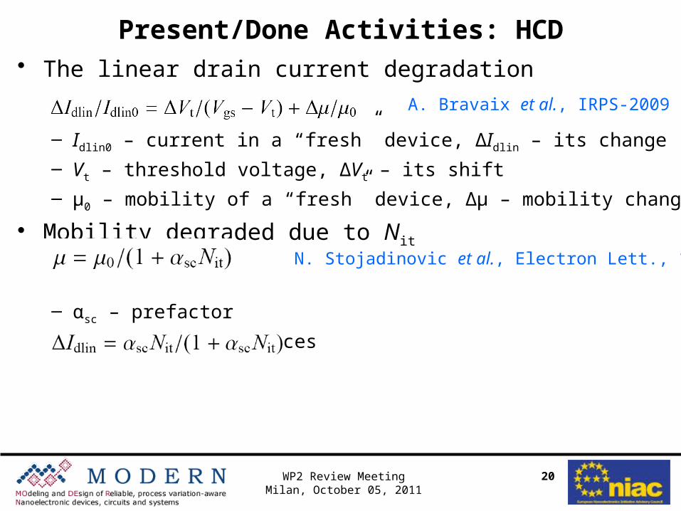
Present/Done Activities: HCD• The linear drain current degradation
– Idlin0 – current in a “fresh” device, ΔIdlin – its change
– Vt – threshold voltage, ΔVt – its shift
– μ0 – mobility of a “fresh” device, Δμ – mobility change
• Mobility degraded due to Nit
– αsc – prefactor
– ΔVt ≈ 0 in our devices
A. Bravaix et al., IRPS-2009
N. Stojadinovic et al., Electron Lett., 1995
21WP2 Review MeetingMilan, October 05, 2011
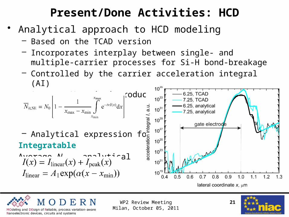
Present/Done Activities: HCD• Analytical approach to HCD modeling
– Based on the TCAD version – Incorporates interplay between single- and multiple-carrier
processes for Si-H bond-breakage– Controlled by the carrier acceleration integral (AI)– Average Nit,SE is introduced
– Analytical expression for I(x)
Integratable
Average Nit → analytical
22WP2 Review MeetingMilan, October 05, 2011
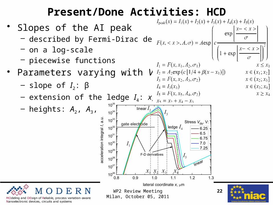
Present/Done Activities: HCD• Slopes of the AI peak
– described by Fermi-Dirac derivatives– on a log-scale– piecewise functions
• Parameters varying with Vds:– slope of I2: β
– extension of the ledge I4: x4-x3
– heights: A2, A3, A4
23WP2 Review MeetingMilan, October 05, 2011
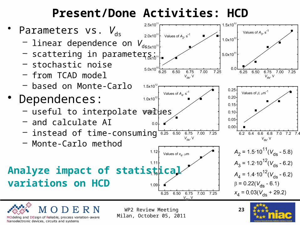
Present/Done Activities: HCD• Parameters vs. Vds
– linear dependence on Vds
– scattering in parameters:– stochastic noise– from TCAD model– based on Monte-Carlo
• Dependences:– useful to interpolate values– and calculate AI– instead of time-consuming– Monte-Carlo method
Analyze impact of statisticalvariations on HCD
24WP2 Review MeetingMilan, October 05, 2011
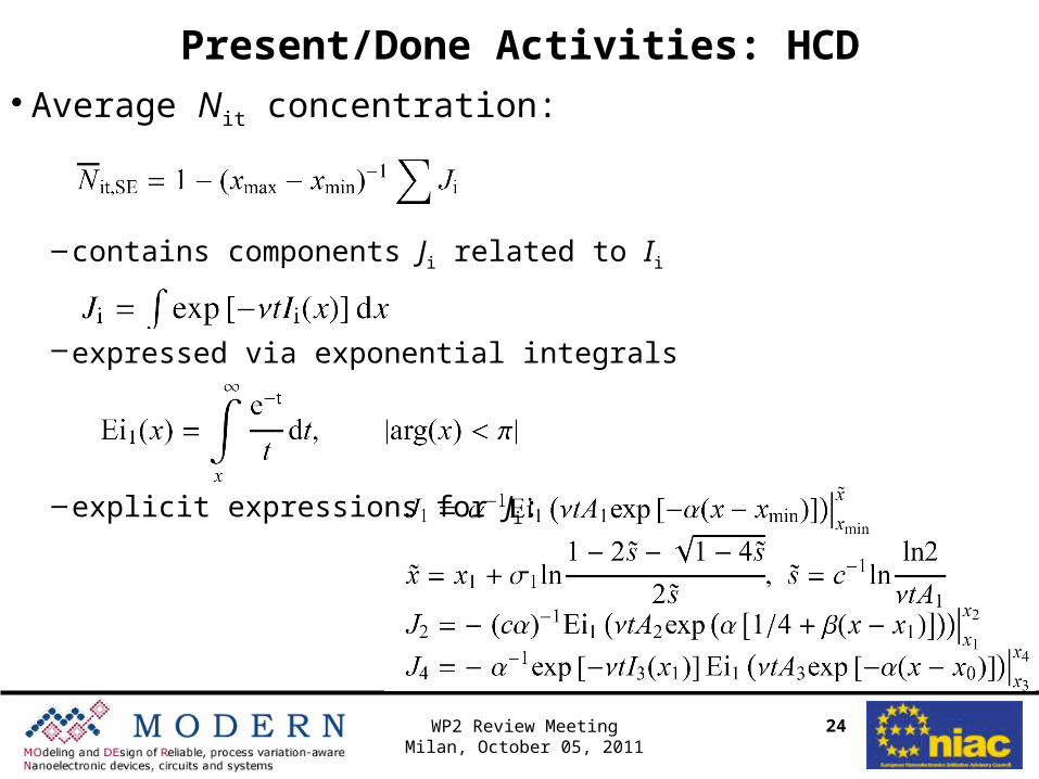
Present/Done Activities: HCD• Average Nit concentration:
–contains components Ji related to Ii
–expressed via exponential integrals
–explicit expressions for Ji:
25WP2 Review MeetingMilan, October 05, 2011
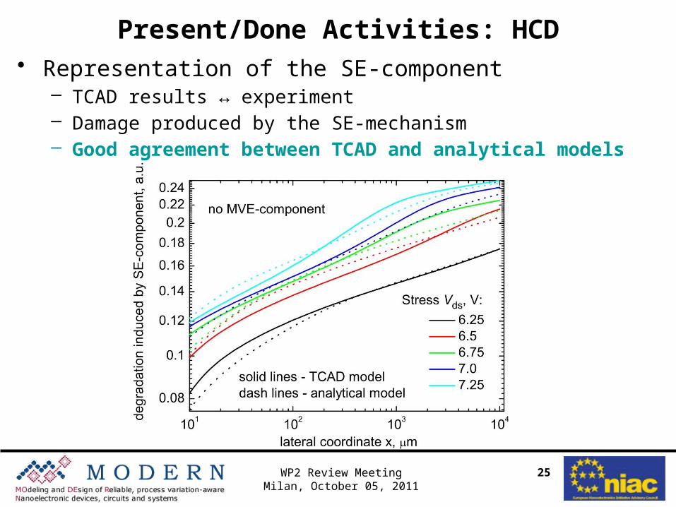
Present/Done Activities: HCD• Representation of the SE-component
– TCAD results ↔ experiment– Damage produced by the SE-mechanism– Good agreement between TCAD and analytical models
26WP2 Review MeetingMilan, October 05, 2011
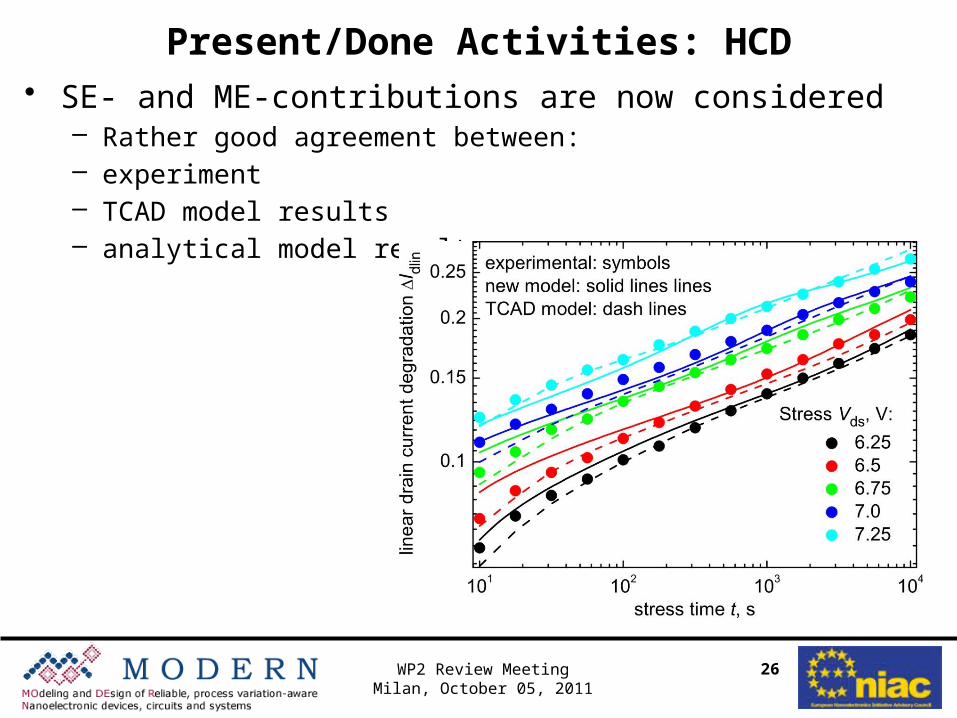
Present/Done Activities: HCD• SE- and ME-contributions are now considered
– Rather good agreement between:– experiment– TCAD model results– analytical model results
27WP2 Review MeetingMilan, October 05, 2011
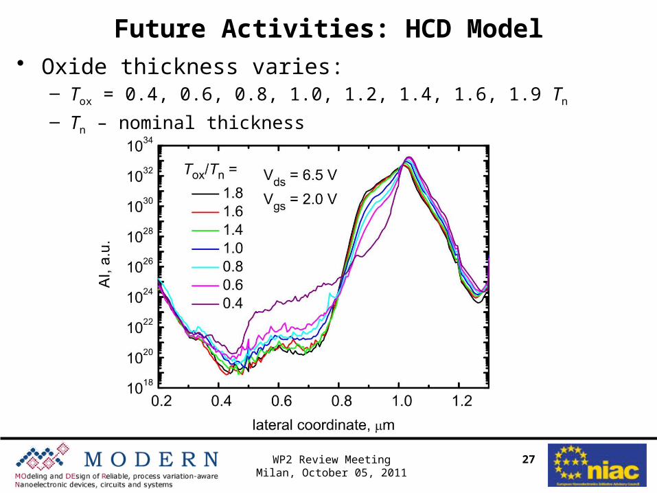
Future Activities: HCD Model• Oxide thickness varies:
– Tox = 0.4, 0.6, 0.8, 1.0, 1.2, 1.4, 1.6, 1.9 Tn
– Tn – nominal thickness
2. Subthreshold Slope Mismatch Induced by Hot-Carrier in 65 and 45 nm Technology Node
(Ref.: D2.4.2)
Universty of Calabria (UNCA)in collaboration with NXP
28WP2 Review MeetingMilan, October 05, 2011
29
PURPOSE
To characterize and to model theHC-induced subthreshold slope variability
in 65 nm and 45 nm technology node
WP2 Review MeetingMilan, October 05, 2011
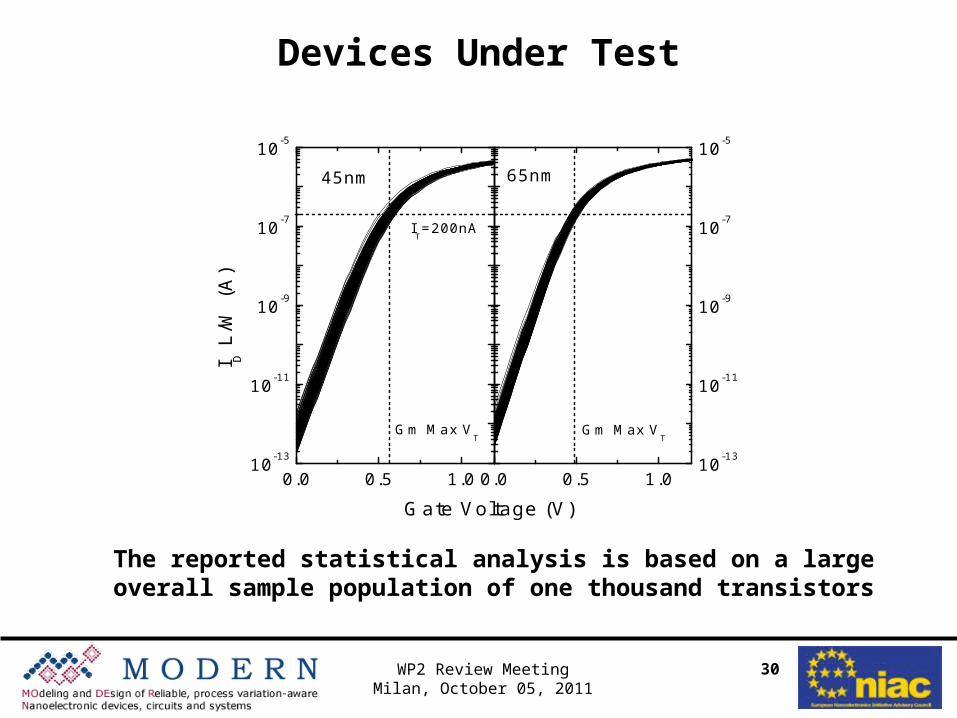
30WP2 Review MeetingMilan, October 05, 2011
Devices Under Test
0.0 0.5 1.010-13
10-11
10-9
10-7
10-5
IT=200nA
Gate Voltage (V)
Gm Max VT
65nm
0.0 0.5 1.010-13
10-11
10-9
10-7
10-5
I D L
/W (
A)
45nm
Gm Max VT
The reported statistical analysis is based on a large overall sample population of one thousand transistors
31WP2 Review MeetingMilan, October 05, 2011
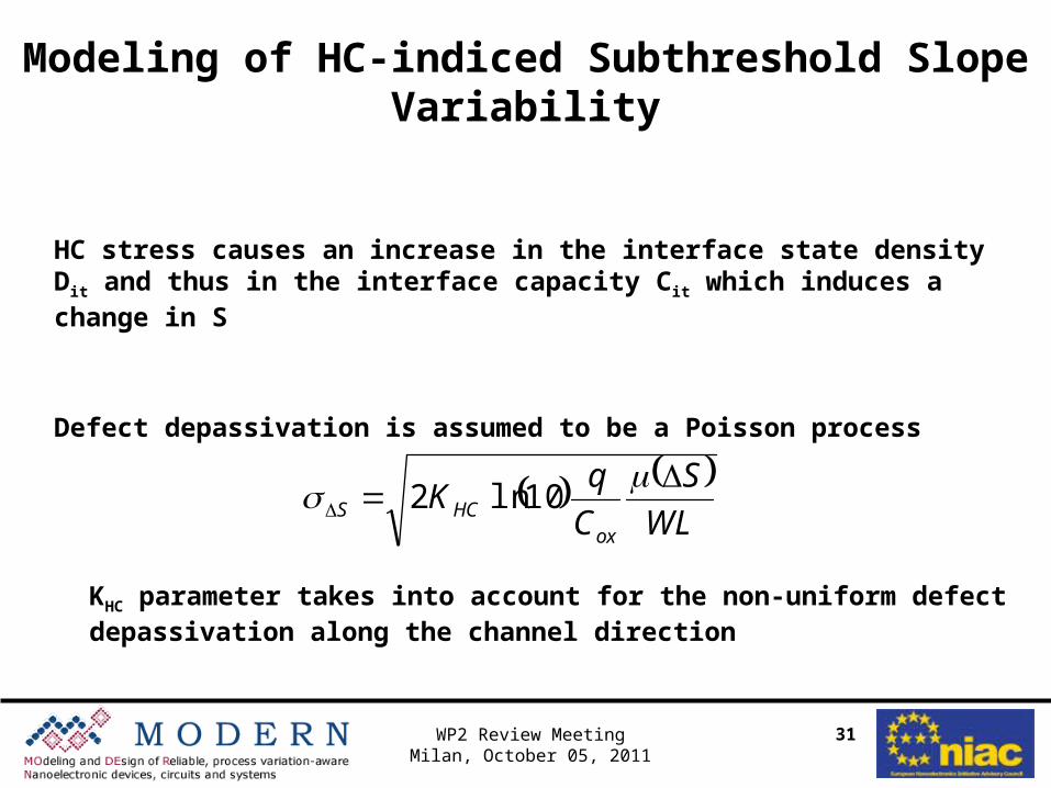
Modeling of HC-indiced Subthreshold Slope Variability
HC stress causes an increase in the interface state density Dit and thus in the interface capacity Cit which induces a change in S
Defect depassivation is assumed to be a Poisson process
KHC parameter takes into account for the non-uniform defect depassivation along the channel direction
WL
S
C
qK
oxHCS
10ln2
32WP2 Review MeetingMilan, October 05, 2011
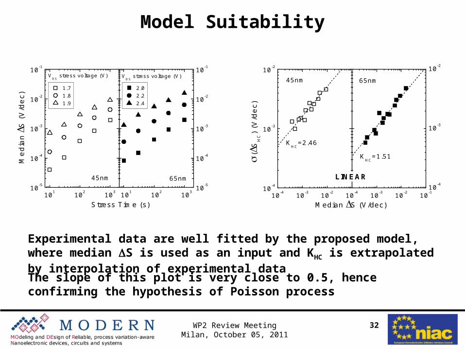
Model Suitability
Experimental data are well fitted by the proposed model, where median DS is used as an input and KHC is extrapolated by interpolation of experimental data
101 102 10310-5
10-4
10-3
10-2
10-1
1.71.81.9
45nm
Media
n
S (
V/d
ec)
Stress Time (s)
VDS
stress voltage (V)
101 102 10310-5
10-4
10-3
10-2
10-1
VDS
stress voltage (V)
2.02.22.4
65nm
10-4 10-3 10-210-4
10-3
10-2
(
SH
C)
(V/d
ec)
Median S (V/dec)
45nm
KHC
=2.46
10-4 10-3 10-2 10-110-4
10-3
10-2
LINEAR
KHC
=1.51
65nm
The slope of this plot is very close to 0.5, hence confirming the hypothesis of Poisson process
33WP2 Review MeetingMilan, October 05, 2011
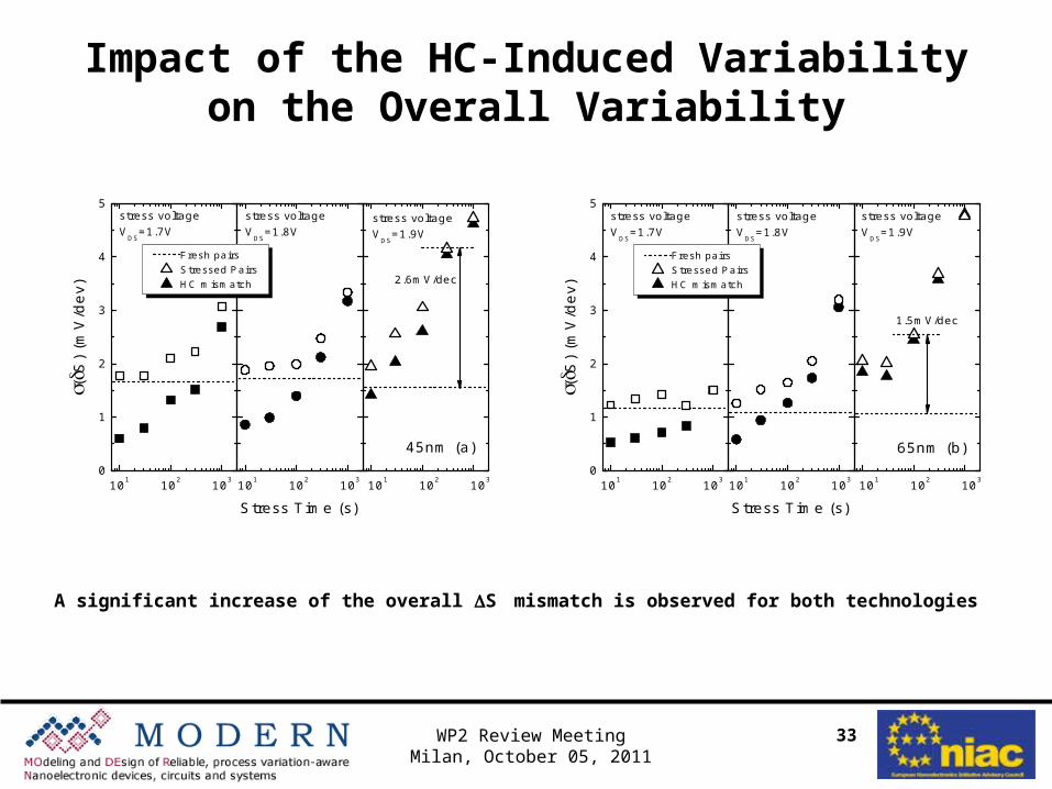
Impact of the HC-Induced Variability on the Overall Variability
A significant increase of the overall DS mismatch is observed for both technologies
101 102 1030
1
2
3
4
5stress voltageV
DS=1.7V
(S
) (m
V/d
ev)
Stress Time (s)101 102 103
stress voltageV
DS=1.8V
101 102 103
2.6mV/dec
Fresh pairsStressed PairsHC mismatch
45nm (a)
stress voltageV
DS=1.9V
101 102 1030
1
2
3
4
5stress voltageV
DS=1.7V
(S
) (m
V/d
ev)
Stress Time (s)101 102 103
stress voltageV
DS=1.8V
101 102 103
1.5mV/dec
Fresh pairsStressed PairsHC mismatch
65nm (b)
stress voltageV
DS=1.9V
34WP2 Review MeetingMilan, October 05, 2011
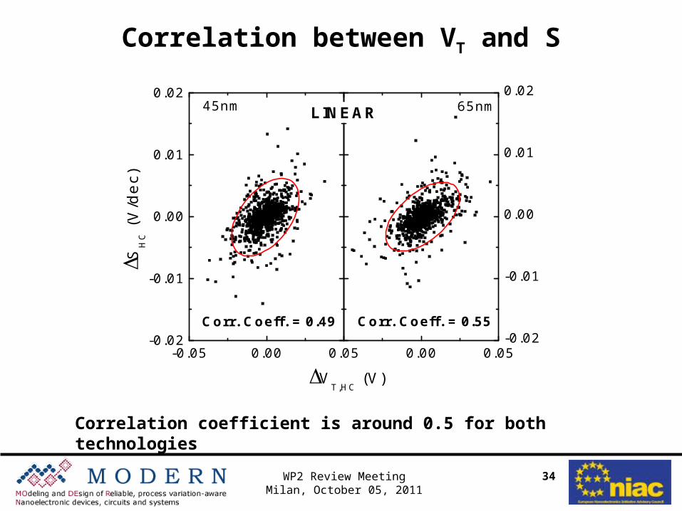
Correlation coefficient is around 0.5 for both technologies
-0.05 0.00 0.05-0.02
-0.01
0.00
0.01
0.02
Corr. Coeff. = 0.49
SH
C (
V/d
ec)
VT,HC
(V)
45nm
0.00 0.05-0.02
-0.01
0.00
0.01
0.02
LINEAR
Corr. Coeff. = 0.55
65nm
Correlation between VT and S
3. Digital IG noise simulations
( D2.4.3)
Consorzio Nazionale Interuniversitario per la Nanoelettronica
(UNET)
35WP2 Review MeetingMilan, October 05, 2011
36WP2 Review MeetingMilan, October 05, 2011
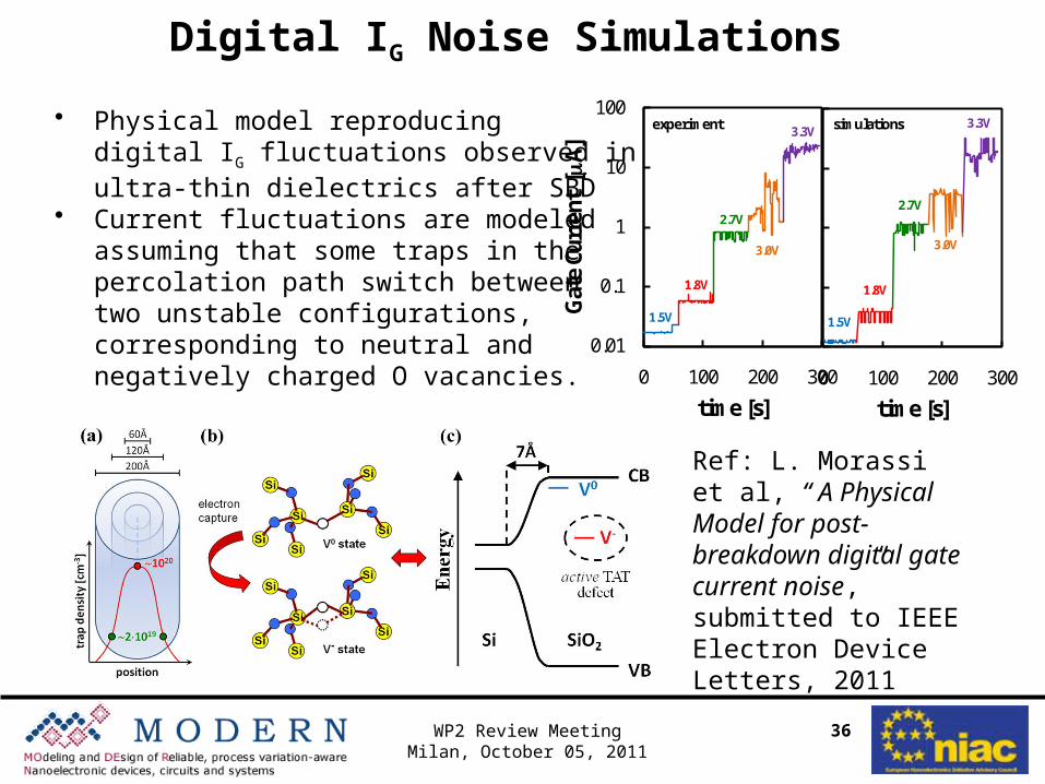
• Physical model reproducingdigital IG fluctuations observed inultra-thin dielectrics after SBD
• Current fluctuations are modeledassuming that some traps in thepercolation path switch betweentwo unstable configurations,corresponding to neutral andnegatively charged O vacancies.
Digital IG Noise Simulations
0.01
0.1
1
10
100
0 100 200 300
Gat
e Cu
rren
t [
A]
time [s]
experiment
1.5V
1.8V
2.7V
3.0V
3.3V
1.5V
1.8V
2.7V
3.0V
3.3V
0 100 200 300
time [s]
simulations
Ref: L. Morassi et al, “ A Physical Model for post-breakdown digital gate current noise,” submitted to IEEE Electron Device Letters, 2011
4. A Methodology for Simulating the Statistical Aspect of P/NBTI and Hot-Carrier Degradation
( D2.4.3)
The University of Glasgow (UNGL)
37WP2 Review MeetingMilan, October 05, 2011
38WP2 Review MeetingMilan, October 05, 2011
Purpose
• We developed a methodology for simulating the statistical aspect of P/NBTI and hot carrier degradation in 32nm RVT N/PMOS.
• Random trapped charges due to P/NBTI stress are assigned to interface degradation.
• The threshold-voltage shift is observed and its variations are analyzed.
39WP2 Review MeetingMilan, October 05, 2011
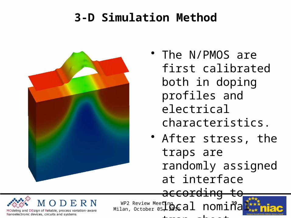
3-D Simulation Method
• The N/PMOS are first calibrated both in doping profiles and electrical characteristics.
• After stress, the traps are randomly assigned at interface according to local nominal trap sheet density.
40WP2 Review MeetingMilan, October 05, 2011
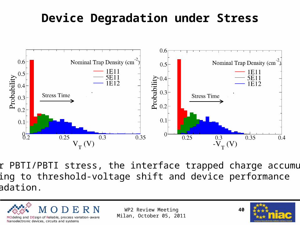
Device Degradation under Stress
Under PBTI/PBTI stress, the interface trapped charge accumulates, leading to threshold-voltage shift and device performance degradation.
41WP2 Review MeetingMilan, October 05, 2011
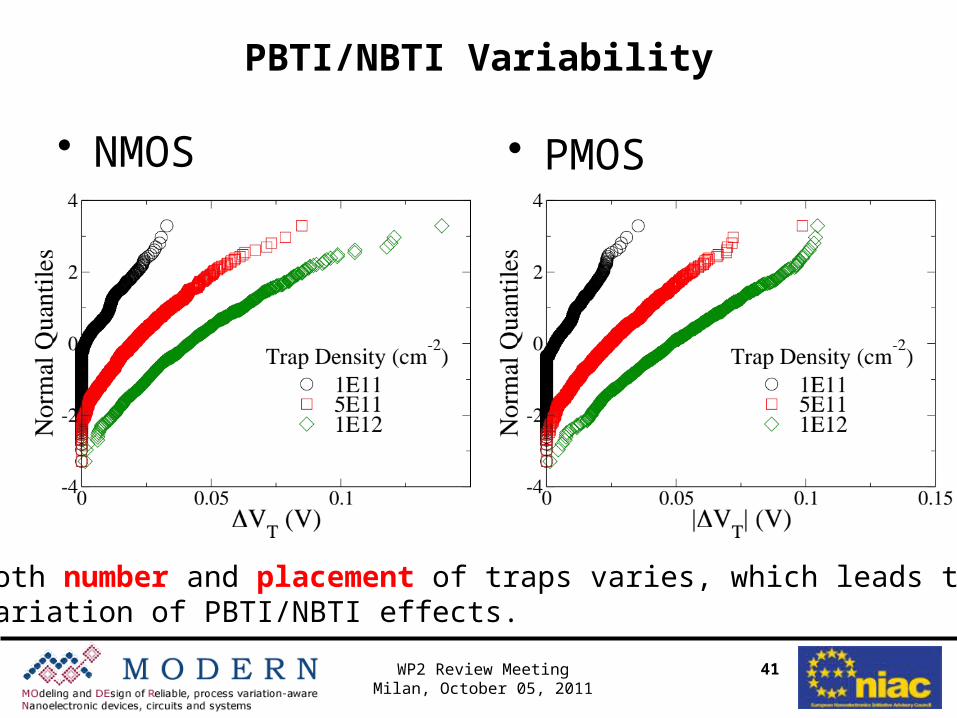
PBTI/NBTI Variability
• NMOS • PMOS
Both number and placement of traps varies, which leads to variation of PBTI/NBTI effects.
42WP2 Review MeetingMilan, October 05, 2011
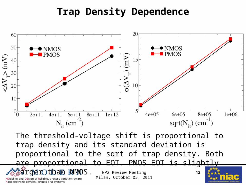
Trap Density Dependence
The threshold-voltage shift is proportional to trap density and its standard deviation is proportional to the sqrt of trap density. Both are proportional to EOT. PMOS EOT is slightly larger than NMOS.
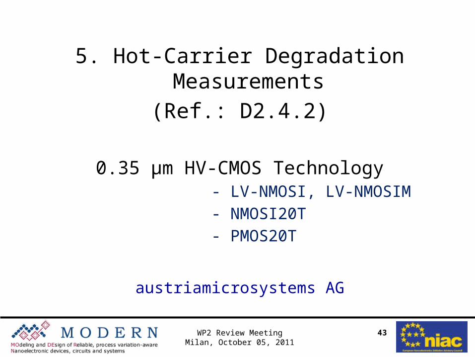
5. Hot-Carrier Degradation Measurements
(Ref.: D2.4.2)
0.35 µm HV-CMOS Technology - LV-NMOSI, LV-NMOSIM
- NMOSI20T
- PMOS20T
austriamicrosystems AG
43WP2 Review MeetingMilan, October 05, 2011
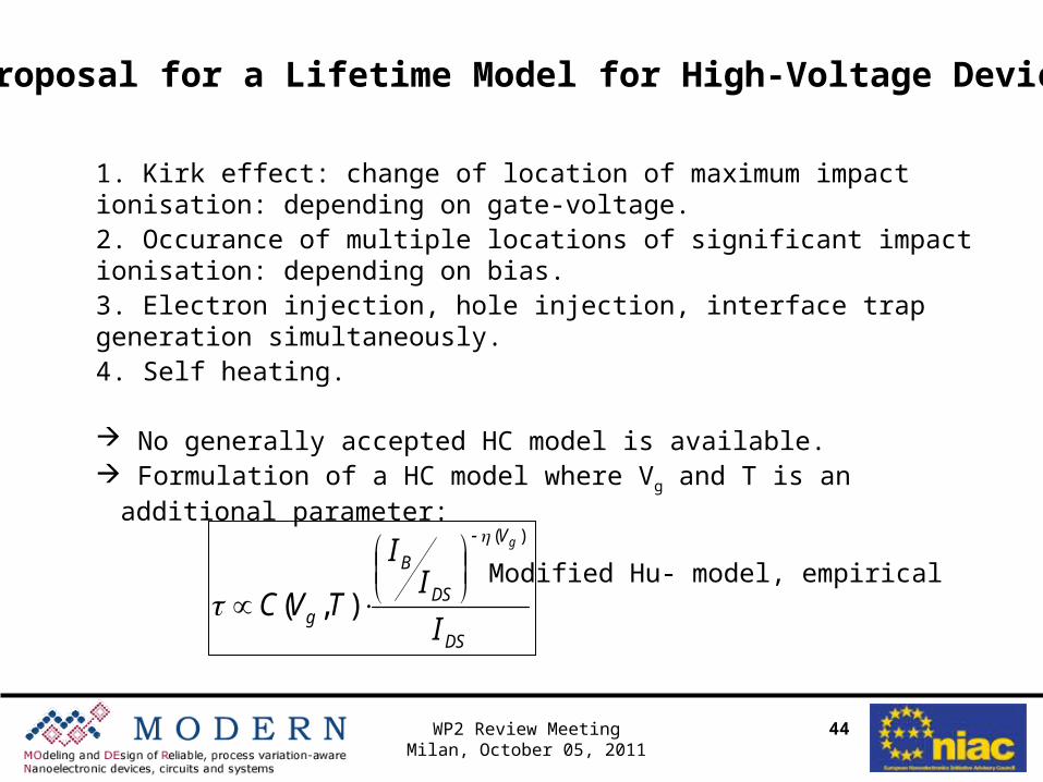
Proposal for a Lifetime Model for High-Voltage Devices
DS
V
DS
B
g I
II
TVC
g )(
),(
Modified Hu- model, empirical
1. Kirk effect: change of location of maximum impact ionisation: depending on gate-voltage.2. Occurance of multiple locations of significant impact ionisation: depending on bias.3. Electron injection, hole injection, interface trap generation simultaneously.4. Self heating.
No generally accepted HC model is available. Formulation of a HC model where Vg and T is an additional parameter:
44WP2 Review MeetingMilan, October 05, 2011
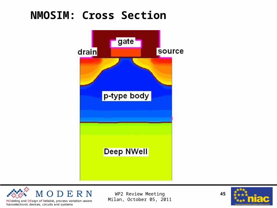
NMOSIM: Cross Section
45WP2 Review MeetingMilan, October 05, 2011
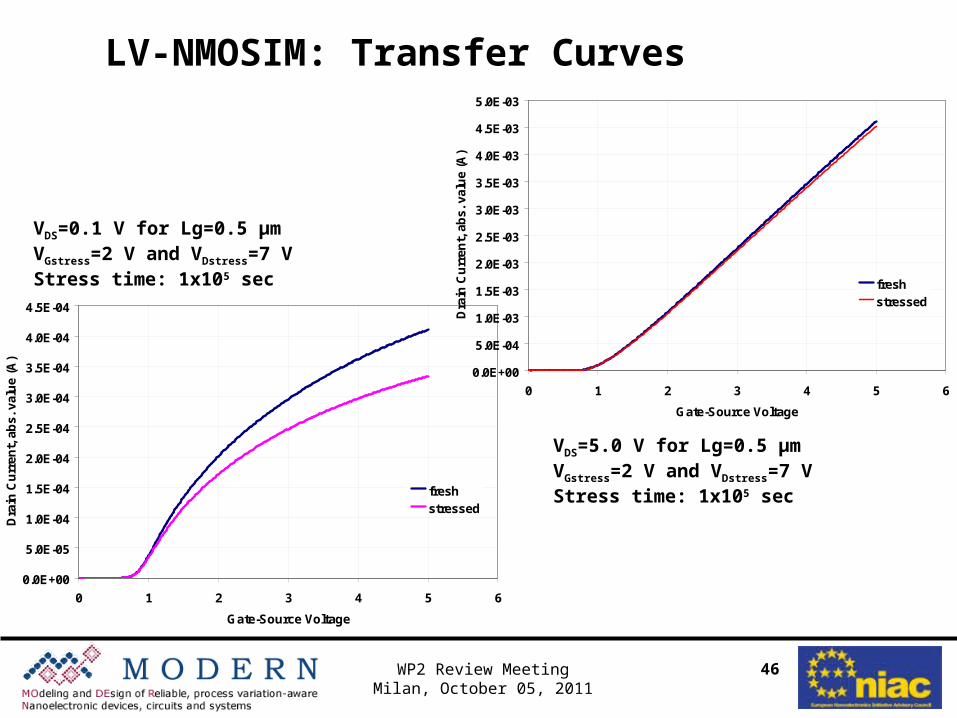
LV-NMOSIM: Transfer Curves
46WP2 Review MeetingMilan, October 05, 2011
0.0E+00
5.0E-05
1.0E-04
1.5E-04
2.0E-04
2.5E-04
3.0E-04
3.5E-04
4.0E-04
4.5E-04
0 1 2 3 4 5 6
Gate-Source Voltage
Dra
in C
urr
ent,
ab
s. v
alu
e (A
)
fresh
stressed
0.0E+00
5.0E-04
1.0E-03
1.5E-03
2.0E-03
2.5E-03
3.0E-03
3.5E-03
4.0E-03
4.5E-03
5.0E-03
0 1 2 3 4 5 6
Gate-Source Voltage
Dra
in C
urr
en
t, a
bs.
val
ue
(A
)
fresh
stressed
VDS=0.1 V for Lg=0.5 µm VGstress=2 V and VDstress=7 VStress time: 1x10⁵ sec
VDS=5.0 V for Lg=0.5 µm VGstress=2 V and VDstress=7 VStress time: 1x10⁵ sec
47WP2 Review MeetingMilan, October 05, 2011
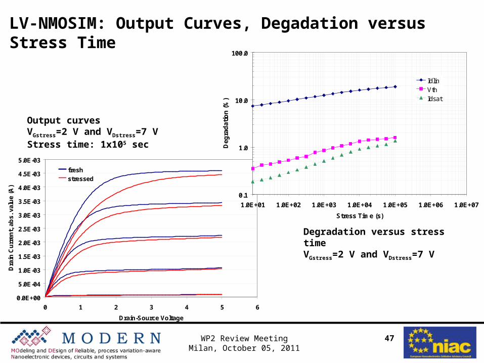
Output curves VGstress=2 V and VDstress=7 VStress time: 1x10⁵ sec
Degradation versus stress time VGstress=2 V and VDstress=7 V
0.0E+00
5.0E-04
1.0E-03
1.5E-03
2.0E-03
2.5E-03
3.0E-03
3.5E-03
4.0E-03
4.5E-03
5.0E-03
0 1 2 3 4 5 6
Drain-Source Voltage
Dra
in C
urr
ent,
ab
s. v
alu
e (A
)
0.0E+00
5.0E-04
1.0E-03
1.5E-03
2.0E-03
2.5E-03
3.0E-03
3.5E-03
4.0E-03
4.5E-03
5.0E-03
0 1 2 3 4 5 6
fresh
stressed
LV-NMOSIM: Output Curves, Degadation versus Stress Time
0.1
1.0
10.0
100.0
1.0E+01 1.0E+02 1.0E+03 1.0E+04 1.0E+05 1.0E+06 1.0E+07
Stress Time (s)
Deg
rad
atio
n (
%)
IdlinVthIdsat
48WP2 Review MeetingMilan, October 05, 2011
y = 1E+14x-5.8222
1.0E+01
1.0E+02
1.0E+03
1.0E+04
1.0E+05
1.0E+06
1.0E+07
1.0E+00 1.0E+01 1.0E+02 1.0E+03
abs(Ibulk)
10%
life
tim
e Id
lin (
s)
1.0E+01
1.0E+02
1.0E+03
1.0E+04
1.0E+05
1.0E+06
1.0E+07
1.0E+08
1.0E+09
1.0E-02 1.0E-01 1.0E+00
abs(Ibulk / Idrain)Id
* li
feti
me
Idlin
(s)
L=2um
L=1.2um
L=0.8um
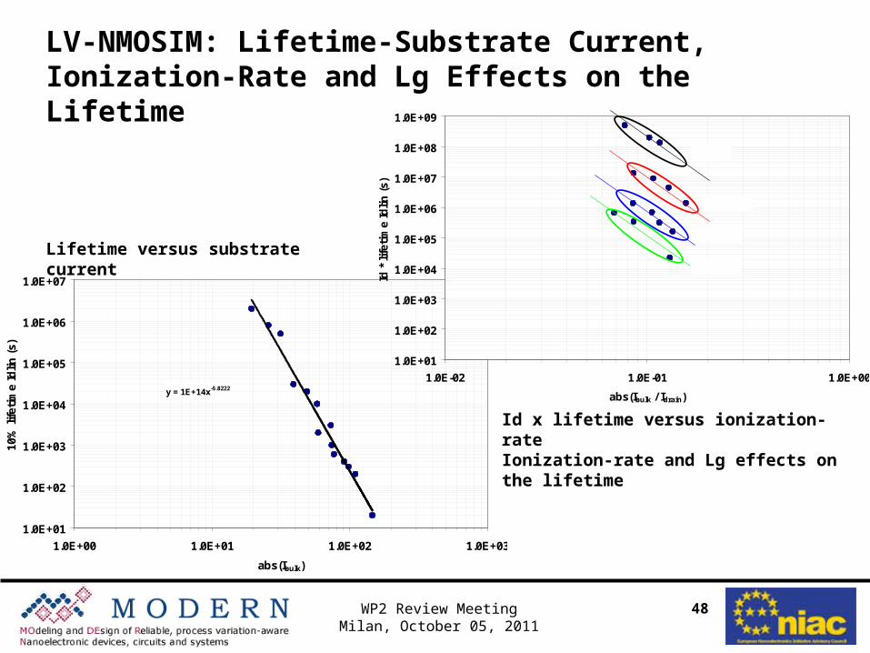
L=0.5umLifetime versus substrate current
Id x lifetime versus ionization-rateIonization-rate and Lg effects on the lifetime
LV-NMOSIM: Lifetime-Substrate Current, Ionization-Rate and Lg Effects on the Lifetime
49WP2 Review MeetingMilan, October 05, 2011
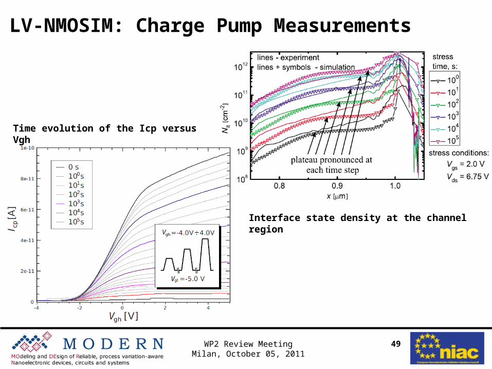
LV-NMOSIM: Charge Pump Measurements
Time evolution of the Icp versus Vgh
Interface state density at the channel region
50WP2 Review MeetingMilan, October 05, 2011
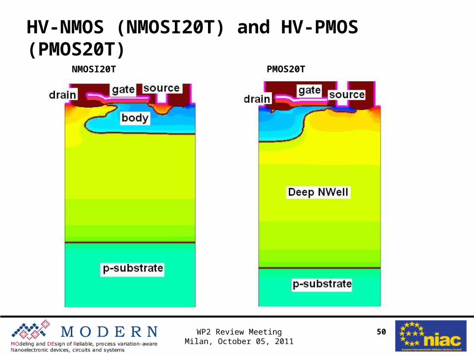
HV-NMOS (NMOSI20T) and HV-PMOS (PMOS20T)
NMOSI20T PMOS20T
51WP2 Review MeetingMilan, October 05, 2011
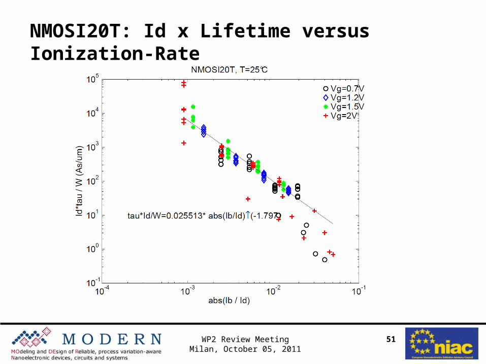
NMOSI20T: Id x Lifetime versus Ionization-Rate
52WP2 Review MeetingMilan, October 05, 2011
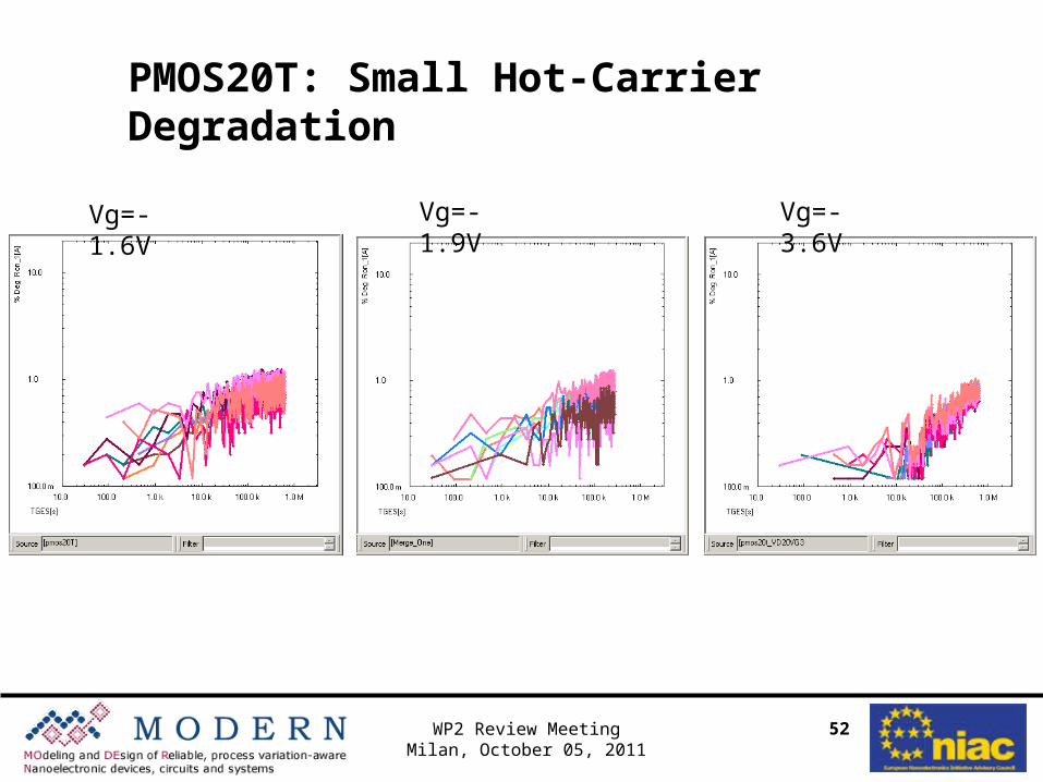
Vg=-1.6V Vg=-1.9V Vg=-3.6V
PMOS20T: Small Hot-Carrier Degradation
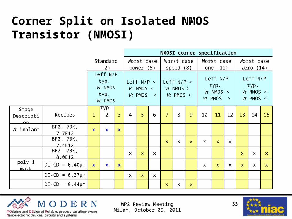
Corner Split on Isolated NMOS Transistor (NMOSI)
53WP2 Review MeetingMilan, October 05, 2011
NMOSI corner specification
Standard (2)Worst casepower (5)
Worst casespeed (8)
Worst caseone (11)
Worst casezero (14)
Leff N/P typ. Vt NMOS typ. Vt PMOS typ.
Leff N/P < Vt NMOS < Vt PMOS <
Leff N/P > Vt NMOS > Vt PMOS >
Leff N/P typ. Vt NMOS <Vt PMOS >
Leff N/P typ. Vt NMOS >Vt PMOS <
Stage Description
Recipes 1 2 3 4 5 6 7 8 9 10 11 12 13 14 15
Vt implant BF2, 70K, 7.7E12 x x x
BF2, 70K, 7.4E12 x x x x x x
BF2, 70K, 8.0E12 x x x x x x
poly 1 mask DI-CD = 0.40µm x x x x x x x x x
DI-CD = 0.37µm x x x
DI-CD = 0.44µm x x x
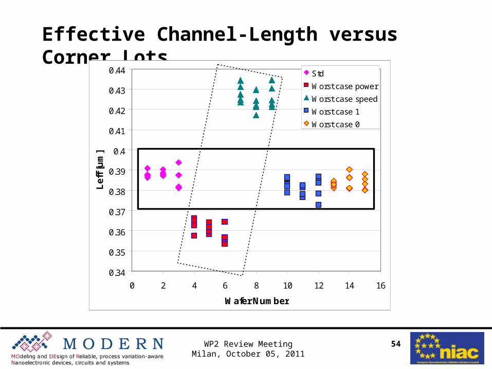
Effective Channel-Length versus Corner Lots
54WP2 Review MeetingMilan, October 05, 2011
0.34
0.35
0.36
0.37
0.38
0.39
0.4
0.41
0.42
0.43
0.44
0 2 4 6 8 10 12 14 16
Wafer Number
Le
ff [
um
]
Std
Worst case power
Worst case speed
Worst case 1
Worst case 0
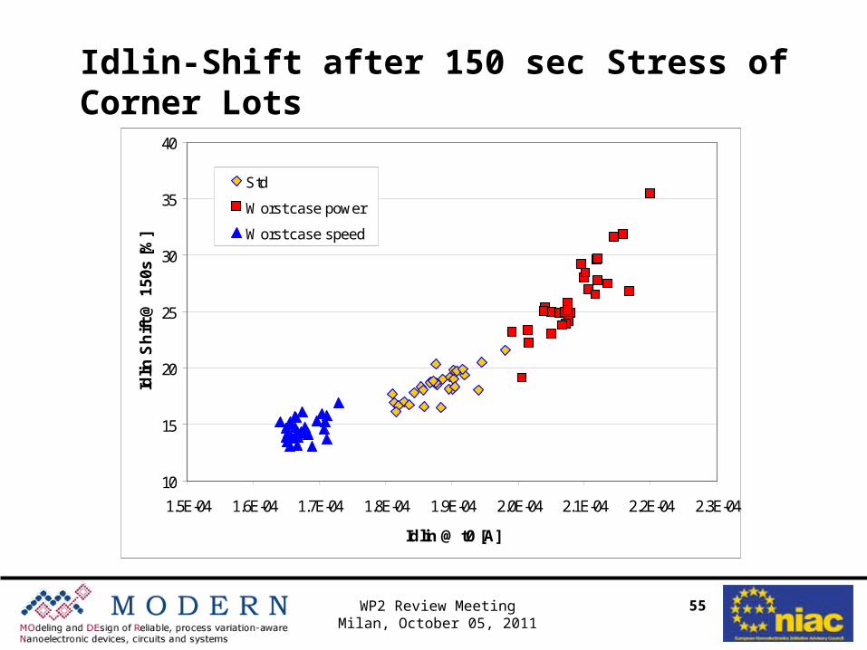
Idlin-Shift after 150 sec Stress of Corner Lots
55WP2 Review MeetingMilan, October 05, 2011
10
15
20
25
30
35
40
1.5E-04 1.6E-04 1.7E-04 1.8E-04 1.9E-04 2.0E-04 2.1E-04 2.2E-04 2.3E-04
Idlin @ t0 [A]
Idlin
Sh
ift
@ 1
50
s [
%]
Std
Worst case power
Worst case speed
56WP2 Review MeetingMilan, October 05, 2011
0
0.5
1
1.5
2
2.5
3
0.0051 0.0052 0.0053 0.0054 0.0055 0.0056 0.0057 0.0058 0.0059 0.006 0.0061
IDsat @ t0 [A]
IDsa
t S
hif
t @
150
s [%
]
Std
Worst case power
Worst case speed
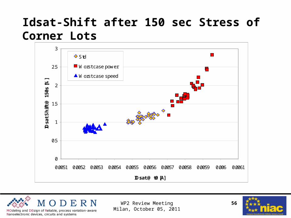
Idsat-Shift after 150 sec Stress of Corner Lots
57WP2 Review MeetingMilan, October 05, 2011
Conclusions
D2.4.1: done - Specification of considered degradation effects, modelling approaches and device parameters - NBTI and HC data (0.35 µm LV-CMOS & HV-CMOS): available for TCAD simulations - Initial physics-based analytical model for NBTI to implement in circuit simulator - Time dependent modeling of degradation for NBTI & HC
D2.4.2 (M24): done - TCAD reliability simulations focused on LV devices in HV-CMOS process - Hot-carrier degradation measurements for analytical & TCAD model developments - Threshold Voltage Mismatch Induced by Hot-Carrier in 65 and 45 nm Technology Node
D2.4.3 (M33): on going
- Statistical compact Models will be extracted at different levels of NBTI and PBTI. - Time dependence of the statistical compact models will be provided based on NBTI and PBTI models of trap charge as a function of time - Analytical NBTI and HC model developments for LV- & HV-CMOS - TCAD reliability simulations focused on HV-CMOS technology - Digital IG noise simulation


![T2.4 [Computer Component- Communication Devices]](https://img.pdfslide.us/doc/110x75/577cde301a28ab9e78ae94f6/t24-computer-component-communication-devices.jpg)