Embed Size (px)
Citation preview
Feature-level Compensation & Control
WorkshopSeptember 6th, 2007
Lithography
A UC Discovery Project
09/06/2007 FLCC - Lithography
2
FLCC
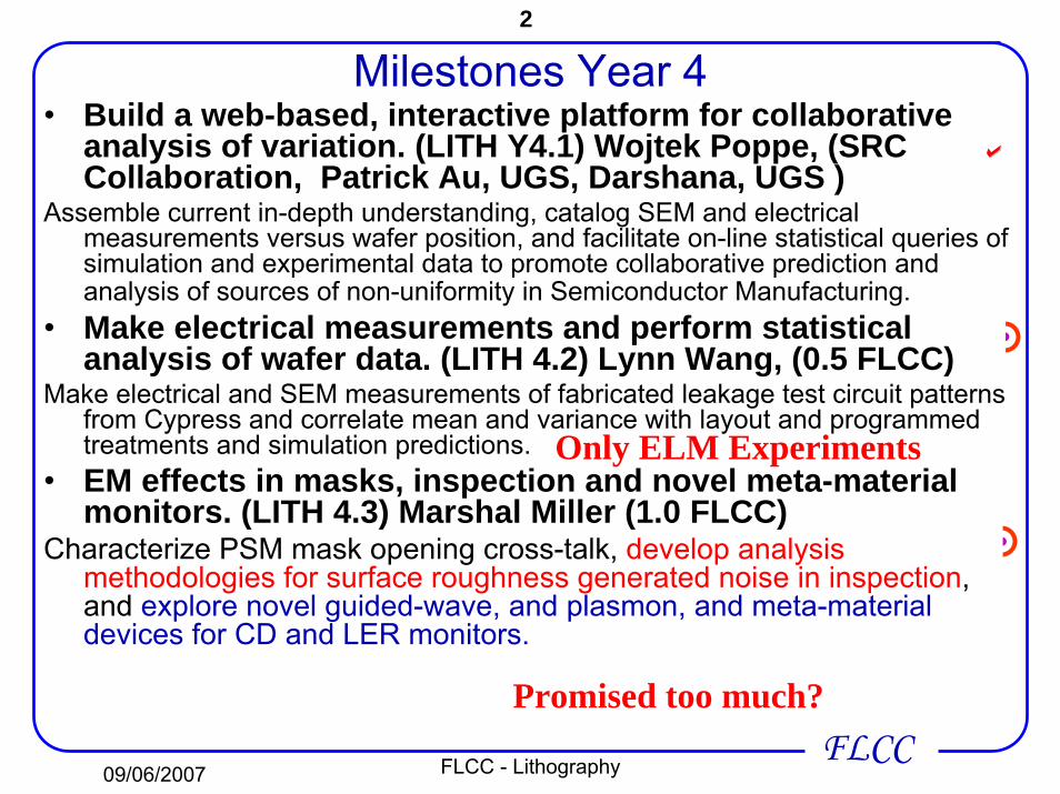
• Build a web-based, interactive platform for collaborative analysis of variation. (LITH Y4.1) Wojtek Poppe, (SRC Collaboration, Patrick Au, UGS, Darshana, UGS )
Assemble current in-depth understanding, catalog SEM and electrical measurements versus wafer position, and facilitate on-line statistical queries of simulation and experimental data to promote collaborative prediction and analysis of sources of non-uniformity in Semiconductor Manufacturing.
• Make electrical measurements and perform statistical analysis of wafer data. (LITH 4.2) Lynn Wang, (0.5 FLCC)
Make electrical and SEM measurements of fabricated leakage test circuit patterns from Cypress and correlate mean and variance with layout and programmed treatments and simulation predictions.
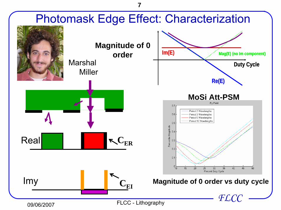
• EM effects in masks, inspection and novel meta-material monitors. (LITH 4.3) Marshal Miller (1.0 FLCC)
Characterize PSM mask opening cross-talk, develop analysis methodologies for surface roughness generated noise in inspection, and explore novel guided-wave, and plasmon, and meta-material devices for CD and LER monitors.
Milestones Year 4
Only ELM Experiments
Promised too much?
09/06/2007 FLCC - Lithography
3
FLCC
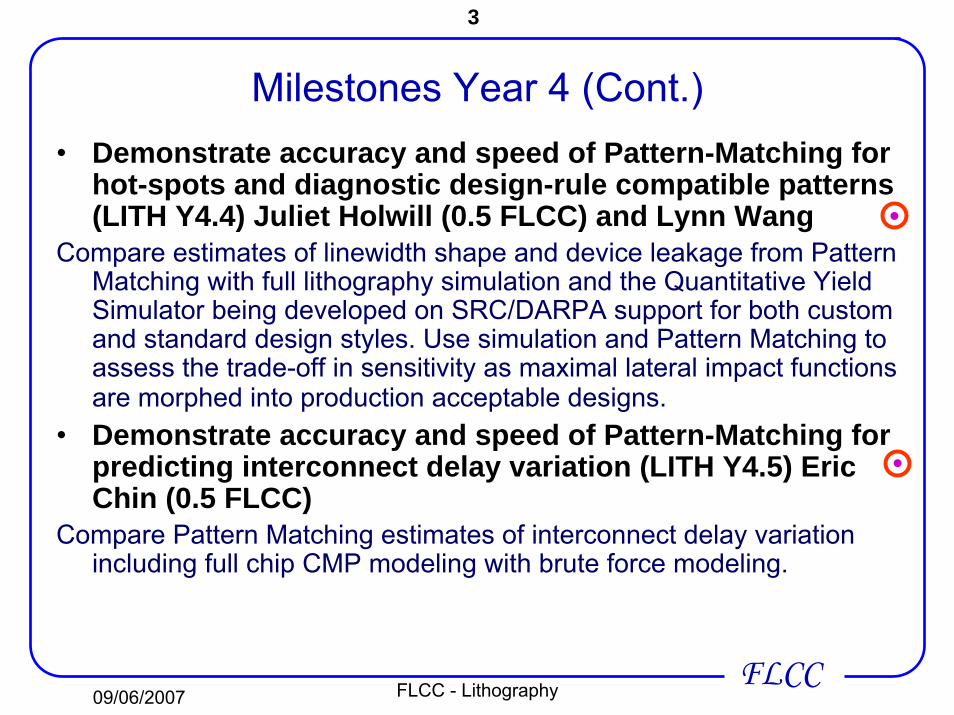
Milestones Year 4 (Cont.)• Demonstrate accuracy and speed of Pattern-Matching for
hot-spots and diagnostic design-rule compatible patterns (LITH Y4.4) Juliet Holwill (0.5 FLCC) and Lynn Wang
Compare estimates of linewidth shape and device leakage from Pattern Matching with full lithography simulation and the Quantitative Yield Simulator being developed on SRC/DARPA support for both custom and standard design styles. Use simulation and Pattern Matching to assess the trade-off in sensitivity as maximal lateral impact functions are morphed into production acceptable designs.
• Demonstrate accuracy and speed of Pattern-Matching for predicting interconnect delay variation (LITH Y4.5) Eric Chin (0.5 FLCC)
Compare Pattern Matching estimates of interconnect delay variation including full chip CMP modeling with brute force modeling.
09/06/2007 FLCC - Lithography
4
FLCC
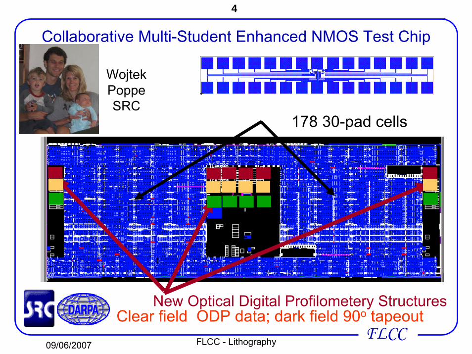
Collaborative Multi-Student Enhanced NMOS Test Chip
178 30-pad cells
Clear field ODP data; dark field 90o tapeoutNew Optical Digital Profilometery Structures
Wojtek Poppe SRC
09/06/2007 FLCC - Lithography
5
FLCC
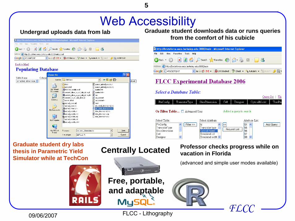
Web AccessibilityUndergrad uploads data from lab Graduate student downloads data or runs queries
from the comfort of his cubicle
Centrally Located
Free, portable, and adaptable
Professor checks progress while on vacation in Florida(advanced and simple user modes available)
Graduate student dry labs thesis in Parametric Yield Simulator while at TechCon
09/06/2007 FLCC - Lithography
6
FLCC
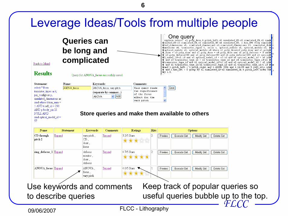
Leverage Ideas/Tools from multiple peopleQueries can be long and complicated
Store queries and make them available to others
Keep track of popular queries so useful queries bubble up to the top.
One query
Use keywords and comments to describe queries
09/06/2007 FLCC - Lithography
7
FLCC
Photomask Edge Effect: Characterization
Imy CEI
Real CER
Magnitude of 0 order vs duty cycle
MoSi Att-PSM
Marshal Miller
Re(E)
Im(E)
Duty Cycle
Mag(E) (no Im component)
Re(E)
Im(E)
Duty Cycle
Mag(E) (no Im component)Magnitude of 0
order
09/06/2007 FLCC - Lithography
8
FLCC
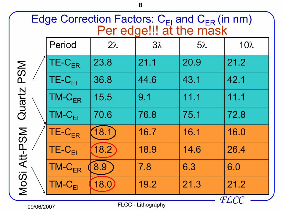
Edge Correction Factors: CEI and CER (in nm)
Period 2λ 3λ 5λ 10λ
TE-CER 23.8 21.1 20.9 21.2
TE-CEI 36.8 44.6 43.1 42.1
TM-CER 15.5 9.1 11.1 11.1
TM-CEI 70.6 76.8 75.1 72.8
TE-CER 18.1 16.7 16.1 16.0
TE-CEI 18.2 18.9 14.6 26.4
TM-CER 8.9 7.8 6.3 6.0
TM-CEI 18.0 19.2 21.3 21.2
Per edge!!! at the maskQ
uartz
PS
MM
oSiA
tt-P
SM
09/06/2007 FLCC - Lithography
9
FLCC
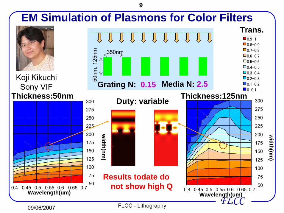
EM Simulation of Plasmons for Color Filters
Grating N: 0.15 Media N: 2.5
350nm
50nm
, 125
nmDuty: variable
50
75
100
125
150
175
200
225
250
275
300
width(nm
)0.4 0.45 0.5 0.55 0.6 0.65 0.7
Wavelength(um) 0.4 0.45 0.5 0.55 0.6 0.65 0.7Wavelength(um)
50
75
100
125
150
175
200
225
250
275
300
width(nm
)
0.9-1
0.8-0.9
0.7-0.8
0.6-0.7
0.5-0.6
0.4-0.5
0.3-0.4
0.2-0.3
0.1-0.2
0-0.1
Trans.
Thickness:50nm Thickness:125nm
Koji KikuchiSony VIF
Results todate do not show high Q
09/06/2007 FLCC - Lithography
10
FLCC
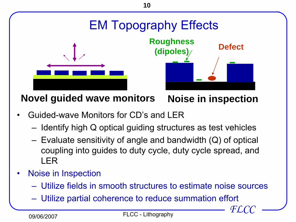
EM Topography Effects Defect
• Guided-wave Monitors for CD’s and LER– Identify high Q optical guiding structures as test vehicles– Evaluate sensitivity of angle and bandwidth (Q) of optical
coupling into guides to duty cycle, duty cycle spread, and LER
• Noise in Inspection– Utilize fields in smooth structures to estimate noise sources– Utilize partial coherence to reduce summation effort
Roughness(dipoles)
Novel guided wave monitors Noise in inspection
09/06/2007 FLCC - Lithography
11
FLCC
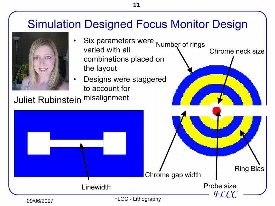
Simulation Designed Focus Monitor Design
Chrome gap width
Chrome neck sizeNumber of rings• Six parameters were
varied with all combinations placed on the layout
• Designs were staggered to account for misalignment
Ring Bias
Juliet Rubinstein
Probe sizeLinewidth
09/06/2007 FLCC - Lithography
12
FLCC
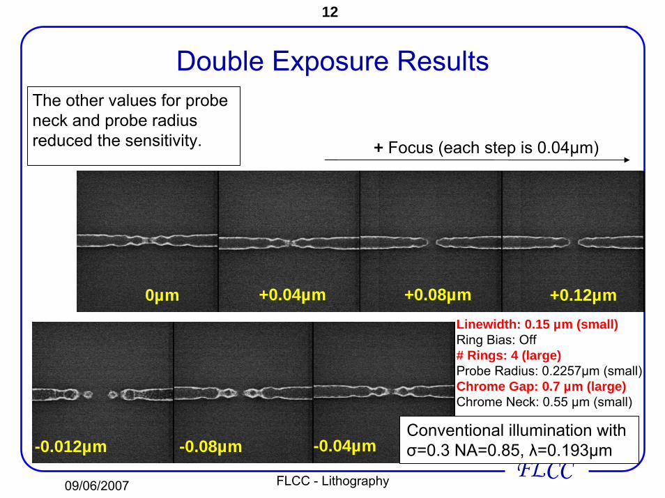
Double Exposure ResultsThe other values for probe neck and probe radius reduced the sensitivity.
-0.04µm-0.08µm-0.012µm
+ Focus (each step is 0.04µm)
0µm +0.04µm +0.08µm +0.12µm
Conventional illumination with σ=0.3 NA=0.85, λ=0.193µm
Linewidth: 0.15 µm (small)Ring Bias: Off # Rings: 4 (large)Probe Radius: 0.2257µm (small)Chrome Gap: 0.7 µm (large)Chrome Neck: 0.55 µm (small)
09/06/2007 FLCC - Lithography
13
FLCC
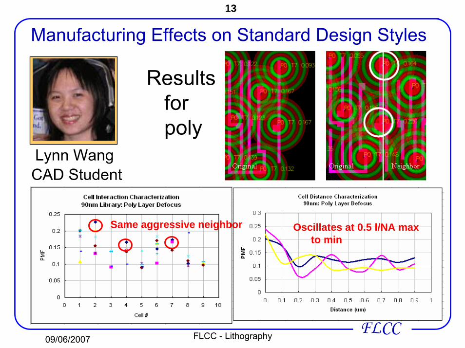
Manufacturing Effects on Standard Design Styles
Your Photo Here
Lynn WangCAD Student
0.5um Separation0.2um Separation
Results for poly
Same aggressive neighbor Oscillates at 0.5 l/NA max to min
09/06/2007 FLCC - Lithography
14
FLCC
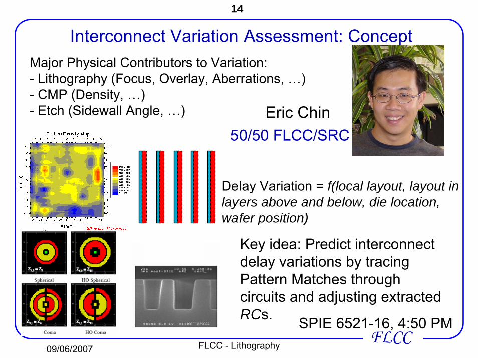
Interconnect Variation Assessment: ConceptMajor Physical Contributors to Variation:- Lithography (Focus, Overlay, Aberrations, …)- CMP (Density, …)- Etch (Sidewall Angle, …)
Key idea: Predict interconnect delay variations by tracing Pattern Matches through circuits and adjusting extracted RCs.
Delay Variation = f(local layout, layout in layers above and below, die location, wafer position)
Eric Chin
SPIE 6521-16, 4:50 PM
50/50 FLCC/SRC
09/06/2007 FLCC - Lithography
15
FLCC
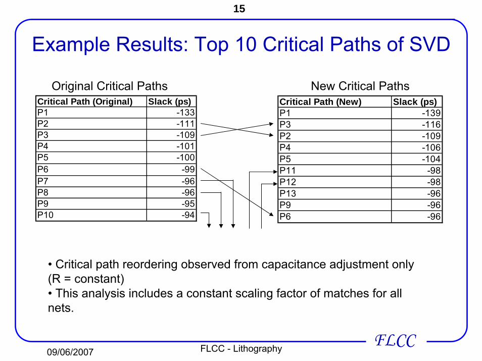
Example Results: Top 10 Critical Paths of SVD
Original Critical Paths New Critical PathsCritical Path (Original) Slack (ps)P1 -133P2 -111P3 -109P4 -101P5 -100P6 -99P7 -96P8 -96P9 -95P10 -94
Critical Path (New) Slack (ps)P1 -139P3 -116P2 -109P4 -106P5 -104P11 -98P12 -98P13 -96P9 -96P6 -96
• Critical path reordering observed from capacitance adjustment only (R = constant)• This analysis includes a constant scaling factor of matches for all nets.
09/06/2007 FLCC - Lithography
16
FLCC
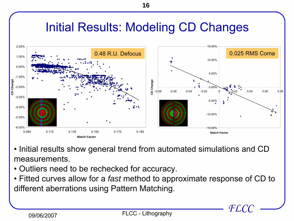
Initial Results: Modeling CD Changes
-6.00%
-5.00%
-4.00%
-3.00%
-2.00%
-1.00%
0.00%
1.00%
2.00%
0.095 0.115 0.135 0.155 0.175 0.195
Match Factor
CD
Cha
nge
-15.00%
-10.00%
-5.00%
0.00%
5.00%
10.00%
15.00%
-0.08 -0.06 -0.04 -0.02 0 0.02 0.04 0.06 0.08
Match Factor
CD
Cha
nge
0.48 R.U. Defocus 0.025 RMS Coma
• Initial results show general trend from automated simulations and CD measurements.• Outliers need to be rechecked for accuracy.• Fitted curves allow for a fast method to approximate response of CD to different aberrations using Pattern Matching.
09/06/2007 FLCC - Lithography
17
FLCC
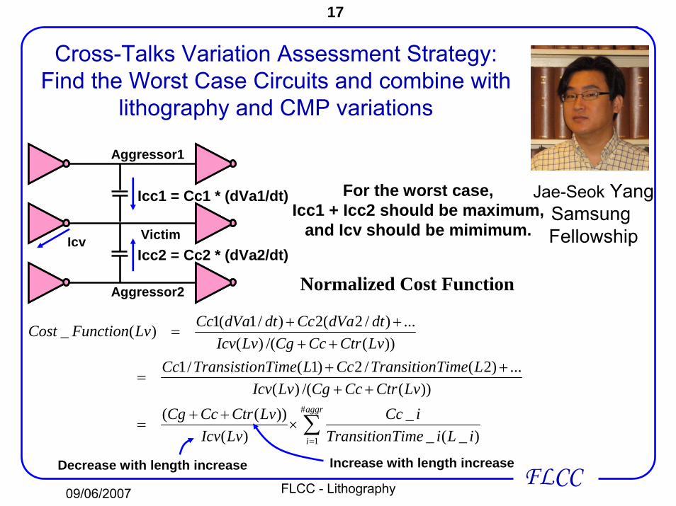
Cross-Talks Variation Assessment Strategy: Find the Worst Case Circuits and combine with
lithography and CMP variations
Jae-Seok YangSamsung FellowshipVictim
Aggressor1
Aggressor2
Icc1 = Cc1 * (dVa1/dt)
Icc2 = Cc2 * (dVa2/dt)
For the worst case,Icc1 + Icc2 should be maximum,
and Icv should be mimimum.Icv
∑=
×++
=
++++
=
++++
=
aggr
i iLiTimeTransitioniCc
LvIcvLvCtrCcCg
LvCtrCcCgLvIcvLTimeTransitionCcLnTimeTransistioCc
LvCtrCcCgLvIcvdtdVaCcdtdVaCcLvFunctionCost
#
1 )_(__
)())((
))(/()(...)2(/2)1(/1
))(/()(...)/2(2)/1(1)(_
Increase with length increaseDecrease with length increase
Normalized Cost Function
09/06/2007 FLCC - Lithography
18
FLCC
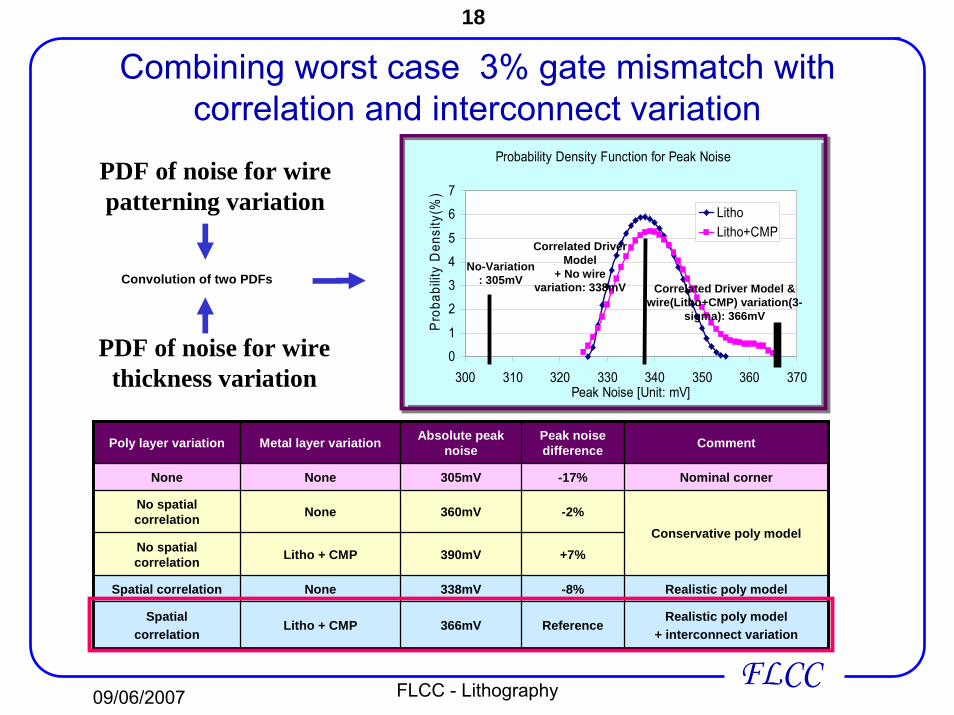
Combining worst case 3% gate mismatch with correlation and interconnect variation
=
Probability Density Function for Peak Noise
0
1
2
3
4
5
6
7
300 310 320 330 340 350 360 370Peak Noise [Unit: mV]
Pro
babi
lity
Den
sity
(%)
LithoLitho+CMP
Probability Density Function for Peak Noise
0
1
2
3
4
5
6
7
300 310 320 330 340 350 360 370Peak Noise [Unit: mV]
Pro
babi
lity
Den
sity
(%)
LithoLitho+CMP
No-Variation : 305mV
Correlated Driver Model
+ No wire variation: 338mV Correlated Driver Model &
wire(Litho+CMP) variation(3-sigma): 366mV
+7%390mVLitho + CMPNo spatial correlation
Reference
-8%
-2%
-17%
Peak noise difference
Realistic poly model+ interconnect variation
366mVLitho + CMPSpatial
correlation
Realistic poly model338mVNoneSpatial correlation
Conservative poly model360mVNoneNo spatial
correlation
Nominal corner305mVNoneNone
CommentAbsolute peak noiseMetal layer variationPoly layer variation
Convolution of two PDFs
PDF of noise for wirepatterning variation
PDF of noise for wirethickness variation
09/06/2007 FLCC - Lithography
19
FLCC
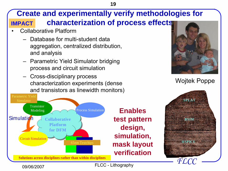
Create and experimentally verify methodologies for characterization of process effects
• Collaborative Platform– Database for multi-student data
aggregation, centralized distribution, and analysis
– Parametric Yield Simulator bridging process and circuit simulation
– Cross-disciplinary process characterization experiments (dense and transistors as linewidth monitors)
Wojtek Poppe
SPLAT
BSIM
HSPICE
SPLAT
BSIM
HSPICE
Collaborative Platformfor DFM
Collaborative Platformfor DFM
Circuit Simulation
Transistor Modeling Process Simulation
Circuit Simulation
Transistor Modeling Process Simulation
65nm Testchips
Simulation
Parametric Yield Simulator
Solutions across disciplines rather than within disciplines
Enables test pattern
design, simulation, mask layoutverification
IMPACT
09/06/2007 FLCC - Lithography
20
FLCC
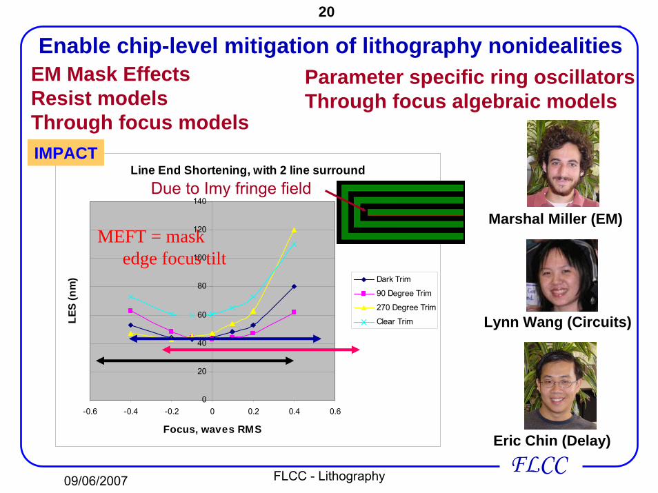
Enable chip-level mitigation of lithography nonidealitiesEM Mask EffectsResist modelsThrough focus models
Parameter specific ring oscillatorsThrough focus algebraic models
Line End Shortening, with 2 line surround
0
20
40
60
80
100
120
140
-0.6 -0.4 -0.2 0 0.2 0.4 0.6
Focus, waves RMS
LES
(nm
) Dark Trim
90 Degree Trim
270 Degree Trim
Clear Trim
Due to Imy fringe field
MEFT = mask edge focus tilt
IMPACT
Marshal Miller (EM)
Lynn Wang (Circuits)
Eric Chin (Delay)
09/06/2007 FLCC - Lithography
21
FLCC
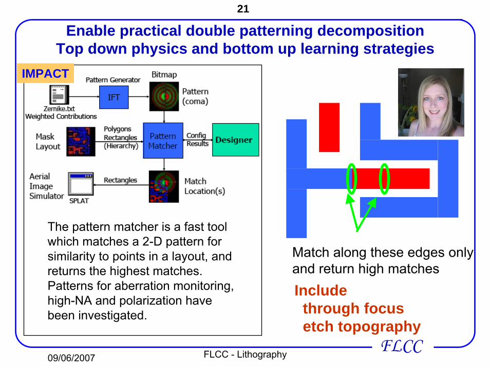
Enable practical double patterning decompositionTop down physics and bottom up learning strategies
The pattern matcher is a fast tool which matches a 2-D pattern for similarity to points in a layout, and returns the highest matches. Patterns for aberration monitoring, high-NA and polarization have been investigated.
IMPACT
Match along these edges only and return high matchesIncludethrough focusetch topography
09/06/2007 FLCC - Lithography
22
FLCC
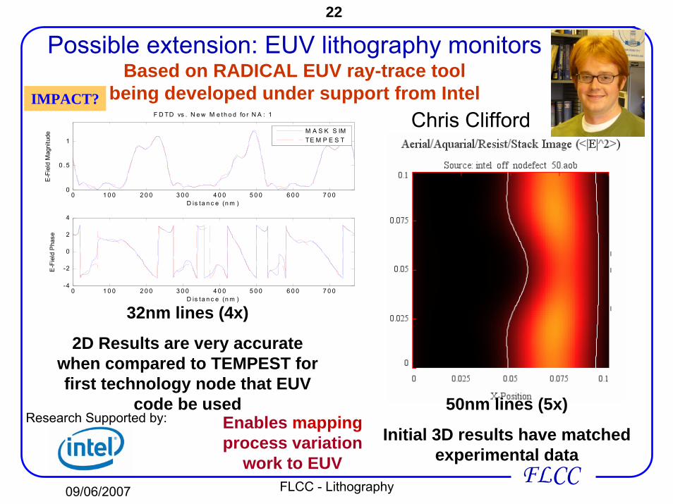
0 1 0 0 2 0 0 3 0 0 4 0 0 5 0 0 6 0 0 7 0 00
0 . 5
1
D is ta n c e (n m )
E-F
ield
Mag
nitu
de
F D TD vs . N e w M e th o d fo r N A : 1
M A S K S IMTE M P E S T
0 1 0 0 2 0 0 3 0 0 4 0 0 5 0 0 6 0 0 7 0 0-4
-2
0
2
4
D is ta n c e (n m )
E-F
ield
Pha
se
32nm lines (4x)
2D Results are very accurate when compared to TEMPEST for first technology node that EUV
code be used
Possible extension: EUV lithography monitorsBased on RADICAL EUV ray-trace tool
being developed under support from Intel
50nm lines (5x)
Initial 3D results have matched experimental data
Research Supported by:
Chris Clifford
Enables mappingprocess variation
work to EUV
IMPACT?
09/06/2007 FLCC - Lithography
23
FLCC
Lithography Research in IMPACT• Create and experimentally verify methodologies for
characterization of process effects on patterning, pattern transfer, and circuit performance
– Simulation based design; test mask layout – Experiments with systematically program various nonidealities
such as focus, trefoil, illumination and likely LER.• Enable chip-level mitigation of lithography nonidealities
– first principles modeling of masks and imaging, – developing fast-CAD first-cut accurate models, – designing electrical circuit performance monitors
• Enable practical double patterning decomposition– Top down lithography effects - through focus – hard mask etch effects state dependent modeling
• Extensions Possible– EUV lithography monitors (Radical infrastructure from Intel?)– EM Simulation of topography inspection