Embed Size (px)
Citation preview
Release 2015.0 April 16, 2015 1 © 2015 ANSYS, Inc.
2015.0 Release
Workshop 3-1: Coax-Microstrip Transition
Introduction to ANSYS HFSS
Release 2015.0 April 16, 2015 2 © 2015 ANSYS, Inc.
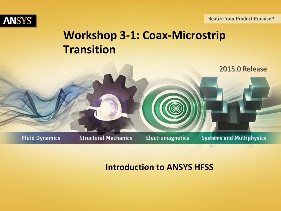
Example – Coax to Microstrip Transition
• Analysis of a Microstrip Transmission Line with SMA Edge Connector • This example is intended to show you how to create and analyze a coax to microstrip transition using ANSYS HFSS.
Release 2015.0 April 16, 2015 3 © 2015 ANSYS, Inc.
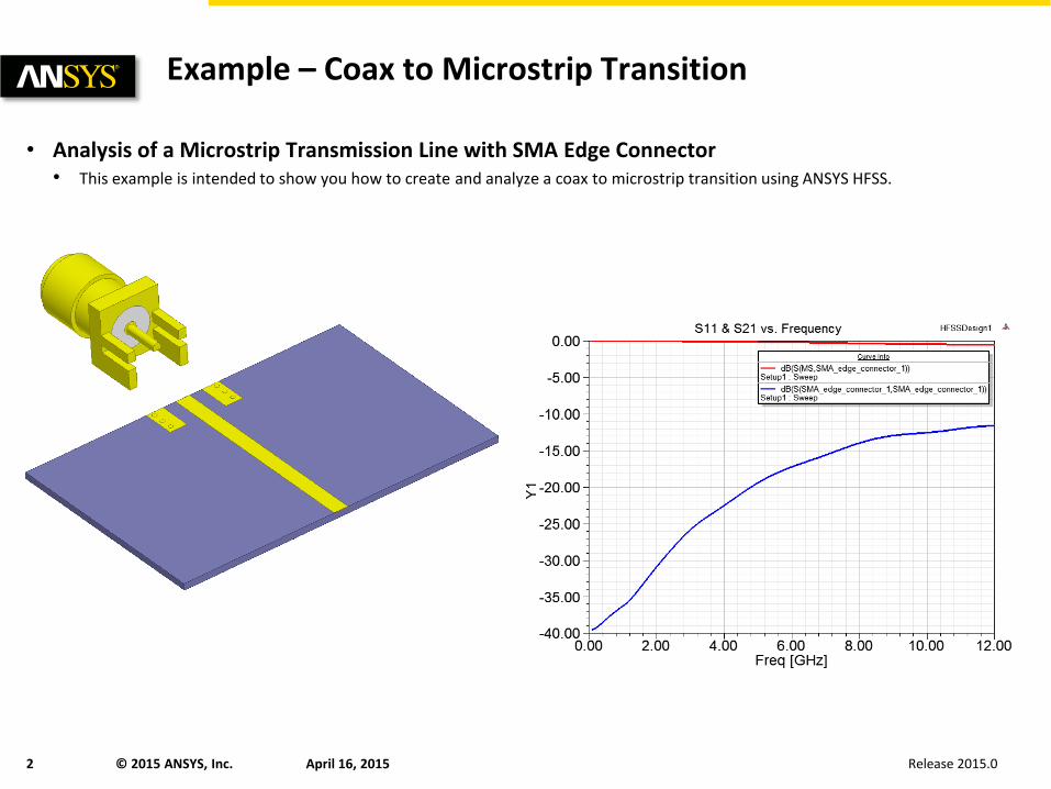
Model Description
• Properties: • Connector
• SMA connector: HFSS 3D Component SMA_edge_connector.a3dcomp
• Printed Circuit Board • Microstrip: PCB.aedt • Substrate: RO4350™ • Substrate Size: 1 in x 1.5 in x 0.030 in • Trace Thickness: 0.7 mil (1/2oz Cu) • Connector Pads: Footprint with Ground Vias
Release 2015.0 April 16, 2015 4 © 2015 ANSYS, Inc.
HFSS: Getting Started
• Launching ANSYS Electronics Desktop 2015 • To access ANSYS Electronics Desktop, click the Microsoft Start button, select Programs > ANSYS Electromagnetics > ANSYS
Electromagnetics Suite 16.0 > ANSYS Electronics Desktop 2015
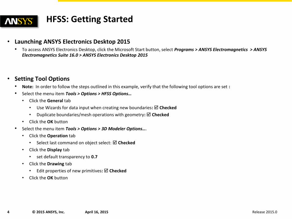
• Setting Tool Options • Note: In order to follow the steps outlined in this example, verify that the following tool options are set :
• Select the menu item Tools > Options > HFSS Options…
• Click the General tab
• Use Wizards for data input when creating new boundaries: Checked
• Duplicate boundaries/mesh operations with geometry: Checked
• Click the OK button
• Select the menu item Tools > Options > 3D Modeler Options….
• Click the Operation tab
• Select last command on object select: Checked
• Click the Display tab
• set default transparency to 0.7
• Click the Drawing tab
• Edit properties of new primitives: Checked
• Click the OK button
Release 2015.0 April 16, 2015 5 © 2015 ANSYS, Inc.
Creating the Design
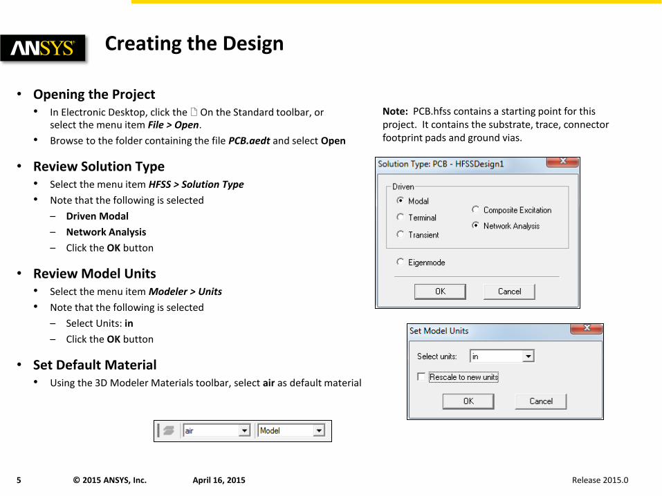
• Opening the Project • In Electronic Desktop, click the On the Standard toolbar, or
select the menu item File > Open.
• Browse to the folder containing the file PCB.aedt and select Open
• Review Solution Type • Select the menu item HFSS > Solution Type
• Note that the following is selected
– Driven Modal
– Network Analysis
– Click the OK button
• Review Model Units • Select the menu item Modeler > Units
• Note that the following is selected
– Select Units: in
– Click the OK button
• Set Default Material • Using the 3D Modeler Materials toolbar, select air as default material
Note: PCB.hfss contains a starting point for this project. It contains the substrate, trace, connector footprint pads and ground vias.
Release 2015.0 April 16, 2015 6 © 2015 ANSYS, Inc.
Design Documentation - Optional
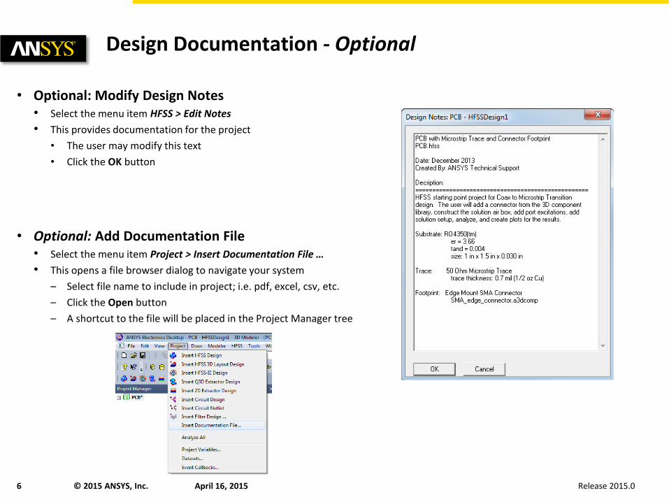
• Optional: Modify Design Notes • Select the menu item HFSS > Edit Notes
• This provides documentation for the project
• The user may modify this text
• Click the OK button
• Optional: Add Documentation File • Select the menu item Project > Insert Documentation File …
• This opens a file browser dialog to navigate your system
– Select file name to include in project; i.e. pdf, excel, csv, etc.
– Click the Open button
– A shortcut to the file will be placed in the Project Manager tree
Release 2015.0 April 16, 2015 7 © 2015 ANSYS, Inc.
Informational: Project Organization
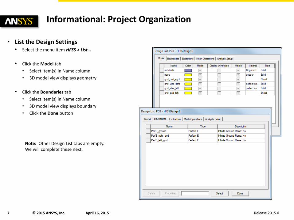
• List the Design Settings • Select the menu item HFSS > List…
• Click the Model tab
• Select item(s) in Name column
• 3D model view displays geometry
• Click the Boundaries tab
• Select item(s) in Name column
• 3D model view displays boundary
• Click the Done button
Note: Other Design List tabs are empty. We will complete these next.
Release 2015.0 April 16, 2015 8 © 2015 ANSYS, Inc.
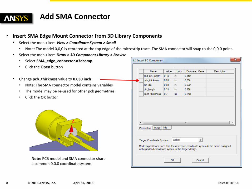
Add SMA Connector
• Insert SMA Edge Mount Connector from 3D Library Components • Select the menu item View > Coordinate System > Small
• Note: The model 0,0,0 is centered at the top edge of the microstrip trace. The SMA connector will snap to the 0,0,0 point.
• Select the menu item Draw > 3D Component Library > Browse
• Select SMA_edge_connector.a3dcomp
• Click the Open button
• Change pcb_thickness value to 0.030 inch
• Note: The SMA connector model contains variables
• The model may be re-used for other pcb geometries
• Click the OK button
Note: PCB model and SMA connector share a common 0,0,0 coordinate system.
Release 2015.0 April 16, 2015 9 © 2015 ANSYS, Inc.
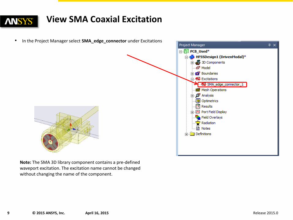
View SMA Coaxial Excitation
• In the Project Manager select SMA_edge_connector under Excitations
Note: The SMA 3D library component contains a pre-defined waveport excitation. The excitation name cannot be changed without changing the name of the component.
Release 2015.0 April 16, 2015 10 © 2015 ANSYS, Inc.
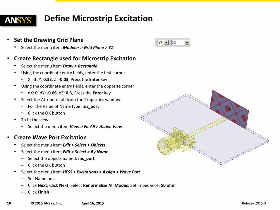
Define Microstrip Excitation
• Set the Drawing Grid Plane • Select the menu item Modeler > Grid Plane > YZ
• Create Rectangle used for Microstrip Excitation • Select the menu item Draw > Rectangle
• Using the coordinate entry fields, enter the first corner
• X: -1, Y: 0.33, Z: -0.03, Press the Enter key
• Using the coordinate entry fields, enter the opposite corner
• dX: 0, dY: -0.66, dZ: 0.3, Press the Enter key
• Select the Attribute tab from the Properties window.
• For the Value of Name type: ms_port
• Click the OK button
• To fit the view:
• Select the menu item View > Fit All > Active View
• Create Wave Port Excitation • Select the menu item Edit > Select > Objects
• Select the menu item Edit > Select > By Name
– Select the objects named: ms_port
– Click the OK button
• Select the menu item HFSS > Excitations > Assign > Wave Port
– Set Name: ms
– Click Next; Click Next; Select Renormalize All Modes; Set Impedance: 50 ohm
– Click Finish
Release 2015.0 April 16, 2015 11 © 2015 ANSYS, Inc.
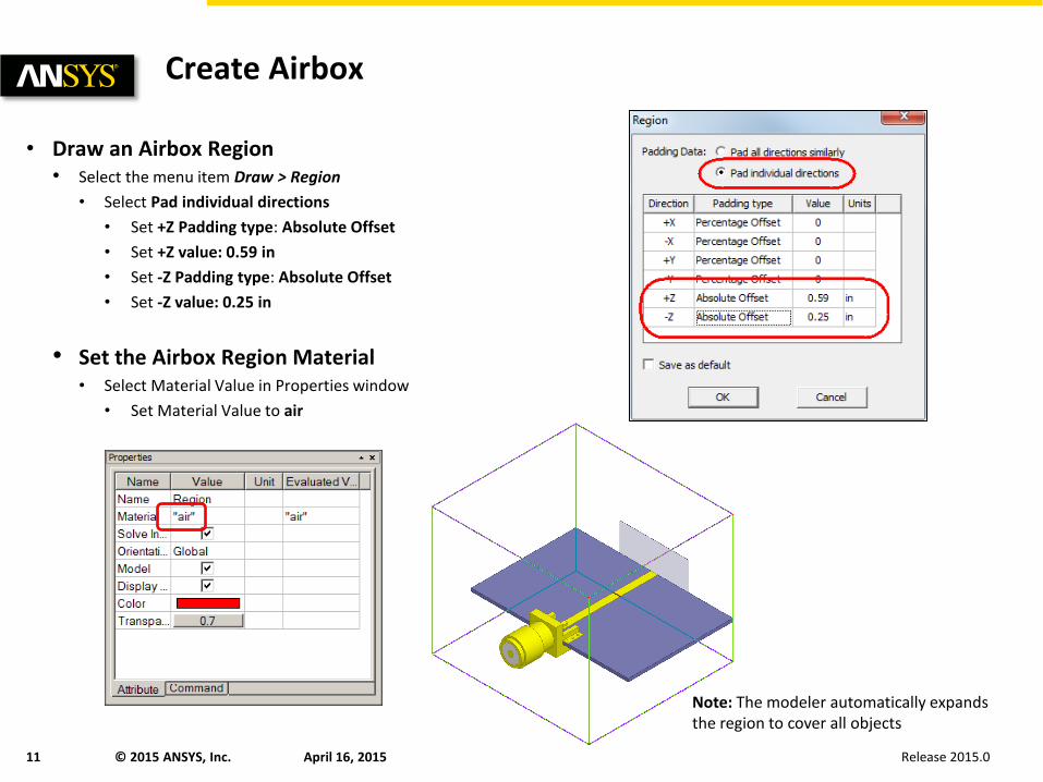
Create Airbox
• Draw an Airbox Region • Select the menu item Draw > Region
• Select Pad individual directions
• Set +Z Padding type: Absolute Offset
• Set +Z value: 0.59 in
• Set -Z Padding type: Absolute Offset
• Set -Z value: 0.25 in
• Set the Airbox Region Material • Select Material Value in Properties window
• Set Material Value to air
Note: The modeler automatically expands the region to cover all objects
Release 2015.0 April 16, 2015 12 © 2015 ANSYS, Inc.
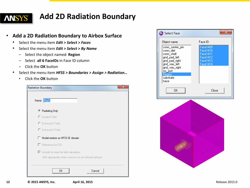
Add 2D Radiation Boundary
• Add a 2D Radiation Boundary to Airbox Surface • Select the menu item Edit > Select > Faces
• Select the menu item Edit > Select > By Name
– Select the object named: Region
– Select all 6 FaceIDs in Face ID column
– Click the OK button
• Select the menu item HFSS > Boundaries > Assign > Radiation…
• Click the OK button
Release 2015.0 April 16, 2015 13 © 2015 ANSYS, Inc.
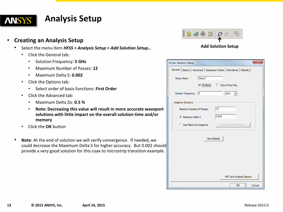
Analysis Setup
• Creating an Analysis Setup • Select the menu item HFSS > Analysis Setup > Add Solution Setup…
• Click the General tab:
• Solution Frequency: 5 GHz
• Maximum Number of Passes: 12
• Maximum Delta S: 0.002
• Click the Options tab:
• Select order of basis functions: First Order
• Click the Advanced tab:
• Maximum Delta Zo: 0.5 %
• Note: Decreasing this value will result in more accurate waveport solutions with little impact on the overall solution time and/or memory
• Click the OK button
• Note: At the end of solution we will verify convergence. If needed, we could decrease the Maximum Delta S for higher accuracy. But 0.002 should provide a very good solution for this coax to microstrip transition example.
Add Solution Setup
Release 2015.0 April 16, 2015 14 © 2015 ANSYS, Inc.
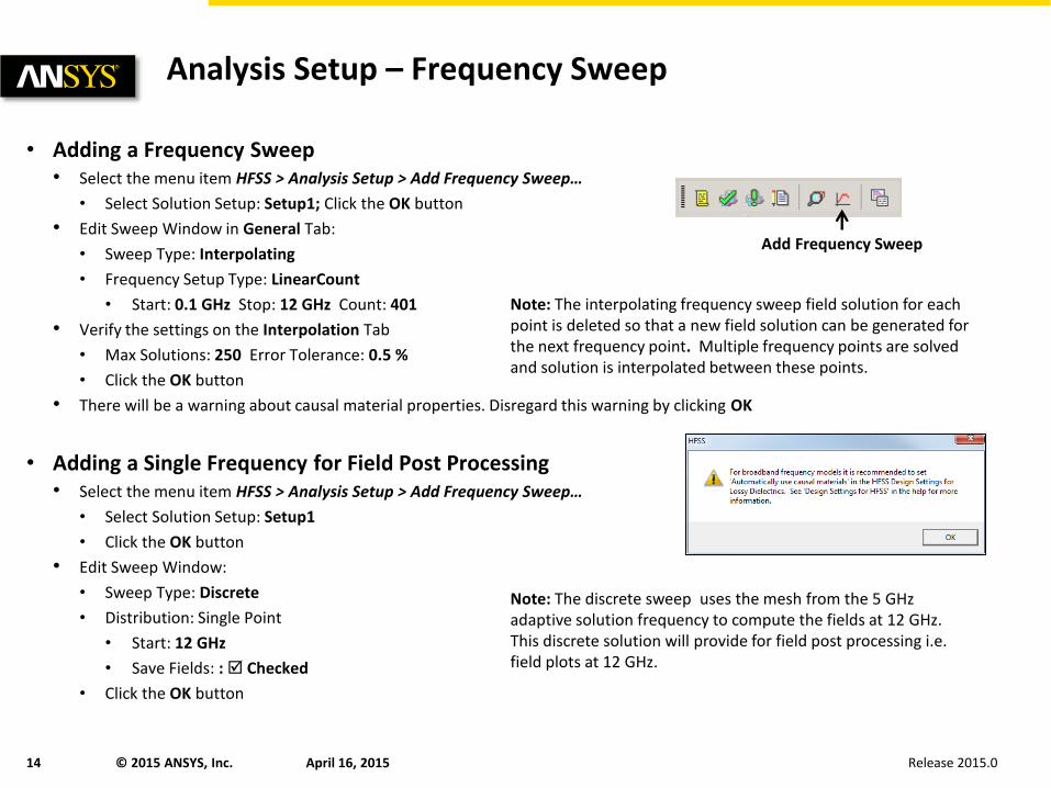
Analysis Setup – Frequency Sweep
• Adding a Frequency Sweep • Select the menu item HFSS > Analysis Setup > Add Frequency Sweep…
• Select Solution Setup: Setup1; Click the OK button
• Edit Sweep Window in General Tab:
• Sweep Type: Interpolating
• Frequency Setup Type: LinearCount
• Start: 0.1 GHz Stop: 12 GHz Count: 401
• Verify the settings on the Interpolation Tab
• Max Solutions: 250 Error Tolerance: 0.5 %
• Click the OK button
• There will be a warning about causal material properties. Disregard this warning by clicking OK
• Adding a Single Frequency for Field Post Processing • Select the menu item HFSS > Analysis Setup > Add Frequency Sweep…
• Select Solution Setup: Setup1
• Click the OK button
• Edit Sweep Window:
• Sweep Type: Discrete
• Distribution: Single Point
• Start: 12 GHz
• Save Fields: : Checked
• Click the OK button
Add Frequency Sweep
Note: The interpolating frequency sweep field solution for each point is deleted so that a new field solution can be generated for the next frequency point. Multiple frequency points are solved and solution is interpolated between these points.
Note: The discrete sweep uses the mesh from the 5 GHz adaptive solution frequency to compute the fields at 12 GHz. This discrete solution will provide for field post processing i.e. field plots at 12 GHz.
Release 2015.0 April 16, 2015 15 © 2015 ANSYS, Inc.
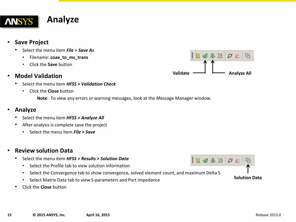
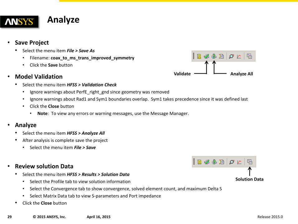
Analyze
• Save Project • Select the menu item File > Save As
• Filename: coax_to_ms_trans
• Click the Save button
• Model Validation • Select the menu item HFSS > Validation Check
• Click the Close button
Note: To view any errors or warning messages, look at the Message Manager window.
• Analyze • Select the menu item HFSS > Analyze All
• After analysis is complete save the project
• Select the menu item File > Save
• Review solution Data • Select the menu item HFSS > Results > Solution Data
• Select the Profile tab to view solution information
• Select the Convergence tab to show convergence, solved element count, and maximum Delta S
• Select Matrix Data tab to view S-parameters and Port impedance
• Click the Close button
Validate Analyze All
Solution Data
Release 2015.0 April 16, 2015 16 © 2015 ANSYS, Inc.
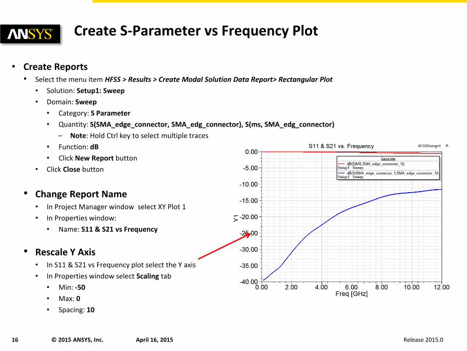
Create S-Parameter vs Frequency Plot
• Create Reports • Select the menu item HFSS > Results > Create Modal Solution Data Report> Rectangular Plot
• Solution: Setup1: Sweep
• Domain: Sweep
• Category: S Parameter
• Quantity: S(SMA_edge_connector, SMA_edg_connector), S(ms, SMA_edg_connector)
– Note: Hold Ctrl key to select multiple traces
• Function: dB
• Click New Report button
• Click Close button
• Change Report Name • In Project Manager window select XY Plot 1
• In Properties window:
• Name: S11 & S21 vs Frequency
• Rescale Y Axis • In S11 & S21 vs Frequency plot select the Y axis
• In Properties window select Scaling tab
• Min: -50
• Max: 0
• Spacing: 10
Release 2015.0 April 16, 2015 17 © 2015 ANSYS, Inc.
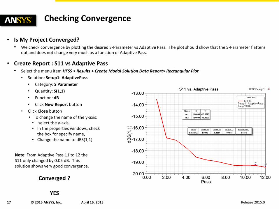
Checking Convergence
• Is My Project Converged? • We check convergence by plotting the desired S-Parameter vs Adaptive Pass. The plot should show that the S-Parameter flattens
out and does not change very much as a function of Adaptive Pass.
• Create Report : S11 vs Adaptive Pass • Select the menu item HFSS > Results > Create Modal Solution Data Report> Rectangular Plot
• Solution: Setup1: AdaptivePass
• Category: S Parameter
• Quantity: S(1,1)
• Function: dB
• Click New Report button
• Click Close button
Note: From Adaptive Pass 11 to 12 the S11 only changed by 0.05 dB. This solution shows very good convergence.
Converged ?
YES
• To change the name of the y-axis: • select the y-axis, • In the properties windows, check
the box for specify name, • Change the name to dBS(1,1)
Release 2015.0 April 16, 2015 18 © 2015 ANSYS, Inc.
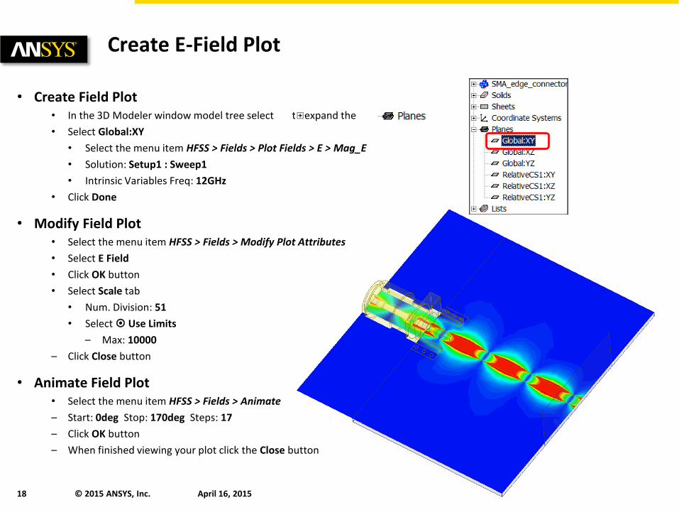
Create E-Field Plot
• Create Field Plot • In the 3D Modeler window model tree select to expand the
• Select Global:XY
• Select the menu item HFSS > Fields > Plot Fields > E > Mag_E
• Solution: Setup1 : Sweep1
• Intrinsic Variables Freq: 12GHz
• Click Done
• Modify Field Plot • Select the menu item HFSS > Fields > Modify Plot Attributes
• Select E Field
• Click OK button
• Select Scale tab
• Num. Division: 51
• Select Use Limits
– Max: 10000
– Click Close button
• Animate Field Plot • Select the menu item HFSS > Fields > Animate
– Start: 0deg Stop: 170deg Steps: 17
– Click OK button
– When finished viewing your plot click the Close button
Release 2015.0 April 16, 2015 19 © 2015 ANSYS, Inc.
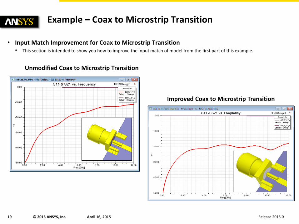
Example – Coax to Microstrip Transition
• Input Match Improvement for Coax to Microstrip Transition • This section is intended to show you how to improve the input match of model from the first part of this example.
Unmodified Coax to Microstrip Transition
Improved Coax to Microstrip Transition
Release 2015.0 April 16, 2015 20 © 2015 ANSYS, Inc.
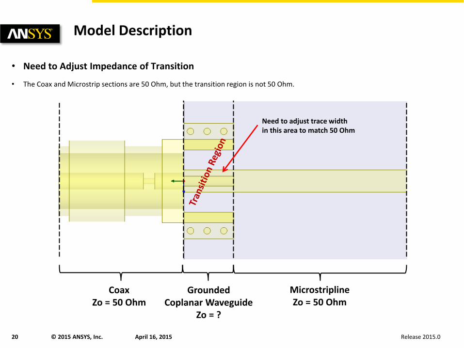
Model Description
• Need to Adjust Impedance of Transition
• The Coax and Microstrip sections are 50 Ohm, but the transition region is not 50 Ohm.
Grounded Coplanar Waveguide
Zo = ?
Microstripline Zo = 50 Ohm
Coax Zo = 50 Ohm
Need to adjust trace width in this area to match 50 Ohm
Release 2015.0 April 16, 2015 21 © 2015 ANSYS, Inc.
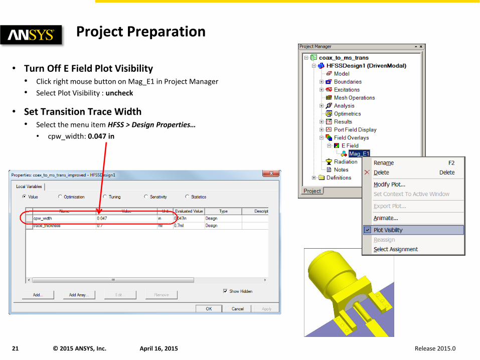
Project Preparation
• Turn Off E Field Plot Visibility • Click right mouse button on Mag_E1 in Project Manager
• Select Plot Visibility : uncheck
• Set Transition Trace Width • Select the menu item HFSS > Design Properties…
• cpw_width: 0.047 in

Release 2015.0 April 16, 2015 22 © 2015 ANSYS, Inc.
Analyze
• Save Project • Select the menu item File > Save As
• Filename: coax_to_ms_trans_improved
• Click the Save button
• Model Validation • Select the menu item HFSS > Validation Check
• Click the Close button
• Note: To view any errors or warning messages, use the Message Manager.
• Analyze • Select the menu item HFSS > Analyze All
• After analysis is complete save the project
• Select the menu item File > Save
• Review solution Data • Select the menu item HFSS > Results > Solution Data
• Select the Profile tab to view solution information
• Select the Convergence tab to show convergence, solved element count, and maximum Delta S
• Select Matrix Data tab to view S-parameters and Port impedance
• Click the Close button
Solution Data
Validate Analyze All
Release 2015.0 April 16, 2015 23 © 2015 ANSYS, Inc.
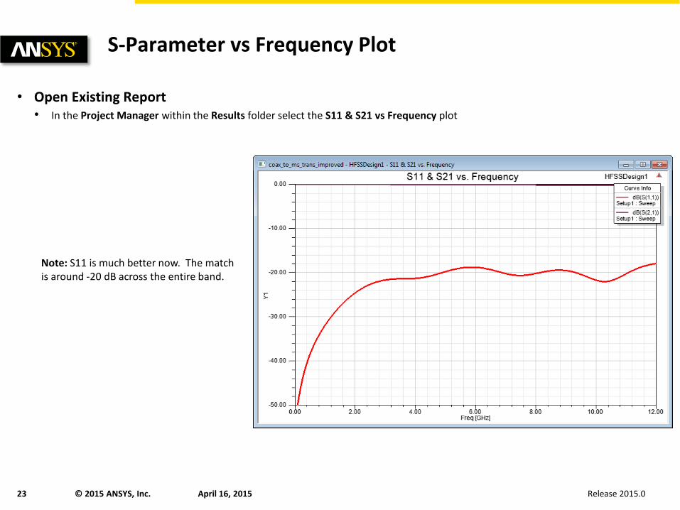
S-Parameter vs Frequency Plot
• Open Existing Report • In the Project Manager within the Results folder select the S11 & S21 vs Frequency plot
Note: S11 is much better now. The match is around -20 dB across the entire band.
Release 2015.0 April 16, 2015 24 © 2015 ANSYS, Inc.
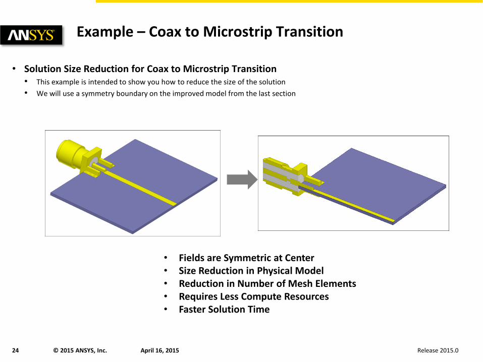
Example – Coax to Microstrip Transition
• Solution Size Reduction for Coax to Microstrip Transition • This example is intended to show you how to reduce the size of the solution
• We will use a symmetry boundary on the improved model from the last section
• Fields are Symmetric at Center • Size Reduction in Physical Model • Reduction in Number of Mesh Elements • Requires Less Compute Resources • Faster Solution Time
Release 2015.0 April 16, 2015 25 © 2015 ANSYS, Inc.
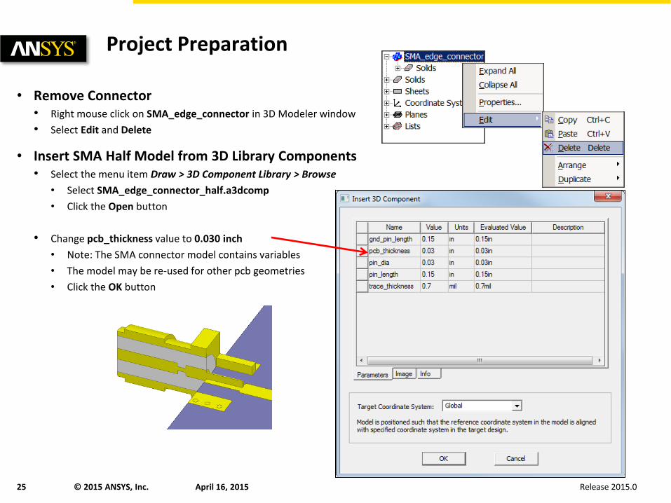
Project Preparation
• Remove Connector • Right mouse click on SMA_edge_connector in 3D Modeler window
• Select Edit and Delete
• Insert SMA Half Model from 3D Library Components • Select the menu item Draw > 3D Component Library > Browse
• Select SMA_edge_connector_half.a3dcomp
• Click the Open button
• Change pcb_thickness value to 0.030 inch
• Note: The SMA connector model contains variables
• The model may be re-used for other pcb geometries
• Click the OK button
Release 2015.0 April 16, 2015 26 © 2015 ANSYS, Inc.
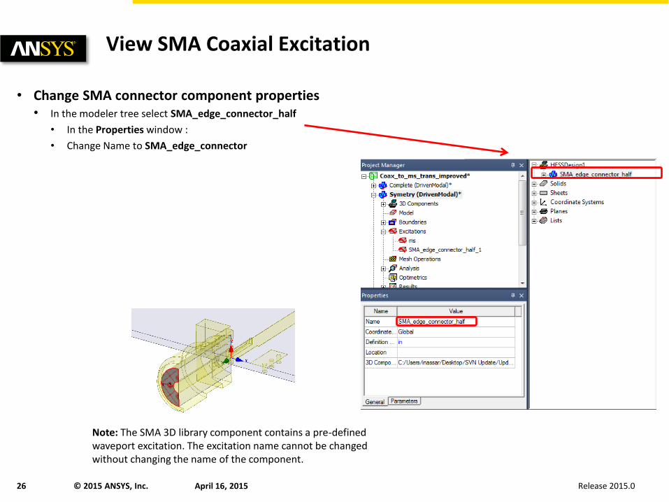
View SMA Coaxial Excitation
• Change SMA connector component properties • In the modeler tree select SMA_edge_connector_half
• In the Properties window :
• Change Name to SMA_edge_connector
Note: The SMA 3D library component contains a pre-defined waveport excitation. The excitation name cannot be changed without changing the name of the component.
Release 2015.0 April 16, 2015 27 © 2015 ANSYS, Inc.
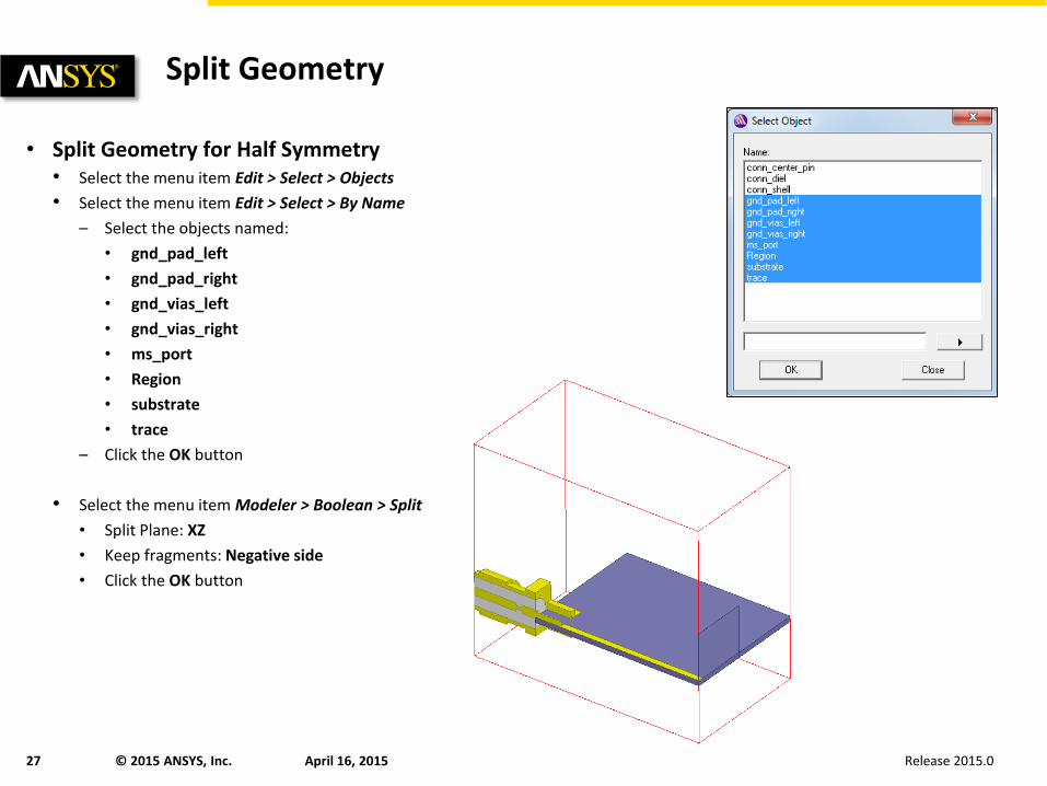
Split Geometry
• Split Geometry for Half Symmetry • Select the menu item Edit > Select > Objects
• Select the menu item Edit > Select > By Name
– Select the objects named:
• gnd_pad_left
• gnd_pad_right
• gnd_vias_left
• gnd_vias_right
• ms_port
• Region
• substrate
• trace
– Click the OK button
• Select the menu item Modeler > Boolean > Split
• Split Plane: XZ
• Keep fragments: Negative side
• Click the OK button
Release 2015.0 April 16, 2015 28 © 2015 ANSYS, Inc.
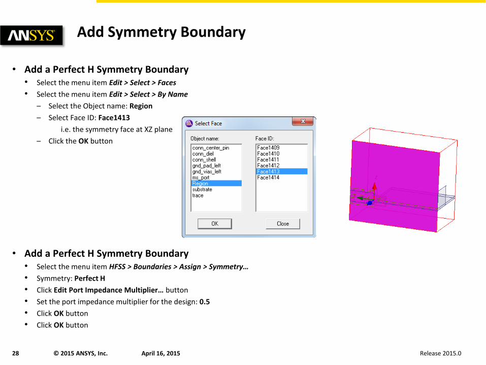
Add Symmetry Boundary
• Add a Perfect H Symmetry Boundary • Select the menu item Edit > Select > Faces
• Select the menu item Edit > Select > By Name
– Select the Object name: Region
– Select Face ID: Face1413
i.e. the symmetry face at XZ plane
– Click the OK button
• Add a Perfect H Symmetry Boundary • Select the menu item HFSS > Boundaries > Assign > Symmetry…
• Symmetry: Perfect H
• Click Edit Port Impedance Multiplier… button
• Set the port impedance multiplier for the design: 0.5
• Click OK button
• Click OK button
Release 2015.0 April 16, 2015 29 © 2015 ANSYS, Inc.
Analyze
• Save Project • Select the menu item File > Save As
• Filename: coax_to_ms_trans_improved_symmetry
• Click the Save button
• Model Validation • Select the menu item HFSS > Validation Check
• Ignore warnings about PerfE_right_gnd since geometry was removed
• Ignore warnings about Rad1 and Sym1 boundaries overlap. Sym1 takes precedence since it was defined last
• Click the Close button
• Note: To view any errors or warning messages, use the Message Manager.
• Analyze • Select the menu item HFSS > Analyze All
• After analysis is complete save the project
• Select the menu item File > Save
• Review solution Data • Select the menu item HFSS > Results > Solution Data
• Select the Profile tab to view solution information
• Select the Convergence tab to show convergence, solved element count, and maximum Delta S
• Select Matrix Data tab to view S-parameters and Port impedance
• Click the Close button
Solution Data
Validate Analyze All
Release 2015.0 April 16, 2015 30 © 2015 ANSYS, Inc.
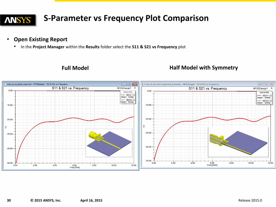
S-Parameter vs Frequency Plot Comparison
• Open Existing Report • In the Project Manager within the Results folder select the S11 & S21 vs Frequency plot
Half Model with Symmetry Full Model
Release 2015.0 April 16, 2015 31 © 2015 ANSYS, Inc.
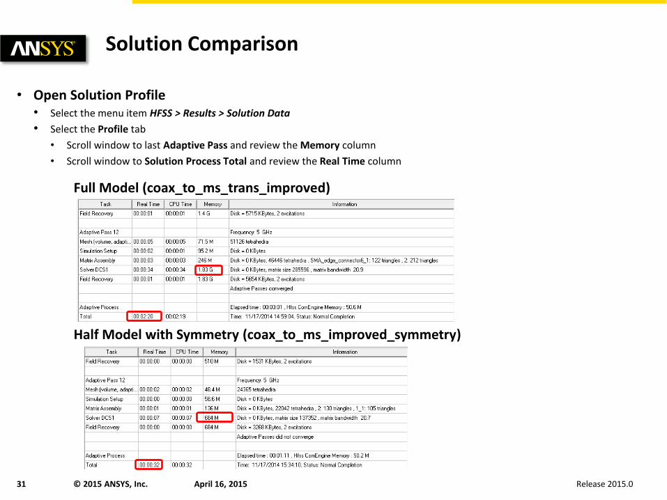
Solution Comparison
• Open Solution Profile • Select the menu item HFSS > Results > Solution Data
• Select the Profile tab
• Scroll window to last Adaptive Pass and review the Memory column
• Scroll window to Solution Process Total and review the Real Time column
Half Model with Symmetry (coax_to_ms_improved_symmetry)
Full Model (coax_to_ms_trans_improved)

Release 2015.0 April 16, 2015 32 © 2015 ANSYS, Inc.
This page intentionally left blank


![qudev.phys.ethz.ch · (b) 500nm 100 m . Gate Charge, ng [e] 40 30 2 20 Gate Charge, ng [e] coax . coax coax coax coax coax . probe 2 serv Control probe I ate 1 Target microwave coupler](https://img.pdfslide.us/doc/110x75/5f07545e7e708231d41c725e/qudevphysethzch-b-500nm-100-m-gate-charge-ng-e-40-30-2-20-gate-charge.jpg)