Embed Size (px)
Citation preview

Warsaw University of TechnologyDepartment of Electronics and Information Technologies
Institute of Electronic Systems
Wojciech Jałmużna (index no 180896)Warsaw ELEHP Group and DESY LLRF Team
Thesis for Master of Science in Electronics Engineering
Design and implementation of universal mathematical library supporting
algorithm development for FPGA based systems in high energy physics
experiments
The work done under supervision ofprof. nzw. dr hab. Ryszard Romaniuk and dr Krzysztof Pozniak, in cooperation with dr Stefan Simrock
Warsaw, February 2006
1

Contents
I. Abstract......................................................................................................................3II. Abstract in Polish ................................................................................................... 41. Introduction...............................................................................................................7
1.1 Control algorithm............................................................................................. 101.2 Modern solutions..............................................................................................121.3 FPGA based controller ( SIMCON )................................................................151.4 Algorithm development................................................................................... 20
2.System reqirements..................................................................................................233.Concept of a synchronous mathematical library for FPGA chips........................... 24
3.1 math_basic_signed and math_basic_unsigned modules.................................. 263.2 math_complex module..................................................................................... 273.3 math_matrix module........................................................................................ 283.4 IQ estimator......................................................................................................293.5 CORDIC stage................................................................................................. 303.6 Magnitude and Phase detector..........................................................................313.7 Sin/Cos calculation...........................................................................................323.8 SRT stage......................................................................................................... 343.9 Fixed point divider........................................................................................... 373.10 Floating point unit.......................................................................................... 373.11 OPB wrapper..................................................................................................383.12 Summary........................................................................................................ 38
4. Implementation....................................................................................................... 404.1 math_basic_unsigned....................................................................................... 404.2 math_basic_signed........................................................................................... 424.3 math_complex.................................................................................................. 444.4 math_matrix..................................................................................................... 454.5 IQ demodulator................................................................................................ 474.6 CORDIC...........................................................................................................484.7 SRT.................................................................................................................. 514.8 Floating point unit............................................................................................ 534.9 FIR filter...........................................................................................................554.10 OPB wrapper..................................................................................................574.11 Summary........................................................................................................ 58
5.Tests of designed system......................................................................................... 595.1 Cavity detuning measurment – algorithm and implementation....................... 615.2 Floating point unit tests....................................................................................725.3 Matrix multiplication tests............................................................................... 73
6.Summary and conclusions....................................................................................... 75References...................................................................................................................77Acknowledgments.......................................................................................................797.Appendixes.............................................................................................................. 80
2

I. Abstract
The X-ray free-electron laser XFEL that is being planned at the DESY research
center in cooperation with European partners will produce high-intensity ultra-short X-
ray flashes with the properties of laser light. This new light source, which can only be
described in terms of superlatives, will open up a whole range of new perspectives for
the natural sciences. It could also offer very promising opportunities for industrial users.
SIMCON (SIMulator and CONtroller) is the project of the fast, low latency
digital controller dedicated for LLRF system in VUV FEL experiment based on modern
FPGA chips It is being developed by ELHEP group in Institute of Electronic Systems
at Warsaw University of Technology. The main purpose of the project is to create a
controller for stabilizing the vector sum of fields in cavities of one cryomodule in the
experiment. The device can be also used as the simulator of the cavity and testbench for
other devices. Flexibility and computation power of this device allow implementation of
fast mathematical algorithms.
This paper describes the concept, implementation and tests of universal
mathematical library for FPGA algorithm implemetation. It consists of many useful
components such as IQ demodulator, division block, library for complex and floating
point operations, etc. It is able to speed up implementation time of many complicated
algorithms. Library have already been tested using real accelerator signals and the
performance achieved is satisfactory.
3
II. Abstract in Polish
Projekt XFEL, który planowany jest w instytucie badawczym DESY w
Hamburgu będzie w stanie dostarczyć krótkie impulsy promieniowania X o wysokim
natężeniu z właściwościami światła laserowego. Jego świetlność moży być nawet
milion razy większa od najbardziej nowoczesnych źródeł promieniowania X.
Międzynarodowa grupa badawcza o nazwie 'TESLA collaboration' testuje obecnie
nowatorski technologie w ośrodku DESY. Osiągnęła ona już wiele z kluczowych celów
postawionych przed nimi. XFEL umożliwi wykonywanie zaawansowanych badań w
Europie. Stworzy również wiele mozliwości dla ośrodkó przemysłowych. Pilotowym
odcinkiem dla XFEL jest akcelerator VUV-FEL, w którym odbywaja się testy.
Jedną z nowatorskich technologi wporowadzonych w użycie przy VUV-FELu są
programowalne układy FPGA. W ciągu ostatnich lat zaobserwowano szybki rozwój na
tym rynku. Obecnie moc obliczeniowa tych układów może być porównana z mocą
obliczeniową procesorów DSP. Ponadto architektura tych chipów jest otwarta – może
być optymalizowana razem z algorytmem matematycznym. Wiele układów FPGA ma
możliwość użycia procesorów osadzonych takich jak PowerPC, Nios, Microblaze.
Programy pisane na te procesory mogą zostać połączone ze sprzętowymi blokami
rownoległego przetwarzania sygnału.
W chwili obecnej w użyciu znajduje się oparty na ukłądzie FPGA kontroler
opracowany przez grupę ELHEP. Jest to kolejna generacja płyty z rodziny SIMCON.
Bazuje ona na chipie FPGA XC2VP30 firmy Xilinx. Bogate peryferia oferują duże
możliwości komunikacyjno-obliczeniowe. Może ona stać się bazą wielu implementacji
algorytmów matematycznych.
Szybki rozwój możliwości technicznych pociąga za sobą rozwój algorytmów
matematycznych. Ich implementacja przy użyciu języka opisu sprzętu ( VHDL ) staje
się skomplikowana i czasochłonna. Rośnie czas dostarczenia gotowego produktu. Na
wprost tego wychodzą producenci oprogramowania używanego do implementacji.
Interfejsy tych programów są coraz bardziej uproszczane. Oferują one graficzne
narzędzia do tworzenia opisów sprzętu. Przyspiesza to znacznie proces implementacji.
4

Pociąga za soba równiez jedną wade – maleje kontrola nad szczegółami implementacji
w sprzęcie. Praca ta prezentuje inne z możliwych rozwiązań tego problemu. Jej celem
jest stworzenie koncepcji oraz implementacja uniwersalnej i parametrycznej biblioteki
matematycznej wspierającej implementację i rozwój algorytmów matematycznych w
układach FPGA.
Biblioteka została podzielona na następujące części:
– moduły wejściowe
w skład tej grupty wchodzą moduły takie jak demodulator IQ oraz blok obliczający
amplitude i faze liczby zespolonej. Użyte mogą zostać do wstępnej konwersji
sygnału z akceleratora do wymaganej reprezentacji. Dostarczają one sygnał do
komponentów z kolejnej grupy.
– moduły obliczeniowe
są to główne moduły wykonujące konkretne obliczenia matematyczne. W ich skład
wchodzą bloki takie jak: dzielenie stalo pozycyjne, obliczanie funkcji
trygonometrycznych, operatory operacji na liczbach zespolonych, macierzowe
operacje arytmetyczne,regulowane filtry oraz jednostka do obliczen zmienno
pozycyjnych.
– wsparcie dla systemów osadzonych
w tej grupie znajduje sie moduł 'OPB wrapper' mapujący zbiór rejestrów
zdefiniowanych w strukturze FPGA w przestrzeń adresową systemu osadzonego.
Umożliwia to miesznae podjeście do implementacji algorytmów – mniej krytyczne
częsci mogą zostać zaimplementowane w języku wyższego poziomu ( na przykład
C ) i komunikować sie z krytycznymi sekcjami obliczanymi przez sprzęt. Moduł ten
umożliwia również dołączenie wymienionej wyżej jednostki zmiennopozycyjnej
jako koprocesora dla PowerPC.
– moduły niskopoziomowe
5

są to biblioteki podstawowe użyte do zaimplementowania pozostałych modułów.
Udostępnione są one uzytkownikowi, aby mógł użyć je w przypadku kiedy
wymagana jest funkcjonalność nieuwzględniona w bibliotece. Implementują one
podstawowe koncepty operacji arytmetycznych takie jak arytmetyga nasycona,
operatory arytmetyczne dla macierzy, liczb zespolonych, liczb
zmiennopozycyjnych.
Architektura bibliotek jest otwarta. Dzięki temu istnieje wiele możliwości
dodawania nowych komponentów i ulepszania starych. Nowe komponenty mogą zostać
dodane do biblioteki nawet przez zwykłych użytkowników. Wszystkie bloki zostały
zoptymalizowane aby zapewnic rozsądny wybór między użytymi zasobami a
szybkością działania. Jednak w miarę rozwoju rynku FPGA – rosnących możliwości
technicznych – konieczne będzie dostosowywanie biblioteki do zmieniających sie
warunków.
Wszystkie użyte w niej algorytmy obliczeniowe są algorytmami dobrze znanymi
w przetwarzaniu DSP. Przykładem może być tu algorytm demodulacji IQ używany
obecnie w kontrolerze FPGA dla moduły ACC1 akceleratora VUV-FEL lub algorytm
dzielenia SRT uzywany w procesorach firmy Intel.
Szczegóły implementacji – interfejsy i parametry - poszczególnych modułów
pokazane zostały w rozdziale 4 tej pracy.
Rozdział 5 przedstawia testy biblioteki w środowisku akceleratorowym. W tym
celu zaimplementowany został algorytm matematyczny pomiaru odstrojenia wneki
rezonansowej podczas pojedynczego pulsu pola elektromagnetycznego wewnątrz
wneki. Uzyskana implementacje spełnia wszystkie oczekiwania – wejdzie ona w skład
planowanego systemu kontroli. Przetestowany został również blok operacji
zmiennopozycyjnych. Przyspieszenie obliczeń procesora osadzonego w porównaniu z
emulacją programową wynosi około 1000%. Rezultaty uzyskane dla mnożenia
macierzy 20 na 20 elementów również są bardzo ciekawe. Czas wykonania takiego
mnożenia wynosi około 80 us.
Przedstawiona biblioteka spełnia wszystkie wymagania postawione przez system
sterowania LLRF i ma szanse stać sie popularnym narzędziem implementacji
algorytmów matematycznych.
6

1. Introduction
The X-Ray Free-Electron Laser, which is planned at the DESY research center
[15] will produce high-intensity ultra-short X-ray pulses with the properties of laser
light. At peak values, its brilliance is a billion times higher than that of the most modern
X-ray light sources, and its average brilliance is 10 000 times higher. An international
research team, the TESLA collaboration, is currently demonstrating the facility's
pioneering technology at the DESY research center in Hamburg. It has already achieved
the key milestones it has been aiming for. The free-electron X-ray laser will make it
possible to do leading-edge research in Europe and will also offer very promising
opportunities for industrial users
The layout of the accelerator and laser facility is shown on Figure 1.
7
Figure 1: X-FEL facility layout

Main parameters of XFEL facility are [15]:
Total length of the facility approx. 3.4 km Accelerator tunnel approx. 2.1 km Depth underground 6 - 38 m Experimental hall 10 experimental stations at 5 beamlines, Scope for expansion Second hall with an 10 experimental stations Wavelength of X-ray radiation 6 to 0.085 nanometers (nm) Length of radiation pulses below 100 femtoseconds (fs)
Table 1: X-FEL main parameters
The planned facility will include a superconducting linear accelerator that brings
tightly bundled “bunches” of electrons to energies of several billion electron volts. At
that point, the electrons race at almost the speed of light along a slalom course through a
special arrangement of magnets called the “undulator.” As they go, they emit X-ray
radiation that amplifies itself during the flight. The results are brilliant: Extremely short
and intense X-ray flashes with laser properties. For such an X-ray laser to work, an
electron beam of extremely high quality is required. And the TESLA superconducting
accelerator technology is already making it possible to generate this kind of electron
beam today.
Before the electrons can emit X-ray flashes, they must first be accelerated to
energies of several billion electronvolts. That's exactly what happens inside the
resonators, where electromagnetic fields accelerate the particles. The resonators are
made of niobium and are superconducting: When they are cooled to a temperature of
-271 °C, they loose their electrical resistance. Electrical current then flows through the
resonators with almost no losses whatsoever - and that's an extremely efficient and
energy-saving method of acceleration. Nearly the entire rf power is transferred to the
particles. Moreover, the superconducting resonators deliver an extraordinarily fine and
even electron beam of extremely high quality. In the X-ray laser, each of several billion
electrons needs to have the same energy and direction. They also need to be combined
into bunches with a diameter of no more than one tenth of a millimeter to achieve the
necessary peak current of 5kA. Unless the electron beam meets these very special
8

requirements, the X-ray laser does not work.
The new free-electron laser VUV-FEL - the pilot facility for the XFEL - , which
generates vacuum ultraviolet (VUV) and soft X-ray radiation in a range down to
wavelengths of six nanometers, was commissioned in 2004, making possible
groundbreaking experiments. To accommodate the new free-electron laser, the 100-
meter-long TESLA test facility was modified to a total length of 260 meters and
extended to the VUV-FEL. Both VUV-FEL and XFEL are based on the same
superconducting technology.
In the VUV-FEL cavities are grouped into cryomodules which contain 8 cavities
each. The cavities are powered by klystrons ( 32 per klystron ). In order to get
appropriate beam acceleration two conditions must be met:
1. the electromagnetic field inside resonators must be stabilized ( to ensure stable
beam energy )
2. it must have appropriate phase ( for bunch compression and acceleration )
The regulation of the field is performed by the LLRF – Low Level Radio
Frequency control system. It controls I and Q components of resonator field. They
correspond to real and imaginary part of the field vector. The control section, powered
by one klystron, may consist of many cavities, so the LLRF system is used to control
vector sum of up to 32 cavity fields. The system consists of many devices such as:
downconverters, digital feedback controllers,vector modulators, piezo controllers,
timing modules, and many ADC boards for monitoring the signals in the system.
9
Figure 2: VUV-FEL structure schematic

1.1 Control algorithm
The main control loop in the LLRF system starts at the cavity probe. The signals
(1.3GHz) are downconverted to an intermediate frequency of 250KHz. Eight
downconverted signals are connected to inputs of digital controller. It samples the
probe signal with a frequency of 1MHz. Inside the controller (currently it is a DSP
based system) after initial calibration (scaling and leveling), the digital processing is
performed in I/Q detector applying the signal v_m of the intermediate frequency at 250
kHz. The resultant cavity voltage envelope (I, Q) is calibrated, so to compensate the
phase offset for an individual measurement channel. The vector sum of up to 32 signals
is needed for the actual control processing. Feedforward and Feedback algorithms can
be used to control the system.
The Set-Point table delivers the required signal level, which is compared to the
actual average value of the cavities voltage envelope. Then the proportional controller
amplifies the signal error according to data from the GAIN table and closes the
feedback loop. Additionally the Feed-Forward Table is applied to improve
compensation of the repetitive perturbations induced by the beam loading and by the
dynamic Lorentz force detuning. I and Q signals are produced to drive the klystron.
These two signals are used by the vector modulator to reconstruct the complex signal.
The output of this vector modulator drives the klystron. When using 1MHz sampling
rate, the probe samples are updated every 1μs. High gain must be used to stabilize the
field using feedback algorithm. This may cause unstability in the system if the feedback
latency is to high. The maximum latency for the feedback algorithm has been estimated
to about 1μs (for the whole control loop including latency of system and controller
board). The estimated system delay is about 500ns. It means that maximum delay of the
controller can not exceed 500ns. The requirements for the stability of the amplitude and
phase of the field are tight: for the amplitude 3*10−4 and for the phase 0.1 degree. The
main problem is noise which comes from microphonics, Lorentz force detuning and
beam loading. In addition lots of elements in the control loop are nonlinear, for example
klystron, vector modulator or preamplifiers. Every conversion from analog to digital
signal adds noise to the system. Moreover the temperature changes cause phase drifts in
10

cables. All these distortion are added to the control signal and force the controller to
compensate using sophisticated algorithms. This requires a big computation power of
the controller and wide data throughput.
11
Figure 3: Control system schematic

The current solution is based on the system with DSP processor (TMS320C67
from Texs Instruments). The controller is divided into three boards - ADC board with
14-bit analog to digital converters sampling with a frequency of 1MHz, the DSP board
with TMS320C67 processors and DAC board (14 bit, 1MHz). All the boards are
connected to each other using gigalink interface. Actual computation power is close to
the limit, the algorithm is performed in a time longer than 1μs. Moreover, during last
months there are additional needs for some new features. The only way to extend
current system with new features is to add more DSP processors. This solution requires
integration of new DSP board into existing system. It may cause some additional
problems and delays in machine operations.
To increase computation power and the delay of LLRF control system, both the
algorithm and hardware must be optimized. Unfortunately DSP processors have fixed
architecture so only the software can be processed. This will not grant the flexibility
required for further system developement.
1.2 Modern solutions
During past years very fast progress on the FPGA market was observed.
Nowadays FPGA chips have reached computation power that can be compared with
DSP processors. Moreover the architecture of those chips is not fixed. Just like software
algorithm it can be optimized to achieve optimal speed or resources usage ( depends on
requirements ). FPGA chips offer variety of the embedded solutions such as PowerPC,
Microblaze, Nios which can be easily used in addition to fast, parallel signal
processing.
Typical low level architecture of FPGA chip is shown on Figure 4
It consists of an array of logic blocks and routing channels. Multiple I/O pads
may fit into the height of one row or the width of one column. Generally, all the routing
channels have the same width. A logic block consists of a LookUp Table with 4 inputs
and a FlipFlop as shown on Figure 5.
12

In the modern solutions there are many functional blocks embedded into the
chip's architecture. These functional blocks are:
– RAM memory which can be used in data acquisition process
13
Figure 4: Low level architecture of FPGA chip
Figure 5: Logic block structure
4 input LUTD Flip Flop
output
clock
inputs

– dedicated DSP blocks for arithmetic operations
– digital clock managers ( PLLs ) for clock conversions
– Gigabit serializers that can connected to optical transcievers
– embedded processors which can run higher level software
Usage of these block simplifies the structure required for the algorithms, reduces
delays and increases computation power. Moreover each of these blocks can be used in
parallel.
The block RAM memory resources embedded into Xilinx FPGA [17] chips such
as Virtex 2 are 18 Kb of true Dual-Port RAM, programmable from 16K x 1 bit to 512 x
36 bit, in various depth and width configurations. Each port is totally synchronous and
independent, offering three "read-during-write" modes. Block RAM memory is
cascadable to implement large embedded storage blocks. Supported memory
configurations for dual-port and single-port modes are shown in Table 2.
16K x 1 bit 4K x 4 bits 1K x 18 bits8K x 2 bits 2K x 9 bits 512 x 36 bits
Table 2: internal memory configurations
A multiplier block is associated with each RAM memory block. The multiplier
block is a dedicated 18 x 18-bit 2s complement signed multiplier, and is optimized for
operations based on the block RAM content on one port. The 18 x 18 multiplier can be
used independently of the block RAM resource. Read/multiply/accumulate operations
and DSP filter structures are extremely efficient.
Both the RAM memory and the multiplier resource are connected to four switch
matrices to access the general routing resources.
Processors embedded into FPGA chips have become very popular during past
years. The main vendors of embedded solutions are Altera and Xilinx companies
[17,18]. Altera introduced Nios and Nios II soft processor core which is built using user
logic during configuration process. The similar solution comes from Xilinx company
and is called Microblaze. Both companies made a big effort to optimize their cores to
achieve high performance. These cores can easily be integrated with other user logic
14

and peripherials, therefore the hardware implementation of an algorithm can be
supported by calculations described in higher level programming language such as C or
C++.
The most important and unique embedded solution was introduced by Xilinx
company. It is PowerPC 405 hardware core placed directly into silicon structure of
FPGA chip. The main advantages of such approach are:
– user logic can be completely independent from processor
– it uses minimal number of FPGA resources
– it offers superior performance in comparison with soft cores
The most known FPGA vendors are Altera and Xilinx companies. Comparison
of different chips is shown in Table 3.
FPGAchip
Logic cells RAM Hardware multipliers
gigalinks PowerPCs Max user IO
XC2V3000 32,256 1,728 96 0 0 720XC2V400 51,840 2,160 120 0 0 912XC2VP30 30,816 2,448 136 8 2 644XC2VP50 53,136 4,176 232 16 2 852EP1S30 32,470 3,317 96 0 0 726
EP1SGX40 41,250 3,423 112 20 0 624
Table 3: parameters of Xilinx and Altera chips
Although DSP processors are more flexible for complex algorithms, the
structural flexibility of FPGA chips together with parallel calculations and integrated
peripherials make more powerful unit for general purpose and arithmetic operations.
LLRF control system based on FPGAs can be smaller, faster and more extensible than
DSP based one.
1.3 FPGA based controller ( SIMCON )
SIMCON (SIMulator and CONtroller) [2,5] is the project of the fast, low latency
15

digital controller dedicated for LLRF system in VUV FEL experiment It is being
developed by ELHEP group in Institute of Electronic Systems at Warsaw University of
Technology. The purpose of the project is to create a controller that can stabilize the
vector sum of fields in resonators driven by one klystron and gather experience and
knowledge for future XFEL control system development. It can also be also used as the
simulator of the cavity, test bench for other devices and algorithm development studio.
SIMCON design is based on FPGA technology. It allows to create fast hardware
devices inside the chip, each dedicated for the particular purpose. Therefore it is faster
than currently used controller based on DSP processors. Moreover the flexibility of
FPGA chips allows to extend existing controllers with new features without any
changes in current implementation and architecture of the PCBs. FPGA technology
offers integrated peripherals for the fast communication (optical links) and calculations
(embedded PPC or DSP blocks). All these features create powerful platform for control
system development. The flexibility of FPGA technology used in SIMCON makes this
device multipurpose system which can perform many sophisticated algorithms. Its
capabilities are limited by the board architecture which includes size of the FPGA chip
used. The basic structure of the SIMCON system is shown on Figure 6.
16
Figure 6: Structure of FPGA based controller
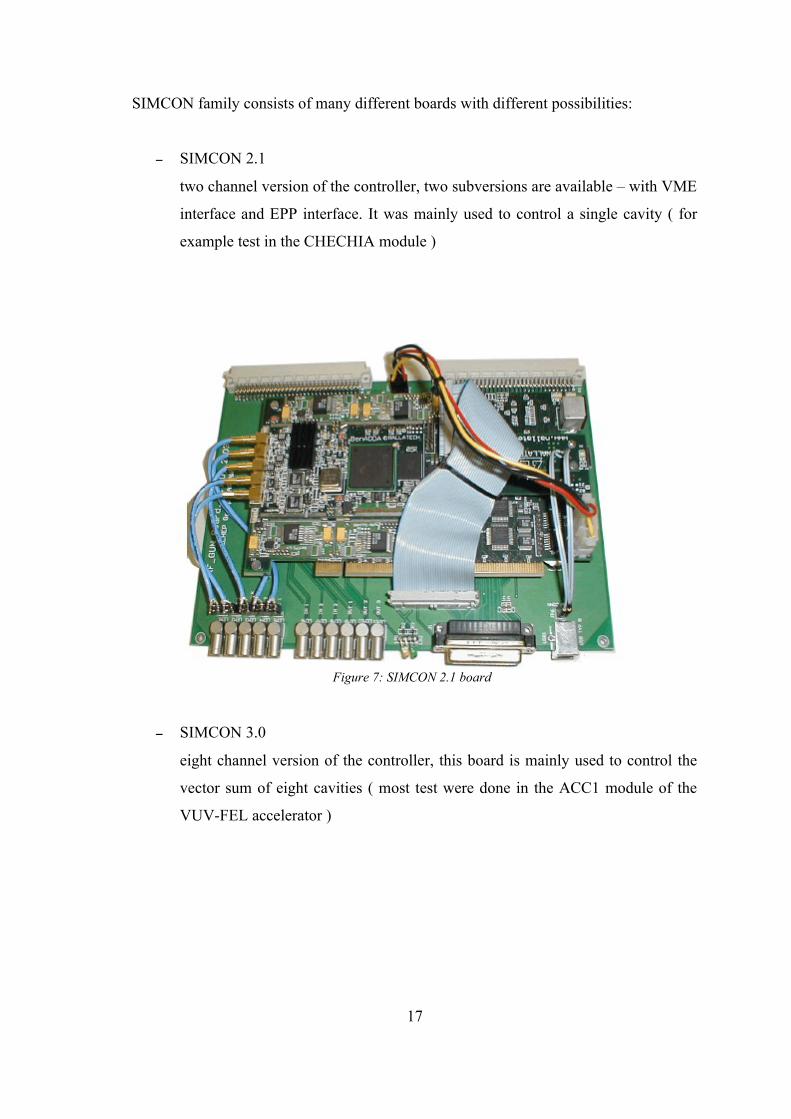
SIMCON family consists of many different boards with different possibilities:
– SIMCON 2.1
two channel version of the controller, two subversions are available – with VME
interface and EPP interface. It was mainly used to control a single cavity ( for
example test in the CHECHIA module )
– SIMCON 3.0
eight channel version of the controller, this board is mainly used to control the
vector sum of eight cavities ( most test were done in the ACC1 module of the
VUV-FEL accelerator )
17
Figure 7: SIMCON 2.1 board

The current version of SIMCON (3.1) was designed for controlling the vector
sum of fields in one cryo-module (8 cavities). The main features of the board are:
– Xilinx Virtex II Pro FPGA chip.
– Ten 14-bit ADCs (up to 105 Msps) and four 14-bit DACs (up to 160Msps).
– 2 inputs for external clock and trigger signals
– 2 outputs for providing the clock and trigger signal
– Additional digital inputs and outputs
– 16MB of SDRAM for embedded sytem use
– 8MB of SRAM for FPGA use
– Ethernet connector
– 2 Gigabit optical channels
– VME interface
18
Figure 8: SIMCON 3.0 board

Table 4 presents parameters of SIMCON boards.
Simcon 2.1 Simcon 3.0 Simcon 3.1FPGA chip Virtex II 3000 Virtex II 4000 Virtex 2 Pro 50ADC channels 1 8 10DAC channels 2 4 4Digital Outputs 2 2 2Digital Inputs 2 2 2Optical links - - 2PPC - - 2Interface EPP/VME VME/ETH/RS232 VME/ETH/RS232
Table 4: SIMCON family parameters
19
Figure 9: SIMCON 3.1 board

1.4 Algorithm development
Powerful FPGA platform such as the SIMCON 3.1 board opens a new
posibilities for algorithm development. In the DSP processor, the user has fixed
architecture and decides about its functionality and program flow using higher level
programming language. Therefore DSP is easier to program than FPGA chips.
Unfortunately it is only capable of serial processing with very limited parallel
possibilities. On the other hand FPGA chips are dedicated for parallel processing. In
FPGA, architecture of the chip must be described using hardware description language
such as VHDL ( Very-High-Speed Integrated Circuit Hardware Description Language ),
Verilog etc. User decides which calculations are going to be performed in parallel and
in serial, which functional blocks and peripherials to use. Program flow control is
achieved by defining state machines. Then, if neccesary, the user must integrate
described structure with embedded processor and create higher level software.
The described process is much more complicated than traditional DSP
programming and requires a lot of knowledge about binary operations, FPGA structure
and logical systems. Therefore algorithm development for FPGA chips may take much
more time than for DSP processors. To overcome this flaw different vendors of FPGA
chips and external companies have proposed many software solutions which enable
rapid algorithm development.
This software can be splited into following categories:
– schematic tools
– IP cores
Schematic tools allow programmer to describe even complicated system structures
using a simple graphical interface. The system is built using closed functional blocks
connected with each other. Then the VHDL code or netlist file is generated. Most
advanced schematic tools such as Xilinx System Generator offer high level
mathematical operations and integration with popular algorithm development software.
These tools give an easy way to describe functionality of the FPGA system, but it is
almost impossible to control the hardware architecture of the code. Nowadays, all the
design software provided by the manufacturers includes schematic tools for program
development.
20

The second category are IP cores. These are specialized functional block
prepared in a form of netlist or VHDL code which can be included and used in a user
program. Usage of IP cores gives an ability to describe the whole system using the
VHDL code without need to describe complicated mathematical operations etc. These
solution gives better control over FPGA resources and architecture. Unfortunately IP
cores are highly specialized and usually patented so there is practically no influence on
the interior of blocks – no user modification can be made therefore only small control
over their functionality is possible.
Both solutions can be combined – implemented algorithm may be the result of
using schematic tool together with VHDL programming and IP cores. Unfortunately
these solutions are quite expensive. Moreover LLRF control system requires some
functional blocks that are not commonly used, therefore they are not avaiable as IP
cores. An excellent example of a combined solution is the Xilinx Embedded
Development Kit which allows to build embedded system using a graphical schematic
21
Figure 10: Altera Quartus II schematic tool

tool to add IP cores as system's peripherals.
Algorithm development for the LLRF control system requires more flexibility
than one offered by described tools. Programming should be done using VHDL
language in addition with flexible IP cores and low level libraries developed for this
system. The source of the IP cores and libraries should be open to allow users to extend
them when needed or modify existing ones according to the needs.
22
Figure 11: Xilinx EDK for embedded systems

2. System reqirements
Fast development of electronic systems causes the parallel development of many
different mathematical algorithms. FPGAs possibilities are constantly expanding,
therefore the structural complexity of hardware is also rising. More work,time and skill
is required for algorithm implementation and usage. The aim of this thesis is:
- to design and implement universal mathematical library supporting algorithm
development for FPGA based systems in accelerator subsystem design
The main requirements for the project are:
1. the components must be synchronous – maximum working frequency is rising, it
is important to have extended control over all delays. It is hard to achieve in
asynchronous systems. Moreover it allows to synchronize many independent
channels ( for example 8 for SIMCON 3.1 ) and different components.
2. pipelining – it increases the maximum frequency and system bandwidth. The
signal samples can be gathered and processed without need to wait for the end of
the previous calculations. This speeds up algorithm execution time.
3. flexibility - components can work on many different boards with many FPGA
chips and variable channel number and can be modified to fit to particular user
needs.
4. choice between speed and resource usage - it allows to use components even
when hardware resources are critical, but speed is less important. This approach
causes that this library can be used in many offline measurement algorithms with
low resource usage
5. platform independence
6. support for popular VHDL synthesizers
7. easy to use
8. easy to maintain and change code
23

3. Concept of a synchronous mathematical library for FPGA chips
The concept of the library is based on the hierarchical tree of components. The
library must fulfill all the requirements for LLRF control system algorithm
development. Synchronous mathematical library allows easy latency control versus
hardware resources used. Each component is meant to be compatible with existing
solutions ( if available ). Moreover functional components are completely hermetical
and can be used separately ( providing that libraries in the same tree branch are
available), and most important, can be used in any combination of serial and parallel
connections.
Most signals from the accelerator modules come as vectors in IQ representation.
Therefore the first module in almost every algorithm for this sytsem will be IQ
demodulator which converts raw data sampled from ADC to a complex representation.
A good example is SIMCON controller algorithm in which the processing starts using
such block. This functional block should be included in this library to allow use in
other algorithms. After demodulation, the complex signals are calibrated ( scaled,
rotated ). It means that arithmetical operations on complex numbers are made. This task
is performed by the complex operation module. In some cases signals are filtered. That
is why the programmable digital finite impulse response filter was implemented. Both
modules can be used in the SIMCON algorithm and many others for rotation matrix
multiplication and signal filtering. In some algorithms it is neccesary to obtain
additional informations about the signal ( for example the magnitude of complex vector
or its phase – it was done in Cavity Detuning measurement algorithm ). For this reason
a module for magnitude and phase calculation has become part of this library. The
algorithm used in this module can be also used to calculate functions such as sine and
cosine when latency is not critical.
The only basic arithmetical operation without hardware support in FPGA is the
division. Lack of this operation can be major problem in some cases ( for example it is
needed in the Cavity Detuning measurement algorithm). Therefore division block is
24

included in this library.
To extend the flexibility of this library, in addition to fixed point arithmetics,
floating point units were added. This feature is valuable especially in connection with
embedded system development.
Moreover a special wrapper for the PowerPC embedded processor was added. It
allows to connect every component included in this library to Onboard Peripherial Bus
(OPB) [17]. This approch allows to combine the algorithm development process
between low level hardware description and higher level C programs executed on
embedded system.
The tree of components is shown on the Figure 12.
25
Figure 12: Structure of designed library
math_basicunsigned
math_complexMath_basicsigned
OPB wrapper
Fixed pointdivider
FLOATdivider
AP detector
SIN/COS calculation
FIRFilter
FLOATmultiplier
FLOATadder
SRTstage
CORDICstage
IQ demodulator
math_matrix

3.1 math_basic_signed and math_basic_unsigned modules
These modules provide basic functions for arithmetical operations used in other
modules. They are optimized to use dedicate hardware resources embedded into a
FPGA array such as hardware multipliers. Functions are meant to be easily used in user
applications – their interface is minimal.
The Math_basic_signed library provides functions that can operate on signed
values using two’s complement representation, which is the most popular and intuitive
method of representing negative integers. In the two's complement representation, the
most significant bit of a signed binary numeral indicates the sign. To obtain the absolute
value of the negative number, all the bits are inverted then 1 is added to the result. As
one can notice ‘0’ value has only one representation ( no negative ‘0’ and problems
associated with it ). Moreover all arithmetic operations are simple binary operations.
The library defines functions for number multiplication, addition and subtraction.
Moreover it allows to calculate absolute value and negation of a number. There are
functions that allow to resize a value to a specified number of bits and to shift it left or
right by specified number of bits. Each function has an intuitive interface and can be
easily used.
The Math_basic_unsigned library provides similar functions that can operate on
unsigned binary numbers. As signed library it defines functions for multiplication,
addition and subtraction of unsigned binary numbers. Functions for shifting and resizing
binary vectors are also included.
In the real time arithmetic operations, overflow is a big problem. When the big
values overflow, they suddenly become small or negative. It may lead the whole system
to undefined states. Such a situation is not allowed, it can be dangerous for the
accelerator and electronic hardware. Therefore, arithmetic operations in both libraries
use so called saturation arithmetic. Saturation arithmetic is a version of arithmetic in
which all operations such as addition and multiplication are limited to a fixed range
between a minimum and maximum value. If the result of an operation is above the
maximum it is set to the maximum, while if it is below the minimum it is set to the
minimum. In this case, the minimum and maximum values are defined by the length of
vectors used to represent numbers.
26

3.2 math_complex module
This module includes functions needed for complex number operations. It allows
to multiply, add and subtract complex numbers represented as real and imaginary parts.
Moreover it allows to calculate conjugation and rotate the number by 180 degrees.
When resizing complex number, both real and imaginary parts are resized to required
number of bits. The base for this module is math_signed library.
Arithmetic operations on complex number are more complicated than operations
on normal numbers. Addition ( or subtraction) of two numbers requires two additions of
signed values.
z1 = a+jb
z2 = c+jd
The result of an addition is
z1+z2 = (a+c) + j(b+d)
The result of a multiplication is
z1*z2 = (a*c - b*d) + j(a*d + b*c)
As one can see multiplication of two complex numbers uses six binary
operations ( 4 multiplications and 2 additions/subtractions ). It will take 4 hardware
multipliers.
27

3.3 math_matrix module
This module defines basic components for matrix operations such as addition,
subtraction and multiplication. Matrix operations are simple arithmetic operations. The
only problem is an amount of data to be processed. Simple 4 by 4 matrix addition
requires 16 binary additions. Multiplication of such matrix requires 64 multiplications
and 48 additions of binary numbers. This takes a big amount of time when done in
series. Each component in this library can be used to calculate one or more matrix
elements, therefore calculations can be made in parallel. It reduces the time, but
increases the number of FPGA resources used.
Proposed structure for matrix multiplication is shown on Figure 12.
The Element shown is capable of single matrix element calculation.
The matrix representation in a FPGA logic is also very problematic. Large
matrices stored in the internal logic of FPGA take a huge amount of space. Using
internal memory reduces it, unfortunately it doesn’t allow to gain access to more than
one matrix element at the same time. The representation should be chosen according to
particular needs for user application.
28
Figure 13: matrix multiplication basic module
row
pipe
colu
mn p
ipe
adde
r
mult
ipli
er
accu
mula
tor
matr
ix e
leme
ntou
tput

3.4 IQ estimator
Output data of ADC can be interpreted as real part ( xk )of analitic signal u(t) =
u(kT) = uk with unknow imaginary part ( yk ) for series of samples (k).
u(k) = v(kT) exp(i 2pi f kT ) = xk + i yk ......
where vk is decoded complex envelope of signal ( with I and Q part )
Presented algorithm linearizes changes of envelop and eliminates offsets during
period of carrier wave ( 4 us ). Estimation schematic for 4 steps is shown in table. Each
row in the table defines Ik and Qk parts for given algorithm phase. In each phase 3 parts
of the same part are estimated for following times: k-1, k, k+1
for k-1 – linar interpolation using xk and xk-2
for k – calculation for current sample xk with offset elimination
for k+1 – prediction using xk and xk-1
phase Est. for k-1 Est. For k Pred. For k+1 Est. For k0 Ik-1 = (xk-xk-2)/2 Ik = (xk-offset) Ik+1 = 2Ik-Ik-1 Qk = 2Qk-1-Qk-2
1 Qk-1 = -(xk-xk-2)/2 Qk = -(xk-offset) Qk+1 = 2Qk-Qk-1 Ik = 2Ik-1-Ik-2
2 Ik-1 = -(xk-xk-2)/2 Ik = -(xk-offset) Ik+1 = 2Ik-Ik-1 Qk = 2Qk-1-Qk-2
3 Qk-1 = (xk-xk-2)/2 Qk = (xk-offset) Qk+1 = 2Qk-Qk-1 Ik = 2Ik-1-Ik-2
Table 5: IQ demodulation steps
Offset error for each pahse is calculated using 3 samples:
offsetk = ( xk-4+2xk-2+xk)/4
The result of the algoritm is I and Q part of an input signal which can be used in
user algorithms.
29

3.5 CORDIC stage
The CORDIC [11] module executes a single iteration of the CORDIC
algorithm, which is used to calculate magnitude and phase of a complex number. It also
can be used to calculate values of cosine and sine functions. A single iteration is able to
rotate a complex vector by a fixed angle using small amount of resources. It is done by
multiplying a given vector by a fixed vector. The input vector is rotated left or right
according to the sign of its imaginary part. Then the rotation angle is either added or
subtracted form cumulative angle. Both the new vector and the updated cumulative
angle are returned from the stage. The algorithm of single stage is shown on Figure 14.
A single CORDIC stage uses no hardware multipliers, all rotations are done
using only adders and shifters. Each stage adds the magnitude error to final result. This
30
Figure 14: Algorithm executed by single CORDIC iteration
if Q < 0
rotate vector left
rotate vector right
add base angle to
cumulative angle
subtract base angle to
cumulative angle
return new I and Q

error is called CORDIC GAIN. The size of this error depends on the rotation angle used
by the stage and can be compensated after the last iteration.
3.6 Magnitude and Phase detector
Magnitude and phase calculation requires calculation of square root and arctan
function. These functions are numerically complicated. FPGA chips have no hardware
support for such operations. Fortunately both values can be calculated using multiple
iterations of CORDIC algorithm. Each iteration of the algorithm performs rotation of a
given vector towards zero. The rotation angle is cumulated, therefore the final phase
result is the cumulated angle output from last iteration of the algorithm. The magnitude
of an input vector equals the real part of an output vector from the last iteration of the
algorithm ( after CORDIC GAIN compensation ). The angles of rotation and CORDIC
GAIN for given iteration are shown in Table 6.
L K = 2^-L B = 1 + jK angleMagnit
ude
CORDIC
GAIN0 1.0 1 + j 1.0 45.0000 1.4142 1.41421 0.5 1 + j 0.5 26.5650 1.1180 1.58112 0.25 1 + j 0.25 14.0362 1.0307 1.62983 0.125 1 + j 0.125 7.1250 1.0077 1.64244 0.0625 1 + j 0.0625 3.5763 1.0019 1.64565 0.03125 1 + j 0.031250 1.7899 1.0004 1.64646 0.015625 1 + j 0.015625 0.8951 1.0001 1.64667 0.007813 1 + j 0.007813 0.4476 1.0000 1.6467
... ... ... ... ...
Table 6: CORDIC parameters for iterations
To calculate the magnitude and the phase of a complex number, the following
steps must be executed:
a) The sign of the imaginary part of the vector is checked and a rotation by +/-90
degrees is made. It moves the vector to the I or IV quarter of complex plane. The
first rotation allows to calculate the vector’s phase in a range from -180 to 180
31

degrees.
b) Additional vector rotations are made by the angles show in Table 6. The
direction of the rotation depends on the sign of the imaginary part of current
vector
c) After N iterations the imaginary part of a vector is close to 0. After CORDIC
GAIN correction, the real part of the vector is the magnitude and phase of the
vector equals cumulated angle form last iteration.
3.7 Sin/Cos calculation
The problem of calculating sin and cos values for a given angle φ, can be reduced
to search of a complex number with magnitude of 1 and phase φ.
|A| exp(jφ ) = |A| ( cos( φ ) + j sin( φ ) )
Then the real part of such number equals cos of the angle and imaginary part equals
sin of the angle. The procedure of the calculation for both functions is shown on Figure
16.
32
Figure 15: Procedure of magnitude and phase calculation using CORDIC
Im
Re
1
2
3
4
5
1. Vector is rotated by 45 degrees towards 0. Cumulative angle is set to 45
2. Next rotation by ~26 degrees is made. Cumulative angle is set to 71
3.Next rotation by ~14 sets cumulative angle to 85
4. Rotation by -7 is done ( towards 0) Cumulative angle equals 78
5. Final vector. Phase error after 4 iterations was ~4 degrees.

1. The starting point for the algorithm is A:
j > 90φ 0
A = -j < -90φ 0
1 when others
2. In the next steps, rotations of the vector are made according to Table. The
rotation is executed towards the angle φ. After N iterations the vector A’ close
to the searched vector is calculated:
A’ = Ia’ +jQa’ = |A’|( cos(φ) + jsin(φ) )
After CORDIC GAIN compensation:
cos(φ) = Ia’sin(φ) = Qa’
33
Figure 16: Procedure of sin/cos calculation
Im
Re1
2
34
5
1. Vector is rotated by 45 degrees towards target vector ( green ) Cumulative angle is set to 45
2. Next rotation by ~26 degrees is made. Cumulative angle is set to 71
3.Next rotation by -14 sets cumulative angle to 57
4. Rotation by -7 is done ( towards green vector) Cumulative angle equals 50
5. Final vector. Phase error after 4 iterations was ~3 degrees
cos(φ)
sin(φ
)

3.8 SRT stage
The SRT [12] algorithm is an iterative algorithm used for integer division. It
was discovered at about the same time by Sweeny, Robertson and Tocher (SRT). It
is used in many popular microprocessors such as Intel Pentium. This module
executes the single iteration of the SRT algorithm. The algorithm can be described
by the following equation:
ri = βri-1 - qi D
where
ri – partial remainder calculated in this iteration
ri-1 - partial remainder form previous iteration
β – radix ( 2m )
D – divisor
qi – quotient digit for this iteration
The choice of the radix determines the complexity of the whole algorithm. A higher
radix reduces the latency but increases the quotient digit set which leads to a high
logical complexity of a single stage ( therefore reduces maximum frequency ). For
higher radix division it is possible to use look up tables instead of logical comparators,
but the size of this table increases exponentially.
The quotient digit set for a radix 2 SRT algorithm is fairly simple:
{ -1,0,1 }
Therefore the logic required for a single stage is simple and works with high
frequency. Unfortunately the latency is also very high – number of clock cycles required
to get the result equals to the bit width of the dividend. The general rule for quotient
digit selection for single stage is:
34

The decision can be made using only two most significant bits of partial
reminder.
One of possible quotient digit sets for radix 4 SRT algorithm is:
{ -2,-1,0,1,2 }
Logic required for quotient digit selection is complicated, but in this case look
up table has reasonable size. The latesncy introduced by this approach is two times
smaller than for radix 2.
The measure of redundancy for this set can be calculated using formula:
k ≤ α/(β-1)
Where β is radix of algorithm and α is absolute maximum value from digit set.
In this case k = 2/3. The values of k closer to 1 mean greater redundancy in digit set.
Regions for digit selection can be described as:
-2/3 +q ≤ 4ri-1/D ≤ 2/3 +q
This regions are shown on Figure 17
35
Figure 17: Quotient selection regions for SRT algorithm

As one can see regions are overlapping. This is caused by the redundancy in
digit set. Higher redundancy means more overlapping and a logic reduction for digit
selection.
Partial remainder vs. divisor plot is shown on Figure 18. This plot shows
overlapped quotient digit selection regions together with decision lines for each digit.
It can be used for look up table generation. The index for the table are most
significant digits of the partial remainder and divisor. The values in the table are digits
for each region.
36
Figure 18: Partial remainder vs. divisor plot for SRT radix 4 algorithm

3.9 Fixed point divider
Using modules the described in the previous chapter, a fixed point divider was
created. The modules are cascaded. The theoretical latency of the divider equals N clock
cycles for N bit integers ( using SRT radix 2 module ) and N/2 clock cycles ( using SRT
radix 4 module)
3.10 Floating point unit
A floating-point number a can be represented by two numbers m and e, such that
a = m × be. In any such system a base b is picked (called the base of numeration, also
the radix) and a precision p (how many digits to store). m (which is called the
significand or, informally, mantissa) is a p digit number of the form ±d.ddd...ddd (each
digit being an integer between 0 and b−1 inclusive). If the leading digit of m is non-zero
then the number is said to be normalized. Some descriptions use a separate sign bit (s,
which represents −1 or +1) and require m to be positive. e is called the exponent. This
scheme allows a large range of magnitudes to be represented within a given size of
field, which is not possible in a fixed-point notation. The floating-point representation is
regulated by the IEEE 754 [20] standard.
This unit can perform basic arithmetical operation on a single precision floating
point number ( 32 bits – 1 bit sign, 23 bit significand and 8 bit exponent ).
The basic structure of multiplication and division is
1. significands of both numbers are multiplied/divided and exponents are
added/subtracted
2. normalization of result is made
3. rounding of final result is made and result's sign is calculated
The structure of an adder/subtracter is more complicated:
37

1. Numbers are denormalized to have the same exponents
2. significands are added/subtracted, an exponent decision is made
3. the result is normalized
4. rounding of final result is made and result's sign is calculated
IEEE754 defines four rounding schemes. In this library only one was
implemented. All arithmetic operation use 'round towards zero' scheme.
3.11 OPB wrapper
The 'Onboard Peripherial Bus' is one of communication busses for embedded
PowerPC used by Xilinx company. Each device connected to this bus can be mapped
into embedded system's address space and then referenced from software. This wrapper
provides an easy to use interfeace between the described components ( or any user
component ) and OPB bus. This approach provides a completely new procedure for the
algorithm development. At first, algorithms can be implementad using a programming
language such as C or C++. Then, when the functionality is checked, all time critical
parts can be easily moved into the hardware. This speeds up algorithm development and
tests.
3.12 Summary
Some of the described library blocks (such as division,matrix operations) solve
problems which were hard to overcome during the implementation process. Operations
like division are difficult to implement. Other components allow users to simplify their
implementation and reduce implementation time. Moreover each of the modules can
become basis for further library development. User can design his own problem specific
38

components and include them in extension library. Modular library provides easy way
for possible updates. It is only necessary to change component inside library. Changes
will be visible in every implementation.
Moreover all used algorithms and concepts are well known in DSP processing.
They were tested in a long period of time. A good example is the IQ demodulation
algorithm which is currently used in the FPGA controller for the ACC1 module and the
RF_GUN at the VUV-FEL. The SRT algorithm is commonly used as a division
algorithm in many modern microprocessors such as Intel Pentium. The concept of
saturated arithmetics is also well known and implemented in many programming
languages.
Chapter 4 describes implementation of each module – its interface and basic
functionality. Described modules were grouped into libraries and implemented to meet
performance goals set by target environment.
39

4. Implementation
Described modules were implemented using the VHDL description language.
The code is prepared to be synthesized using most common compilers. It is VHDL'93
standard compliant.
The code is based on three packages from the IEEE library:
– std_logic_1164
– std_logic_signed
– std_logic_unsigned
This packages provide a basic interface for arithmetical operations and type
conversions. In some modules it was necessary to use std_logic_arith for some
additional functions for variable conversions. In this chapter the implementation of each
of the modules will be described
4.1 math_basic_unsigned
This module provides a basic interface for unsigned arithmetical operations for
other modules. It consists of following functions:
Vcreate(arg : natural ; length : integer ) return std_logic_vector
Function Vcreate is a wrapper for CONV_STD_LOGIC_VECTOR function
from IEEE library. It converts integer value to its binary representation.
Vresize (arg : std_logic_vector ; length : natural ) return std_logic_vector
Function Vresize is a function for vector resizing. It is basic function for
40

saturation control in the whole library. The algorithm executed by this function is
shown on Figure 19.
VShiftLeft(arg : std_logic_vector ; shift : natural ) return std_logic_vectorVShiftRight(arg : std_logic_vector ; shift : natural ) return std_logic_vectorVShift (arg : std_logic_vector ; shift : integer ) return std_logic_vector
The function Vshift uses VshiftRight and VshiftLeft functions to shift it's
argument by N bits left or right ( when -N given as shift ). Shift must be a static
expression – fixed shifters are synthesized during compilation process.
VSum (arg1,arg2 : std_logic_vector ; length : natural ) return std_logic_vectorVSub (arg1,arg2 : std_logic_vector ; length : natural ) return std_logic_vectorVMult(arg1,arg2 : std_logic_vector ; length : natural ) return std_logic_vector
41
Figure 19: Saturation control algorithm
if length > vector’len
gth
return extended
vector
if there is ‘1’ in
removed bits
return maximal
value
return short vector
false true
cut most significant
bits
falsetrue

Vsum,Vsub and Vmult functions are wrappers for operators '+','-' and '*' defined
in std_logic_unsigned package with additional saturation control. Algorithms executed
by these functions are shown on Figure 20.
4.2 math_basic_signed
The module provides a basic interface for signed arithmetical operations for
other modules. The following functions are defined:
SVCreate(arg : integer ; length : integer) return SV ;SVResize(arg : SV ; length : natural ) return SV;
SVShiftLeft (arg : SV ; shift : natural ) return SV ;SVShiftRight (arg : SV ; shift : natural ) return SV ;SVShift (arg : SV ; shift : integer ) return SV ;
SVSum (arg1,arg2 : SV ; length : natural ) return SV ;SVSub (arg1,arg2 : SV ; length : natural ) return SV ;SVMult(arg1,arg2 : SV ; length : natural ) return SV ;
where SV is an alias for a std_logic_vector.
The main difference between modules is that signed module is based on
ieee.std_logic_signed while unsigned is based on ieee.std_logic_unsigned. Functions
redefined for this library perform the same function as similar functions in unsigned
library. The major difference is in SVResize function. It is base for saturation control for
signed arguments. The algorithm executed by this function is shown on Figure 21.
42
Figure 20: Structure of arithmetic operations
oper
atio
n
VRes
ize
result
operand A
operand B

Two additional functions:
SVNeg(arg : SV ) return SV ;SVAbs(arg : SV ) return SV ;
are directly connected to signed representation
SVNeg function executes following code:
result := not arg ;
return result+1 ;
This formula is directly taken from two's complement definition.
The function SVAbs executes the function SVNeg conditionally ( when the sign
of an argument is '-').
43
Figure 21: Saturation control for signed vectors
if length > vector’len
gth
return extended
vector
if there is ‘0’ in
removed bits
return minimal value
return short vector
false true
cut most significant
bits
falsetrue if number is negative
if there is ‘1’ in
removed bits
falsefalse
return maximal
value
true true

4.3 math_complex
This module provides complex number signed arithmetic operators. The
representation of complex number was chosen to simplify operations. It is shown
below:
The following functions are defined in this module:
SCCreate( re,im : TSV) return TSC ;SCCreate( re,im,length : integer ) return TSC ;
The functions SCCreate create complex number in representation shown using
two signed vectors or two integers using length bits.SCResize( arg : TSC ; length : integer ) return TSC ;
The function SCResize provides tool for both imaginary and real part resizing
using saturation control presented earlier.
SCReal( arg : TSC ) return TSV ;SCImag( arg : TSC ) return TSV ;
Functions SCReal and SCImag return real and imaginary part from vector
representation of a complex number
SCSum( arg1,arg2 : TSC ; length : natural ) return TSC ;SCSub( arg1,arg2 : TSC ; length : natural ) return TSC ;SCMult( arg1,arg2 : TSC ; length : natural ) return TSC ;
The arithmetical operations are executed according to the algorithms presented
on Figure 22 and Figure 23.
44
Single bit vector – 2N bits.
N bits for real part N bits for imaginary part

SCNeg( arg : TSC ) return TSC ;
The Function SCNeg inverts the sign of both real and imaginary part of complex
vector. It rotates the signal by 180 degrees.
4.4 math_matrix
This library defines basic components for matrix operations such as
multiplication and addition.
The main component for a matrix multiplication is a multiplier with accumulator. The
interface to the component is shown below.
component matrix_mult_base isgeneric (
INPUT_WIDTH : natural := 18 ;INTERNAL_WIDTH : natural := 32 ;OUTPUT_WIDTH : natural := 18 ;BASE : natural := 0
) ;port (
resetN : in std_logic ;clk : in std_logic ;
45
Figure 22: Complex add/sub
sum/sub
SVResize
sum/sub
SVResize
operand A operand B
real parts
imaginaryparts
result
Figure 23: Complex multiplication
sub
SVResize SVResize
operand A operand B
result
SVmult SVmult
sum
SVmult SVmult

r_in : in std_logic_vector( INPUT_WIDTH-1 downto 0) ;c_in : in std_logic_vector( INPUT_WIDTH-1 downto 0) ;
i_out : out std_logic_vector(OUTPUT_WIDTH-1 downto 0) ) ;
end component ;
Parameters:INPUT_WIDTH defines width of single matrix elementINTERNAL_WIDTH defines width of internal accumulatorOUTPUT_WIDTH defines witdh of output resultITEM_COUNT Number of items in single matrix row/columnBASE defines number of fractional bits in output data.
Ports:resetN port used to reset internal registers such as accumulatorclk clocking portr_in vectors conected to pipes/memories with row elementsc_in vectors conected to pipes/memories with column elementsi_out output element of result matrix
This component can be used to calculate a single element of the matrix C where
C = A*B
both A and B are matrices of sizes which allow multiplication
When the data pipe provides more than one row/column of matrix, this
component can calculate several elements of matrix C. Latency of the component
equals size of matrix row in clock cyles and for more than one element calculation it is
multiplied by number of elements.
The second component defined in this library is component which allows to
calculate one or more elements of matrix C where:
C = A+B or C = A-B
46

The interface of the component is:
component matrix_sum_base isgeneric (
INPUT_WIDTH : natural := 18 ;OUTPUT_WIDTH : natural := 18
) ;port (
resetN : in std_logic ;clk : in std_logic ;
rA_in : in std_logic_vector( INPUT_WIDTH-1 downto 0) ;rB_in : in std_logic_vector( INPUT_WIDTH-1 downto 0) ;
r_out : out std_logic_vector( OUTPUT_WIDTH-1 downto 0) ;
op : in std_logic ) ;
end component ;
Parameters:INPUT_WIDTH defines width of a single matrix elementOUTPUT_WIDTH defines witdh of the output result
Ports:resetN port used to reset internal registers such as accumulatorclk clocking portrA_in vectors conected to pipes/memories with A row elementsrA_in vectors conected to pipes/memories with B row elementsr_out output element of result matrixop Defines operation: '0' – A+B, '1' – A-B
4.5 IQ demodulator
This library defines the module for IQ demodulation. The interface of the
component is shown below:
47

component IQdet is generic (
DSP_WIDTH : natural := 18 ) ;port (
resetN : in std_logic ;lclk : in std_logic ;adc_sample : in TSV(DSP_WIDTH-1 downto 0) ;I : out TSV(DSP_WIDTH-1 downto 0) ;Q : out TSV(DSP_WIDTH-1 downto 0)
) ;end component ;
Parameters:DSP_WIDTH defines width of input elements
Ports:resetN port used to reset internal registers such as accumulatorlclk clocking portadc_sample Raw signal for I and Q calculationI,Q I and Q outputs
This component is capable of IQ demodulation. It was implemented according to
the mathematical formulas described in chapter 3.4.
4.6 CORDIC
This library defines modules for cordic algorithm. Two functions defined in this
module are:
48

function complex_rotate_I( tI,tQ : TSV ; N : TN ) return TSV ;function complex_rotate_Q( tI,tQ : TSV ; N : TN ) return TSV ;
They are used to calculate coordinate of vector after rotation. Rotations are made
according to CORDIC definition for N th iteration. The following component is able to
perform a single step of the CORDIC algorithm. Its interface is shown below.
component cordic isgeneric (
IQ_WIDTH : natural := 18 ;IQ_LEVEL : natural := 0
) ;port (
clk : in std_logic ;resetN : in std_logic ;
I : in TSV(IQ_WIDTH-1 downto 0) ;Q : in TSV(IQ_WIDTH-1 downto 0) ;
newI : out TSV(IQ_WIDTH-1 downto 0) ;newQ : out TSV(IQ_WIDTH-1 downto 0) ;
phase_in : in TSV(IQ_WIDTH-1 downto 0) ;phase_out : out TSV(IQ_WIDTH-1 downto 0) ;
BASE_ANGLE : in TSV( IQ_WIDTH-1 downto 0 ) ) ;end component ;
Parameters:IQ_WIDTH defines width of input elementsIQ_LEVEL defines iteration number executed by this component ( rotation
functions depend on this parameter )
Ports:resetN port used to reset internal registers such as accumulatorclk clocking portI,Q I and Q input vector coordinatesnewI,newQ coordinates of rotated vector
49
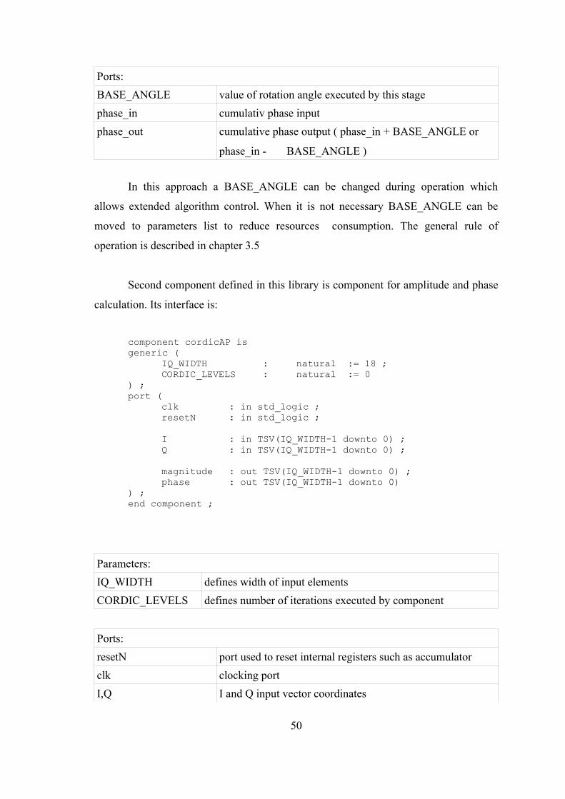
Ports:BASE_ANGLE value of rotation angle executed by this stagephase_in cumulativ phase inputphase_out cumulative phase output ( phase_in + BASE_ANGLE or
phase_in - BASE_ANGLE )
In this approach a BASE_ANGLE can be changed during operation which
allows extended algorithm control. When it is not necessary BASE_ANGLE can be
moved to parameters list to reduce resources consumption. The general rule of
operation is described in chapter 3.5
Second component defined in this library is component for amplitude and phase
calculation. Its interface is:
component cordicAP isgeneric (
IQ_WIDTH : natural := 18 ;CORDIC_LEVELS : natural := 0
) ;port (
clk : in std_logic ;resetN : in std_logic ;
I : in TSV(IQ_WIDTH-1 downto 0) ;Q : in TSV(IQ_WIDTH-1 downto 0) ;
magnitude : out TSV(IQ_WIDTH-1 downto 0) ;phase : out TSV(IQ_WIDTH-1 downto 0)
) ;end component ;
Parameters:IQ_WIDTH defines width of input elementsCORDIC_LEVELS defines number of iterations executed by component
Ports:resetN port used to reset internal registers such as accumulatorclk clocking portI,Q I and Q input vector coordinates
50

Ports:magnitude magnitude result of input vectorphase phase result for IQ vector
This component creates multiple instances of CORDIC stage entity to execute
several iterations of CORDIC algorithm. The description can be found in chapter 3.6
4.7 SRT
This library consists of the following components with the same interface, which
execute a single iteration of the SRT algorithm
First component executes single step of radix-2 srt algorithm:
component srt_stage2 isgeneric (
WORD_WIDTH : natural := 18) ;
port ( clk : in std_logic ;resetN : in std_logic ;
Pin : in TSV(WORD_WIDTH-1 downto 0) ;Pout : out TSV(WORD_WIDTH-1 downto 0) ;
D : in std_logic_vector(WORD_WIDTH-1 downto 0) ;Dout : out std_logic_vector(WORD_WIDTH-1 downto 0) ;
i_result : in TSV(WORD_WIDTH-1 downto 0) ;o_result : out TSV(WORD_WIDTH-1 downto 0));
end component;
The second one executes single step of radix-4 srt algorithm
component srt_stage4 isgeneric (
WORD_WIDTH : natural := 18) ;
51

port ( clk : in std_logic ;resetN : in std_logic ;
Pin : in TSV(WORD_WIDTH-1 downto 0) ;Pout : out TSV(WORD_WIDTH-1 downto 0) ;
D : in std_logic_vector(WORD_WIDTH-1 downto 0) ;Dout : out std_logic_vector(WORD_WIDTH-1 downto 0) ;
i_result : in TSV(WORD_WIDTH-1 downto 0) ;o_result : out TSV(WORD_WIDTH-1 downto 0));
end component;
Parameters:WORD_WIDTH defines width of input elements
Ports:resetN port used to reset internal registers such as accumulatorclk clocking portPin,Pout input partial remainder and output partial remainder after
iterationDin,Dout pipeline for divisori_result result calculated in previous iteration
o_result result updated in this iteration
The component is described in chapter 3.8. These components were used to
create a fixed point divisor which can execute a fixed point divison of numbers
normalized to the [0.5,1) range. Multiple instances of the SRT stage were used. Each
stage is capable of one ( SRT2 ) or 2 ( SRT4 ) digits of quotient calculation. It is defined
as follows:
component srt2/srt4 isgeneric (
WORD_WIDTH : natural := 18) ;
port ( clk : in std_logic ;resetN : in std_logic ;
52

D : in std_logic_vector(WORD_WIDTH-1 downto 0) ;C : in std_logic_vector(WORD_WIDTH-1 downto 0) ;
W : out std_logic_vector(WORD_WIDTH-1 downto 0) ;R : out TSV(WORD_WIDTH downto 0) );
end component;
Parameters:WORD_WIDTH defines width of input elements and number of iterations
needed to get full result
Ports:resetN port used to reset internal registersclk clocking portD divisor inputC dividend inputW result
R remainder
4.8 Floating point unit
The floating point unit consists of 3 components capable of arithmetic operations
on floating point numbers ( compatible with IEEE 784 standard ). The interface of the
components is shown below.
component mult[div/sum]_float isport (
clk : in std_logic ;resetN : in std_logic ;
S1 : in std_logic ;S2 : in std_logic ;
E1 : in std_logic_vector(7 downto 0) ;E2 : in std_logic_vector(7 downto 0) ;
M1 : in std_logic_vector(22 downto 0) ;M2 : in std_logic_vector(22 downto 0) ;
53

S3 : out std_logic ;E3 : out std_logic_vector( 7 downto 0) ;M3 : out std_logic_vector(22 downto 0)
);end component ;
Ports:resetN port used to reset internal registersclk clocking portS1,S2 signs of operandsS3 sign of the resultE1,E2 exponents of operands
E3 exponent of result
M1,M2 mantisas of operands
M3 mantisa of reult
The components are fully pipelined therefore processing of the operands can
start before the result of the previous ones is ready. The structure of the components is
shown on Figure 24 and Figure 25.
54
Figure 24: Floating point multiplication/division structure
M1 M2
x or /
normalization
E1 E2
+
exponent correction
rounding
S1 S2
XOR
M3 E3 S3

A functional description of the floating point arithmetic operations can be found
in chapter 3.10.
4.9 FIR filter
This FIR filter is a flexible, programmable filter. Modifications of filter
parameters and filter order do not require program recompilation. The following
declaration shows component's interface.
Type Tparray is array(31 downto 0) of natural ;
component filter is generic (
WORD_WIDTH : natural := 18 ;MAX_ORDER : natural := 32
) ; port(
clk :in std_logic ;int_clk :in std_logic ;resetN :in std_logic ;
order :in natural ;coefficients :in TParray
55
Figure 25: Floating point adder structure
M1 M2
+ or sub
normalization
E1 E2
exponent correction
rounding
M3 E3S3
exponent decision
exchange block
S1 S2

in_data : in std_logic_vector(WORD_WIDTH-1 downto 0) ;out_data : out std_logic_vector(WORD_WIDTH-1 downto 0)
);end component;
Parameters:WORD_WIDTH defines width of input elementsMAX_ORDER defines maximum order of the filter ( set at compialtion time)
Ports:resetN port used to reset internal registersclk clocking portint_clk clocking port used for internal calculations order Actual order of the filtercoefficients table of coeficients
data_in data input for the filter
data_out filtered data
The maximum value of 'order' port is MAX_ORDER. When it exceeds this
parameter it is treated as MAX_ORDER. CLK and INT_CLK can be connected to the
same clock if the sampling speed needs to be exactly the same as processing speed.
The structure of the implemented filter is shown on Figure 26.
56
Figure 26: Structure of a programmable filter
x x x x
coeficients
cascade of adders
...
coefficientsfilter input
resu
lt

4.10 OPB wrapper
This component is based on a OPB peripheral template provided by XILINX. It
provides the OPB interface for components defined in the mathematical library or for
any user component. Typical transactions on the OPB bus is shown on Figure 27.
Wrapper defines a set of registers which are mapped into embedded system's
address space. Register can be connected to any signal in the VHDL code. The
component is compatible with the Xilinx EDK IP core definition so it can be added
to embedded system using a graphical tool. Internal structure of this wrapper is shown
in Figure 27.
57
Figure 27: OPB wrapper structure connected to OPB logic
reg1_in reg1_out reg2_in reg2_out regN_in regN_out...
memory mapping OPB interfaceOPB
user logic
4.11 Summary
As the result of the implementation of the concept shown in chapter 3, a flexible
mathematical library was created. It fulfills all the requirements for the system
described in chapter 2. The functional blocks such as IQ demodulator or magnitude and
phase calculation provide scalable and simple means to implement input stages of many
algorithms. Blocks for matrix multiplication, division and sine calculation can be used
in many different places inside the algorithm implementation ( for example inside
detuning algorithm implementation or controller structures ). The rest of the basic
blocks such as math_basic_signed or math_matrix modules can be used when
functionality not inluded in this library is needed. They allow low level algorithm
implementation.
All blocks were optimized to provide a resonable choice between performance
and resource usage according to possibilities in the target accelerator environment. After
and during implementation all modules were completly tested. Descriptions and the
results of tests are shown in chapter 5.
58

5. Tests of designed system
All parts of presented system were tested during implementation using VHDL
simulation environment ( Aldec ActiveHDL ). The test procedure is shown using the
matrix_mult_base component as example. The first step was the implementation of
the module. The layout of ActiveHDL design environment is shown on Figure 28.
The compilation process was initiated and completed successfully. Then the
input vectors were defined amd simulation started. The results are shown below.
59
Figure 28: VHDL simulation environment

In this case the parameters INPUT_WIDTH and ITEM_COUNT were set to 5.
The analysis of the simulation results shows that the component is working as planned:
The input column element was set to 1 for the whole simulation. The row
element was changing during 5 clock cycles: 1,10,1,11,1. According to the chapter 3.3
the result on the output should be: 1*1+10*1+11*1+1*1+1*1 = 24. This result was
received after 7 clock cycles from the beginning of operation. Two additional delay
cycles are caused by internal pipelined structure of the component. In the next step of
verification each module was synthesized and the maximum working frequency was
measured.
Moreover most of described modules were used and tested during the
implementation process of the cavity detuning measurement algorithm. The final
product was connected to real accelerator signals and real-time measurements were
made.
60
Figure 29: Simulation results

This chapter presents a sample process of algorithm development and the results
of measurements. The board used was the SIMCON3.1 board presented in Chapter 1.
5.1 Cavity detuning measurment – algorithm and implementation
During accelerator operations the resonance frequency of superconducting
cavity changes. High energy field deforms the cavity's shape ( Lorentz force detuning )
and surrounding environment ( cooling system, ground motion, traffic ) causes
excitation of mechanical models ( microphonics ). Frequency shift leads to cavity field
errors and should be detected and compensated.
In the general transfer function for one electrical mode in superconducting cavity
can be modeled as high Q bandpass described using following equation [7]:
x2 1 2
x02 x=0 1
2
y
The signals x and y can be represented as
x= x0e j t y= y0 e jt
where x0 and y0 are changing slowly ( envelope ) and exp function is changing
fast. Therefore the first order envelope equation is:
x0 −1 2
−i x0 =y
2i0where =0 −1
2
The translation to the polar coordinates using:
x=r e j y=e j
gives following equations:
r −r=1 2sin − and r1
2r= 1
2cos−
The first equation can be used to determine the frequency change as:
=r − 1
2sin −
r
The final mathematical formula that was implemented is:
61

=−2
newdphase−2 1 2
∣calcomplex forward∣∣complex probe∣
sin angle calcomplex forward−anglecomplex probe
newdphase – deriviate of probe signal phase
calcomplexforward - complex ( IQ ) signal representing calibrated forward power
complexprobe - complex ( IQ ) signal representing probe power
The complexforward is the result of calibration between forward and reflected signals:
calcomplex forward=Acomplex forwardBcomplex reflected
The structure of implemented algorithm is shown on Figure 30.
62
Figure 30: Structure of cavity detuning measurment implementation
forward probereflected
IQ demodulator IQ demodulatorIQ demodulator
x x
+
Magnitude and phase
Magnitude and phase
processing block filter block
final detuning result
external calibration parameters
signals are represented as IQ

The first blocks in the algorithm are IQ demodulators taken from the library.
Then the signal is connected to calibration block. Two libraries can be use there:
math_basic_signed – 8 multiplications and 4 additions/subtractions must be made or
math_complex – 2 complex multiplications and 2 additions must be made.
Signals are conected to magnitude and phase calculation block based on
CORDIC algorithm. After calculations, the phase output of the probe signal is
connected to derivate filter and all the signals are connected to the processing block
showed on Figure 31.
63
Figure 31: Structure of the processing block
forward magnitude forward phaseprobe magnitude
division
probe phase
-
sin
x
- filter input
result
sin table

Magnitudes of the probe and the forward signals are divided by the fixed point
divison block base on SRT modules and sine for the difference of the phases is
calculated. In this case table for sine function was used – delay is time critical so
CORDIC can not be used. Next divisor output and calculated sine is multiplied and
result of probe phase filtering i subtracted.
The algorithm was used to evaluate the performance of the basic functional
blocks:
a) IQ demodulator
The probe signal from the accelerator was sampled and connected to the IQ
demodulator block. The results are shown in Figure 32
64
Figure 32: Probe signal with I and Q signals
Sample numbers = time [us]0 200 400 600 800 1000 1200 1400 1600 1800 2000
-3000
-2000
-1000
0
1000
2000
sample number
valu
e
probe samples
I
Q
Sample numbers = time [us]
value

The absolute error of calculations is shown on Figure 33. It is caused by fixed
point representation of data in the FPGA.
b) Magnitude and phase calculations
Calculated I and Q signal was connected to the input of Magnitude and phase
block. The results are shown on Figure 34 The absolute error of magnitude calculation
is shown on Figure 36. In this case it is sum of quantization error caused be fixed point
representation and CORDIC algorithm error.
65
Figure 33: Absolute error of calculations
0 200 400 600 800 1000 1200 1400 1600 1800 2000-60
-40
-20
0
20
40
60
sample number
erro
r in
qua
nts
Sample numbers = time [us]
erro
r

66
Figure 34: Magnitude result
0 500 1000 1500 2000 25000
1000
2000
3000
4000
5000
6000
sample number
valu
ecalculated magnitude
magnitude after CORDIC GAIN compensation
Figure 35: Absolute error of magnitude calculations
Sample numbers = time [us]
value
Sample numbers = time [us]
erro
r
0 500 1000 1500 2000 2500-3
-2
-1
0
1
2
3
4
5
6
7
sample number
erro
r
calculation error in quants
erro
r
Sample numbers = time [us]

The next figure shows phase output of CORDIC block. Y axis is scaled in
radians
The error of the phase calculations is shown on Figure 37 Again it is sum of
quantization error and CORDIC algorithm error.
67
Figure 36: Phase calculations
0 500 1000 1500 2000 2500-3
-2
-1
0
1
2
3
4
sample number
phas
e [
rad
]
calculated phase
Sample numbers = time [us]
phas
e [ra
d]

c) division block
Calculated magnitudes are delivered to the input of division block. It was
configured to deliver values with 4.14 representation ( 4 bits for integer part of a
number, 14 bits for fractional part ). Maximum value on division output is 7.9999.
Input magnitudes are shown on Figure 38. The result of the division is shown on Figure
39.
68
Figure 37: Absolute error of phase calculations
0 200 400 600 800 1000 1200 1400 1600 1800 2000
-6
-4
-2
0
2
4
x 10-3
sample number
erro
r [
rad
]
absolute error of phase calculation
Sample numbers = time [us]
erro
r [ra
d]

69
Figure 38: Inputs of the division block
0 500 1000 1500 2000 25000
500
1000
1500
2000
2500
3000
3500
4000
sample number
valu
e
forward magnitude
probe magnitude
Figure 39: Division result
0 200 400 600 800 1000 1200 1400 1600 1800 2000-10
-5
0
5
10
15
20
25
sample number
valu
e
response of division block
real divison result
Sample numbers = time [us]
value
Sample numbers = time [us]
value

The division block output differs from real division result untill sample 190. It is
caused by chosen representation. When the real result is lower than 8, the response of
the block is valid. Absolute error of calculation is shown on Figure 40. It is caused by
quantization.
SIMCON 3.1 board was configured and connected to Cavity 5 in ACC4 VUV-
FEL module. Real time detuning measurements were taken. Sample results are shown
of Figures 41 and 42.
70
Figure 40: Absolute error of division block
0 200 400 600 800 1000 1200 1400 1600 1800 2000
-20
-15
-10
-5
0
5
x 10-3
sample number
erro
r
absolute error
Sample numbers = time [us]
erro
r

71
Figure 41: Detuning signal taken during measurments in VUV-FEL
Figure 42: Detuning signal taken during measurments in VUV-FEL
time [us]
Det
uning
valu
e [V
]
time [us]
Det
uning
valu
e [V
]

5.2 Floating point unit tests
The OPB wrapper is used to connect floating point units to the embedded
PowerPC processor. A program for the performance evaluation was written. Inputs to
the operation blocks were mapped to the address space. PowerPC performed following
tasks:
1. 10000000 floating point add/subtracts were executed using software
emulation provided by Xilinx PPC library. Mean time of single operation
was measured.
2. The same task was performed but using hardware cores
3. The process was repeated for multiplication and division
The results from serial console on PPC are shown below:
Table 7 summarizes the results
72
MULTIPLICATION STATS
software emulationsingle operation: 2404.072998hardware supportsingle operation: 289.000000
ADD/SUB STATS
software emulationsingle operation: 2347.683838hardware supportsingle operation: 286.000000
DIV STATS
software emulationsingle operation: 4824.583496hardware supportsingle operation: 407.000000

sum/sub mult divsoftware 2347.683838 2404.072998 4824.583496
hardware 286.000000 289.000000 407.000000
acceleration 8.2 8.31 11.85
Table 7: Floating point core evaluation
The times are shown in processor clock cycles ( PPC frequency is 300MHz,
OPB bus frequency is 100MHz). Most of hardware latency is caused by input/output
operation delays in PPC system.
5.3 Matrix multiplication tests
To evaluate performance of matrix_mult_base module, the following structure
for 20x20 matrix multiplication was implemented. It allows to upload matrix data into 2
input memories using the comunnication interface ( in this case Internal Interface ).
Multiplication is executed and result matrix is stored in output memory.
73
Figure 43: Implemented matrix multiplication
matrix Arow
memory
matrix Bcolumnmemory
matrix_mult_base
resultmemory
A*B
communication interfce
clksynch

The CLK/SYNCH block provides the clocking signal for mutiplication unit and
memories. Moreover it controls adresses delivered to the memories to provide
synchronization between rows and columns. The configuration of the multiplication unit
is following:
INPUT_WIDTH = 18 INTERNAL_WIDTH = 24OUTPUT_WIDTH= 18 ITEM_COUNT = 20 BASE=0
Presented unit was implemented using Virtex 2 Pro XC2VP30 chip. Following
performance was achieved.
Speed grade LUTs FlipFlops 18x18 mult Block RAM Maximumfreq.
-5 128 57 1 3 90 MHz-6 128 57 1 3 100 MHz-7 128 57 1 3 115 MHz
Table 8: Performance and resource usage of matrix multiplication unit
Resource usage does not include resources used by comunication interface. The
calculation of one element takes 20 clock cycles. The whole result matrix with 400
element takes 8000 clock cycles. Additional 2 clock cycles are needed. The final result
is known after 8002 clock cycles. For -6 speed grade when the clock period is 10ns it
takes 80020 ns ( 80,02 us ). Table 9 shows multiplication time for a different number of
used hardware multipliers
Number of multipliers Operation time [us]1 802 404 208 10
Table 9: Matrix 20x20 multiplication time
74

6. Summary and conclusions
Presented library is now in testing stage. Initial tests and first algorithm
implementations showed that the base concept is correct and can be used in future
development. The following group of the system were implemented and tested – they
are accessible for end-user:
– input modules - ( they include IQ demodulator and Magnitude and phase
calculations ) which provide easy conversion of raw data into neccessary
representation. These modules execute input stages of many algorithms and provide
data for core modules which execute main calculations
– core modules – they execute specific functionality such as divison, sin/cos
calculation, data filtering. They can be conected to each other or to input modules to
create structure neccessary for specific algorithm implementation.
– embedded systems support – they provide interface to the embedded system, which
allows to connect and map any other module into embedded system's addres space
and floating point module to provide floating point arithmetical operations. Future
tests with embedded DOOCS servers that need fast floatng point operations may
show the real value of these modules
– low level modules ( they include libraries such as math_basic_signed,
math_complex, etc. ) which allow to implement any functionality which is not
included into other modules. They implement basic concepts of mathematical
library such as saturation arithmetic, complex numbers operation and so on. User
can easily implement his own modules without special considerations
All blocks were optimized to provide resonable choice between performance and
resource usage according to possibilities in target accelerator environment, but in future
versions of this library they can be further optimized to fit to the changing needs of the
75

system. Performance will change together with FPGA market changes and some
resource constraints may be dropped ( when the prices of FPGA chips decrease and
available resources increase ). Moreover the functional blocks written by the author or
end-users may be added to fit the needs of other groups and environments. The
proposed solution provides easy and fast way to implement algorithms, so it will easily
be integrated with existing systems. Architecture of the library is open so, in future,
components will be upgraded and new elements added.
76
References
[1] T. Czarski, K. Pozniak, R. Romaniuk S. Simrock: TESLA Cavity Modeling and
Digital Implementation with FPGA Technology Solution for Control System Purpose.
TESLA internal note 2003-28.
[2] W. Giergusiewicz,W. Koprek,W. Jalmuzna, K. T. Pozniak, R. S. Romaniuk FPGA
Based, DSP Integrated, 8-Channel SIMCON, ver. 3.0. Initial Results for 8-Channel
Algorithm. Tesla internal note 2005-14.
[3] T. Czarski, R. S. Romaniuk, K. T. Pozniak, S. Simrock: Cavity control system:
optimization methods for single cavity driving and envelope detection, Proceedings of
SPIE, Bellingham, WA, USA, Vol. 5484, 2004, pp. 99-110.
[4] Krzysztof T. Pozniak, Ryszard S. Romaniuk Modular and Reconfigurable Common
PCBPlatform of FPGA Based LLRF Control System for TESLA Test Facility, TESLA
Report 2005-04.
[5] W.M. Zabolotny, T. Czarski, T. Jezynski, K.T. Pozniak, P. Rutkowski, R.S.
Romaniuk,K. Bunkowski, FPGA Based Cavity Siumulator for TESLA Test Facility,
TESLA Report 2003-22.
[6] FPGA and Optical Network Based LLRF Distributed Control System for TESLA-
XFEL Linear Accelerator - Krzysztof T. Pozniak, Ryszard S. Romaniuk, Tomasz
Czarski, Wojciech Giergusiewicz, Wojciech Jalmuzna, Krzysztof Olowski, Karol
Perkuszewski, Jerzy Zielinski - Institute of Electronic Systems, Warsaw University of
Technology; Stefan Simrock – Tesla internal note 2004-09
[7] Thomas Schilcher ,Vector Sum Control of Pulsed Accelerating Fields in Lorentz
Force Detuned Superconducting Cavities
77

[8] Waldemar Koprek, Pawel Kaleta, Jaroslaw Szewinski, Krzysztof T.Pozniak,
Ryszard S. Romaniuk: Software Layer for SIMCON ver. 1.1., FPGA based TESLA
Cavity Control System; USER’S MANUAL. TESLA internal note 2005-05.
[9] 5.K. T. Pozniak, M. Bartoszek, M. Pietrusinski, Internal interface for RPC muon
trigger electronics at CMS experiment, Proceedings of SPIE, Bellingham, WA, USA,
Vol. 5484, 2004, pp. 269-282.
[10] Krzysztof Pozniak - INTERNAL INTERFACE, I/O Communication with FPGA
Circuits and Hardware Description Standard for Applications in HEP and FEL
Electronics ver. 1.0 - Tesla internal note 2005-22.
[11] Ray Andraka - A survey of CORDIC algorithms for FPGA based computers
[12] David L. Harris, Stuart F. Oberman, and Mark A. Horowitz- SRT Division
Architectures and Implementations
[13] J. Szabatin Podstawy teorii sygnałów, WKŁ 2003
[14] T. P. Zielińnski Od teorii do cyfrowego przetwarzania sygnałów,Wydawnictwo
AGH 2002.
[15] www.desy.de – DESY homepage.
[16] tesla.desy.de – TESLA homepage.
[17] www.xilinx.com – homepage of manufacturer of FPGA chips
[18] www.altera.com - homepage of manufacturer of FPGA chips
[19] www.opencores.org – FPGA resources webpage
[20] www.ieee.org – IEEE homepage
78

Acknowledgments
Author would like to thank everyone, who helped him during realisation of this
M.Sc.Thesis. Especially: Ph.D. Ryszard Romaniuk, Ph.D. Krzysztof Pozniak from
Warsaw University of Technology and Ph.D. Stefan Simrock and Alexander Brandt
from Deutches Electronen Synchrotron (Hamburg) for their supervision and opportunity
for projects to be started.
Author would like to thank ALDEC company for the opportunity to use their
ActiveHDL software for FPGA simulations.
Author would like to thank DESY Directorate, especially dr. Alexander Gamp,
for providing superb technical, financial and social conditions, for the TESLA LLRF
Group and the ELHEP Warsaw Group, to perform the work described in this paper.
79

7. Appendixes
80