Embed Size (px)
Citation preview
TPS61180/1/2
www.ti.com SLVS801E –DECEMBER 2007–REVISED APRIL 2013
WLED DRIVER FOR NOTEBOOK DISPLAYCheck for Samples: TPS61180/1/2
1FEATURES• 5 V to 24 V Input Voltage • Driver for Input/Output Isolation PFET• Integrated 1.5 A 40 V MOSFET • True Shutdown• 1.0 MHz/1.3 MHz Switching Frequency • Over Voltage Protection• Boost Output Auto-Adaptive to WLED Voltages • WLED Open/Short Protection• Small External Components • Built-in Soft Start• Integrated Loop Compensation • 16L 3 mm×3 mm QFN• Six Current Sink of 25 mA
APPLICATIONS• Up to 10 WLED in Series• Notebook LCD Display Backlight• Less Than 3% Current Matching and Accuracy• UMPC LCD Display Backlight• Up to 1000:1 PWM Brightness DImming Range• Backlight for Media Form Factor LCD display• Minimized Output Ripple Under PWM Dimming
DESCRIPTIONThe TPS61180/1/2 ICs provide highly integrated solutions for media size LCD backlight. These devices have abuilt-in high efficiency boost regulator with integrated 1.5A/40V power MOSFET. The six current sink regulatorsprovide high precision current regulation and matching. In total, the device can support up to 60 WLED. Inaddition, the boost output automatically adjusts its voltage to the WLED forward voltage to improve efficiency.
The devices support pulse width modulation (PWM) brightness dimming. During dimming, the WLED current isturned on/off at the duty cycle and frequency determined by the PWM signal input on the DCRTL pin. Onepotential issue of PWM dimming is audible noises from the output ceramic capacitors. The TPS61180/1/2 familyis designed to minimize this output AC ripple across a wide dimming duty cycle and frequency range; therefore,reducing the audible noise.
The TPS61180/1/2 ICs provide a driver output for an external PFET connected between the input and inductor.During short circuit or over-current conditions, the ICs turn off the external PFET and disconnect the battery fromthe WLEDs. The PFET is also turned off during IC shutdown (true shutdown) to prevent any leakage current ofthe battery. The device also integrates over-voltage protection, soft-start and thermal shutdown.
The TPS61180 IC requires external 3.3V IC supply, while TPS61181 and TPS61182 ICs have a built-in linearregulator for the IC supply. All the devices are in a 3×3 mm QFN package.
1
Please be aware that an important notice concerning availability, standard warranty, and use in critical applications ofTexas Instruments semiconductor products and disclaimers thereto appears at the end of this data sheet.
PRODUCTION DATA information is current as of publication date. Copyright © 2007–2013, Texas Instruments IncorporatedProducts conform to specifications per the terms of the TexasInstruments standard warranty. Production processing does notnecessarily include testing of all parameters.
L1
10 HmQ1
D2
D1 C24.7 Fm
IFB1
IFB2
IFB3
IFB4
IFB5
IFB6
VO
SWFault
VBAT
Cin
EN
DCTRL
ISET
PGND
GND
R162 kW
TPS61181/2
C4
0.1 Fm
Optional
5 V to 24 V
C14.7 Fm
10 WLED in series,120 mA total
EN
PWM Dimming
R2
51Ω
C3
1 Fm
R3
100 kW
TPS61180/1/2
SLVS801E –DECEMBER 2007–REVISED APRIL 2013 www.ti.com
This integrated circuit can be damaged by ESD. Texas Instruments recommends that all integrated circuits be handled withappropriate precautions. Failure to observe proper handling and installation procedures can cause damage.
ESD damage can range from subtle performance degradation to complete device failure. Precision integrated circuits may be moresusceptible to damage because very small parametric changes could cause the device not to meet its published specifications.
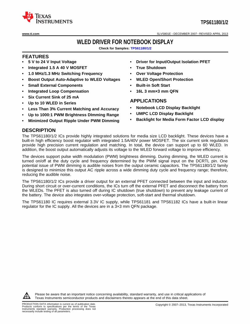
Figure 1. TPS61181/2 TYPICAL APPLICATION
ORDERING INFORMATION (1)
PACKAGE IC SUPPLY SWITCHING FREQUENCY PACKAGE MARKING(TYP)
TPS61180RTE External 3.3 V 1.0 MHz CCG
TPS61181RTE Built-in LDO 1.0 MHz CCH
TPS61182RTE Built-in LDO 1.3 MHz CCI
(1) For the most current package and ordering information, see the Package Option Addendum at the endof this document, or see the TI website at www.ti.com.
2 Submit Documentation Feedback Copyright © 2007–2013, Texas Instruments Incorporated
Product Folder Links: TPS61180/1/2
DCTRL
IFB
2
IFB
1
IFB3
Cin
SW
VO
5
EN
ISE
TF
ault
9
PGND
IFB
5
13
1
GND
IFB
6
IFB4
2
3
4
6 7 8
10
11
12
141516
QFN PACKAGE16 Pin 3x3
(TOP VIEW)
VBAT
TPS61180/1/2
www.ti.com SLVS801E –DECEMBER 2007–REVISED APRIL 2013
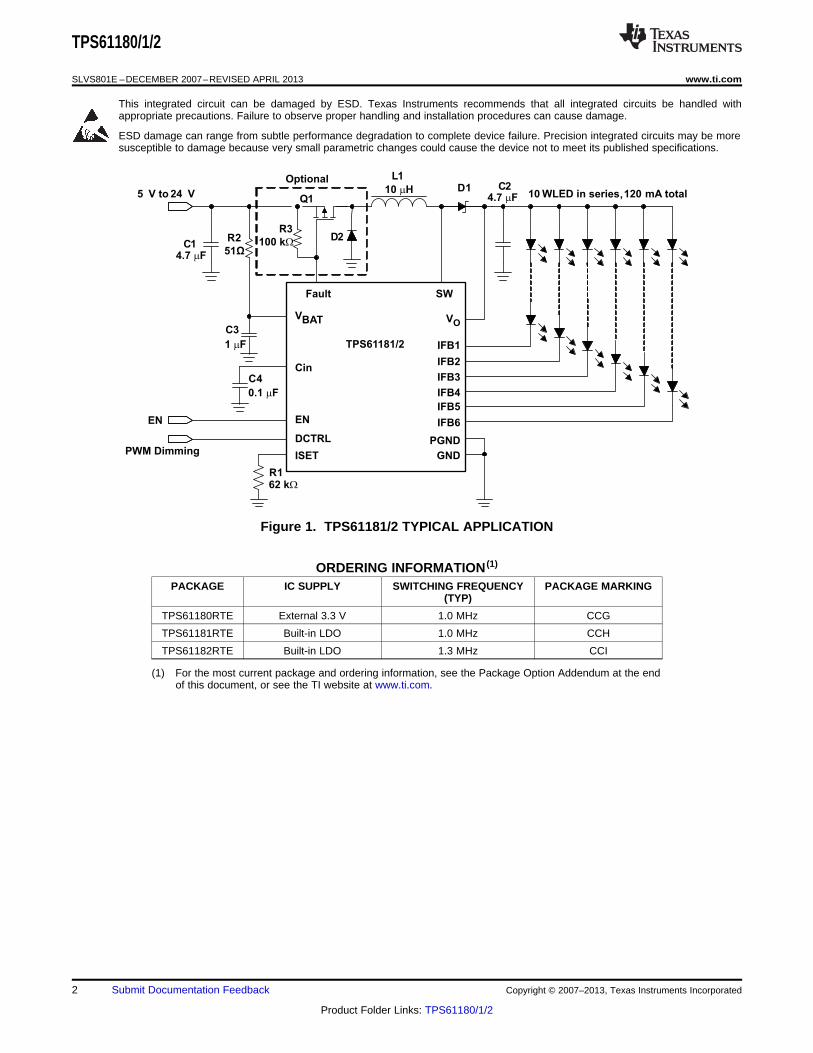
PINOUT
TERMINAL FUNCTIONSTERMINAL I/O DESCRIPTION
NO. NAME
1 PGND I Power ground of the IC. Internally, it connects to the source of the PWM switch.
2 SW I This pin connects to the drain of the internal PWM switch, external Schottky diode and inductor.
3 VBAT I This pin is connected to the battery supply. It provides the pull-up voltage for the Fault pin and batteryvoltage signal. For TPS61181/2, this is also the input to the internal LDO.
4 VO O This pin monitors the output of the boost regulator. Connect this pin to the anode of the WLED strings.
5 ISET I The resistor on this pin programs the WLED output current.
6 Cin I Supply voltage of the IC. For TPS61181/2, it is the output of the internal LDO. Connect 0.1 μF bypasscapacitor to this pin. For TPS61180, connect an external 3.3 V supply to power the IC.
7, 8, 9 IFB1-IFB3 I Current sink regulation inputs. They are connected to the cathode of WLEDs. The PWM loop regulates12, 13, 14 IFB4-IFB6 the lowest VIFB to 400 mV. Each channel is limited to 25 mA current.
10 GND I Signal ground of the IC.
11 DCTRL I Dimming control logic input. The dimming frequency range is 100 Hz to 1 kHz.
15 EN I The enable pin to the IC. For TPS61181/2, a logic high signal turns on the internal LDO and enables theIC. Therefore, do not connect the EN pin to the Cin pin.
16 Fault I Gate driver output for an external PFET used for fault protection. It can also be used as signal output forsystem fault report.
Copyright © 2007–2013, Texas Instruments Incorporated Submit Documentation Feedback 3
Product Folder Links: TPS61180/1/2
C24.7 Fm
IFB1
IFB2
IFB3
IFB4
IFB5IFB6
VOSW
PGND
GND
10 WLED in series,120 mA total
Current
Regulator
Dimming
Control
L1
10 HmQ1
D2
Cin
C4
0.1 Fm
Optional
Current Mode
PWM Control
IFB 1... IFB 6Fault
Protection
5 V to 24 V
C14.7 Fm
R3
51 W
C3
1 Fm
Internal Regulator
(TPS61181/2 only)
EN
PWM Dimming
Fault
ISET
VBAT
EN
DCTRL
D1
R1
R3
100 kW
TPS61180/1/2
SLVS801E –DECEMBER 2007–REVISED APRIL 2013 www.ti.com
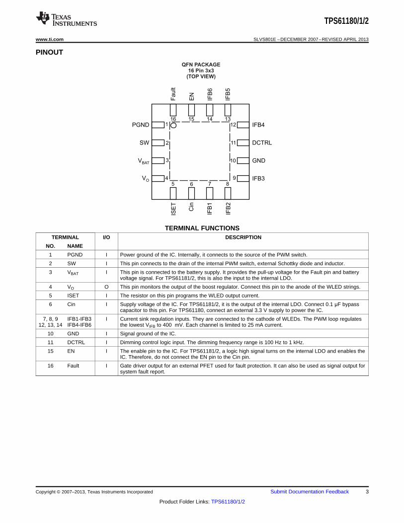
FUNCTIONAL BLOCK DIAGRAM
ABSOLUTE MAXIMUM RATINGSover operating free-air temperature range (unless otherwise noted) (1)
VALUE UNIT
Voltages on pin VBAT and Fault (2) –0.3 to 24 V
Voltage on pin Cin (2) –0.3 to 3.6 V
Voltage on pin SW and VO(2) –0.3 to 40 V
Voltage on pin IFB1 to IFB6 (2) –0.3 to 20 V
Voltage on all other pins (2) –0.3 to 7 V
Continuous power dissipation See Dissipation Rating Table
Operating junction temperature range –40 to 150 °C
Storage temperature range –65 to 150 °C
(1) Stresses beyond those listed under absolute maximum ratings may cause permanent damage to the device. These are stress ratingsonly, and functional operation of the device at these or any other conditions beyond those indicated under recommended operatingconditions is not implied. Exposure to absolute-maximum-rated conditions for extended periods may affect device reliability.
(2) All voltage values are with respect to network ground terminal.
DISSIPATION RATINGSPACKAGE RθJA TA ≤ 25°C TA = 70°C TA = 85°C
POWER RATING POWER RATING POWER RATING
TPS61180/1/2RTE (1) 270°C/W 370 mW 204 mW 148 mW
TPS61180/1/2RTE (2) 48.7°C/W 2.05 W 1.13 W 821 mW
(1) The JEDEC low-K (1s) board used to derive this data was a 3in×3in, two-layer board with 2-ounce copper traces on top of the board.(2) The JEDEC high-K (2s2p) board used to derive this data was a 3in×3in, multilayer board with 1-ounce internal power and ground.
4 Submit Documentation Feedback Copyright © 2007–2013, Texas Instruments Incorporated
Product Folder Links: TPS61180/1/2
TPS61180/1/2
www.ti.com SLVS801E –DECEMBER 2007–REVISED APRIL 2013
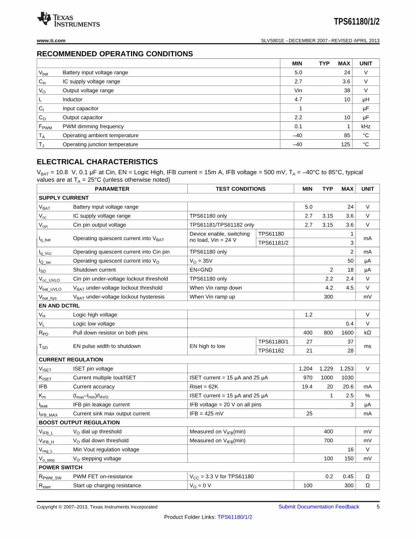
RECOMMENDED OPERATING CONDITIONSMIN TYP MAX UNIT
Vbat Battery input voltage range 5.0 24 V
Cin IC supply voltage range 2.7 3.6 V
VO Output voltage range Vin 38 V
L Inductor 4.7 10 μH
CI Input capacitor 1 μF
CO Output capacitor 2.2 10 μF
FPWM PWM dimming frequency 0.1 1 kHz
TA Operating ambient temperature –40 85 °C
TJ Operating junction temperature –40 125 °C
ELECTRICAL CHARACTERISTICSVBAT = 10.8 V, 0.1 μF at Cin, EN = Logic High, IFB current = 15m A, IFB voltage = 500 mV, TA = –40°C to 85°C, typicalvalues are at TA = 25°C (unless otherwise noted)
PARAMETER TEST CONDITIONS MIN TYP MAX UNIT
SUPPLY CURRENT
VBAT Battery input voltage range 5.0 24 V
Vcc IC supply voltage range TPS61180 only 2.7 3.15 3.6 V
Vcin Cin pin output voltage TPS61181/TPS61182 only 2.7 3.15 3.6 V
Device enable, switching TPS61180 1Iq_bat Operating quiescent current into VBAT mAno load, Vin = 24 V TPS61181/2 3
Iq_Vcc Operating quiescent current into Cin pin TPS61180 only 2 mA
IQ_sw Operating quiescent current into VO VO = 35V 50 μA
ISD Shutdown current EN=GND 2 18 μA
Vcc_UVLO Cin pin under-voltage lockout threshold TPS61180 only 2.2 2.4 V
Vbat_UVLO VBAT under-voltage lockout threshold When Vin ramp down 4.2 4.5 V
Vbat_hys VBAT under-voltage lockout hysteresis When Vin ramp up 300 mV
EN AND DCTRL
VH Logic high voltage 1.2 V
VL Logic low voltage 0.4 V
RPD Pull down resistor on both pins 400 800 1600 kΩTPS61180/1 27 37
TSD EN pulse width to shutdown EN high to low msTPS61182 21 28
CURRENT REGULATION
VISET ISET pin voltage 1.204 1.229 1.253 V
KISET Current multiple Iout/ISET ISET current = 15 μA and 25 μA 970 1000 1030
IFB Current accuracy Riset = 62K 19.4 20 20.6 mA
Km (Imax–Imin)/IAVG ISET current = 15 μA and 25 μA 1 2.5 %
Ileak IFB pin leakage current IFB voltage = 20 V on all pins 3 μA
IIFB_MAX Current sink max output current IFB = 425 mV 25 mA
BOOST OUTPUT REGULATION
VIFB_L VO dial up threshold Measured on VIFB(min) 400 mV
VIFB_H VO dial down threshold Measured on VIFB(min) 700 mV
Vreg_L Min Vout regulation voltage 16 V
Vo_step VO stepping voltage 100 150 mV
POWER SWITCH
RPWM_SW PWM FET on-resistance VCC = 3.3 V for TPS61180 0.2 0.45 ΩRstart Start up charging resistance VO = 0 V 100 300 Ω
Copyright © 2007–2013, Texas Instruments Incorporated Submit Documentation Feedback 5
Product Folder Links: TPS61180/1/2
TPS61180/1/2
SLVS801E –DECEMBER 2007–REVISED APRIL 2013 www.ti.com
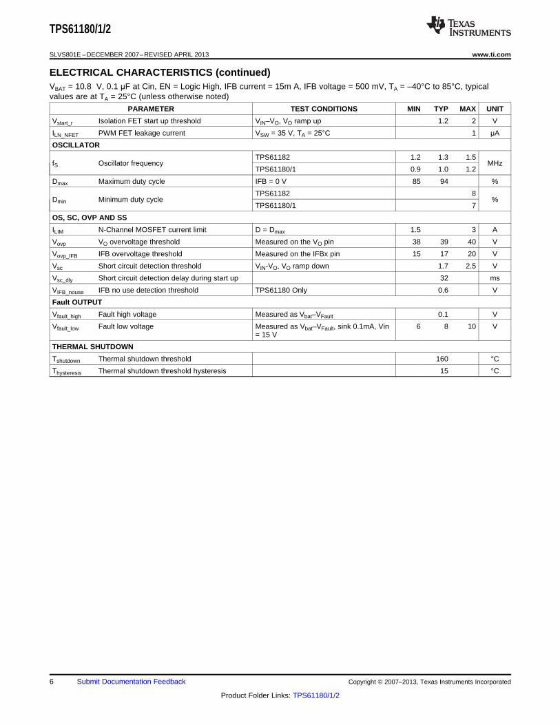
ELECTRICAL CHARACTERISTICS (continued)VBAT = 10.8 V, 0.1 μF at Cin, EN = Logic High, IFB current = 15m A, IFB voltage = 500 mV, TA = –40°C to 85°C, typicalvalues are at TA = 25°C (unless otherwise noted)
PARAMETER TEST CONDITIONS MIN TYP MAX UNIT
Vstart_r Isolation FET start up threshold VIN–VO, VO ramp up 1.2 2 V
ILN_NFET PWM FET leakage current VSW = 35 V, TA = 25°C 1 μA
OSCILLATOR
TPS61182 1.2 1.3 1.5fS Oscillator frequency MHz
TPS61180/1 0.9 1.0 1.2
Dmax Maximum duty cycle IFB = 0 V 85 94 %
TPS61182 8Dmin Minimum duty cycle %
TPS61180/1 7
OS, SC, OVP AND SS
ILIM N-Channel MOSFET current limit D = Dmax 1.5 3 A
Vovp VO overvoltage threshold Measured on the VO pin 38 39 40 V
Vovp_IFB IFB overvoltage threshold Measured on the IFBx pin 15 17 20 V
Vsc Short circuit detection threshold VIN-VO, VO ramp down 1.7 2.5 V
Vsc_dly Short circuit detection delay during start up 32 ms
VIFB_nouse IFB no use detection threshold TPS61180 Only 0.6 V
Fault OUTPUT
Vfault_high Fault high voltage Measured as Vbat–VFault 0.1 V
Vfault_low Fault low voltage Measured as Vbat–VFault, sink 0.1mA, Vin 6 8 10 V= 15 V
THERMAL SHUTDOWN
Tshutdown Thermal shutdown threshold 160 °C
Thysteresis Thermal shutdown threshold hysteresis 15 °C
6 Submit Documentation Feedback Copyright © 2007–2013, Texas Instruments Incorporated
Product Folder Links: TPS61180/1/2
80
82
84
86
88
90
92
94
96
98
100
0 25 50 75 100 125 150
I - Output Current - mAO
Eff
icie
ncy -
%
V = 11 Vbat
V = 28.8 VO
V = 17.6 VO
V = 23.2 VO
80
82
84
86
88
90
92
94
96
98
100E
ffic
ien
cy -
%
0 25 50 75 100 125 150
I - Output Current - mAO
V = 11 Vbat
V = 31.6 VO
V = 36.2 VO
TPS61180/1/2
www.ti.com SLVS801E –DECEMBER 2007–REVISED APRIL 2013
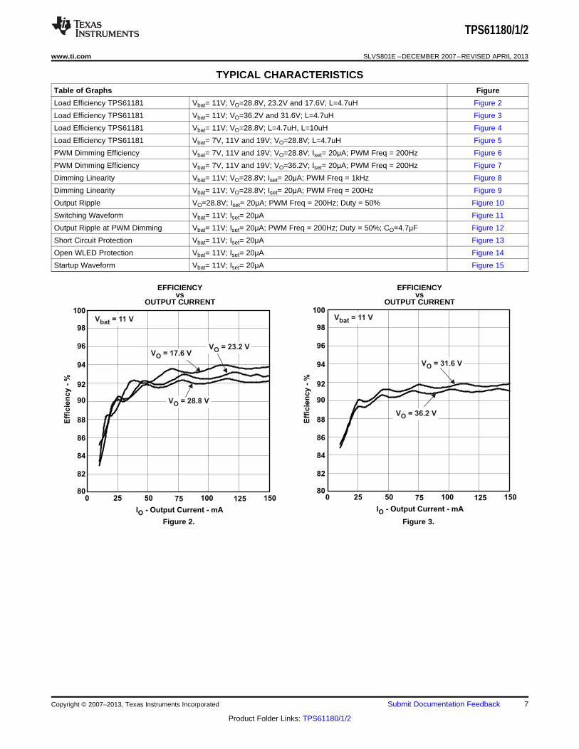
TYPICAL CHARACTERISTICSTable of Graphs Figure
Load Efficiency TPS61181 Vbat= 11V; VO=28.8V, 23.2V and 17.6V; L=4.7uH Figure 2
Load Efficiency TPS61181 Vbat= 11V; VO=36.2V and 31.6V; L=4.7uH Figure 3
Load Efficiency TPS61181 Vbat= 11V; VO=28.8V; L=4.7uH, L=10uH Figure 4
Load Efficiency TPS61181 Vbat= 7V, 11V and 19V; VO=28.8V; L=4.7uH Figure 5
PWM Dimming Efficiency Vbat= 7V, 11V and 19V; VO=28.8V; Iset= 20μA; PWM Freq = 200Hz Figure 6
PWM Dimming Efficiency Vbat= 7V, 11V and 19V; VO=36.2V; Iset= 20μA; PWM Freq = 200Hz Figure 7
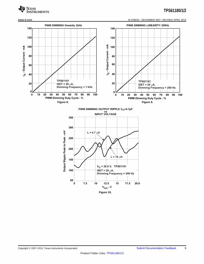
Dimming Linearity Vbat= 11V; VO=28.8V; Iset= 20μA; PWM Freq = 1kHz Figure 8
Dimming Linearity Vbat= 11V; VO=28.8V; Iset= 20μA; PWM Freq = 200Hz Figure 9
Output Ripple VO=28.8V; Iset= 20μA; PWM Freq = 200Hz; Duty = 50% Figure 10
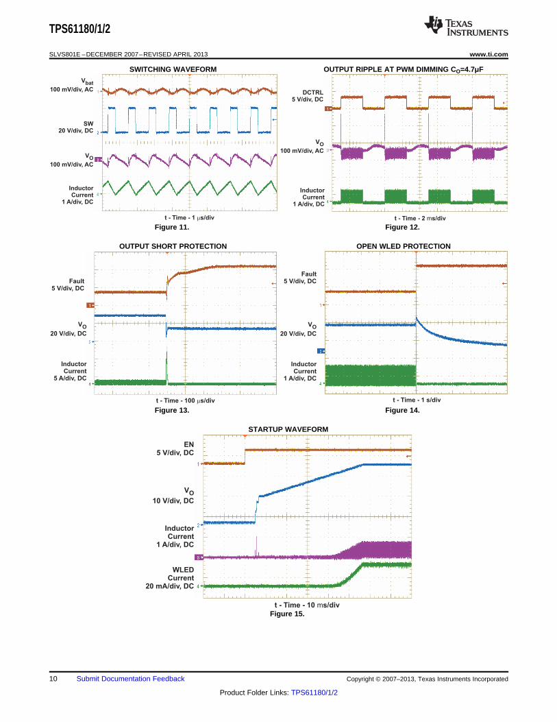
Switching Waveform Vbat= 11V; Iset= 20μA Figure 11
Output Ripple at PWM Dimming Vbat= 11V; Iset= 20μA; PWM Freq = 200Hz; Duty = 50%; CO=4.7μF Figure 12
Short Circuit Protection Vbat= 11V; Iset= 20μA Figure 13
Open WLED Protection Vbat= 11V; Iset= 20μA Figure 14
Startup Waveform Vbat= 11V; Iset= 20μA Figure 15
EFFICIENCY EFFICIENCYvs vs
OUTPUT CURRENT OUTPUT CURRENT
Figure 2. Figure 3.
Copyright © 2007–2013, Texas Instruments Incorporated Submit Documentation Feedback 7
Product Folder Links: TPS61180/1/2
50
60
70
80
90
100
0 10 20 30 40 50 60 70 80 90 100
PWM Dimming Duty Cycle - %
V = 11 Vbat
Eff
icie
ncy -
%
V = 19 Vbat
V = 7 Vbat
V = 28.8 V, TPS61181
ISET = 20 A,Dimming Frequency = 200 Hz
O
m
50
60
70
80
90
100
0 10 20 30 40 50 60 70 80 90 100
PWM Dimming Duty Cycle - %
Eff
icie
ncy -
%
V = 36.2 V - TPS61181
ISET = 20 ADimming Frequency = 200 Hz
O
m
V = 19 Vbat
V = 11 Vbat
V = 7 Vbat
80
82
84
86
88
90
92
94
96
98
100
Eff
icie
ncy -
%
0 25 50 75 100 125 150
I - Output Current - mAO
V = 11 Vbat
10 Hm
4.7 Hm
V = 28.8 V,
TPS61181O
80
82
84
86
88
90
92
94
96
98
100
Eff
icie
ncy -
%
0 25 50 75 100 125 150
I - Output Current - mAO
V = 7 Vbat
V = 19 VbatV = 11 Vbat
V = 28.8 V,
TPS61181O
TPS61180/1/2
SLVS801E –DECEMBER 2007–REVISED APRIL 2013 www.ti.com
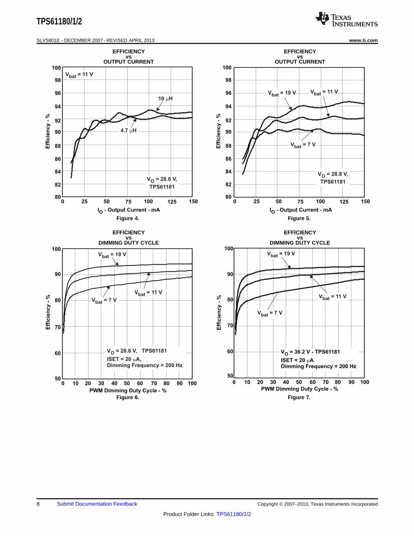
EFFICIENCY EFFICIENCYvs vs
OUTPUT CURRENT OUTPUT CURRENT
Figure 4. Figure 5.
EFFICIENCY EFFICIENCYvs vs
DIMMING DUTY CYCLE DIMMING DUTY CYCLE
Figure 6. Figure 7.
8 Submit Documentation Feedback Copyright © 2007–2013, Texas Instruments Incorporated
Product Folder Links: TPS61180/1/2
50
100
150
200
250
300
350
5 7.5 12.5 15 17.5 20.0
Ou
tpu
t R
ipp
le P
eak t
o P
eak -
mV
10
V - Vbat
V = 28.8 V, TPS61181
ISET = 20 A,Dimming Frequency = 200 Hz
O
m
L = 4.7 Hm
L = 10 Hm
0
20
40
60
80
100
120
140
0 10 20 30 40 50 60 70 80 90 100
PWM Dimming Duty Cycle - %
I-
Ou
tpu
t C
urr
en
t -
mA
O
TPS61181
ISET = 20 A,Dimming Frequency = 200 Hz
m
0
20
40
60
80
100
120
140
0 10 20 30 40 50 60 70 80 90 100
PWM Dimming Duty Cycle - %
I-
Ou
tpu
t C
urr
en
t -
mA
O
TPS61181
ISET = 20 A,Dimming Frequency = 1 kHz
m
TPS61180/1/2
www.ti.com SLVS801E –DECEMBER 2007–REVISED APRIL 2013
PWM DIMMING linearity 1kHz PWM DIMMING LINEARITY 200Hz
Figure 8. Figure 9.
PWM DIMMING OUTPUT RIPPLE CO=4.7μFvs
INPUT VOLTAGE
Figure 10.
Copyright © 2007–2013, Texas Instruments Incorporated Submit Documentation Feedback 9
Product Folder Links: TPS61180/1/2
V
10 V/div, DCO
Inductor
Current
1 A/div, DC
t - Time - 10 s/divm
EN
5 V/div, DC
WLED
Current
20 mA/div, DC
V
20 V/div, DCO
Inductor
Current
5 A/div, DC
Fault
5 V/div, DC
t - Time - 100 s/divm
Fault
5 V/div, DC
V
20 V/div, DCO
Inductor
Current
1 A/div, DC
t - Time - 1 s/div
V
100 mV/div, ACbat
SW
20 V/div, DC
V
100 mV/div, ACO
Inductor
Current
1 A/div, DC
t - Time - 1 s/divm
V
100 mV/div, ACO
Inductor
Current
1 A/div, DC
t - Time - 2 s/divm
DCTRL
5 V/div, DC
TPS61180/1/2
SLVS801E –DECEMBER 2007–REVISED APRIL 2013 www.ti.com
SWITCHING WAVEFORM OUTPUT RIPPLE AT PWM DIMMING CO=4.7μF
Figure 11. Figure 12.
OUTPUT SHORT PROTECTION OPEN WLED PROTECTION
Figure 13. Figure 14.
STARTUP WAVEFORM
Figure 15.
10 Submit Documentation Feedback Copyright © 2007–2013, Texas Instruments Incorporated
Product Folder Links: TPS61180/1/2
TPS61180/1/2
www.ti.com SLVS801E –DECEMBER 2007–REVISED APRIL 2013
DETAILED DESCRIPTION
Recently, WLEDs have gained popularity as an alternative to CCFL for backlighting media size LCD displays.The advantages of WLEDs are power efficiency and low profile design. Due to the large number of WLEDs, theyare often arranged in series and parallel, and powered by a boost regulator with multiple current sink regulators.Having more WLEDs in series reduces the number of parallel strings and therefore improves overall currentmatching. However, the efficiency of the boost regulator declines due to the need for high output voltage. Also,there have to be enough WLEDs in series to ensure the output voltage stays above the input voltage range.Otherwise, a buck-boost (for example, SEPIC) power converter has to be adopted which could be moreexpensive and complicated.
The TPS61180/1/2 family of ICs have integrated all the key function blocks to power and control up to 60WLEDs. The devices include a 40V/1.5A boost regulator, six 25mA current sink regulators and protection circuitfor over-current, over-voltage and short circuit failures. The key advantages of the devices are small solutionsize, low output AC ripple during PWM dimming control, and the capability to isolate the input and output duringfault conditions.
SUPPLY VOLTAGE
The TPS61181/2 ICs have built-in LDO linear regulator to supply the IC analog and logic circuit. The LDO ispowered up when the EN pin is high. The output of the LDO is connected to the Cin pin. A 0.1μF bypasscapacitor is required for LDO’s stable operation. Do not connect the Cin pin to the EN pin because this preventsthe IC from starting up. In addition, avoid connecting the Cin pin to any other circuit as this could introduce noiseinto the IC supply voltage.
The TPS61180 has no built-in LDO linear regulator, and therefore requires an external supply voltage in therange of 2.7V to 3.6V connected to the Cin pin. The benefit of using external supply is to reduce the powerlosses incurred by the LDO as it provides the IC supply current. This loss could become a significant percentageof total output power under light load condition. The Cin pin has 2.2V (typical) under-voltage lock out which turnsoff the IC when the Cin pin voltage is below this threshold.
The voltage on the VBAT pin is the reference for the pull-up circuit of the Fault pin. In addition, it also serves asthe input signal to the short circuit protection. For TPS61181/2 ICs, the VBAT connects to the input of the internalLDO, and powers the IC. There is an under-voltage lockout on the VBAT pin which disables the IC when itsvoltage reduces to 4.2V (Typical). The IC restarts when the VBAT pin voltage recovers by 300mV.
BOOST REGULATOR
The boost regulator is controlled by current mode PWM, and loop compensation is integrated inside the IC. Theinternal compensation ensures stable output over the full input and output voltage range. The TPS61180/1switches at 1.0MHz, and the TPS61182 switches at 1.3MHz. The switching frequencies of the two devices,including their tolerance, due not over-lap. Therefore, in the unlikely event that one device createselectromagnetic inference to the system; the other device, switching at a different frequency, can provide analternative solution.
The output voltage of the boost regulator is automatically set by the IC to minimize the voltage drop across theIFB pins. The IC automatically regulates the lowest IFB pin to 400mV, and consistently adjusts the boost outputvoltage to account for any changes of the LED forward voltages.
When the output voltage is too close to the input, the boost regulator may not be able to regulate the output dueto the limitation of minimum duty cycle. In this case, increase the number of WLED in series or include seriesballast resistors in order to provide enough headroom for the boost operation.
The TPS61180/1/2 boost regulators cannot regulate their outputs to voltages below 15V.
Copyright © 2007–2013, Texas Instruments Incorporated Submit Documentation Feedback 11
Product Folder Links: TPS61180/1/2
IFB KISET
VISETRISET
TPS61180/1/2
SLVS801E –DECEMBER 2007–REVISED APRIL 2013 www.ti.com
CURRENT PROGRAM AND PWM DIMMING
The six current sink regulators can each provide maximum 25mA. The IFB current must be programmed tohighest WLED current expected using the ISET pin resistor and the following Equation 1.
(1)
WhereKISET = Current multiple (1000 typical)VISET = ISET pin voltage (1.229 V typical)RISET = ISET pin resistor
The TPS61180/1/2 ICs have built-in precise current sink regulator. The current matching among 6 current sinksis below 2.5%. This means the differential value between the maximum and minimum current of the six currentsinks divided by the average current of the six is less than 2.5%.
The WLED brightness is controlled by the PWM signal on the DCTRL pin. The frequency and duty cycle of theDCTRL signal is replicated on the IFB pin current. Keep the dimming frequency in the range of 100Hz to 1kHz toavoid screen flickering and maintain dimming linearity. Screen flickering may occur if the dimming frequency isbelow the range. The minimum achievable duty cycle increases with the dimming frequency. For example, whilea 0.1% dimming duty cycle, giving a 1000:1 dimming range, is achievable at 100 Hz dimming frequency, only 1%duty cycle, giving a 100:1 dimming range, is achievable with a 1 KHz dimming frequency, and 5% dimming dutycycle is achievable with 5KHz dimming frequency. The device could work at high dimming frequency like 20 KHz,but only 15% duty cycle could be achievable. The TPS61180/1/2 ICs are designed to minimize the AC ripple onthe output capacitor during PWM dimming. Careful passive component selection is also critical to minimize ACripple on the output capacitor. See APPLICATION INFORMATION for more information.
ENABLE AND START UP
A logic high signal on the EN pin turns on the IC. For the TPS61181/2 ICs, taking EN high turns on the internalLDO linear regulator which provides supply IC current. For all devices, an internal resistor Rstart (start up chargingresistor) is connected between the VBAT pin and VO pin to charge the output capacitor toward Vin. The Fault pinoutputs high during this time, and thus the external isolation PFET is turned off. Once the VO pin voltage is within2 V (isolation FET start up threshold) of the VBAT pin voltage, Rstart is open, and the Fault pin pulls down the gateof the PFET and connects the VBAT voltage to the boost regulator. This operation is to prevent the in-rush currentdue to charging the output capacitor.
Once the isolation FET is turned on, the IC starts the PWM switching to raise the output voltage above VBAT.Soft-start is implemented by gradually ramping up the reference voltage of the error amplifier to prevent voltageover-shoot and in-rush current. See the start-up waveform of a typical example, Figure 15.
Pulling the EN pin low for 32ms (typical) shuts down the IC, resulting in the IC consuming less than 50μA in theshutdown mode.
OVER-CURRENT, OVER-VOLTAGE AND SHORT-CIRCUIT PROTECTION
The TPS61180/1/2 family has pulse by pulse over-current limit of 1.5A (min). The PWM switch turns off when theinductor current reaches this current threshold. The PWM switch remains off until the beginning of the nextswitching cycle. This protects the IC and external component under over-load conditions. When there issustained over-current condition for more than 16ms ( under 100% dimming duty cycle), the IC turns off andrequires PER or the EN pin toggling to restart.
Under severe over-load and/or short circuit conditions, the VO pin can be pulled below the input (VBAT pin). Underthis condition, the current can follow directly from input to output through the inductor and Schottky diode.Turning off the PWM switch alone does not limit current anymore. In this case, the TPS61180/1/2 ICs detect theoutput voltage is 1V (short circuit detection threshold) below the input voltage, turns off the isolation FET, andshuts down the IC. The IC restarts after input power-on reset (VBAT POR) or EN pin logic toggling.
During the IC start up, if there is short circuit condition on the boost converter output, the output capacitor will notbe charged to within 2V of VBAT through Rstart. After 32ms (short circuit detection delay during start up), the ICshuts down and does not restart until there is VBAT POR or EN pin toggling. The isolation FET is never turned onunder the condition.
12 Submit Documentation Feedback Copyright © 2007–2013, Texas Instruments Incorporated
Product Folder Links: TPS61180/1/2
TPS61180/1/2
www.ti.com SLVS801E –DECEMBER 2007–REVISED APRIL 2013
For the TPS61181/2 ICs, if one of the WLED strings is open, the boost output rises to over-voltage threshold(39V typical). The IC detects the open WLED string by sensing no current in the corresponding IFB pin. As aresult, the IC removes the open IFB pin from the voltage feedback loop. Subsequently, the output voltage dropsdown and is regulated to a voltage for the connected WLED strings. The IFB current of the connected WLEDstring keeps in regulation during the whole transition. The IC only shuts down if it detects that all of the WLEDstrings are open.
For the TPS61180, if the IC detects any open WLED string, the IC shuts down and remains off until there is VBATPOR or EN pin toggling.
For all the devices, if the over-voltage threshold is reached, but the current sensed on the IFB pin is below theregulation target, the IC regulates the boost output at the over-voltage threshold. This operation could occurwhen the WLED is turned on under cold temperature, and the forward voltages of the WLEDs exceed the over-voltage threshold. Maintaining the WLED current allows the WLED to warm up and their forward voltages to dropbelow the over-voltage threshold.
For the TPS61181/2 ICs, if any IFB pin voltage exceeds IFB over-voltage threshold (17V typical), the IC turns offthe corresponding current sink and removes this IFB pin from VO regulation loop. The remaining IFB pins’ currentregulation is not affected. This condition often occurs when there are several shorted WLEDs in one string.WLED mismatch typically does not create such large voltage difference among WLED strings.
For the TPS61180 IC, if any IFB pin voltage exceeds IFB over-voltage threshold, the IC shuts down and remainsoff until there is VBAT POR or EN pin toggling.
IFB PIN UNUSED
If the application requires less than 6 WLED strings, one can easily disable unused IFB pins. The TPS61181/2ICs simply require leaving the unused IFB pin open or shorting it to ground. If the IFB pin is open, the boostoutput voltage ramps up to VO over-voltage threshold during start up. The IC then detects the zero current string,and removes it from the feedback loop. If the IFB pin is shorted to ground, the IC detects the short immediatelyafter IC enable, and the boost output voltage does not go up to VO over-voltage threshold. Instead, it ramps tothe regulation voltage after soft start.
For the TPS61180, connect a 10 kΩ resistor from the unused IFB pin to ground. After the device is enabled, theIC detects the resistor and disables the IFB pin from the feedback loop.
Copyright © 2007–2013, Texas Instruments Incorporated Submit Documentation Feedback 13
Product Folder Links: TPS61180/1/2
Ip IdcIpp2
Ipp 1
L 1VOVbat
1Vbat FS
IdcVO IOVin
TPS61180/1/2
SLVS801E –DECEMBER 2007–REVISED APRIL 2013 www.ti.com
APPLICATION INFORMATION
INDUCTOR SELECTION
Because the selection of the inductor affects power supply’s steady state operation, transient behavior and loopstability, the inductor is the most important component in switching power regulator design. There are threespecifications most important to the performance of the inductor, inductor value, DC resistance and saturationcurrent. The TPS61180/1/2 ICs are designed to work with inductor values between 4.7μH and 10μH. A 4.7μHinductor could be available in a smaller or lower profile package, while 10μH may produce higher efficiency dueto lower inductor ripple. If the boost output current is limited by the over-current protection of the IC, using a10μH inductor can offer higher output current.
The internal loop compensation for the PWM control is optimized for the recommended component values,including typical tolerances. Inductor values can have ±20% tolerance with no current bias. When the inductorcurrent approaches saturation level, its inductance can decrease 20 to 35% from the 0A value depending on howthe inductor vendor defines saturation
In a boost regulator, the inductor DC current can be calculated as
(2)
WhereVO = boost output voltageIo = boost output currentVin = boost input voltageη = power conversion efficiency, use 90% for TPS61180/1/2 applications
The inductor current peak to peak ripple can be calculated as
(3)
WhereIpp = inductor peak to peak rippleL = inductor valueFs= Switching frequencyVbat= boost input voltage
Therefore, the peak current seen by the inductor is
(4)
Select the inductor with saturation current over the calculated peak current. To calculate the worse case inductorpeak current, use minimum input voltage, maximum output voltage and maximum load current.
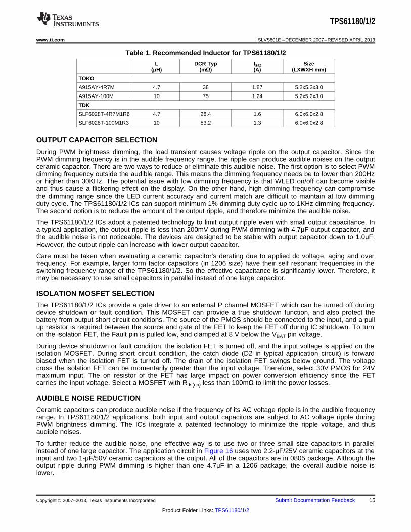
Regulator efficiency is dependent on the resistance of its high current path, switching losses associated with thePWM switch and power diode. Although the TPS61180/1/2 ICs have optimized the internal switch resistance, theoverall efficiency still relies on the DC resistance (DCR) of the inductor; lower DCR improves efficiency.However, there is a trade off between DCR and inductor footprint. Furthermore, shielded inductors typically havea higher DCR than unshielded ones. Table 1 lists recommended inductor models.
14 Submit Documentation Feedback Copyright © 2007–2013, Texas Instruments Incorporated
Product Folder Links: TPS61180/1/2
TPS61180/1/2
www.ti.com SLVS801E –DECEMBER 2007–REVISED APRIL 2013
Table 1. Recommended Inductor for TPS61180/1/2
L DCR Typ Isat Size(μH) (mΩ) (A) (LXWXH mm)
TOKO
A915AY-4R7M 4.7 38 1.87 5.2x5.2x3.0
A915AY-100M 10 75 1.24 5.2x5.2x3.0
TDK
SLF6028T-4R7M1R6 4.7 28.4 1.6 6.0x6.0x2.8
SLF6028T-100M1R3 10 53.2 1.3 6.0x6.0x2.8
OUTPUT CAPACITOR SELECTION
During PWM brightness dimming, the load transient causes voltage ripple on the output capacitor. Since thePWM dimming frequency is in the audible frequency range, the ripple can produce audible noises on the outputceramic capacitor. There are two ways to reduce or eliminate this audible noise. The first option is to select PWMdimming frequency outside the audible range. This means the dimming frequency needs be to lower than 200Hzor higher than 30KHz. The potential issue with low dimming frequency is that WLED on/off can become visibleand thus cause a flickering effect on the display. On the other hand, high dimming frequency can compromisethe dimming range since the LED current accuracy and current match are difficult to maintain at low dimmingduty cycle. The TPS61180/1/2 ICs can support minimum 1% dimming duty cycle up to 1KHz dimming frequency.The second option is to reduce the amount of the output ripple, and therefore minimize the audible noise.
The TPS61180/1/2 ICs adopt a patented technology to limit output ripple even with small output capacitance. Ina typical application, the output ripple is less than 200mV during PWM dimming with 4.7μF output capacitor, andthe audible noise is not noticeable. The devices are designed to be stable with output capacitor down to 1.0μF.However, the output ripple can increase with lower output capacitor.
Care must be taken when evaluating a ceramic capacitor’s derating due to applied dc voltage, aging and overfrequency. For example, larger form factor capacitors (in 1206 size) have their self resonant frequencies in theswitching frequency range of the TPS61180/1/2. So the effective capacitance is significantly lower. Therefore, itmay be necessary to use small capacitors in parallel instead of one large capacitor.
ISOLATION MOSFET SELECTION
The TPS61180/1/2 ICs provide a gate driver to an external P channel MOSFET which can be turned off duringdevice shutdown or fault condition. This MOSFET can provide a true shutdown function, and also protect thebattery from output short circuit conditions. The source of the PMOS should be connected to the input, and a pullup resistor is required between the source and gate of the FET to keep the FET off during IC shutdown. To turnon the isolation FET, the Fault pin is pulled low, and clamped at 8 V below the VBAT pin voltage.
During device shutdown or fault condition, the isolation FET is turned off, and the input voltage is applied on theisolation MOSFET. During short circuit condition, the catch diode (D2 in typical application circuit) is forwardbiased when the isolation FET is turned off. The drain of the isolation FET swings below ground. The voltagecross the isolation FET can be momentarily greater than the input voltage. Therefore, select 30V PMOS for 24Vmaximum input. The on resistor of the FET has large impact on power conversion efficiency since the FETcarries the input voltage. Select a MOSFET with Rds(on) less than 100mΩ to limit the power losses.
AUDIBLE NOISE REDUCTION
Ceramic capacitors can produce audible noise if the frequency of its AC voltage ripple is in the audible frequencyrange. In TPS61180/1/2 applications, both input and output capacitors are subject to AC voltage ripple duringPWM brightness dimming. The ICs integrate a patented technology to minimize the ripple voltage, and thusaudible noises.
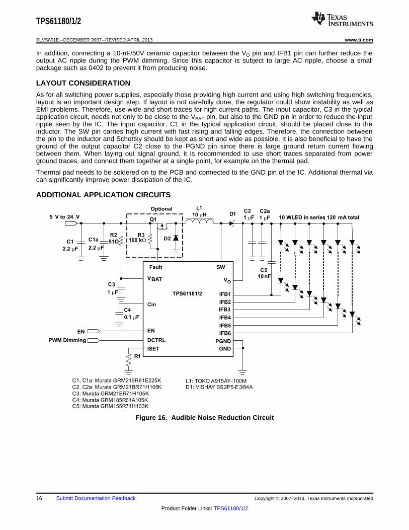
To further reduce the audible noise, one effective way is to use two or three small size capacitors in parallelinstead of one large capacitor. The application circuit in Figure 16 uses two 2.2-μF/25V ceramic capacitors at theinput and two 1-μF/50V ceramic capacitors at the output. All of the capacitors are in 0805 package. Although theoutput ripple during PWM dimming is higher than one 4.7μF in a 1206 package, the overall audible noise islower.
Copyright © 2007–2013, Texas Instruments Incorporated Submit Documentation Feedback 15
Product Folder Links: TPS61180/1/2
C2
1 Fm 10 WLED in series, 120 mA total
C510nF
C2aL1
10 HmQ1
D2
D1
IFB1
IFB2
IFB3
IFB4
IFB5
IFB6
VO
SWFault
VBAT
Cin
EN
DCTRL
ISET
PGND
GND
R1
TPS61181/2
C4
0.1 Fm
Optional
5 V to 24 V
C1a
EN
PWM Dimming
R2
51Ω
C3
1 Fm
C12.2 Fm
C1, C1a: Murata GRM219R61E225K
C2, C2a: Murata GRM21BR71H105K
C3: Murata GRM21BR71H105K
C4: Murata GRM185R61A105K
C5: Murata GRM155R71H103K
L1: TOKO A915AY-100M
D1: VISHAY SS2P5-E3/84A
R3100 kW
2.2 Fm
1 Fm
TPS61180/1/2
SLVS801E –DECEMBER 2007–REVISED APRIL 2013 www.ti.com
In addition, connecting a 10-nF/50V ceramic capacitor between the VO pin and IFB1 pin can further reduce theoutput AC ripple during the PWM dimming. Since this capacitor is subject to large AC ripple, choose a smallpackage such as 0402 to prevent it from producing noise.
LAYOUT CONSIDERATION
As for all switching power supplies, especially those providing high current and using high switching frequencies,layout is an important design step. If layout is not carefully done, the regulator could show instability as well asEMI problems. Therefore, use wide and short traces for high current paths. The input capacitor, C3 in the typicalapplication circuit, needs not only to be close to the VBAT pin, but also to the GND pin in order to reduce the inputripple seen by the IC. The input capacitor, C1 in the typical application circuit, should be placed close to theinductor. The SW pin carries high current with fast rising and falling edges. Therefore, the connection betweenthe pin to the inductor and Schottky should be kept as short and wide as possible. It is also beneficial to have theground of the output capacitor C2 close to the PGND pin since there is large ground return current flowingbetween them. When laying out signal ground, it is recommended to use short traces separated from powerground traces, and connect them together at a single point, for example on the thermal pad.
Thermal pad needs to be soldered on to the PCB and connected to the GND pin of the IC. Additional thermal viacan significantly improve power dissipation of the IC.
ADDITIONAL APPLICATION CIRCUITS
Figure 16. Audible Noise Reduction Circuit
16 Submit Documentation Feedback Copyright © 2007–2013, Texas Instruments Incorporated
Product Folder Links: TPS61180/1/2
L1
10 HmQ1
D2
D1C2
4.7 Fm
IFB1
IFB2
IFB3
IFB4
IFB5
IFB6
VO
SWFault
VBAT
Cin
EN
DCTRL
ISET
PGND
GND
R1
62 kW
TPS61180
C4
0.1uF
Optional
5 V to 24V
C1
4.7 Fm
10 WLED in series , 120 mA total
EN
PWM Dimming
3.3 V
R2
51Ω
C3
1 Fm
R3100 kW
L1
10 HmQ1
D2
D1 C24.7 Fm
IFB1
IFB2
IFB3
IFB4
IFB5
IFB6
VO
SWFault
VBAT
Cin
EN
DCTRL
ISET
PGND
GND
R1
62 kW
TPS61181/2
C40.1 Fm
Optional
5 V to 24 V
C14.7 Fm
10 WLED in series,120mA total
EN/PWM
R2
51Ω
C3
1 Fm
R3100 kW
TPS61180/1/2
www.ti.com SLVS801E –DECEMBER 2007–REVISED APRIL 2013
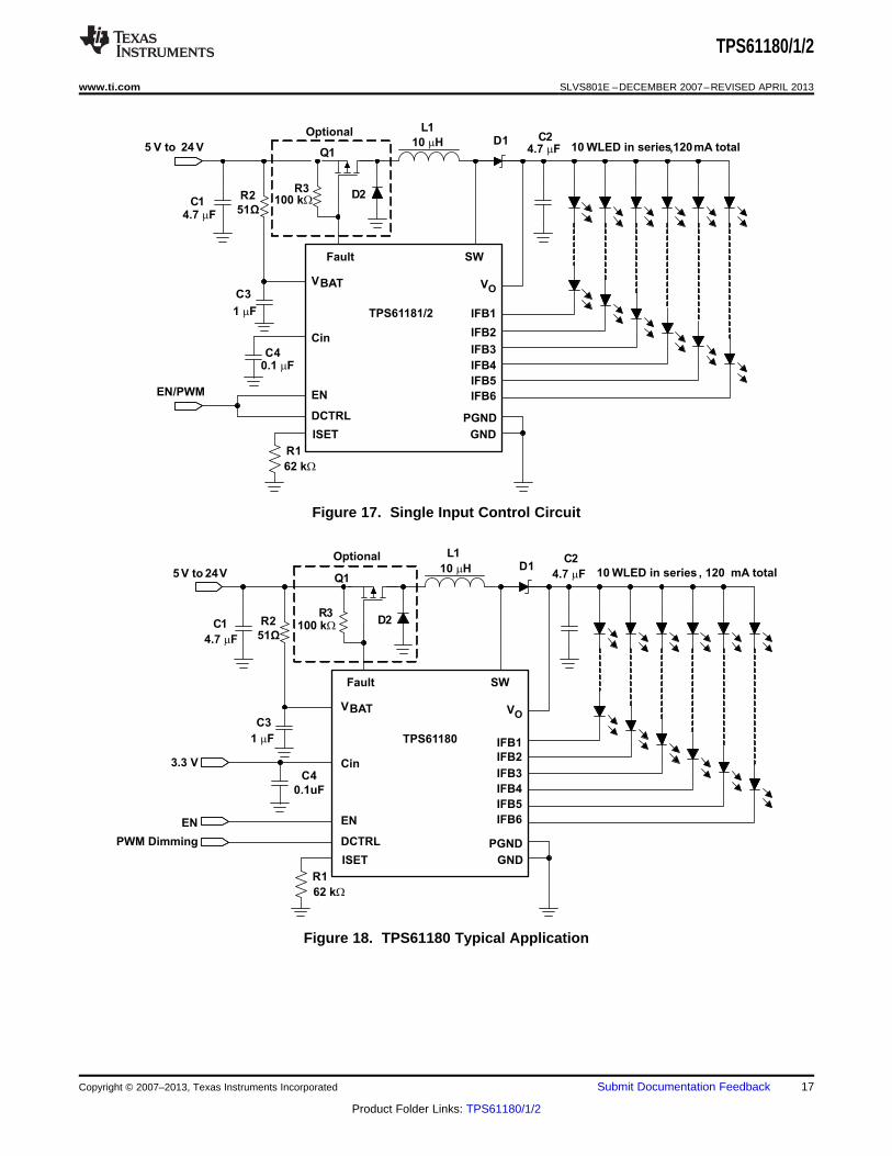
Figure 17. Single Input Control Circuit
Figure 18. TPS61180 Typical Application
Copyright © 2007–2013, Texas Instruments Incorporated Submit Documentation Feedback 17
Product Folder Links: TPS61180/1/2
IFB1
IFB2
IFB3
IFB4
IFB5
IFB6
VOVBAT
Cin
EN
DCTRL
ISET
PGND
GND
R1
62 kW
TPS61181/2
C3
1 Fm
C4
0.1 Fm
EN
PWM
S0334-01
L1
10 Hm D1
C2
4.7 Fm
SWFault
5 24 VV to
C1
4.7 Fm
10 WLEDs in Series40 mA Each String
R2
51 W
R3
100 kW
D2
Q1
Optional
L1
10 Hm D1
C2
4.7 Fm
IFB1
IFB2
IFB3
IFB4
IFB5
IFB6
VO
SWFault
VBAT
Cin
EN
DCTRL
ISET
PGND
GND
R1
62 kW
TPS61181/2
5 24 VV to
C1
4.7 Fm
C3
1 Fm
C4
0.1 Fm
10 WLEDs in Series20 mA Each String
EN
R2
51 W
R3
100 kW
D2
Q1
Optional
PWM
S0333-01
TPS61180/1/2
SLVS801E –DECEMBER 2007–REVISED APRIL 2013 www.ti.com
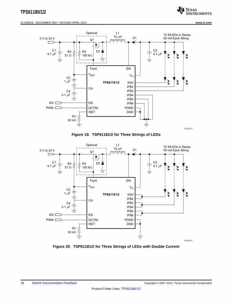
Figure 19. TSP61181/2 for Three Strings of LEDs
Figure 20. TSP61181/2 for Three Strings of LEDs with Double Current
18 Submit Documentation Feedback Copyright © 2007–2013, Texas Instruments Incorporated
Product Folder Links: TPS61180/1/2
IFB1
IFB2
IFB3
IFB4
IFB5
IFB6
VOVBAT
Cin
EN
DCTRL
ISET
PGND
GND
R1
62 kW
TPS61181/2
C3
1 Fm
C4
0.1 Fm
EN
PWM
10 WLEDs 120 mA
S0336-01
Hig
h-B
rightn
ess L
ED
L1
10 Hm D1
C2
4.7 Fm
SWFault
5 24 VV to
C1
4.7 FmR2
51 W
R3
100 kW
D2
Q1
Optional
IFB1
IFB2
IFB3
IFB4
IFB5
IFB6
VOVBAT
Cin
EN
DCTRL
ISET
PGND
GND
R1
51 kW
TPS61181/2
C3
1 Fm
C4
0.1 Fm
EN
PWM
S0335-01
Hig
h-B
rightn
ess L
ED
L1
10 Hm D1
C2
4.7 Fm
SWFault
5 24 VV to
C1
4.7 Fm
10 WLEDs in Series72 mA Each String
R2
51 W
R3
100 kW
D2
Q1
Optional
TPS61180/1/2
www.ti.com SLVS801E –DECEMBER 2007–REVISED APRIL 2013
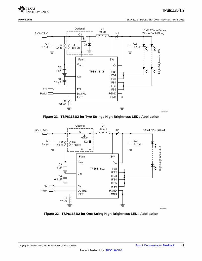
Figure 21. TSP61181/2 for Two Strings High Brightness LEDs Application
Figure 22. TSP61181/2 for One String High Brightness LEDs Application
Copyright © 2007–2013, Texas Instruments Incorporated Submit Documentation Feedback 19
Product Folder Links: TPS61180/1/2
TPS61180/1/2
SLVS801E –DECEMBER 2007–REVISED APRIL 2013 www.ti.com
REVISION HISTORY
Changes from Revision C (April 2009) to Revision D Page
• Added to ELEC CHARA table, sub section POWER SWITCH: first row, TEST CONDITIONS Col: VCC = 3.3 V forTPS61180 ............................................................................................................................................................................. 5
Changes from Revision D (February 2012) to Revision E Page
• Changed Dmin spec from 7% MAX to 8% for TPS61182 in Elec Char table. ....................................................................... 6
20 Submit Documentation Feedback Copyright © 2007–2013, Texas Instruments Incorporated
Product Folder Links: TPS61180/1/2
PACKAGE OPTION ADDENDUM
www.ti.com 24-Aug-2018
Addendum-Page 1
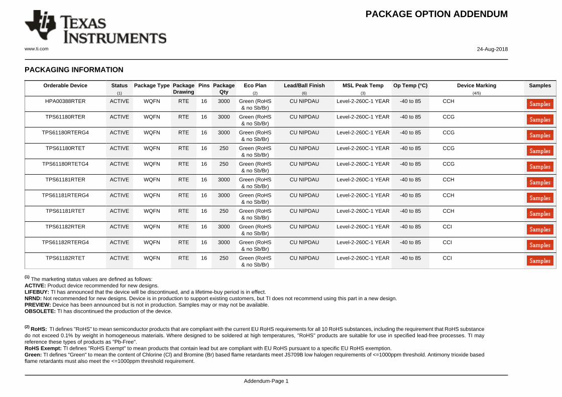
PACKAGING INFORMATION
Orderable Device Status(1)
Package Type PackageDrawing
Pins PackageQty
Eco Plan(2)
Lead/Ball Finish(6)
MSL Peak Temp(3)
Op Temp (°C) Device Marking(4/5)
Samples
HPA00388RTER ACTIVE WQFN RTE 16 3000 Green (RoHS& no Sb/Br)
CU NIPDAU Level-2-260C-1 YEAR -40 to 85 CCH
TPS61180RTER ACTIVE WQFN RTE 16 3000 Green (RoHS& no Sb/Br)
CU NIPDAU Level-2-260C-1 YEAR -40 to 85 CCG
TPS61180RTERG4 ACTIVE WQFN RTE 16 3000 Green (RoHS& no Sb/Br)
CU NIPDAU Level-2-260C-1 YEAR -40 to 85 CCG
TPS61180RTET ACTIVE WQFN RTE 16 250 Green (RoHS& no Sb/Br)
CU NIPDAU Level-2-260C-1 YEAR -40 to 85 CCG
TPS61180RTETG4 ACTIVE WQFN RTE 16 250 Green (RoHS& no Sb/Br)
CU NIPDAU Level-2-260C-1 YEAR -40 to 85 CCG
TPS61181RTER ACTIVE WQFN RTE 16 3000 Green (RoHS& no Sb/Br)
CU NIPDAU Level-2-260C-1 YEAR -40 to 85 CCH
TPS61181RTERG4 ACTIVE WQFN RTE 16 3000 Green (RoHS& no Sb/Br)
CU NIPDAU Level-2-260C-1 YEAR -40 to 85 CCH
TPS61181RTET ACTIVE WQFN RTE 16 250 Green (RoHS& no Sb/Br)
CU NIPDAU Level-2-260C-1 YEAR -40 to 85 CCH
TPS61182RTER ACTIVE WQFN RTE 16 3000 Green (RoHS& no Sb/Br)
CU NIPDAU Level-2-260C-1 YEAR -40 to 85 CCI
TPS61182RTERG4 ACTIVE WQFN RTE 16 3000 Green (RoHS& no Sb/Br)
CU NIPDAU Level-2-260C-1 YEAR -40 to 85 CCI
TPS61182RTET ACTIVE WQFN RTE 16 250 Green (RoHS& no Sb/Br)
CU NIPDAU Level-2-260C-1 YEAR -40 to 85 CCI
(1) The marketing status values are defined as follows:ACTIVE: Product device recommended for new designs.LIFEBUY: TI has announced that the device will be discontinued, and a lifetime-buy period is in effect.NRND: Not recommended for new designs. Device is in production to support existing customers, but TI does not recommend using this part in a new design.PREVIEW: Device has been announced but is not in production. Samples may or may not be available.OBSOLETE: TI has discontinued the production of the device.
(2) RoHS: TI defines "RoHS" to mean semiconductor products that are compliant with the current EU RoHS requirements for all 10 RoHS substances, including the requirement that RoHS substancedo not exceed 0.1% by weight in homogeneous materials. Where designed to be soldered at high temperatures, "RoHS" products are suitable for use in specified lead-free processes. TI mayreference these types of products as "Pb-Free".RoHS Exempt: TI defines "RoHS Exempt" to mean products that contain lead but are compliant with EU RoHS pursuant to a specific EU RoHS exemption.Green: TI defines "Green" to mean the content of Chlorine (Cl) and Bromine (Br) based flame retardants meet JS709B low halogen requirements of <=1000ppm threshold. Antimony trioxide basedflame retardants must also meet the <=1000ppm threshold requirement.
PACKAGE OPTION ADDENDUM
www.ti.com 24-Aug-2018
Addendum-Page 2
(3) MSL, Peak Temp. - The Moisture Sensitivity Level rating according to the JEDEC industry standard classifications, and peak solder temperature.
(4) There may be additional marking, which relates to the logo, the lot trace code information, or the environmental category on the device.
(5) Multiple Device Markings will be inside parentheses. Only one Device Marking contained in parentheses and separated by a "~" will appear on a device. If a line is indented then it is a continuationof the previous line and the two combined represent the entire Device Marking for that device.
(6) Lead/Ball Finish - Orderable Devices may have multiple material finish options. Finish options are separated by a vertical ruled line. Lead/Ball Finish values may wrap to two lines if the finishvalue exceeds the maximum column width.
Important Information and Disclaimer:The information provided on this page represents TI's knowledge and belief as of the date that it is provided. TI bases its knowledge and belief on informationprovided by third parties, and makes no representation or warranty as to the accuracy of such information. Efforts are underway to better integrate information from third parties. TI has taken andcontinues to take reasonable steps to provide representative and accurate information but may not have conducted destructive testing or chemical analysis on incoming materials and chemicals.TI and TI suppliers consider certain information to be proprietary, and thus CAS numbers and other limited information may not be available for release.
In no event shall TI's liability arising out of such information exceed the total purchase price of the TI part(s) at issue in this document sold by TI to Customer on an annual basis.
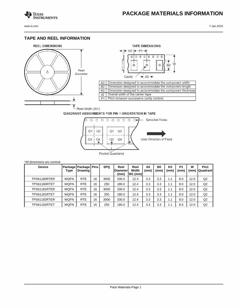
TAPE AND REEL INFORMATION
*All dimensions are nominal
Device PackageType
PackageDrawing
Pins SPQ ReelDiameter
(mm)
ReelWidth
W1 (mm)
A0(mm)
B0(mm)
K0(mm)
P1(mm)
W(mm)
Pin1Quadrant
TPS61180RTER WQFN RTE 16 3000 330.0 12.4 3.3 3.3 1.1 8.0 12.0 Q2
TPS61180RTET WQFN RTE 16 250 180.0 12.4 3.3 3.3 1.1 8.0 12.0 Q2
TPS61181RTER WQFN RTE 16 3000 330.0 12.4 3.3 3.3 1.1 8.0 12.0 Q2
TPS61181RTET WQFN RTE 16 250 180.0 12.4 3.3 3.3 1.1 8.0 12.0 Q2
TPS61182RTER WQFN RTE 16 3000 330.0 12.4 3.3 3.3 1.1 8.0 12.0 Q2
TPS61182RTET WQFN RTE 16 250 180.0 12.4 3.3 3.3 1.1 8.0 12.0 Q2
PACKAGE MATERIALS INFORMATION
www.ti.com 7-Jan-2015
Pack Materials-Page 1
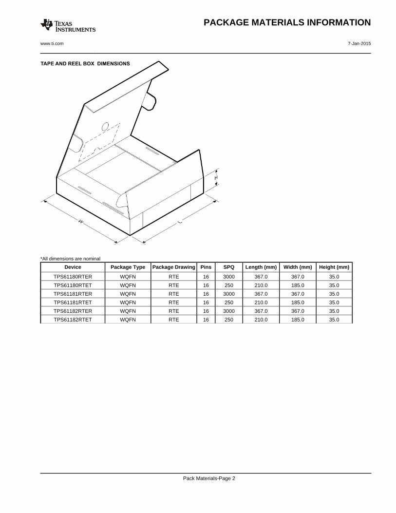
*All dimensions are nominal
Device Package Type Package Drawing Pins SPQ Length (mm) Width (mm) Height (mm)
TPS61180RTER WQFN RTE 16 3000 367.0 367.0 35.0
TPS61180RTET WQFN RTE 16 250 210.0 185.0 35.0
TPS61181RTER WQFN RTE 16 3000 367.0 367.0 35.0
TPS61181RTET WQFN RTE 16 250 210.0 185.0 35.0
TPS61182RTER WQFN RTE 16 3000 367.0 367.0 35.0
TPS61182RTET WQFN RTE 16 250 210.0 185.0 35.0
PACKAGE MATERIALS INFORMATION
www.ti.com 7-Jan-2015
Pack Materials-Page 2
IMPORTANT NOTICE
Texas Instruments Incorporated (TI) reserves the right to make corrections, enhancements, improvements and other changes to itssemiconductor products and services per JESD46, latest issue, and to discontinue any product or service per JESD48, latest issue. Buyersshould obtain the latest relevant information before placing orders and should verify that such information is current and complete.TI’s published terms of sale for semiconductor products (http://www.ti.com/sc/docs/stdterms.htm) apply to the sale of packaged integratedcircuit products that TI has qualified and released to market. Additional terms may apply to the use or sale of other types of TI products andservices.Reproduction of significant portions of TI information in TI data sheets is permissible only if reproduction is without alteration and isaccompanied by all associated warranties, conditions, limitations, and notices. TI is not responsible or liable for such reproduceddocumentation. Information of third parties may be subject to additional restrictions. Resale of TI products or services with statementsdifferent from or beyond the parameters stated by TI for that product or service voids all express and any implied warranties for theassociated TI product or service and is an unfair and deceptive business practice. TI is not responsible or liable for any such statements.Buyers and others who are developing systems that incorporate TI products (collectively, “Designers”) understand and agree that Designersremain responsible for using their independent analysis, evaluation and judgment in designing their applications and that Designers havefull and exclusive responsibility to assure the safety of Designers' applications and compliance of their applications (and of all TI productsused in or for Designers’ applications) with all applicable regulations, laws and other applicable requirements. Designer represents that, withrespect to their applications, Designer has all the necessary expertise to create and implement safeguards that (1) anticipate dangerousconsequences of failures, (2) monitor failures and their consequences, and (3) lessen the likelihood of failures that might cause harm andtake appropriate actions. Designer agrees that prior to using or distributing any applications that include TI products, Designer willthoroughly test such applications and the functionality of such TI products as used in such applications.TI’s provision of technical, application or other design advice, quality characterization, reliability data or other services or information,including, but not limited to, reference designs and materials relating to evaluation modules, (collectively, “TI Resources”) are intended toassist designers who are developing applications that incorporate TI products; by downloading, accessing or using TI Resources in anyway, Designer (individually or, if Designer is acting on behalf of a company, Designer’s company) agrees to use any particular TI Resourcesolely for this purpose and subject to the terms of this Notice.TI’s provision of TI Resources does not expand or otherwise alter TI’s applicable published warranties or warranty disclaimers for TIproducts, and no additional obligations or liabilities arise from TI providing such TI Resources. TI reserves the right to make corrections,enhancements, improvements and other changes to its TI Resources. TI has not conducted any testing other than that specificallydescribed in the published documentation for a particular TI Resource.Designer is authorized to use, copy and modify any individual TI Resource only in connection with the development of applications thatinclude the TI product(s) identified in such TI Resource. NO OTHER LICENSE, EXPRESS OR IMPLIED, BY ESTOPPEL OR OTHERWISETO ANY OTHER TI INTELLECTUAL PROPERTY RIGHT, AND NO LICENSE TO ANY TECHNOLOGY OR INTELLECTUAL PROPERTYRIGHT OF TI OR ANY THIRD PARTY IS GRANTED HEREIN, including but not limited to any patent right, copyright, mask work right, orother intellectual property right relating to any combination, machine, or process in which TI products or services are used. Informationregarding or referencing third-party products or services does not constitute a license to use such products or services, or a warranty orendorsement thereof. Use of TI Resources may require a license from a third party under the patents or other intellectual property of thethird party, or a license from TI under the patents or other intellectual property of TI.TI RESOURCES ARE PROVIDED “AS IS” AND WITH ALL FAULTS. TI DISCLAIMS ALL OTHER WARRANTIES ORREPRESENTATIONS, EXPRESS OR IMPLIED, REGARDING RESOURCES OR USE THEREOF, INCLUDING BUT NOT LIMITED TOACCURACY OR COMPLETENESS, TITLE, ANY EPIDEMIC FAILURE WARRANTY AND ANY IMPLIED WARRANTIES OFMERCHANTABILITY, FITNESS FOR A PARTICULAR PURPOSE, AND NON-INFRINGEMENT OF ANY THIRD PARTY INTELLECTUALPROPERTY RIGHTS. TI SHALL NOT BE LIABLE FOR AND SHALL NOT DEFEND OR INDEMNIFY DESIGNER AGAINST ANY CLAIM,INCLUDING BUT NOT LIMITED TO ANY INFRINGEMENT CLAIM THAT RELATES TO OR IS BASED ON ANY COMBINATION OFPRODUCTS EVEN IF DESCRIBED IN TI RESOURCES OR OTHERWISE. IN NO EVENT SHALL TI BE LIABLE FOR ANY ACTUAL,DIRECT, SPECIAL, COLLATERAL, INDIRECT, PUNITIVE, INCIDENTAL, CONSEQUENTIAL OR EXEMPLARY DAMAGES INCONNECTION WITH OR ARISING OUT OF TI RESOURCES OR USE THEREOF, AND REGARDLESS OF WHETHER TI HAS BEENADVISED OF THE POSSIBILITY OF SUCH DAMAGES.Unless TI has explicitly designated an individual product as meeting the requirements of a particular industry standard (e.g., ISO/TS 16949and ISO 26262), TI is not responsible for any failure to meet such industry standard requirements.Where TI specifically promotes products as facilitating functional safety or as compliant with industry functional safety standards, suchproducts are intended to help enable customers to design and create their own applications that meet applicable functional safety standardsand requirements. Using products in an application does not by itself establish any safety features in the application. Designers mustensure compliance with safety-related requirements and standards applicable to their applications. Designer may not use any TI products inlife-critical medical equipment unless authorized officers of the parties have executed a special contract specifically governing such use.Life-critical medical equipment is medical equipment where failure of such equipment would cause serious bodily injury or death (e.g., lifesupport, pacemakers, defibrillators, heart pumps, neurostimulators, and implantables). Such equipment includes, without limitation, allmedical devices identified by the U.S. Food and Drug Administration as Class III devices and equivalent classifications outside the U.S.TI may expressly designate certain products as completing a particular qualification (e.g., Q100, Military Grade, or Enhanced Product).Designers agree that it has the necessary expertise to select the product with the appropriate qualification designation for their applicationsand that proper product selection is at Designers’ own risk. Designers are solely responsible for compliance with all legal and regulatoryrequirements in connection with such selection.Designer will fully indemnify TI and its representatives against any damages, costs, losses, and/or liabilities arising out of Designer’s non-compliance with the terms and provisions of this Notice.
Mailing Address: Texas Instruments, Post Office Box 655303, Dallas, Texas 75265Copyright © 2018, Texas Instruments Incorporated