Embed Size (px)
Citation preview

TinyPowerTM A/D Type Smart Card OTP MCU
with DAC, ISO 7816 and USB Interfaces
HT56RB27
Revision: 1.20 Date: April 26, 2013
Table of Contents
Technical Document ...........................................................................7
Features ...............................................................................................7
General Description ............................................................................8
Block Diagram .....................................................................................8
Pin Assignment ...................................................................................9
Pin Description..................................................................................10
Absolute Maximum Ratings .............................................................12
D.C. Characteristics ..........................................................................13
A.C. Characteristics ..........................................................................15
A/D Converter Electrical Characteristics ........................................17
Power-on Reset Characteristics ......................................................17
DC/DC Converter and LDO Electrical Characteristics ...................18
System Architecture .........................................................................20Clocking and Pipelining ........................................................................................20
Program Counter..................................................................................................21
Stack ....................................................................................................................22
Arithmetic and Logic Unit � ALU...........................................................................22
Program Memory...............................................................................23Structure...............................................................................................................23
Special Vectors.....................................................................................................23
Look-up Table.......................................................................................................25
Table Program Example .....................................................................................25
Data Memory......................................................................................26Structure...............................................................................................................27
General Purpose Data Memory ............................................................................27
Special Purpose Data Memory .............................................................................27
Rev. 1.20 2 April 26, 2013
Contents
Special Function Registers Description .........................................29
Indirect Addressing Registers � IAR0, IAR1..........................................................29
Memory Pointers � MP0, MP1..............................................................................29
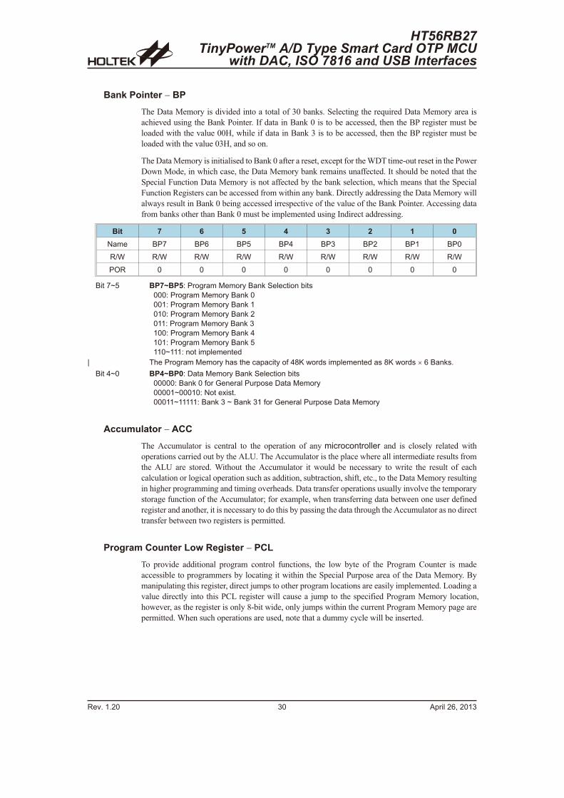
Bank Pointer � BP ................................................................................................30
Accumulator � ACC..............................................................................................30
Program Counter Low Register � PCL..................................................................30
Look-up Table Registers � TBLP, TBHP, TBLH.....................................................31
Status Register � STATUS ...................................................................................31
Interrupt Control Registers....................................................................................32
Timer/Event Counter Registers.............................................................................32
Input/Output Ports and Control Registers .............................................................32
Pulse Width Modulator Registers..........................................................................32
A/D Converter Registers � ADRL, ADRH, ADCR, ACSR......................................32
Serial Interface Module Registers.........................................................................33
Port A Wake-up Register � PAWU ........................................................................33
Pull-High Registers � PAPU, PBPU, PCPU ..........................................................33
Clock Control Register � CLKMOD.......................................................................33
Miscellaneous Register � MISC0, MISC1 .............................................................33
Input/Output Ports.............................................................................33Pull-high Resistors................................................................................................33
Port A Wake-up ....................................................................................................34
Port A Open Drain Function..................................................................................35
I/O Port Control Registers.....................................................................................35
Pin-shared Functions............................................................................................36
I/O Pin Structures .................................................................................................36
Programming Considerations ...............................................................................38
Timer/Event Counters .......................................................................38Configuring the Timer/Event Counter Input Clock Source.....................................38
Timer Registers � TMR0, TMR1L/TMR1H, TMR2, TMR3.....................................41
Configuring the Timer Mode .................................................................................41
Configuring the Event Counter Mode....................................................................42
Configuring the Pulse Width Measurement Mode.................................................42
Programmable Frequency Divider � PFD .............................................................43
Prescaler ..............................................................................................................44
I/O Interfacing.......................................................................................................44
Timer/Event Counter Pins Internal Filter ...............................................................44
Programming Considerations ...............................................................................45
Timer Program Example.......................................................................................46
Contents
Rev. 1.20 3 April 26, 2013
Pulse Width Modulator .....................................................................47PWM Overview ....................................................................................................47
8+4 PWM Mode Modulation .................................................................................48
PWM Output Control ............................................................................................48
PWM Register Pairs � PWMnH/PWMnL (n=0~3) .................................................49
PWM Programming Example ...............................................................................49
Analog to Digital Converter..............................................................50A/D Overview .......................................................................................................50
A/D Converter Data Registers � ADRL, ADRH.....................................................50
A/D Converter Control Registers � ADCR, ADPCR, ACSR ..................................51
A/D Operation.......................................................................................................52
A/D Input Pins ......................................................................................................53
Initialising the A/D Converter ................................................................................53
Programming Considerations ...............................................................................55
A/D Programming Example ..................................................................................55
A/D Transfer Function...........................................................................................57
Serial Interface Function � SIM........................................................58SPI Interface.........................................................................................................58
SPI Registers .......................................................................................................63
SPI Control Register � SIMnCTL2 ........................................................................64
SPI Communication..............................................................................................67
I2C Interface .........................................................................................................67
I2C Control Register � SIMAR...............................................................................69
I2C Bus Communication........................................................................................70
Peripheral Clock Output ...................................................................74Peripheral Clock Operation...................................................................................74
Buzzer.................................................................................................75PA0/PA1 Pin Function Control ..............................................................................75
Interrupts............................................................................................77Interrupt Registers ................................................................................................78
Interrupt Operation ...............................................................................................81
Interrupt Priority.....................................................................................................81
External Interrupt ..................................................................................................82
External Peripheral Interrupt .................................................................................83
Timer/Event Counter Interrupt ..............................................................................83
A/D Interrupt .........................................................................................................84
Smart Card Interrupt.............................................................................................84
Smart Card Insertion/Removal Interrupt ...............................................................84
SIM (SPI/I2C Interface) Interrupts .........................................................................84
Multi-function Interrupt ..........................................................................................85
Real Time Clock Interrupt .....................................................................................85
Time Base Interrupt ..............................................................................................86
Programming Considerations ...............................................................................87
Rev. 1.20 4 April 26, 2013
Contents
Reset and Initialisation .....................................................................88Reset Functions ...................................................................................................88
Reset Initial Conditions.........................................................................................90
Oscillator............................................................................................94System Clock Configurations................................................................................94
External Crystal/ Ceramic Oscillator � HXT .........................................................94
External RC Oscillator � ERC...............................................................................95
Internal RC Oscillator � HIRC...............................................................................95
Internal 32kHz RC Oscillator � LIRC.....................................................................95
External 32.768kHz Oscillator � LXT ....................................................................96
LXT Oscillator Low Power Function......................................................................97
External Oscillator � EC........................................................................................97
System Operating Modes .................................................................97Clock Sources ......................................................................................................97
.............................................................................................................................99
Operating Modes................................................................................................100
Power Down Mode and Wake-up ...................................................101Power Down Mode .............................................................................................101
Entering the Power Down Mode .........................................................................101
Standby Current Considerations.........................................................................101
Wake-up.............................................................................................................101
Low Voltage Detector � LVD...........................................................102LVD Operation....................................................................................................102
Watchdog Timer ..............................................................................103Watchdog Timer Operation.................................................................................103
Clearing the Watchdog Timer .............................................................................104
USB Interface...................................................................................105USB Operation ...................................................................................................105
USB Status and Control Registers......................................................................105
USB Register Summary .....................................................................................106
USB Interface Suspend Mode and Wake-up.......................................................114
USB Interrupt Structure......................................................................................115
Digital to Analog Converter � DAC ................................................116Operation............................................................................................................116
DC/DC Converter and LDO .............................................................117DC2DC Register.................................................................................................117
Contents
Rev. 1.20 5 April 26, 2013
Smart Card Interface .......................................................................118Interface Pins......................................................................................................118
Card Detection....................................................................................................118
Internal Time Counter � ETU, GTC, WTC...........................................................119
Elementary Time Unit � ETU ..............................................................................119
Guard Time Counter � GTC................................................................................120
Waiting Time Counter � WTC ............................................................................120
UART Interface...................................................................................................121
Power Control.....................................................................................................122
Smart Card Interrupt Structure............................................................................123
Programming Considerations .............................................................................124
Smart Card Interface Status and Control Registers ............................................124
Configuration Options ....................................................................133
Application Circuits ........................................................................135
Instruction Set .................................................................................136Introduction.........................................................................................................136
Instruction Timing ...............................................................................................136
Moving and Transferring Data ............................................................................136
Arithmetic Operations .........................................................................................136
Logical and Rotate Operations ...........................................................................136
Branches and Control Transfer...........................................................................137
Bit Operations.....................................................................................................137
Table Read Operations.......................................................................................137
Other Operations................................................................................................137
Instruction Set Summary ....................................................................................138
Instruction Definition ......................................................................140
Package Information.......................................................................150
SAW Type 40-pin QFN (6mm�6mm for 0.75mm) Outline Dimensions................151
44-pin LQFP (10mm�10mm) (FP2.0mm) Outline Dimensions............................152
Rev. 1.20 6 April 26, 2013
Contents
Technical Document
� Application Note
� HA0075E MCU Reset and Oscillator Circuits Application Note
Features
� Operating voltage:
fSYS=32.768kHz: 2.2V~5.5V
fSYS=4MHz: 2.2V~5.5V
fSYS=12MHz: 3.0V~5.5V
fSYS=20MHz: 4.5V~5.5V
� Operating current: fSYS=1MHz at 3V, 170�A, typ.
� OTP Program Memory: 48K�16
� RAM Data Memory: 3840�8
� 12 levels subroutine nesting
� Up to 24 bidirectional I/O lines
� TinyPower technology for low power operation
� Three pin-shared external interrupts lines
� Three 8-bit programmable Timer/Event Counters with overflow interrupt and 7-stage prescaler
� One 16-bit programmable Timer/Event Counters with overflow interrupt
� External Crystal (HXT), RC (ERC) and 32.768kHz (LXT) crystal oscillators
� Internal high speed RC oscillator - HIRC
� Fully integrated RC 32kHz oscillator - LIRC
� Externally supplied system clock option - EC
� Watchdog Timer function
� PFD/Buzzer for audio frequency generation
� Dual Serial Interface Modules (SIM): SPI and I2C
� 4 operating modes: Normal, Slow, Idle and Sleep
� 8-channel 12-bit resolution A/D converter
� 4-channel 12-bit PWM outputs
� 12-bit D/A converter with 8-level volume control
� USB interface
� Fully compliant with USB 1.1 full-speed specification
� Support 6 endpoints including endpoint 0
� Support Interrupt, Control and Bulk transfer
� 160 bytes total FIFO size - 8, 8, 8, 64, 8 and 64 bytes for endpoint0~endpoint 5 respectively
� Smartcard interface compatible with and certifiable to the ISO 7816-3 standards
� DC/DC converter and LDO function
� Low voltage reset function: 2.1V, 3.15V, 4.2V
� Low voltage detect function: 2.2V, 3.3V, 4.4V
� Bit manipulation instruction
� Table read instructions
� 63 powerful instructions
� Up to 0.2�s instruction cycle with 20MHz system clock at VDD=5V
� All instructions executed in one or two machine cycles
� Power down and wake-up functions to reduce power consumption
� Package type: 40-pin QFN and 44-pin LQFP
HT56RB27TinyPowerTM A/D Type Smart Card OTP MCUwith DAC, ISO 7816 and USB Interfaces
Rev. 1.20 7 April 26, 2013
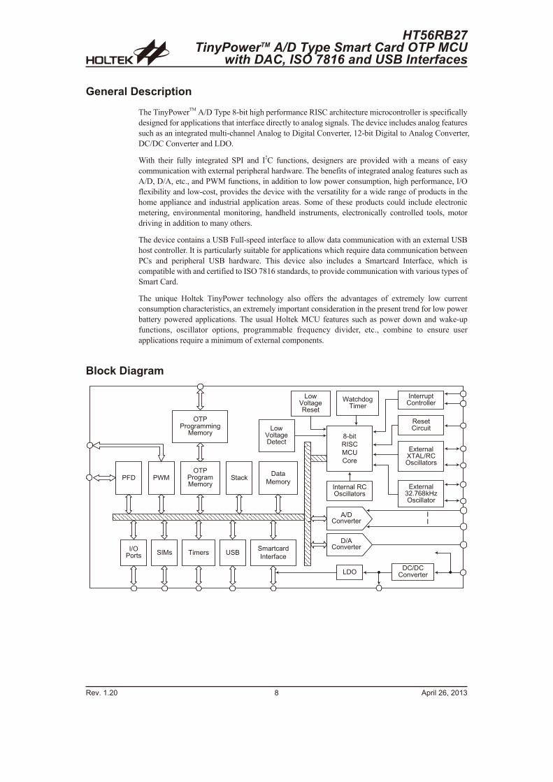
General Description
The TinyPowerTM
A/D Type 8-bit high performance RISC architecture microcontroller is specifically
designed for applications that interface directly to analog signals. The device includes analog features
such as an integrated multi-channel Analog to Digital Converter, 12-bit Digital to Analog Converter,
DC/DC Converter and LDO.
With their fully integrated SPI and I2C functions, designers are provided with a means of easy
communication with external peripheral hardware. The benefits of integrated analog features such as
A/D, D/A, etc., and PWM functions, in addition to low power consumption, high performance, I/O
flexibility and low-cost, provides the device with the versatility for a wide range of products in the
home appliance and industrial application areas. Some of these products could include electronic
metering, environmental monitoring, handheld instruments, electronically controlled tools, motor
driving in addition to many others.
The device contains a USB Full-speed interface to allow data communication with an external USB
host controller. It is particularly suitable for applications which require data communication between
PCs and peripheral USB hardware. This device also includes a Smartcard Interface, which is
compatible with and certified to ISO 7816 standards, to provide communication with various types of
Smart Card.
The unique Holtek TinyPower technology also offers the advantages of extremely low current
consumption characteristics, an extremely important consideration in the present trend for low power
battery powered applications. The usual Holtek MCU features such as power down and wake-up
functions, oscillator options, programmable frequency divider, etc., combine to ensure user
applications require a minimum of external components.
Block Diagram
Rev. 1.20 8 April 26, 2013
HT56RB27TinyPowerTM A/D Type Smart Card OTP MCU
with DAC, ISO 7816 and USB Interfaces
8-bitRISCMCUCore
WatchdogTimer
ResetCircuit
Internal RCOscillators
ExternalXTAL/RCOscillators
OTPProgramMemory
DataMemory
Stack
External32.768kHzOscillator
LowVoltageReset
InterruptController
LowVoltageDetect
D/AConverter
A/DConverter
OTPProgramming
Memory
SIMs Timers USBSmartcardInterface
I/OPorts
PFD PWM
DC/DCConverterLDO
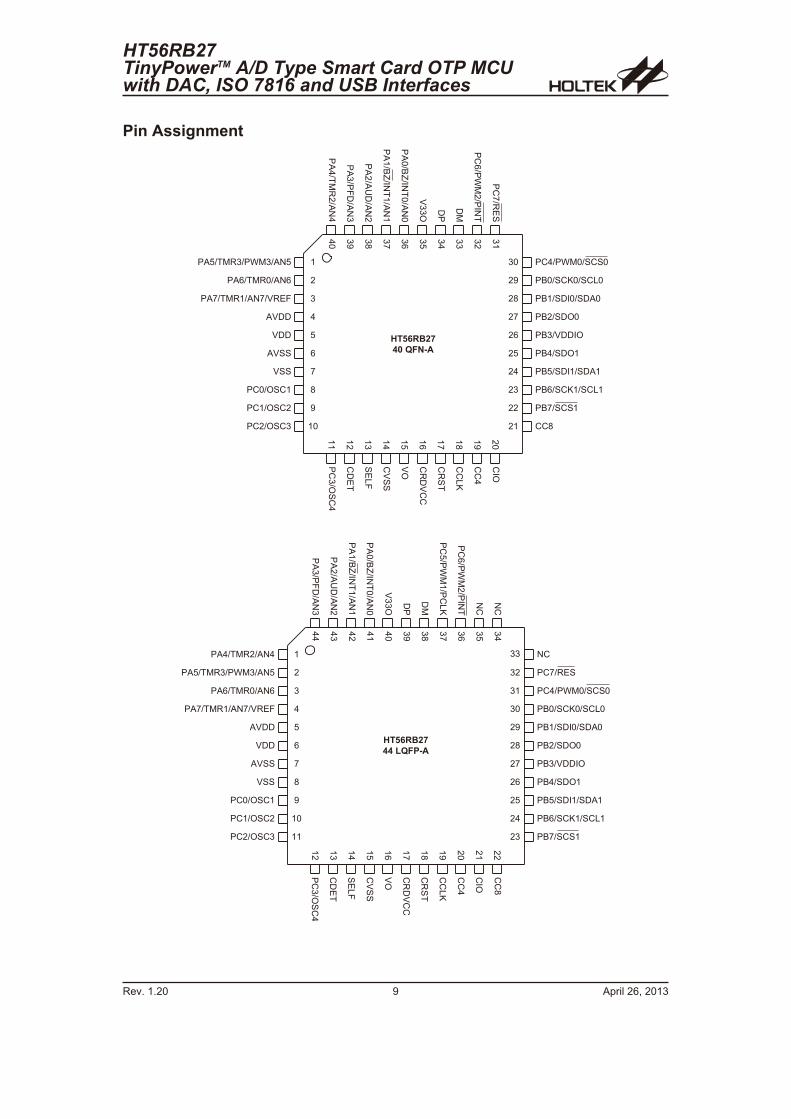
Pin Assignment
HT56RB27TinyPowerTM A/D Type Smart Card OTP MCUwith DAC, ISO 7816 and USB Interfaces
Rev. 1.20 9 April 26, 2013
2
3
4
5
6
7
8
9
10
11
12
13
14
15
16
17
18
19
20
21
22
23
24
25
26
27
28
29
30
31
32
1
HT56RB27
44 LQFP-A
44
43
42
41
40
39
38
37
36
35
34
33
PA
3/P
FD
/AN
3
PA
2/A
UD
/AN
2
PA
0/B
Z/IN
T0
/AN
0
PC7/RES
PC0/OSC1
PC1/OSC2
PC2/OSC3
PC
3/O
SC
4
V3
3O
DM
DP
PC
6/P
WM
2/P
INT
PC
5/P
WM
1/P
CL
K
PC4/PWM0/SCS0
PB0/SCK0/SCL0
PB1/SDI0/SDA0
PB2/SDO0
PB3/VDDIO
PB4/SDO1
PB5/SDI1/SDA1
PB7/SCS1
PB6/SCK1/SCL1
CR
DV
CC
CR
ST
CC
LK
CC
4
CIO
CC
8
CD
ET
PA
1/B
Z/IN
T1
/AN
1
AVSS
VSS
NC
PA4/TMR2/AN4
PA5/TMR3/PWM3/AN5
PA6/TMR0/AN6
PA7/TMR1/AN7/VREF
AVDD
NC
NC
VO
CV
SS
SE
LF
VDD
2
3
4
5
6
7
8
9
10
12
13
14
15
16
17
18
19
20
23
24
25
26
27
28
29
301
HT56RB27
40 QFN-A
40
39
38
37
36
35
34
PA
3/P
FD
/AN
3
PA
2/A
UD
/AN
2
PA
0/B
Z/IN
T0
/AN
0
PC
7/R
ES
PC0/OSC1
PC1/OSC2
PC2/OSC3
PC
3/O
SC
4
V3
3O
DM
DP
PC
6/P
WM
2/P
INT
PC4/PWM0/SCS0
PB0/SCK0/SCL0
PB1/SDI0/SDA0
PB2/SDO0
PB3/VDDIO
PB4/SDO1
PB5/SDI1/SDA1
PB7/SCS1
PB6/SCK1/SCL1
CR
DV
CC
CR
ST
CC
LK
CC
4
CIO
CC8
CD
ET
PA
1/B
Z/IN
T1
/AN
1
AVSS
VSS
PA
4/T
MR
2/A
N4
PA5/TMR3/PWM3/AN5
PA6/TMR0/AN6
PA7/TMR1/AN7/VREF
AVDD
VO
CV
SS
SE
LF
VDD3
3
32
31
22
21
11
Pin Description
The following table depicts the pins common to all devices.
Pin Name I/OConfiguration
OptionDescription
Input/Output
PA0/BZ/INT0/AN0
PA1/BZ/INT1/AN1
PA2/AUD/AN2
PA3/PFD/AN3
PA4/TMR2/AN4
PA5/TMR3/PWM3/AN5
PA6/TMR0/AN6
PA7/TMR1/AN7/VREF
I/OBZ/BZ
PFD
Bidirectional 8-bit input/output port. Each individual bit on this port
can be configured as a wake-up input by the PAWU register control
bit. Software instructions determine if the pin is a CMOS output or
Schmitt Trigger input. A pull-high resistor can be connected to each
pin determined by the PAPU register.
Port A is pin-shared with the A/D input pins. The A/D inputs are
selected via software instructions. Once a Port A line is selected as
an A/D input, the I/O function and pull-high resistor are disabled
automatically.
The BZ/INT0, BZ/INT1, PFD, TMR2, TMR3/PWM3, TMR0 and
TMR1 are pin-shared with PA0, PA1, PA3 and PA4~PA7
respectively.
AUD is the audio output pin from the D/A Converter and pin-shared
with PA2. When the D/A-Converter is enabled, the PA2 I/O function
will be disabled automatically, including any pull-high resistors. If the
D/A Converter output, AUD, and the A/D Converter input, AN2, are
both enabled, then the D/A converter output will be connected to the
AN2 input channel allowing the D/A output to be measured by the
A/D Converter.
VREF is the ADC reference voltage input pin. The �VREFS� bit in the
ACSR register is used to select either VREF or AVDD as the ADC
reference voltage.
PB0/SCK0/SCL0
PB1/SDI0/SDA0
PB2/SDO0
PB3/VDDIO *
PB4/SDO1
PB5/SDI1/SDA1
PB6/SCK1/SCL1
PB7/SCS1
I/O
VDDIO
SIM0
SIM1
Bidirectional 8-bit input/output port. Software instructions determine
if the pin is a CMOS output or Schmitt trigger input. A pull-high
resistor can be connected to each pin by the PBPU register.
SDO1, SDI1/SDA1, SCK1/SCL1 and SCS1 are the the SIM1
interface pins, pin-shared with PB4~PB7 respectively and enabled
by a configuration option, as well as the SIM0 interface pins. When
the configuration option enables the SIM function, the I/O function
will be disabled.
The VDDIO pin is an alternate power input pin for certain interface
functions, for example the 3.3V MXIC serial Flash Memory. It is
pin-shared with PB3. A Configuration option is used to determine if
PB3 is selected to be an I/O pin or the alternate power pin VDDIO.
When PB3 is selected as an alternate power pin, VDDIO, the power
supply of all the pins on this port, except PB3, together with PC4 can
be selected individually to come from the VDD pin or from VDDIO by
configuration options.
Rev. 1.20 10 April 26, 2013
HT56RB27TinyPowerTM A/D Type Smart Card OTP MCU
with DAC, ISO 7816 and USB Interfaces
Pin Name I/OConfiguration
OptionDescription
PC0/OSC1
PC1/OSC2
PC2/OSC3
PC3/OSC4
PC4/PWM0/SCS0
PC5/PWM1/PCLK
PC6/PWM2/PINT
I/O
ERC or HIRC
or EC
32.768kHz
SIM0
VDDIO
Bidirectional 7-bit input/output port. Software instructions determine
if the pin is a CMOS output or Schmitt trigger input. A pull-high
resistor can be connected to each pin determined by the PCPU
register.
OSC1 and OSC2 are connected to an external RC network or
crystal, determined by configuration options, for the internal system
clock. If the RC system clock option is selected, the OSC2 pin can be
used as an I/O pin. The internal system can come from the internal
high speed RC oscillator (HIRC) selected by configuration options.
When the HIRC is selected as the system oscillator, the OSC1 and
OSC2 pins can be used as normal I/O pins. The abbreviation EC
stands for External Clock mode. In the EC mode, an external clock
source is provided on OSC1 as the system clock.
OSC3 and OSC4 are connected to a 32.768kHz crystal oscillator to
form a clock source for fSUB or fSL.
PWM0, PWM1 and PWM2 are pin-shared with PC4, PC5 and PC6
respectively. PC4 is also pin-shared with SCS0, the chip select pin
for the Serial Interface Module 0. The power supply to PC4 can be
selected to come from VDD or VDDIO determined by a configuration
option.
The PCLK is a peripheral clock output pin which is enabled by the
�PCKEN� in the SIM0CTRL register and pin-shared with PC5.
The PINT is the external peripheral interrupt pin and pin-shared with
PC6.
PC7/RES I/O RES
Schmitt Trigger reset input pin, active low. The RES pin is pin-shared
with PC7 whose function is determined by a configuration option.
When PC7 is configured as an I/O pin, software instructions
determine if this pin is an open drain output or a Schmitt Trigger input
without pull-high resistor.
Power & Ground
VDD P � Positive power supply
VSS P � Negative power supply, ground
AVDD P � Analog positive power supply
AVSS P � Analog negative power supply, ground
CVSS P � DC/DC Converter Negative power supply, ground
USB
DP I/O � USB D+ line
DM I/O � USB D- line
V33O P � USB 3.3V regulator output
HT56RB27TinyPowerTM A/D Type Smart Card OTP MCUwith DAC, ISO 7816 and USB Interfaces
Rev. 1.20 11 April 26, 2013
Pin Name I/OConfiguration
OptionDescription
ISO 7816 - Smart Card Interface
VO P � External diode connection pin for DC/DC converter
SELF P � External inductor connection pin for DC/DC converter
CRST O � Smart card reset output
CCLK O � Smart card clock output
CC4 I/O � Smart card C4 input/output
CC8 I/O � Smart card C8 input/output
CIO I/O � Smart card data input/output
CDET I � Smart card detection input
CRDVCC P � Positive power supply for external smart card
Note: * For proper operation, VDDIO � VDD
Absolute Maximum Ratings
Supply Voltage ...............................................................................................VSS�0.3V to VSS+6.0V
Storage Temperature .................................................................................................�50C to 125C
Input Voltage .................................................................................................VSS�0.3V to VDD+0.3V
Operating Temperature................................................................................................�40C to 85C
IOL Total.....................................................................................................................................80mA
IOH Total ..................................................................................................................................�80mA
Total Power Dissipation .........................................................................................................500mW
Note: These are stress ratings only. Stresses exceeding the range specified under �Absolute Maximum Rat-
ings� may cause substantial damage to the device. Functional operation of this device at other condi-
tions beyond those listed in the specification is not implied and prolonged exposure to extreme
conditions may affect device reliability.
Rev. 1.20 12 April 26, 2013
HT56RB27TinyPowerTM A/D Type Smart Card OTP MCU
with DAC, ISO 7816 and USB Interfaces
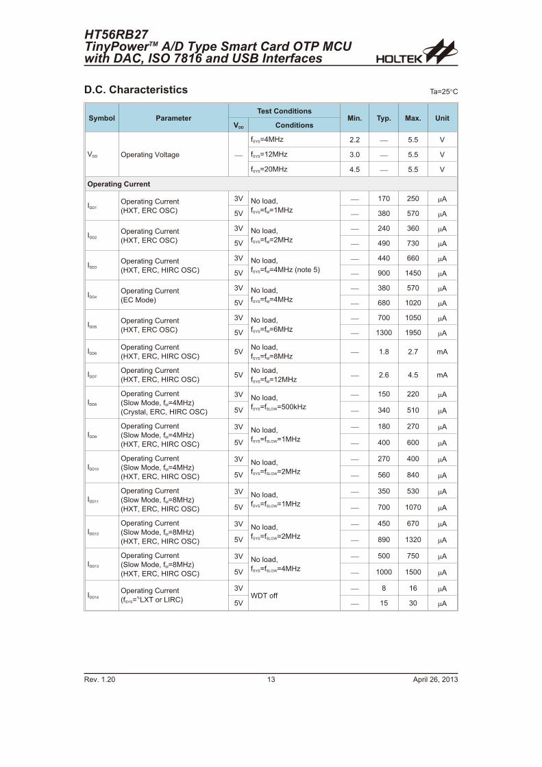
D.C. Characteristics Ta=25C
Symbol ParameterTest Conditions
Min. Typ. Max. UnitVDD Conditions
VDD Operating Voltage �
fSYS=4MHz 2.2 � 5.5 V
fSYS=12MHz 3.0 � 5.5 V
fSYS=20MHz 4.5 � 5.5 V
Operating Current
IDD1
Operating Current
(HXT, ERC OSC)
3V No load,
fSYS=fM=1MHz
� 170 250 �A
5V � 380 570 �A
IDD2
Operating Current
(HXT, ERC OSC)
3V No load,
fSYS=fM=2MHz
� 240 360 �A
5V � 490 730 �A
IDD3
Operating Current
(HXT, ERC, HIRC OSC)
3V No load,
fSYS=fM=4MHz (note 5)
� 440 660 �A
5V � 900 1450 �A
IDD4
Operating Current
(EC Mode)
3V No load,
fSYS=fM=4MHz
� 380 570 �A
5V � 680 1020 �A
IDD5
Operating Current
(HXT, ERC OSC)
3V No load,
fSYS=fM=6MHz
� 700 1050 �A
5V � 1300 1950 �A
IDD6
Operating Current
(HXT, ERC, HIRC OSC)5V
No load,
fSYS=fM=8MHz� 1.8 2.7 mA
IDD7
Operating Current
(HXT, ERC, HIRC OSC)5V
No load,
fSYS=fM=12MHz� 2.6 4.5 mA
IDD8
Operating Current
(Slow Mode, fM=4MHz)
(Crystal, ERC, HIRC OSC)
3V No load,
fSYS=fSLOW=500kHz
� 150 220 �A
5V � 340 510 �A
IDD9
Operating Current
(Slow Mode, fM=4MHz)
(HXT, ERC, HIRC OSC)
3V No load,
fSYS=fSLOW=1MHz
� 180 270 �A
5V � 400 600 �A
IDD10
Operating Current
(Slow Mode, fM=4MHz)
(HXT, ERC, HIRC OSC)
3V No load,
fSYS=fSLOW=2MHz
� 270 400 �A
5V � 560 840 �A
IDD11
Operating Current
(Slow Mode, fM=8MHz)
(HXT, ERC, HIRC OSC)
3V No load,
fSYS=fSLOW=1MHz
� 350 530 �A
5V � 700 1070 �A
IDD12
Operating Current
(Slow Mode, fM=8MHz)
(HXT, ERC, HIRC OSC)
3V No load,
fSYS=fSLOW=2MHz
� 450 670 �A
5V � 890 1320 �A
IDD13
Operating Current
(Slow Mode, fM=8MHz)
(HXT, ERC, HIRC OSC)
3V No load,
fSYS=fSLOW=4MHz
� 500 750 �A
5V � 1000 1500 �A
IDD14
Operating Current
(fSYS=%LXT or LIRC)
3VWDT off
� 8 16 �A
5V � 15 30 �A
HT56RB27TinyPowerTM A/D Type Smart Card OTP MCUwith DAC, ISO 7816 and USB Interfaces
Rev. 1.20 13 April 26, 2013
Symbol ParameterTest Conditions
Min. Typ. Max. UnitVDD Conditions
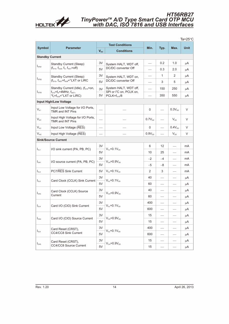
Standby Current
ISTB1
Standby Current (Sleep)
(fSYS, fSUB, fS, fWDT=off)
3V System HALT, WDT off,
DC/DC converter Off
� 0.2 1.0 �A
5V � 0.3 2.0 �A
ISTB2
Standby Current (Sleep)
(fSYS, fWDT=fSUB=%LXT or LIRC
3V System HALT, WDT on,
DC/DC converter Off
� 1 2 �A
5V � 3 5 �A
ISTB3
Standby Current (Idle), (fSYS=on,
fSYS=fM=4MHz, fWDT,
*fS=fSUB=%LXT or LIRC)
3V System HALT, WDT off,
SPI or I2C on, PCLK on,
PCLK=fSYS/8
� 150 250 �A
5V � 350 550 �A
Input High/Low Voltage
VIL1
Input Low Voltage for I/O Ports,
TMR and INT Pins� � 0 � 0.3VDD V
VIH1
Input High Voltage for I/O Ports,
TMR and INT Pins� � 0.7VDD � VDD V
VIL2 Input Low Voltage (RES) � � 0 � 0.4VDD V
VIH2 Input High Voltage (RES) � � 0.9VDD � VDD V
Sink/Source Current
IOL1 I/O sink current (PA, PB, PC)3V
VOL=0.1VDD
6 12 � mA
5V 10 25 � mA
IOH1 I/O source current (PA, PB, PC)3V
VOH=0.9VDD
�2 �4 � mA
5V �5 �8 � mA
IOL2 PC7/RES Sink Current 5V VOL=0.1VDD 2 3 � mA
IOL3 Card Clock (CCLK) Sink Current3V
VOL=0.1VDD
40 � � �A
5V 60 � � �A
IOH3
Card Clock (CCLK) Source
Current
3VVOH=0.9VDD
40 � � �A
5V 60 � � �A
IOL4 Card I/O (CIO) Sink Current3V
VOL=0.1VDD
400 � � �A
5V 600 � � �A
IOH4 Card I/O (CIO) Source Current3V
VOH=0.9VDD
15 � � �A
5V 15 � � �A
IOL5
Card Reset (CRST),
CC4/CC8 Sink Current
3VVOL=0.1VDD
400 � � �A
5V 600 � � �A
IOH5
Card Reset (CRST),
CC4/CC8 Source Current
3VVOH=0.9VDD
15 � � �A
5V 15 � � �A
Rev. 1.20 14 April 26, 2013
HT56RB27TinyPowerTM A/D Type Smart Card OTP MCU
with DAC, ISO 7816 and USB Interfaces
Ta=25C
Symbol ParameterTest Conditions
Min. Typ. Max. UnitVDD Conditions
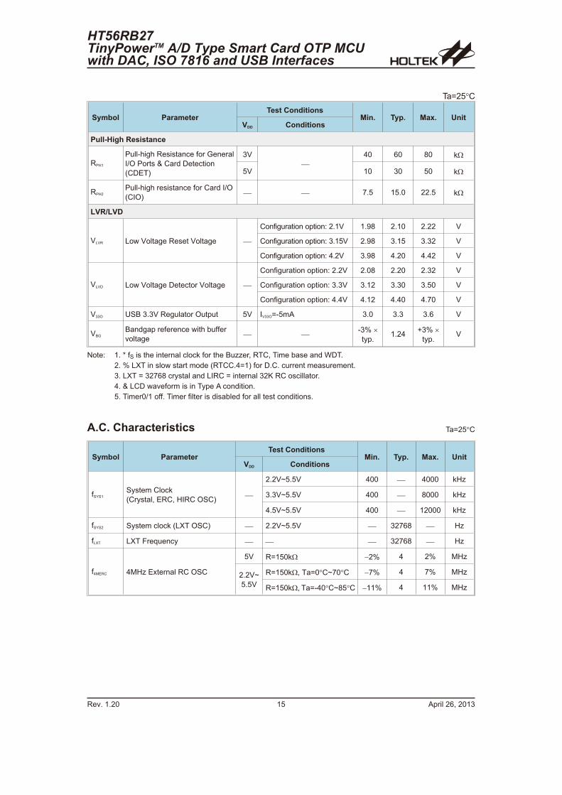
Pull-High Resistance
RPH1
Pull-high Resistance for General
I/O Ports & Card Detection
(CDET)
3V
�
40 60 80 k
5V 10 30 50 k
RPH2
Pull-high resistance for Card I/O
(CIO)� � 7.5 15.0 22.5 k
LVR/LVD
VLVR Low Voltage Reset Voltage �
Configuration option: 2.1V 1.98 2.10 2.22 V
Configuration option: 3.15V 2.98 3.15 3.32 V
Configuration option: 4.2V 3.98 4.20 4.42 V
VLVD Low Voltage Detector Voltage �
Configuration option: 2.2V 2.08 2.20 2.32 V
Configuration option: 3.3V 3.12 3.30 3.50 V
Configuration option: 4.4V 4.12 4.40 4.70 V
V33O USB 3.3V Regulator Output 5V IV33O=-5mA 3.0 3.3 3.6 V
VBG
Bandgap reference with buffer
voltage� �
-3% �
typ.1.24
+3% �
typ.V
Note: 1. * fS is the internal clock for the Buzzer, RTC, Time base and WDT.
2. % LXT in slow start mode (RTCC.4=1) for D.C. current measurement.
3. LXT = 32768 crystal and LIRC = internal 32K RC oscillator.
4. & LCD waveform is in Type A condition.
5. Timer0/1 off. Timer filter is disabled for all test conditions.
A.C. Characteristics Ta=25C
Symbol ParameterTest Conditions
Min. Typ. Max. UnitVDD Conditions
fSYS1
System Clock
(Crystal, ERC, HIRC OSC)�
2.2V~5.5V 400 � 4000 kHz
3.3V~5.5V 400 � 8000 kHz
4.5V~5.5V 400 � 12000 kHz
fSYS2 System clock (LXT OSC) � 2.2V~5.5V � 32768 � Hz
fLXT LXT Frequency � � � 32768 � Hz
f4MERC 4MHz External RC OSC
5V R=150k �2% 4 2% MHz
2.2V~
5.5V
R=150k, Ta=0C~70C �7% 4 7% MHz
R=150k, Ta=-40C~85C �11% 4 11% MHz
HT56RB27TinyPowerTM A/D Type Smart Card OTP MCUwith DAC, ISO 7816 and USB Interfaces
Rev. 1.20 15 April 26, 2013
Ta=25C
Symbol ParameterTest Conditions
Min. Typ. Max. UnitVDD Conditions
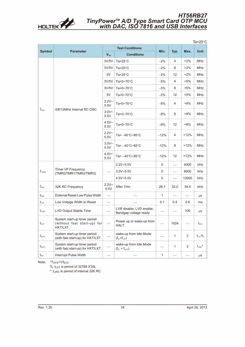
fHIRC 4/8/12MHz Internal RC OSC
3V/5V Ta=25C �2% 4 +2% MHz
3V/5V Ta=25C �2% 8 +2% MHz
5V Ta=25C �2% 12 +2% MHz
3V/5V Ta=0~70C �5% 4 +5% MHz
3V/5V Ta=0~70C �5% 8 +5% MHz
5V Ta=0~70C �5% 12 +5% MHz
2.2V~
5.5VTa=0~70C �8% 4 +8% MHz
3.0V~
5.5VTa=0~70C �8% 8 +8% MHz
4.5V~
5.5VTa=0~70C �8% 12 +8% MHz
2.2V~
5.5VTa= �40C~85C �12% 4 +12% MHz
3.0V~
5.5VTa= �40C~85C �12% 8 +12% MHz
4.5V~
5.5VTa= �40C~85C �12% 12 +12% MHz
fTIMER
Timer I/P Frequency
(TMR0/TMR1/TMR2/TMR3)�
2.2V~5.5V 0 � 4000 kHz
3.0V~5.5V 0 � 8000 kHz
4.5V~5.5V 0 � 12000 kHz
fLIRC 32K RC Frequency2.2V~
5.5VAfter Trim 28.1 32.0 34.4 kHz
tRES External Reset Low Pulse Width � � 1 � � �s
tLVR Low Voltage Width to Reset � � 0.1 0.4 0.6 ms
tLVDS LVD Output Stable Time �LVR disable, LVD enable,
Bandgap voltage ready� � 100 �s
tSST1
System start-up timer period
(without fast start-up) for
HXT/LXT�
Power up or wake-up from
HALT� 1024 � tSYS
tSST2
System start-up timer period
(with fast start-up) for HXT/LXT�
wake-up from Idle Mode
(fSL=fLXT)� 1 2 tLXT%
tSST3
System start-up timer period
(with fast start-up) for HXT/LXT�
wake-up from Idle Mode
(fSL = fLIRC)� 1 2 tLIRC*
tINT Interrupt Pulse Width � � 1 � � �s
Note: *TSYS=1/fSYS
%: tLXT is period of 32768 XTAL
*: tLIRC is period of internal 32K RC
Rev. 1.20 16 April 26, 2013
HT56RB27TinyPowerTM A/D Type Smart Card OTP MCU
with DAC, ISO 7816 and USB Interfaces
Ta=25C
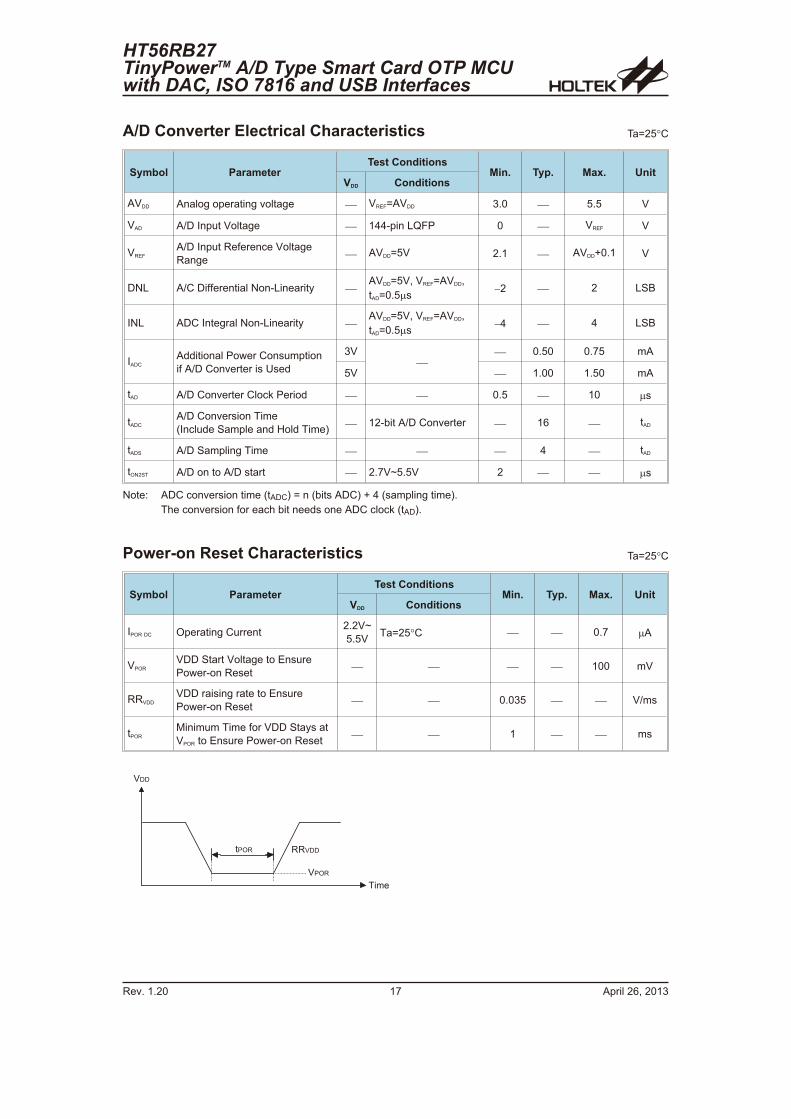
A/D Converter Electrical Characteristics Ta=25C
Symbol ParameterTest Conditions
Min. Typ. Max. UnitVDD Conditions
AVDD Analog operating voltage � VREF=AVDD 3.0 � 5.5 V
VAD A/D Input Voltage � 144-pin LQFP 0 � VREF V
VREF
A/D Input Reference Voltage
Range� AVDD=5V 2.1 � AVDD+0.1 V
DNL A/C Differential Non-Linearity �AVDD=5V, VREF=AVDD,
tAD=0.5�s�2 � 2 LSB
INL ADC Integral Non-Linearity �AVDD=5V, VREF=AVDD,
tAD=0.5�s�4 � 4 LSB
IADC
Additional Power Consumption
if A/D Converter is Used
3V�
� 0.50 0.75 mA
5V � 1.00 1.50 mA
tAD A/D Converter Clock Period � � 0.5 � 10 �s
tADC
A/D Conversion Time
(Include Sample and Hold Time)� 12-bit A/D Converter � 16 � tAD
tADS A/D Sampling Time � � � 4 � tAD
tON2ST A/D on to A/D start � 2.7V~5.5V 2 � � �s
Note: ADC conversion time (tADC) = n (bits ADC) + 4 (sampling time).
The conversion for each bit needs one ADC clock (tAD).
Power-on Reset Characteristics Ta=25C
Symbol ParameterTest Conditions
Min. Typ. Max. UnitVDD Conditions
IPOR DC Operating Current2.2V~
5.5VTa=25C � � 0.7 �A
VPOR
VDD Start Voltage to Ensure
Power-on Reset� � � � 100 mV
RRVDD
VDD raising rate to Ensure
Power-on Reset� � 0.035 � � V/ms
tPOR
Minimum Time for VDD Stays at
VPOR to Ensure Power-on Reset� � 1 � � ms
HT56RB27TinyPowerTM A/D Type Smart Card OTP MCUwith DAC, ISO 7816 and USB Interfaces
Rev. 1.20 17 April 26, 2013
� � � �
� � �
� �
� � �� �
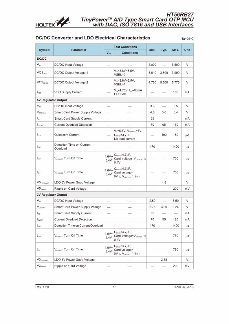
DC/DC Converter and LDO Electrical Characteristics Ta=25C
Symbol ParameterTest Conditions
Min. Typ. Max. UnitVDD Conditions
DC/DC
VIN DC/DC Input Voltage � � 3.000 � 5.500 V
VO1DC/DC DC/DC Output Voltage 1 �VIN=3.6V~5.5V,
VSEL=03.610 3.800 3.990 V
VO2DC/DC DC/DC Output Voltage 2 �VIN=3.6V~5.5V,
VSEL=14.750 5.500 5.775 V
IVDD VDD Supply Current �VIN=4.75V, ISC=60mA
CPU Idle� � 100 mA
5V Regulator Output
VIN DC/DC Input Voltage � � 3.6 � 5.5 V
VCRDVCC Smart Card Power Supply Voltage � � 4.6 5.0 5.4 V
ISC Smart Card Supply Current � � 55 � � mA
IOVDET Current Overload Detection � � 70 95 150 mA
IQUI Quiescent Current �
VO=5.5V, VCRDVCC=5V,
CLOAD=4.7�F,
No load current
� 100 150 �A
tIDET
Detection Time on Current
Overload� � 170 � 1400 �s
tOFF VCRDVCC Turn Off Time4.6V~
5.4V
CLOAD�4.7�F,
Card voltage=VCRDVCC to
0.4V
� � 750 �s
tON VCRDVCC Turn On Time4.6V~
5.4V
CLOAD�4.7�F,
Card voltage=
0V to VCRDVCC (min.)
� � 750 �s
V5PWRGOOD LDO 5V Power Good Voltage � � � 4.8 � V
V5RIPPLE Ripple on Card Voltage � � � � 200 mV
3V Regulator Output
VIN DC/DC Input Voltage � � 2.50 � 5.50 V
VCRDVCC Smart Card Power Supply Voltage � � 2.76 3.00 3.24 V
ISC Smart Card Supply Current � � 55 � � mA
IOVDET Current Overload Detection � � 70 95 120 mA
tIDET Detection Time on Current Overload � � 170 � 1400 �s
tOFF VCRDVCC Turn Off Time4.6V~
5.4V
CLOAD�4.7�F,
Card voltage=VCRDVCC to
0.4V
� � 750 �s
tON VCRDVCC Turn On Time4.6V~
5.4V
CLOAD�4.7�F,
Card voltage=
0V to VCRDVCC (min.)
� � 750 �s
V3PWRGOOD LDO 3V Power Good Voltage � � � 2.88 � V
V3RIPPLE Ripple on Card Voltage � � � � 200 mV
Rev. 1.20 18 April 26, 2013
HT56RB27TinyPowerTM A/D Type Smart Card OTP MCU
with DAC, ISO 7816 and USB Interfaces
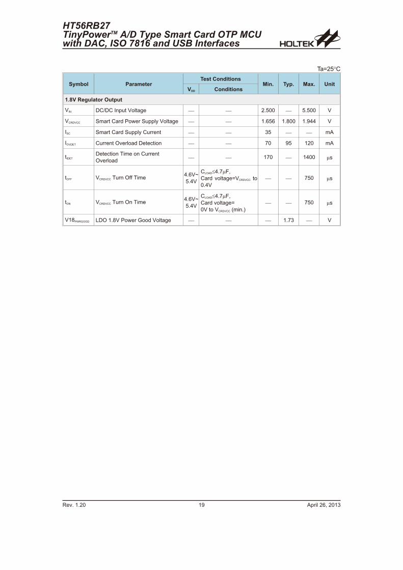
Symbol ParameterTest Conditions
Min. Typ. Max. UnitVDD Conditions
1.8V Regulator Output
VIN DC/DC Input Voltage � � 2.500 � 5.500 V
VCRDVCC Smart Card Power Supply Voltage � � 1.656 1.800 1.944 V
ISC Smart Card Supply Current � � 35 � � mA
IOVDET Current Overload Detection � � 70 95 120 mA
tIDET
Detection Time on Current
Overload� � 170 � 1400 �s
tOFF VCRDVCC Turn Off Time4.6V~
5.4V
CLOAD�4.7�F,
Card voltage=VCRDVCC to
0.4V
� � 750 �s
tON VCRDVCC Turn On Time4.6V~
5.4V
CLOAD�4.7�F,
Card voltage=
0V to VCRDVCC (min.)
� � 750 �s
V18PWRGOOD LDO 1.8V Power Good Voltage � � � 1.73 � V
HT56RB27TinyPowerTM A/D Type Smart Card OTP MCUwith DAC, ISO 7816 and USB Interfaces
Rev. 1.20 19 April 26, 2013
Ta=25C
System Architecture
A key factor in the high-performance features of the Holtek range of microcontrollers is attributed to
their internal system architecture. The range of devices take advantage of the usual features found
within RISC microcontrollers providing increased speed of operation and enhanced performance. The
pipelining scheme is implemented in such a way that instruction fetching and instruction execution are
overlapped, hence instructions are effectively executed in one cycle, with the exception of branch or
call instructions. An 8-bit wide ALU is used in practically all instruction set operations, which carries
out arithmetic operations, logic operations, rotation, increment, decrement, branch decisions, etc. The
internal data path is simplified by moving data through the Accumulator and the ALU. Certain internal
registers are implemented in the Data Memory and can be directly or indirectly addressed. The simple
addressing methods of these registers along with additional architectural features ensure that a
minimum of external components is required to provide a functional I/O and A/D control system with
maximum reliability and flexibility. This makes the device suitable for low-cost, high-volume
production for controller applications.
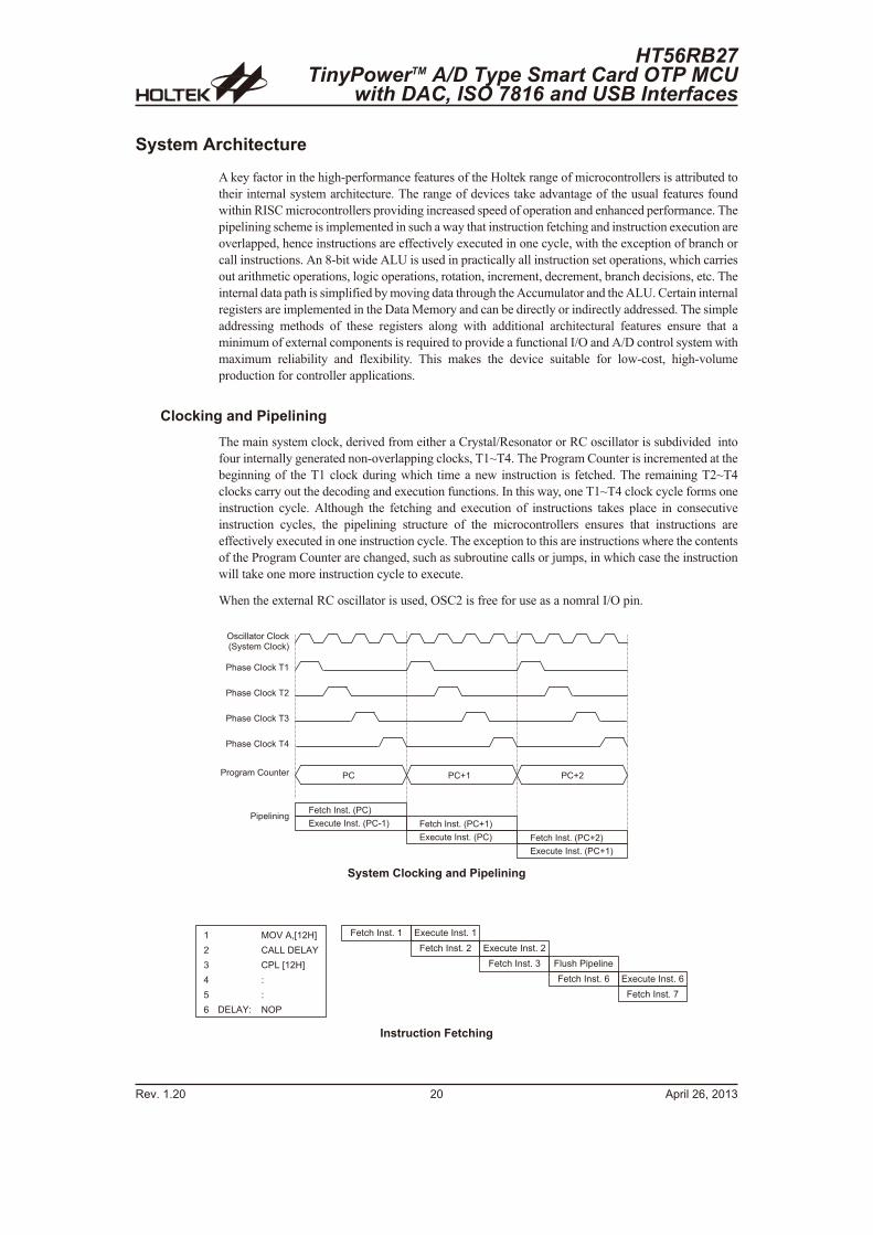
Clocking and Pipelining
The main system clock, derived from either a Crystal/Resonator or RC oscillator is subdivided into
four internally generated non-overlapping clocks, T1~T4. The Program Counter is incremented at the
beginning of the T1 clock during which time a new instruction is fetched. The remaining T2~T4
clocks carry out the decoding and execution functions. In this way, one T1~T4 clock cycle forms one
instruction cycle. Although the fetching and execution of instructions takes place in consecutive
instruction cycles, the pipelining structure of the microcontrollers ensures that instructions are
effectively executed in one instruction cycle. The exception to this are instructions where the contents
of the Program Counter are changed, such as subroutine calls or jumps, in which case the instruction
will take one more instruction cycle to execute.
When the external RC oscillator is used, OSC2 is free for use as a nomral I/O pin.
Rev. 1.20 20 April 26, 2013
HT56RB27TinyPowerTM A/D Type Smart Card OTP MCU
with DAC, ISO 7816 and USB Interfaces
� � � � � � � � � � � � � � �
� � � � � � � � � � � � � � � � � � � � � � � � � � � � � � � � � � � �
� � � � � � � � � � � � � � � � � � � � � � � � � � � � � � � � � �
� � � � � � � � � � � � � � � � � � �
� � � � � � � � � �
� � � � � � ! � � � "� # $ � � � � � � � " �
� � � � � � � � " � � �
� ! % ! � � � � � � � � !
� � � � � � � � " � � �
� � � � � � � � " � � &
� � � � � � � � " � � '
� � ( � � � � � � %
System Clocking and Pipelining
� � � � � � � � � � � � � � � � � � � � � � � � � �
� � � � � � � � � � � �
� � � � � � � � ( � � � � �
�
�
&
'
)
* � � + , - .
/ � � , 0 1 � � 2 3
� , + + � � � + , -
� � + � 1 � � 2 3
.
.
4 �
� � � � � � � � � � � � � �
� � � � � � � � � � � &
� � � � � � � � � � � * � � � � � � � � � � � � � *
� � � � � � � � � � � 5
Instruction Fetching
For instructions involving branches, such as jump or call instructions, two machine cycles are required
to complete instruction execution. An extra cycle is required as the program takes one cycle to first
obtain the actual jump or call address and then another cycle to actually execute the branch. The
requirement for this extra cycle should be taken into account by programmers in timing sensitive
applications.
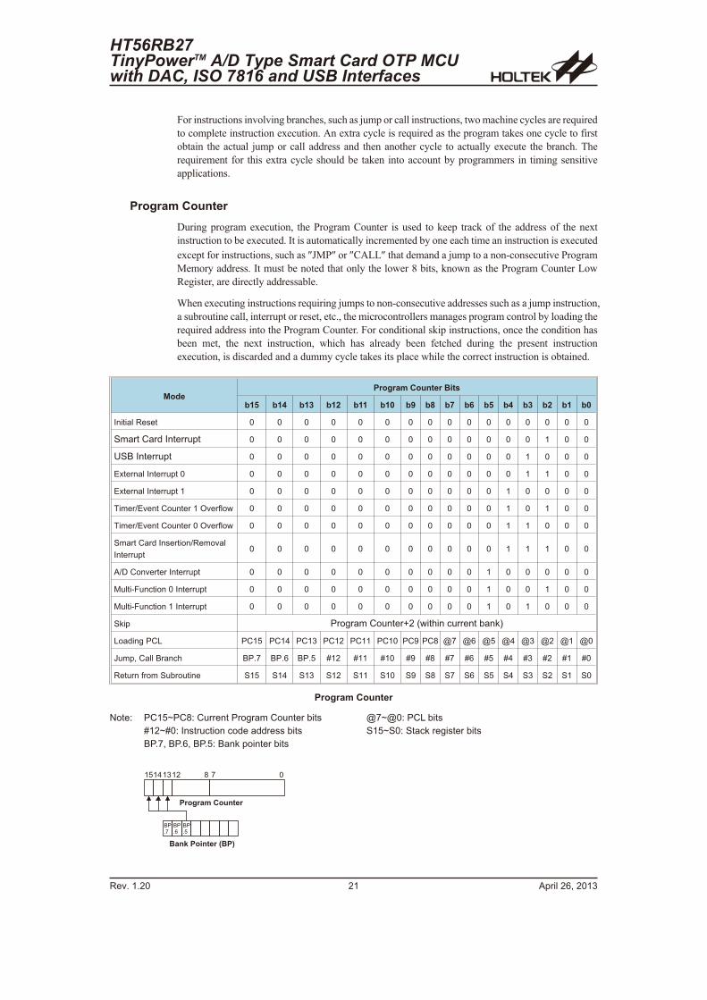
Program Counter
During program execution, the Program Counter is used to keep track of the address of the next
instruction to be executed. It is automatically incremented by one each time an instruction is executed
except for instructions, such as �JMP� or �CALL� that demand a jump to a non-consecutive Program
Memory address. It must be noted that only the lower 8 bits, known as the Program Counter Low
Register, are directly addressable.
When executing instructions requiring jumps to non-consecutive addresses such as a jump instruction,
a subroutine call, interrupt or reset, etc., the microcontrollers manages program control by loading the
required address into the Program Counter. For conditional skip instructions, once the condition has
been met, the next instruction, which has already been fetched during the present instruction
execution, is discarded and a dummy cycle takes its place while the correct instruction is obtained.
HT56RB27TinyPowerTM A/D Type Smart Card OTP MCUwith DAC, ISO 7816 and USB Interfaces
Rev. 1.20 21 April 26, 2013
ModeProgram Counter Bits
b15 b14 b13 b12 b11 b10 b9 b8 b7 b6 b5 b4 b3 b2 b1 b0
Initial Reset 0 0 0 0 0 0 0 0 0 0 0 0 0 0 0 0
Smart Card Interrupt 0 0 0 0 0 0 0 0 0 0 0 0 0 1 0 0
USB Interrupt 0 0 0 0 0 0 0 0 0 0 0 0 1 0 0 0
External Interrupt 0 0 0 0 0 0 0 0 0 0 0 0 0 1 1 0 0
External Interrupt 1 0 0 0 0 0 0 0 0 0 0 0 1 0 0 0 0
Timer/Event Counter 1 Overflow 0 0 0 0 0 0 0 0 0 0 0 1 0 1 0 0
Timer/Event Counter 0 Overflow 0 0 0 0 0 0 0 0 0 0 0 1 1 0 0 0
Smart Card Insertion/Removal
Interrupt0 0 0 0 0 0 0 0 0 0 0 1 1 1 0 0
A/D Converter Interrupt 0 0 0 0 0 0 0 0 0 0 1 0 0 0 0 0
Multi-Function 0 Interrupt 0 0 0 0 0 0 0 0 0 0 1 0 0 1 0 0
Multi-Function 1 Interrupt 0 0 0 0 0 0 0 0 0 0 1 0 1 0 0 0
Skip Program Counter+2 (within current bank)
Loading PCL PC15 PC14 PC13 PC12 PC11 PC10 PC9 PC8 @7 @6 @5 @4 @3 @2 @1 @0
Jump, Call Branch BP.7 BP.6 BP.5 #12 #11 #10 #9 #8 #7 #6 #5 #4 #3 #2 #1 #0
Return from Subroutine S15 S14 S13 S12 S11 S10 S9 S8 S7 S6 S5 S4 S3 S2 S1 S0
Program Counter
Note: PC15~PC8: Current Program Counter bits @7~@0: PCL bits
#12~#0: Instruction code address bits S15~S0: Stack register bits
BP.7, BP.6, BP.5: Bank pointer bits
� & � � 6 5 7
� � � � � � � � � � � �
8 �� )
� � � � � � � � � � � � � � � �
8 �� *
� '
8 �� 5
� )
The lower byte of the Program Counter, known as the Program Counter Low register or PCL, is
available for program control and is a readable and writable register. By transferring data directly into
this register, a short program jump can be executed directly, however, as only this low byte is available
for manipulation, the jumps are limited to the present page of memory, that is 256 locations. When such
program jumps are executed it should also be noted that a dummy cycle will be inserted.
The lower byte of the Program Counter is fully accessible under program control. Manipulating the
PCL might cause program branching, so an extra cycle is needed to pre-fetch. Further information on
the PCL register can be found in the Special Function Register section.
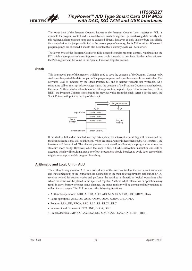
Stack
This is a special part of the memory which is used to save the contents of the Program Counter only.
And is neither part of the data nor part of the program space, and is neither readable nor writeable. The
activated level is indexed by the Stack Pointer, SP, and is neither readable nor writeable. At a
subroutine call or interrupt acknowledge signal, the contents of the Program Counter are pushed onto
the stack. At the end of a subroutine or an interrupt routine, signaled by a return instruction, RET or
RETI, the Program Counter is restored to its previous value from the stack. After a device reset, the
Stack Pointer will point to the top of the stack.
If the stack is full and an enabled interrupt takes place, the interrupt request flag will be recorded but
the acknowledge signal will be inhibited. When the Stack Pointer is decremented, by RET or RETI, the
interrupt will be serviced. This feature prevents stack overflow allowing the programmer to use the
structure more easily. However, when the stack is full, a CALL subroutine instruction can still be
executed which will result in a stack overflow. Precautions should be taken to avoid such cases which
might cause unpredictable program branching.
Arithmetic and Logic Unit � ALU
The arithmetic-logic unit or ALU is a critical area of the microcontrollers that carries out arithmetic
and logic operations of the instruction set. Connected to the main microcontrollers data bus, the ALU
receives related instruction codes and performs the required arithmetic or logical operations after
which the result will be placed in the specified register. As these ALU calculation or operations may
result in carry, borrow or other status changes, the status register will be correspondingly updated to
reflect these changes. The ALU supports the following functions:
� Arithmetic operations: ADD, ADDM, ADC, ADCM, SUB, SUBM, SBC, SBCM, DAA
� Logic operations: AND, OR, XOR, ANDM, ORM, XORM, CPL, CPLA
� Rotation RRA, RR, RRCA, RRC, RLA, RL, RLCA, RLC
� Increment and Decrement INCA, INC, DECA, DEC
� Branch decision, JMP, SZ, SZA, SNZ, SIZ, SDZ, SIZA, SDZA, CALL, RET, RETI
Rev. 1.20 22 April 26, 2013
HT56RB27TinyPowerTM A/D Type Smart Card OTP MCU
with DAC, ISO 7816 and USB Interfaces
� ! % ! � � � � � � � � !
# � � " � + � 9 � � � �
# � � " � + � 9 � � � �
# � � " � + � 9 � � � &
# � � " � + � 9 � � � � �
� ! % ! � �/ � � ! $
� ( � : � # � � "
# � � "� � � � � !
8 � � � � : � # � � "
Program Memory
The Program Memory is the location where the user code or program is stored. For the device the
Program Memory is an OTP type, which means it can be programmed only one time. By using the
appropriate programming tools, this OTP memory device offer users the flexibility to conveniently
debug and develop their applications while also offering a means of field programming.
Structure
The Program Memory has a capacity of 48K�16 bits. The Program Memory is addressed by the
Program Counter and also contains data, table information and interrupt-entries. Table data, which can
be setup in any location within the Program Memory, is addressed by a separate table pointer register.
Special Vectors
Within the Program Memory, certain locations are reserved for special usage such as reset and
interrupts.
� Location 000H
This vector is reserved for use by the device reset for program initialisation. After a device reset is
initiated, the program will jump to this location and begin execution.
� Location 004H
This vector is used by the Smart Card interrupt. If a related Smart Card interrupt event occurs, the
program will jump to this location and begin execution if the external interrupt is enabled and the
stack is not full.
� Location 008H
This vector is used by the USB interrupt. If the related USB interrupt event occurs, the program will
jump to this location and begin execution if the external interrupt is enabled and the stack is not full.
� Location 00CH
This vector is used by the external interrupt 0. If the related external interrupt pin receives an active
edge, the program will jump to this location and begin execution if the external interrupt is enabled
and the stack is not full.
� Location 010H
This vector is used by the external interrupt 1. If the related external interrupt pin receives an active
edge, the program will jump to this location and begin execution if the external interrupt is enabled
and the stack is not full.
� Location 014H
This internal vector is used by the Timer/Event Counter 0. If a Timer/Event Counter 0 overflow
occurs, the program will jump to this location and begin execution if the timer/event counter
interrupt is enabled and the stack is not full.
� Location 018H
This internal vector is used by the Timer/Event Counter 1. If a Timer/Event Counter 1 overflow
occurs, the program will jump to this location and begin execution if the timer/event counter
interrupt is enabled and the stack is not full.
� Location 01CH
This vector is used by the Smart Card Insertion/Removal interrupt. If a Smart Card Insertion or
Removal event occurs, the program will jump to this location and begin execution if the external
interrupt is enabled and the stack is not full.
HT56RB27TinyPowerTM A/D Type Smart Card OTP MCUwith DAC, ISO 7816 and USB Interfaces
Rev. 1.20 23 April 26, 2013
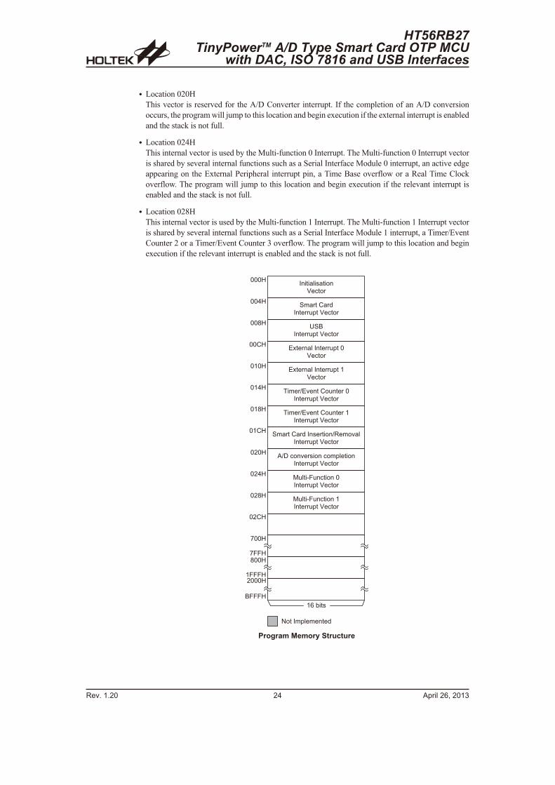
� Location 020H
This vector is reserved for the A/D Converter interrupt. If the completion of an A/D conversion
occurs, the program will jump to this location and begin execution if the external interrupt is enabled
and the stack is not full.
� Location 024H
This internal vector is used by the Multi-function 0 Interrupt. The Multi-function 0 Interrupt vector
is shared by several internal functions such as a Serial Interface Module 0 interrupt, an active edge
appearing on the External Peripheral interrupt pin, a Time Base overflow or a Real Time Clock
overflow. The program will jump to this location and begin execution if the relevant interrupt is
enabled and the stack is not full.
� Location 028H
This internal vector is used by the Multi-function 1 Interrupt. The Multi-function 1 Interrupt vector
is shared by several internal functions such as a Serial Interface Module 1 interrupt, a Timer/Event
Counter 2 or a Timer/Event Counter 3 overflow. The program will jump to this location and begin
execution if the relevant interrupt is enabled and the stack is not full.
Rev. 1.20 24 April 26, 2013
HT56RB27TinyPowerTM A/D Type Smart Card OTP MCU
with DAC, ISO 7816 and USB Interfaces
7 � ' 2
7 7 7 2
7 7 ' 2
7 7 6 2
7 7 � 2
7 � 7 2
7 � 6 2
4 � � � � ( � � � � � � � ;
8 � � � 2
� * � < � � �
� � � � � � � � � � � � �� � � !
# � � ! � � � � ! ;� � � � ! ! � ( � � � � � !
� � � � ! � � � � � � � � ! ! � ( � � 7� � � !
� � � � ! = � 9 � � � � � � � � � ! � 7� � � � ! ! � ( � � � � � !
> # 8� � � � ! ! � ( � � � � � !
� � � � ! � � � � � � � � ! ! � ( � � �� � � !
� � � � ! = � 9 � � � � � � � � � ! � �� � � � ! ! � ( � � � � � !
7 � � 2
5 7 7 2
5 � � 26 7 7 2
� � � � 2� 7 7 7 2
7 � ' 2
7 � 7 2
7 � 6 2
/ � � � � � � � � � � � � 7� � � � ! ! � ( � � � � � !
, = � � � 9 � ! � � � � � ( � � � � �� � � � ! ! � ( � � � � � !
/ � � � � � � � � � � � � �� � � � ! ! � ( � � � � � !
7 � � 2
# � � ! � � � � ! ; � � � � � ! � � � = � � 9 � �� � � � ! ! � ( � � � � � !
Program Memory Structure
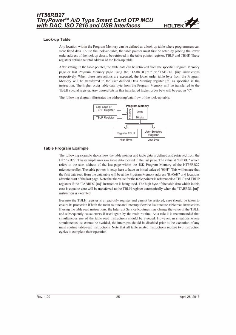
Look-up Table
Any location within the Program Memory can be defined as a look-up table where programmers can
store fixed data. To use the look-up table, the table pointer must first be setup by placing the lower
order address of the look up data to be retrieved in the table pointer register, TBLP and TBHP. These
registers define the total address of the look-up table.
After setting up the table pointer, the table data can be retrieved from the specific Program Memory
page or last Program Memory page using the �TABRDC[m]� or �TABRDL [m]� instructions,
respectively. When these instructions are executed, the lower order table byte from the Program
Memory will be transferred to the user defined Data Memory register [m] as specified in the
instruction. The higher order table data byte from the Program Memory will be transferred to the
TBLH special register. Any unused bits in this transferred higher order byte will be read as �0�.
The following diagram illustrates the addressing/data flow of the look-up table:
Table Program Example
The following example shows how the table pointer and table data is defined and retrieved from the
HT56RB27. This example uses raw table data located in the last page. The value at �BF00H� which
refers to the start address of the last page within the 48K Program Memory of the HT56RB27
microcontroller. The table pointer is setup here to have an initial value of �06H�. This will ensure that
the first data read from the data table will be at the Program Memory address �BF06H� or 6 locations
after the start of the last page. Note that the value for the table pointer is referenced to TBLP and TBHP
registers if the �TABRDC [m]� instruction is being used. The high byte of the table data which in this
case is equal to zero will be transferred to the TBLH register automatically when the �TABRDL [m]�
instruction is executed.
Because the TBLH register is a read-only register and cannot be restored, care should be taken to
ensure its protection if both the main routine and Interrupt Service Routine use table read instructions.
If using the table read instructions, the Interrupt Service Routines may change the value of the TBLH
and subsequently cause errors if used again by the main routine. As a rule it is recommended that
simultaneous use of the table read instructions should be avoided. However, in situations where
simultaneous use cannot be avoided, the interrupts should be disabled prior to the execution of any
main routine table-read instructions. Note that all table related instructions require two instruction
cycles to complete their operation.
HT56RB27TinyPowerTM A/D Type Smart Card OTP MCUwith DAC, ISO 7816 and USB Interfaces
Rev. 1.20 25 April 26, 2013
� % � � � � ! � � 8 + 2> � � ! � # � � � � � ;
� % � � � � !
2 � % � � 8 $ � � + ? � 8 $ � �
+ � � � � ( � % � � !� 8 2 � � � % � � � � !
� 8 + � � � % � � � � !
� � � �
,;;!��� � * � < � � �
� � � � � � � � � � � � �
rombank 5 code5
ds .section �data�Tempreg1 db ? ;temporaryregister#1tempreg2 db ? ;temporaryregister#2::code0 .section �code�mov a,06h ;initialise table pointer - note that this address
;is referencedmov tblp,a ;to the last page or the page that tbhp pointedmov a,0bfh ;initialise high table pointermov tbhp,a ;it is not necessary to set tbhp if executing tabrdl::tabrdc tempreg1tabrdl tempreg1 ;transfers value in table referenced by table pointer
;to tempregl;data at prog.memory address BF06H transferred to;tempreg1 and TBLH
dec tblp ;reduce value of table pointer by onetabrdc tempreg2tabrdl tempreg2 ;transfers value in table referenced by table pointer
;to tempreg2;data at prog.memory address BF05H transferred
to;tempreg2 and TBLH;in this example the data 1AH is transferred to;tempreg1 and data 0FH to tempreg2;the value 00H will be transferred to the high byte;register TBLH
::
code5 .section �code�org 1F00h ;sets initial address of lastpagedc 00Ah,00Bh,00Ch,00Dh,00Eh,00Fh,01Ah,01Bh
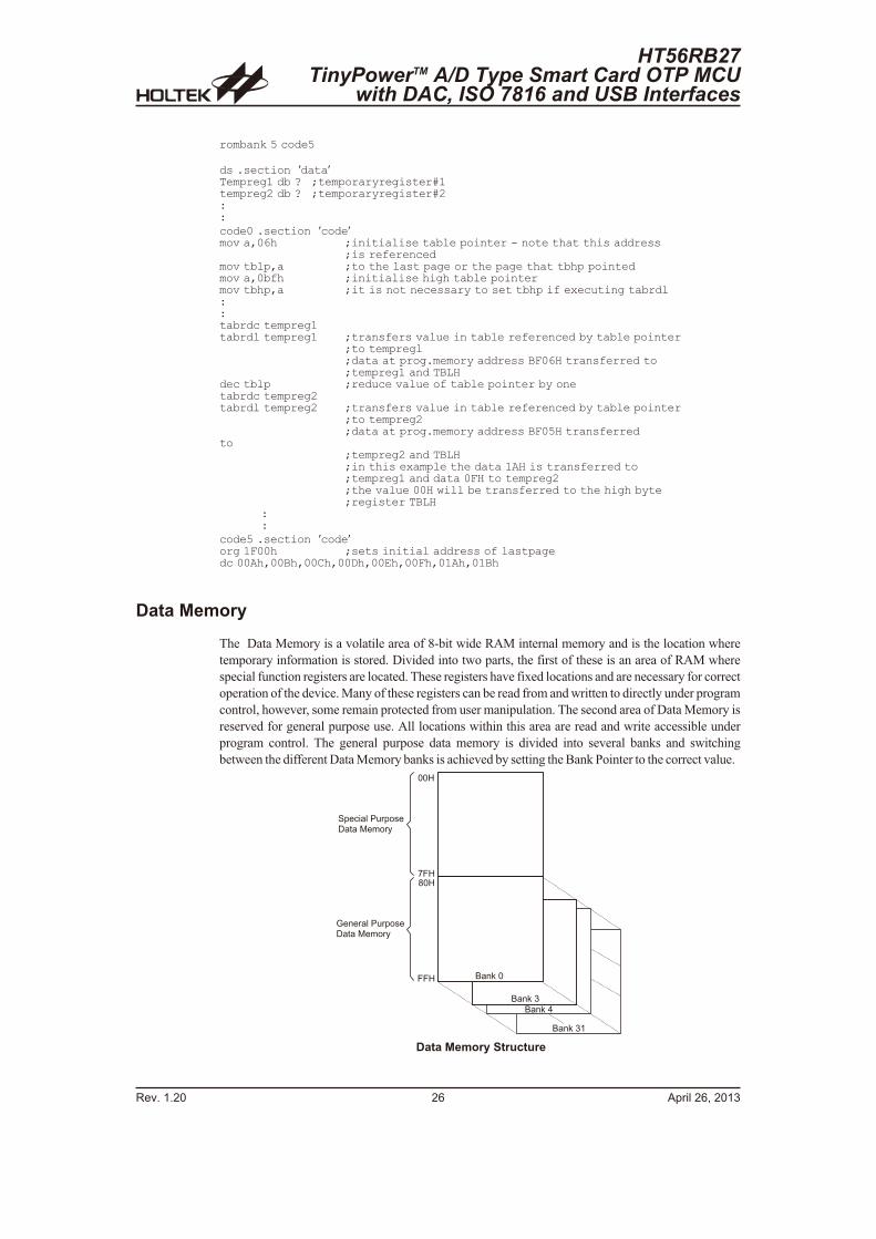
Data Memory
The Data Memory is a volatile area of 8-bit wide RAM internal memory and is the location where
temporary information is stored. Divided into two parts, the first of these is an area of RAM where
special function registers are located. These registers have fixed locations and are necessary for correct
operation of the device. Many of these registers can be read from and written to directly under program
control, however, some remain protected from user manipulation. The second area of Data Memory is
reserved for general purpose use. All locations within this area are read and write accessible under
program control. The general purpose data memory is divided into several banks and switching
between the different Data Memory banks is achieved by setting the Bank Pointer to the correct value.
Rev. 1.20 26 April 26, 2013
HT56RB27TinyPowerTM A/D Type Smart Card OTP MCU
with DAC, ISO 7816 and USB Interfaces
7 7 2
5 � 26 7 2
� � 2
# ( � � � � � � � ! ( � �� � � � � / � � ! $ �
@ � � � ! � � � � � ! ( � �� � � � � / � � ! $ �
8 � � " � 7 �
8 � � " � '
8 � � " � &
8 � � " � & �
Data Memory Structure
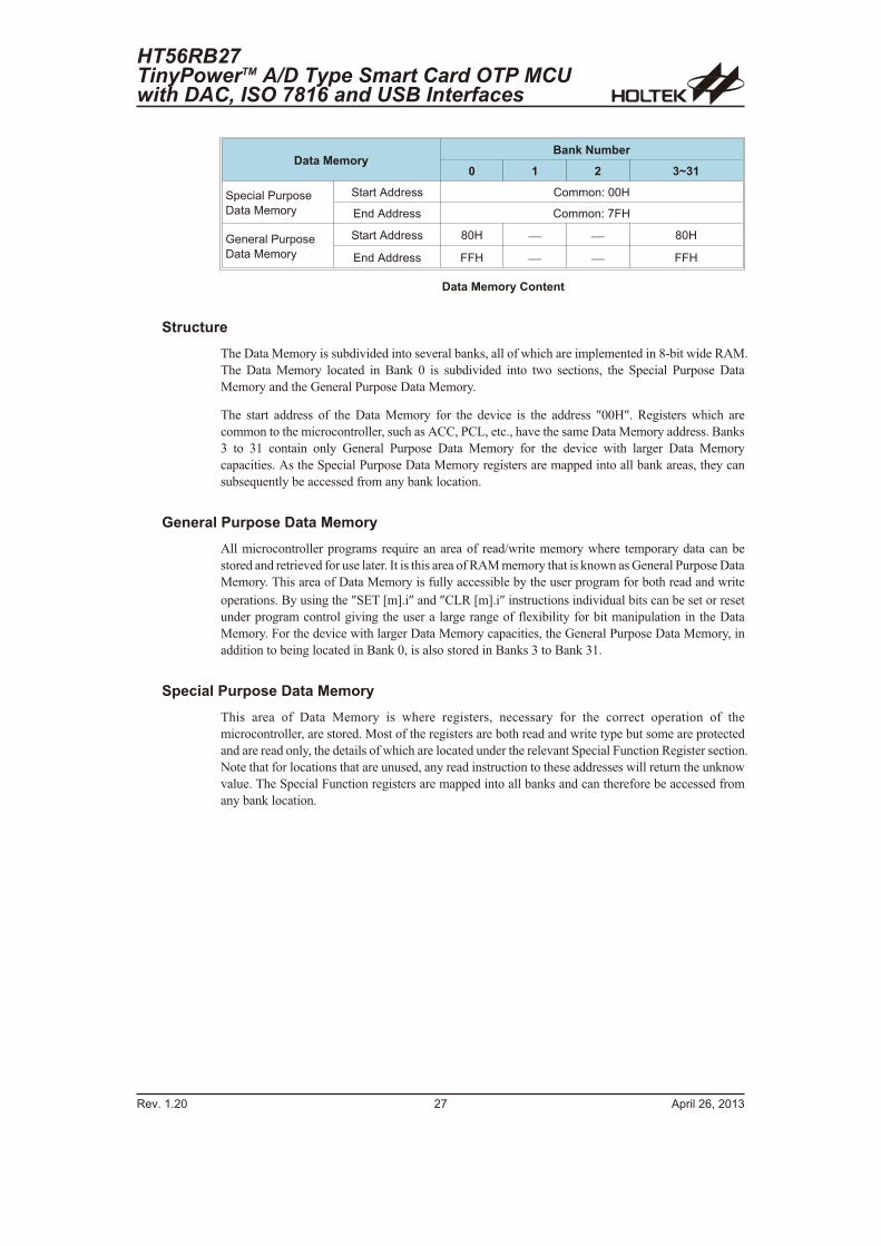
Data MemoryBank Number
0 1 2 3~31
Special Purpose
Data Memory
Start Address Common: 00H
End Address Common: 7FH
General Purpose
Data Memory
Start Address 80H � � 80H
End Address FFH � � FFH
Data Memory Content
Structure
The Data Memory is subdivided into several banks, all of which are implemented in 8-bit wide RAM.
The Data Memory located in Bank 0 is subdivided into two sections, the Special Purpose Data
Memory and the General Purpose Data Memory.
The start address of the Data Memory for the device is the address �00H�. Registers which are
common to the microcontroller, such as ACC, PCL, etc., have the same Data Memory address. Banks
3 to 31 contain only General Purpose Data Memory for the device with larger Data Memory
capacities. As the Special Purpose Data Memory registers are mapped into all bank areas, they can
subsequently be accessed from any bank location.
General Purpose Data Memory
All microcontroller programs require an area of read/write memory where temporary data can be
stored and retrieved for use later. It is this area of RAM memory that is known as General Purpose Data
Memory. This area of Data Memory is fully accessible by the user program for both read and write
operations. By using the �SET [m].i� and �CLR [m].i� instructions individual bits can be set or reset
under program control giving the user a large range of flexibility for bit manipulation in the Data
Memory. For the device with larger Data Memory capacities, the General Purpose Data Memory, in
addition to being located in Bank 0, is also stored in Banks 3 to Bank 31.
Special Purpose Data Memory
This area of Data Memory is where registers, necessary for the correct operation of the
microcontroller, are stored. Most of the registers are both read and write type but some are protected
and are read only, the details of which are located under the relevant Special Function Register section.
Note that for locations that are unused, any read instruction to these addresses will return the unknow
value. The Special Function registers are mapped into all banks and can therefore be accessed from
any bank location.
HT56RB27TinyPowerTM A/D Type Smart Card OTP MCUwith DAC, ISO 7816 and USB Interfaces
Rev. 1.20 27 April 26, 2013
Rev. 1.20 28 April 26, 2013
HT56RB27TinyPowerTM A/D Type Smart Card OTP MCU
with DAC, ISO 7816 and USB Interfaces
7 7 2
7 � 2
7 � 2
7 & 2
7 ' 2
7 ) 2
7 * 2
7 5 2
7 6 2
7 A 2
7 , 2
7 8 2
7 � 2
7 � 2
7 � 2
7 � 2
� 7 2
� � 2
� � 2
� & 2
� ' 2
� ) 2
� * 2
� 5 2
� 6 2
� A 2
� , 2
� 8 2
� � 2
� � 2
� � 2
� � 2
� 7 2
� � 2
� � 2
� & 2
� ' 2
� ) 2
� * 2
� 5 2
� 6 2
� A 2
� , 2
� 8 2
� � 2
� � 2
� � 2
� � 2
& 7 2
& � 2
& � 2
& & 2
& ' 2
& ) 2
& * 2
& 5 2
& 6 2
& A 2
& , 2
& 8 2
& � 2
& � 2
& � 2
& � 2
� , 7
/ � 7
� , �
/ � �
8 �
, � �
� � +
� 8 + �
� 8 + 2
� � �
# � , � > #
� 8 2 �
/ � # � 7
/ � # � �
� + B / �
� � � � �
� 4 � � 7
� 4 � � �
� 4 � � �
/ � � � 7
/ � � � �
� , C >
� , � >
� ,
� , �
� 8 � >
� 8
� 8 �
� � � >
� �
� � �
� C / 7 +
� C / 7 2
� C / � +
� C / � 2
� C / � +
� C / � 2
� C / & +
� C / & 2
� / 7
� / 7 �
� / � 2
� / � +
� / � �
� / �
� / � �
� / &
� / & �
� � + �
, � +
, � 2
, � �
, � #
, � � �
# � / 7 � � + 7
# � / 7 � � + �
# � / 7 �
# � / 7 , = # � / 7 � � + �
# � / � � � + 7
# � / � � � + �
# � / � �
# � / � , = # � / � � � + �
� , +
� , 2
� , � � +
� �
� #
� � �
� � � > �
� � � > 7
� @ � �
� @ � 7
� C � �
� C � �
� C � 7
� � �
� � �
� � D 8
� D 8
> # �
> #
> � �
, C
# � , + +
# � � #
> / � # �
# � � �
� � � 7
� � � �
� � � �
� � � &
� � � '
� � � )
> � �
4 � � /
� � � �
' 7 2
' � 2
' � 2
' & 2
' ' 2
' ) 2
' * 2
' 5 2
' 6 2
' A 2
' , 2
' 8 2
' � 2
' � 2
' � 2
' � 2
) 7 2
) � 2
) � 2
) & 2
) ' 2
) ) 2
) * 2
) 5 2
) 6 2
) A 2
) , 2
) 8 2
) � 2
) � 2
) � 2
) � 2
* 7 2
* � 2
* � 2
* & 2
* ' 2
* ) 2
* * 2
* 5 2
* 6 2
* A 2
* , 2
* 8 2
* � 2
* � 2
* � 2
* � 2
5 7 2
5 � 2
5 � 2
5 & 2
5 ' 2
5 ) 2
5 * 2
5 5 2
5 6 2
5 A 2
5 , 2
5 8 2
5 � 2
5 � 2
5 � 2
5 � 2
. � > � � � � ; � � � ; � � � � E D D E �
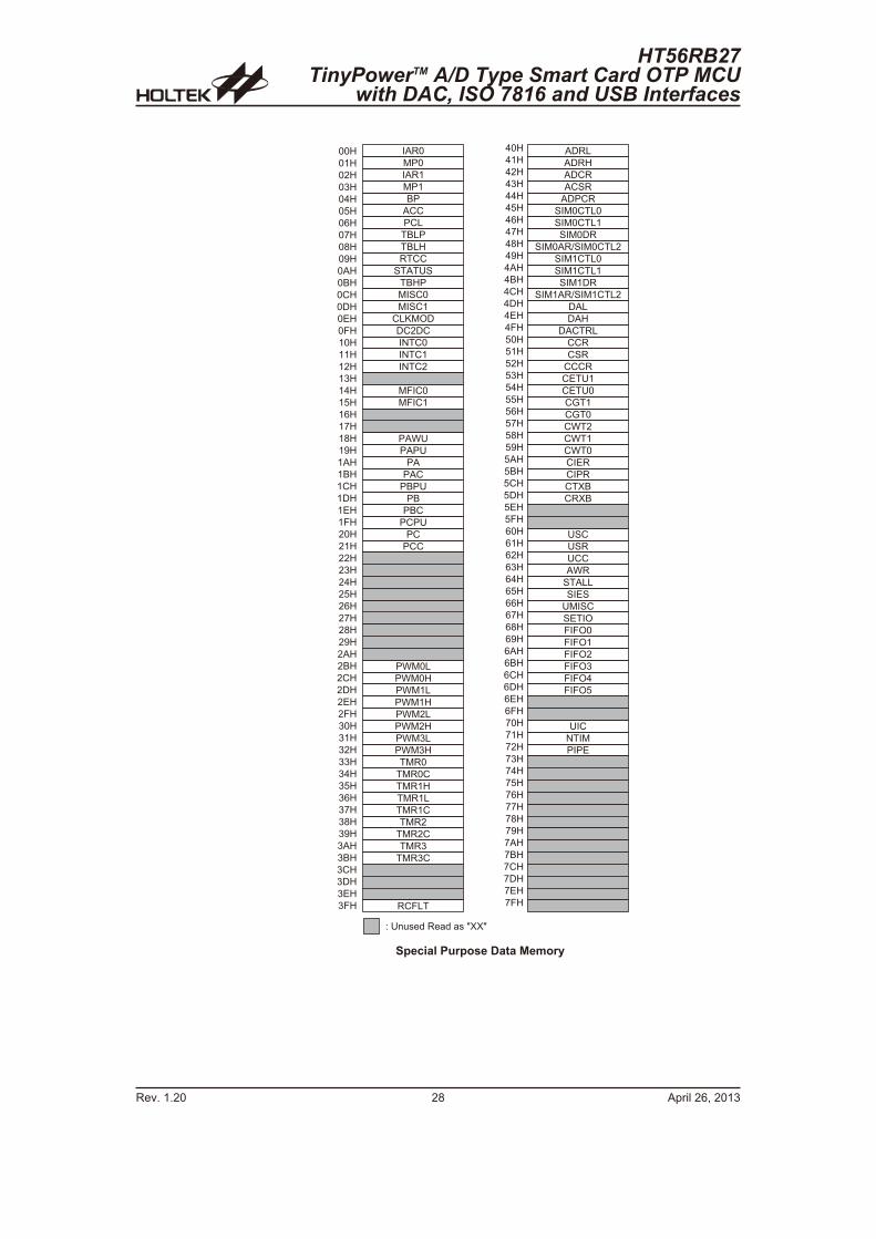
Special Purpose Data Memory
Special Function Registers Description
To ensure successful operation of the microcontroller, certain internal registers are implemented in the
Data Memory area. These registers ensure correct operation of internal functions such as timers,
interrupts, etc., as well as external functions such as I/O data control and A/D converter operation. The
location of these registers within the Data Memory begins at the address �00H�. Any unused Data
Memory locations between these special function registers and the point where the General Purpose
Memory begins is reserved for future expansion purposes, attempting to read data from these locations
will return a unknow value.
Indirect Addressing Registers � IAR0, IAR1
The Indirect Addressing Registers, IAR0 and IAR1, although having their locations in normal RAM
register space, do not actually physically exist as normal registers. The method of indirect addressing
for RAM data manipulation uses these Indirect Addressing Registers and Memory Pointers, in
contrast to direct memory addressing, where the actual memory address is specified. Actions on the
IAR0 and IAR1 registers will result in no actual read or write operation to these registers but rather to
the memory location specified by their corresponding Memory Pointers, MP0 or MP1. Acting as a
pair, IAR0 and MP0 can together access data from Bank 0 while the IAR1 and MP1 register pair can
access data from any bank. As the Indirect Addressing Registers are not physically implemented,
reading the Indirect Addressing Registers indirectly will return a result of �00H� and writing to the
registers indirectly will result in no operation.
Memory Pointers � MP0, MP1
Two Memory Pointers, known as MP0 and MP1 are provided. These Memory Pointers are physically
implemented in the Data Memory and can be manipulated in the same way as normal registers
providing a convenient way with which to address and track data. When any operation to the relevant
Indirect Addressing Registers is carried out, the actual address that the microcontroller is directed to, is
the address specified by the related Memory Pointer. MP0, together with Indirect Addressing Register,
IAR0, are used to access data from Bank 0, while MP1 and IAR1 are used to access data from all
banks.
The following example shows how to clear a section of four RAM locations already defined as
locations adres1 to adres4.
data .section �data�adres1 db ?adres2 db ?adres3 db ?adres4 db ?block db ?code .section at 0 �code�
org 00h
start:mov a,04h ; setup size of blockmov block,amov a,offset adres1 ; Accumulator loaded with first RAM addressmov mp0,a ; setup memory pointer with first RAM address
loop:clr IAR0 ; clear the data at address defined by MP0inc mp0 ; increment memory pointersdz block ; check if last memory location has been clearedjmp loop
continue:
The important point to note here is that in the example shown above, no reference is made to specific RAM addresses.
HT56RB27TinyPowerTM A/D Type Smart Card OTP MCUwith DAC, ISO 7816 and USB Interfaces
Rev. 1.20 29 April 26, 2013
Bank Pointer � BP
The Data Memory is divided into a total of 30 banks. Selecting the required Data Memory area is
achieved using the Bank Pointer. If data in Bank 0 is to be accessed, then the BP register must be
loaded with the value 00H, while if data in Bank 3 is to be accessed, then the BP register must be
loaded with the value 03H, and so on.
The Data Memory is initialised to Bank 0 after a reset, except for the WDT time-out reset in the Power
Down Mode, in which case, the Data Memory bank remains unaffected. It should be noted that the
Special Function Data Memory is not affected by the bank selection, which means that the Special
Function Registers can be accessed from within any bank. Directly addressing the Data Memory will
always result in Bank 0 being accessed irrespective of the value of the Bank Pointer. Accessing data
from banks other than Bank 0 must be implemented using Indirect addressing.
Bit 7 6 5 4 3 2 1 0
Name BP7 BP6 BP5 BP4 BP3 BP2 BP1 BP0
R/W R/W R/W R/W R/W R/W R/W R/W R/W
POR 0 0 0 0 0 0 0 0
Bit 7~5 BP7~BP5: Program Memory Bank Selection bits
000: Program Memory Bank 0
001: Program Memory Bank 1
010: Program Memory Bank 2
011: Program Memory Bank 3
100: Program Memory Bank 4
101: Program Memory Bank 5
110~111: not implemented
| The Program Memory has the capacity of 48K words implemented as 8K words � 6 Banks.
Bit 4~0 BP4~BP0: Data Memory Bank Selection bits
00000: Bank 0 for General Purpose Data Memory
00001~00010: Not exist.
00011~11111: Bank 3 ~ Bank 31 for General Purpose Data Memory
Accumulator � ACC
The Accumulator is central to the operation of any microcontroller and is closely related with
operations carried out by the ALU. The Accumulator is the place where all intermediate results from
the ALU are stored. Without the Accumulator it would be necessary to write the result of each
calculation or logical operation such as addition, subtraction, shift, etc., to the Data Memory resulting
in higher programming and timing overheads. Data transfer operations usually involve the temporary
storage function of the Accumulator; for example, when transferring data between one user defined
register and another, it is necessary to do this by passing the data through the Accumulator as no direct
transfer between two registers is permitted.
Program Counter Low Register � PCL
To provide additional program control functions, the low byte of the Program Counter is made
accessible to programmers by locating it within the Special Purpose area of the Data Memory. By
manipulating this register, direct jumps to other program locations are easily implemented. Loading a
value directly into this PCL register will cause a jump to the specified Program Memory location,
however, as the register is only 8-bit wide, only jumps within the current Program Memory page are
permitted. When such operations are used, note that a dummy cycle will be inserted.
Rev. 1.20 30 April 26, 2013
HT56RB27TinyPowerTM A/D Type Smart Card OTP MCU
with DAC, ISO 7816 and USB Interfaces
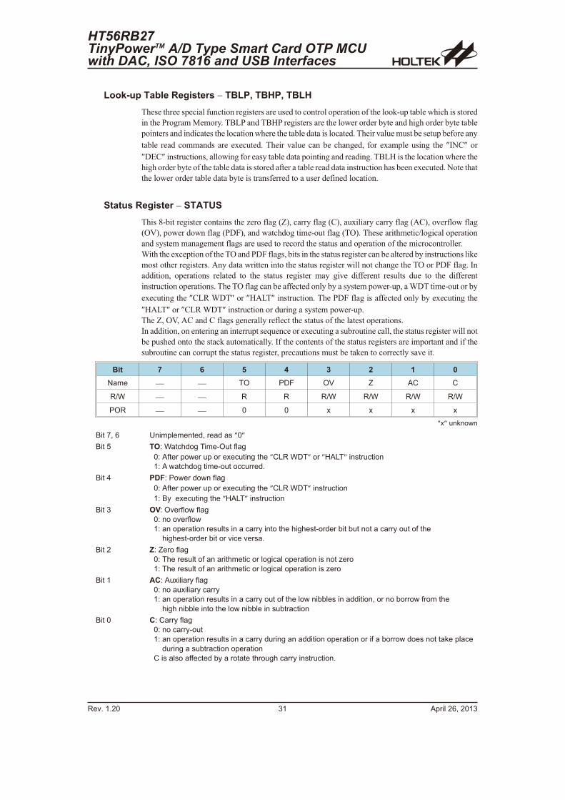
Look-up Table Registers � TBLP, TBHP, TBLH
These three special function registers are used to control operation of the look-up table which is stored
in the Program Memory. TBLP and TBHP registers are the lower order byte and high order byte table
pointers and indicates the location where the table data is located. Their value must be setup before any
table read commands are executed. Their value can be changed, for example using the �INC� or
�DEC� instructions, allowing for easy table data pointing and reading. TBLH is the location where the
high order byte of the table data is stored after a table read data instruction has been executed. Note that
the lower order table data byte is transferred to a user defined location.
Status Register � STATUS
This 8-bit register contains the zero flag (Z), carry flag (C), auxiliary carry flag (AC), overflow flag
(OV), power down flag (PDF), and watchdog time-out flag (TO). These arithmetic/logical operation
and system management flags are used to record the status and operation of the microcontroller.
With the exception of the TO and PDF flags, bits in the status register can be altered by instructions like
most other registers. Any data written into the status register will not change the TO or PDF flag. In
addition, operations related to the status register may give different results due to the different
instruction operations. The TO flag can be affected only by a system power-up, a WDT time-out or by
executing the �CLR WDT� or �HALT� instruction. The PDF flag is affected only by executing the
�HALT� or �CLR WDT� instruction or during a system power-up.
The Z, OV, AC and C flags generally reflect the status of the latest operations.
In addition, on entering an interrupt sequence or executing a subroutine call, the status register will not
be pushed onto the stack automatically. If the contents of the status registers are important and if the
subroutine can corrupt the status register, precautions must be taken to correctly save it.
Bit 7 6 5 4 3 2 1 0
Name � � TO PDF OV Z AC C
R/W � � R R R/W R/W R/W R/W
POR � � 0 0 x x x x
�x� unknown
Bit 7, 6 Unimplemented, read as �0�
Bit 5 TO: Watchdog Time-Out flag
0: After power up or executing the �CLR WDT� or �HALT� instruction
1: A watchdog time-out occurred.
Bit 4 PDF: Power down flag
0: After power up or executing the �CLR WDT� instruction
1: By executing the �HALT� instruction
Bit 3 OV: Overflow flag
0: no overflow
1: an operation results in a carry into the highest-order bit but not a carry out of the
highest-order bit or vice versa.
Bit 2 Z: Zero flag
0: The result of an arithmetic or logical operation is not zero
1: The result of an arithmetic or logical operation is zero
Bit 1 AC: Auxiliary flag
0: no auxiliary carry
1: an operation results in a carry out of the low nibbles in addition, or no borrow from the
high nibble into the low nibble in subtraction
Bit 0 C: Carry flag
0: no carry-out
1: an operation results in a carry during an addition operation or if a borrow does not take place
during a subtraction operation
C is also affected by a rotate through carry instruction.
HT56RB27TinyPowerTM A/D Type Smart Card OTP MCUwith DAC, ISO 7816 and USB Interfaces
Rev. 1.20 31 April 26, 2013
Interrupt Control Registers
These 8-bit registers, known as INTC0, INTC1, INTC2, MFIC0, MFIC1 and MISC0, control the
overall operations of the device interrupt functions. By setting various bits within these registers using
standard bit manipulation instructions, the enable/disable function of each interrupt can be
independently controlled. A master interrupt bit within the INTC0 register, the EMI bit, acts like a
global enable/disable control and is used to set all of the interrupt enable bits on or off. This bit is
cleared when an interrupt subroutine is entered to disable further interrupt and is set by executing the
�RETI� instruction. The MISC0 register is used to select the active edges for the two external interrupt
pins INT0 and INT1.
Timer/Event Counter Registers
The device contains several internal 8-bit and 16-bit Timer/Event Counters. The registers TMR0,
TMR2, TMR3 and the register pair TMR1L/TMR1H are the locations where the timer values are
located. These registers can also be preloaded with fixed data to allow different time intervals to be
setup. The associated control registers, TMR0C, TMR1C, TMR2C and TMR3C contain the setup
information for these timers, which determines in what mode the timer is to be used as well as
containing the timer on/off control function.
Input/Output Ports and Control Registers
Within the area of Special Function Registers, the I/O data registers and their associated control
registers play a prominent role. All I/O ports have a designated register correspondingly labeled as PA,
PB and PC. These labeled I/O registers are mapped to specific addresses within the Data Memory as
shown in the Data Memory table, which are used to transfer the appropriate output or input data on that
port. With each I/O port there is an associated control register labeled PAC, PBC and PCC also mapped
to specific addresses within the Data Memory. The control register specifies which pins of that port are
set as inputs and which are set as outputs. To setup a pin as an input, the corresponding bit of the control
register must be set high while for an output it must be set low. During program initialization, it is
important to first setup the control registers to specify which pins are outputs and which are inputs
before reading data from or writing data to the I/O ports. One flexible feature of these registers is the
ability to directly program single bits using the �SET [m].i� and �CLR [m].i� instructions. The ability
to change I/O pins from output to input and vice versa by manipulating specific bits of the I/O control
registers during normal program operation is a useful feature of these devices.
Pulse Width Modulator Registers
The device contains multiple Pulse Width Modulator outputs each with their own related independent
control register pair, known as PWM0L/PWM0H, PWM1L/PWM1H, PWM2L/PWM2H and
PWM3L/PWM3H. The 12-bit contents of each register pair, which defines the duty cycle value for the
modulation cycle of the Pulse Width Modulator, along with an enable bit are contained in these register
pairs.
A/D Converter Registers � ADRL, ADRH, ADCR, ACSR
The device contains a multiple channel 12-bit A/D converter. The correct operation of the A/D
requires the use of two data registers and two control registers. The two data registers, a high byte data
register known as ADRH, and a low byte data register known as ADRL, are the register locations
where the digital value is placed after the completion of an analog to digital conversion cycle.
Functions such as the A/D enable/disable, A/D channel selection and A/D clock frequency are
determined using the two control registers, ADCR and ACSR.
Rev. 1.20 32 April 26, 2013
HT56RB27TinyPowerTM A/D Type Smart Card OTP MCU
with DAC, ISO 7816 and USB Interfaces
Serial Interface Module Registers
The device contains two Serial Interface Modules named SIM0 and SIM1 and each SIM contains an
SPI and an I2C interface. The SIMxCTL0, SIMxCTL1, SIMxCTL2 and SIMxAR are the control
registers for the Serial Interface function while the SIMxDR is the data register for the Serial Interface
Data where x means 0 and 1.
Port A Wake-up Register � PAWU
All pins on Port A have a wake-up function enable a low going edge on these pins to wake-up the
device when it is in a power down mode. The pins on Port A that are used to have a wake-up function
are selected using this resister.
Pull-High Registers � PAPU, PBPU, PCPU
All I/O pins on Ports PA, PB and PC if setup as inputs, can be connected to an internal pull-high
resistor. The pins which require a pull-high resistor to be connected are selected using these registers.
Clock Control Register � CLKMOD
The device operates using a dual clock system whose mode is controlled using this register. The
register controls functions such as the clock source, the idle mode enable and the division ratio for the
slow clock.
Miscellaneous Register � MISC0, MISC1
These registers name MISC0 and MISC1 are used to control the miscellaneous functions such as the
active edge selection of the external interrupt pins, the clock divided ratio selection of the Smart Card
and the Watchdog Timer enable control bits. There are also four bits used to determine if the output
type is open drain or CMOS output for PA0~PA3.
Input/Output Ports
Holtek microcontroller offer considerable flexibility on their I/O ports. With the input or output
designation of every pin fully under user program control, pull-high selections for all ports and
wake-up selections on certain pins, the user is provided with an I/O structure to meet the needs of a
wide range of application possibilities.
The device provides up to 24 bidirectional input/output lines labeled with port names PA, PB and PC.
These I/O ports are mapped to the RAM Data Memory with specific addresses as shown in the Special
Purpose Data Memory table. All of these I/O ports can be used for input and output operations. For
input operation, these ports are non-latching, which means the inputs must be ready at the T2 rising
edge of instruction �MOV A,[m]�, where m denotes the port address. For output operation, all the data
is latched and remains unchanged until the output latch is rewritten.
Pull-high Resistors
Many product applications require pull-high resistors for their switch inputs usually requiring the use
of an external resistor. To eliminate the need for these external resistors, all I/O pins, when configured
as an input have the capability of being connected to an internal pull-high resistor. These pull-high
resistors are selected using registers PAPU, PBPU and PCPU are implemented using weak PMOS
transistors.
HT56RB27TinyPowerTM A/D Type Smart Card OTP MCUwith DAC, ISO 7816 and USB Interfaces
Rev. 1.20 33 April 26, 2013
PAWU, PAPU, PA, PAC, PBPU, PB, PBC, PCPU, PC and PCC Registers
Register
NamePOR
Bit
7 6 5 4 3 2 1 0
PAWU 00H PAWU7 PAWU6 PAWU5 PAWU4 PAWU3 PAWU2 PAWU1 PAWU0
PAPU 00H PAPU7 PAPU6 PAPU5 PAPU4 PAPU3 PAPU2 PAPU1 PAPU0
PA FFH PA7 PA6 PA5 PA4 PA3 PA2 PA1 PA0
PAC FFH PAC7 PAC6 PAC5 PAC4 PAC3 PAC2 PAC1 PAC0
PBPU 00H PBPU7 PBPU6 PBPU5 PBPU4 PBPU3 PBPU2 PBPU1 PBPU0
PB FFH PB7 PB6 PB5 PB4 PB3 PB2 PB1 PB0
PBC FFH PBC7 PBC6 PBC5 PBC4 PBC3 PBC2 PBC1 PBC0
PCPU 00H PCPU7 PCPU6 PCPU5 PCPU4 PCPU3 PCPU2 PCPU1 PCPU0
PC FFH PC7 PC6 PC5 PC4 PC3 PC2 PC1 PC0
PCC FFH PCC7 PCC6 PCC5 PCC4 PCC3 PCC2 PCC1 PCC0
PAWUn: PA wake-up function enable
0: disable
1: enable
PAPUn/PBPUn/PCPUn: Pull-high function enable
0: disable
1: enable
PAn/PBn/PCn: I/O port data bit
PACn/PBCn/PCCn: I/O port type selection bit
0: output
1: input
Port A Wake-up
The HALT instruction forces the microcontroller into a Power Down condition which preserves
power, a feature that is important for battery and otuher low-power applications. Various methods exist
to wake-up the microcontroller, one of which is to change the logic condition on one of the Port A pins
from high to low. After a HALT instruction forces the microcontroller into entering a Power Down
condition, the processor will remain in a low-power state until the logic condition of the selected
wake-up pin on Port A changes from high to low. This function is especially suitable for applications
that can be woken up via external switches. Each pin on Port Acan be selected individually to have this
wake-up feature using the PAWU register.
Rev. 1.20 34 April 26, 2013
HT56RB27TinyPowerTM A/D Type Smart Card OTP MCU
with DAC, ISO 7816 and USB Interfaces
Port A Open Drain Function
All I/O pins in the device have CMOS structures, however Port A pins PA0~PA3 can also be setup as
open drain structures. This is implemented using the ODE0~ ODE3 bits in the MISC1 register.
MISC1 Register
Bit 7 6 5 4 3 2 1 0
Name ODE3 ODE2 ODE1 ODE0 WDTEN3 WDTEN2 WDTEN1 WDTEN0
R/W R/W R/W R/W R/W R/W R/W R/W R/W
POR 0 0 0 0 1 0 1 0
Bit 7 ODE3: PA3 Open Drain control
0: disable
1: enable
Bit 6 ODE2: PA2 Open Drain control
0: disable
1: enable
Bit 5 ODE1: PA1 Open Drain control
0: disable
1: enable
Bit 4 ODE0: PA0 Open Drain control
0: disable
1: enable
Bit 3~0 WDTEN3, WDTEN2, WDTEN1, WDTEN0: WDT function enable
Described in Watchdog Timer section.
I/O Port Control Registers
Each I/O port has its own control register known as PAC, PBC, etc., to control the input/output
configuration. With this control register, each CMOS output or input with or without pull-high resistor
structures can be reconfigured dynamically under software control. Each pin of the I/O ports is directly
mapped to a bit in its associated port control register. For the I/O pin to function as an input, the
corresponding bit of the control register must be written as a �1�. This will then allow the logic state of
the input pin to be directly read by instructions. When the corresponding bit of the control register is
written as a �0�, the I/O pin will be setup as a CMOS output. If the pin is currently setup as an output,
instructions can still be used to read the output register. However, it should be noted that the program
will in fact only read the status of the output data latch and not the actual logic status of the output pin.
HT56RB27TinyPowerTM A/D Type Smart Card OTP MCUwith DAC, ISO 7816 and USB Interfaces
Rev. 1.20 35 April 26, 2013
Pin-shared Functions
The flexibility of the microcontroller range is greatly enhanced by the use of pins that have more than
one function. Limited numbers of pins can force serious design constraints on designers but by
supplying pins with multi-functions, many of these difficulties can be overcome. For some pins, the
chosen function of the multi-function I/O pins is set by configuration options while for others the
function is set by application program control.
� External Interrupt Inputs
The external interrupt pins INT0 and INT1 are pin-shared with the I/O pins PA0 and PA1. For
applications not requiring an external interrupt input, the pin-shared external interrupt pin can be
used as a normal I/O pin, however to do this, the external interrupt enable bits in the INTC0 register
must be disabled.
� External Timer Clock Input
The external timer pins TMR0, TMR1, TMR2 and TMR3 are pin-shared with I/O pins. To configure
them to operate as timer inputs, the corresponding control bits in the timer control register must be
correctly set and the pin must also be setup as an input. Note that the original I/O function will
remain even if the pin is setup to be used as an external timer input.
� PFD Output
The device contains a PFD function whose single output is pin-shared with I/O pin PA3. The output
function of this pin is chosen via a configuration option and remains fixed after the device is
programmed. Note that the corresponding bit of the port control register, PAC.3, must setup the pin
as an output to enable the PFD output. If the PAC port control register has setup the pin as an input,
then the pin will function as a normal logic input with the usual pull-high selection, even if the PFD
configuration option has been selected.
� PWM Outputs
The device contains several PWM outputs name PWM0~PWM3 shared with pins PC4~PC6 and
PA5. The PWM output functions are chosen via registers. Note that the corresponding bit of the port
control register bit must setup the pin as an output to enable the PWM output. If the port control
register bit has setup the pin as an input, then the pin will function as a normal logic input with the
usual pull-high selection, even if the PWM registers have enabled the PWM function.
� A/D Inputs
The device contains a multi-channel A/D converter inputs. All of these analog inputs are pin-shared
with I/O pins on Port A. If these pins are to be used as A/D inputs and not as normal I/O pins then the
corresponding bits in the A/D Converter Control Register, ADCR, must be properly set. There are no
configuration options associated with the A/D function. If used as I/O pins, then full pull-high
resistor register remain, however if used as A/D inputs then any pull-high resistor selections
associated with these pins will be automatically disconnected.
I/O Pin Structures
The accompanying diagrams illustrate the internal structures of some I/O pin types. As the exact
logical construction of the I/O pin will differ from these drawings, they are supplied as a guide only to
assist with the functional understanding of the I/O pins. The wide range of pin-shared structures does
not permit all types to be shown.
Rev. 1.20 36 April 26, 2013
HT56RB27TinyPowerTM A/D Type Smart Card OTP MCU
with DAC, ISO 7816 and USB Interfaces
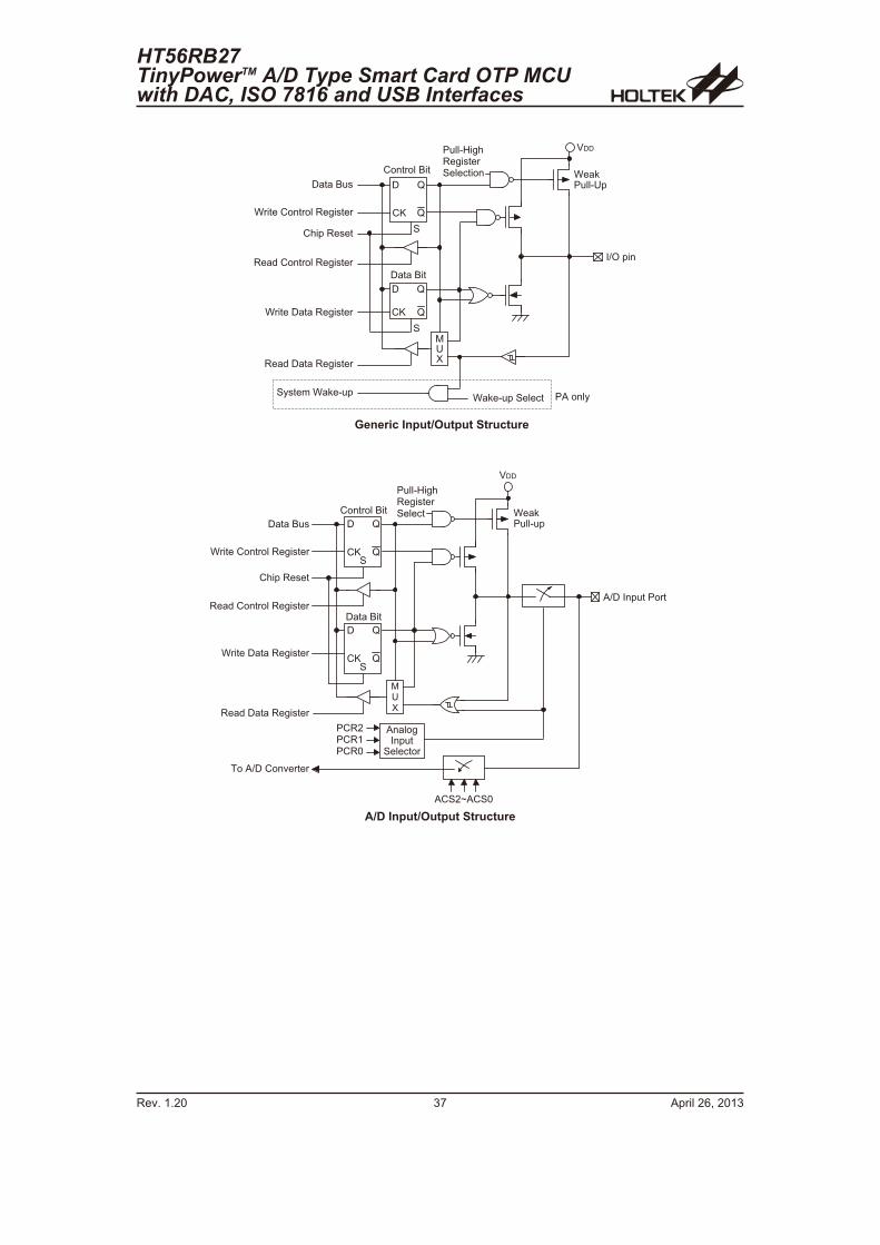
HT56RB27TinyPowerTM A/D Type Smart Card OTP MCUwith DAC, ISO 7816 and USB Interfaces
Rev. 1.20 37 April 26, 2013
� � �
/>D
C � " � � � ( � # � � � �# $ � � � � � C � " � � � (
� � ; � � � � � � � % � � � � !
� F
� B
#
� F
� B
#
� � � ! � � 8 � �
� � � � � 8 � �
C ! � � � � � � � ! � � � % � � � � !
� � � ( � � � � �
� � ; � � � � ! � � � % � � � � !
C ! � � � � � � � � � � % � � � � !
� � � � � 8 � �
� = � ( � �
F
F
� , � � � $
C � � "� � � � � > (
� � � � � 2 � % � � % � � � � !# � � � � � �
Generic Input/Output Structure
� � �
/>D
� � ; � � � � � � � % � � � � !
� � � ! � � 8 � �
� � � � � 8 � �
C ! � � � � � � � ! � � � % � � � � !
� � � ( � � � � �
� � ; � � � � ! � � � % � � � � !
C ! � � � � � � � � � � % � � � � !
� � � � � 8 � �
, = � � � � ( � � � � ! �
, � # � G , � # 7
� � , = � � � � 9 � ! � � !
� � �� � �� � 7
C � � "� � � � � � (
, � � � %� � ( � �
# � � � � !
� F
� B#
F
� F
� B#
F
� � � � � 2 � % � � % � � � � !# � � � �
A/D Input/Output Structure
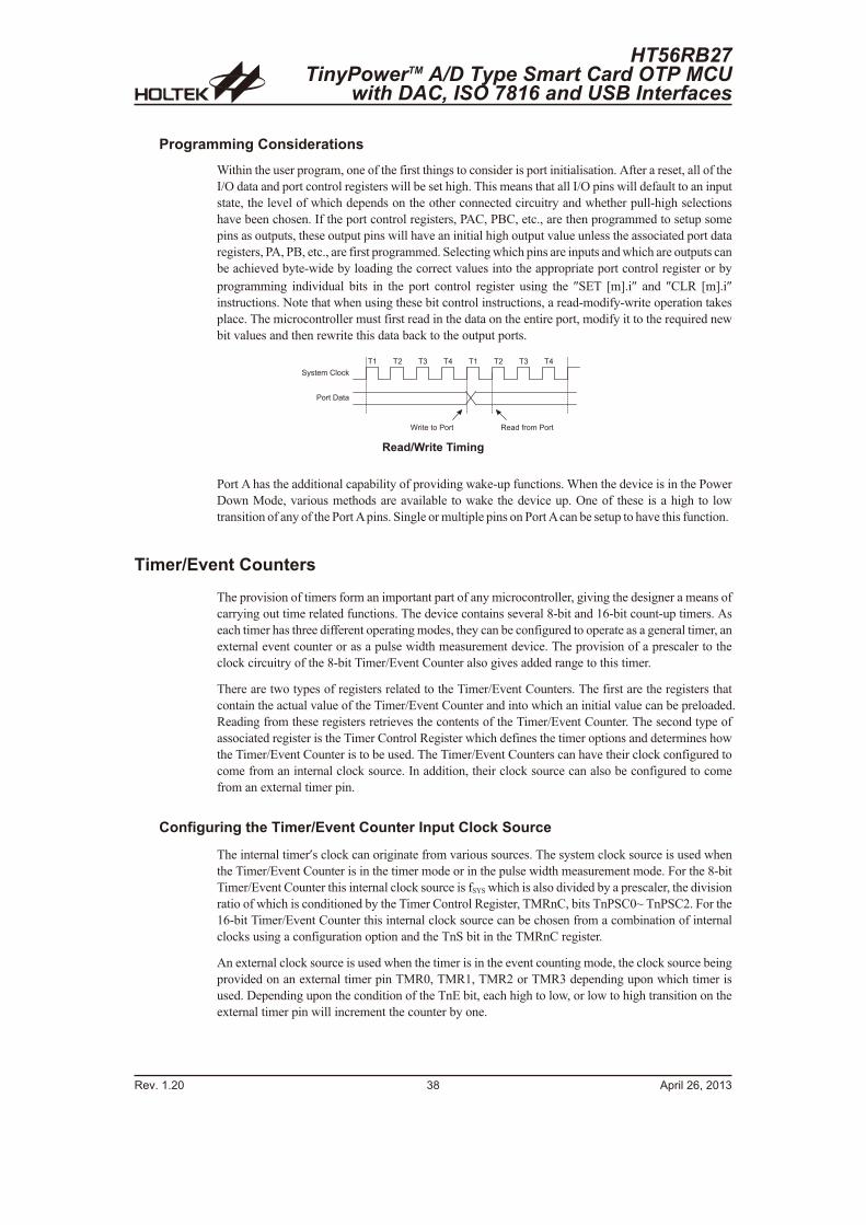
Programming Considerations
Within the user program, one of the first things to consider is port initialisation. After a reset, all of the
I/O data and port control registers will be set high. This means that all I/O pins will default to an input
state, the level of which depends on the other connected circuitry and whether pull-high selections
have been chosen. If the port control registers, PAC, PBC, etc., are then programmed to setup some
pins as outputs, these output pins will have an initial high output value unless the associated port data
registers, PA, PB, etc., are first programmed. Selecting which pins are inputs and which are outputs can
be achieved byte-wide by loading the correct values into the appropriate port control register or by
programming individual bits in the port control register using the �SET [m].i� and �CLR [m].i�
instructions. Note that when using these bit control instructions, a read-modify-write operation takes
place. The microcontroller must first read in the data on the entire port, modify it to the required new
bit values and then rewrite this data back to the output ports.
Port A has the additional capability of providing wake-up functions. When the device is in the Power
Down Mode, various methods are available to wake the device up. One of these is a high to low
transition of any of the Port Apins. Single or multiple pins on Port Acan be setup to have this function.
Timer/Event Counters
The provision of timers form an important part of any microcontroller, giving the designer a means of
carrying out time related functions. The device contains several 8-bit and 16-bit count-up timers. As
each timer has three different operating modes, they can be configured to operate as a general timer, an
external event counter or as a pulse width measurement device. The provision of a prescaler to the
clock circuitry of the 8-bit Timer/Event Counter also gives added range to this timer.
There are two types of registers related to the Timer/Event Counters. The first are the registers that
contain the actual value of the Timer/Event Counter and into which an initial value can be preloaded.
Reading from these registers retrieves the contents of the Timer/Event Counter. The second type of
associated register is the Timer Control Register which defines the timer options and determines how
the Timer/Event Counter is to be used. The Timer/Event Counters can have their clock configured to
come from an internal clock source. In addition, their clock source can also be configured to come
from an external timer pin.
Configuring the Timer/Event Counter Input Clock Source
The internal timer�s clock can originate from various sources. The system clock source is used when
the Timer/Event Counter is in the timer mode or in the pulse width measurement mode. For the 8-bit
Timer/Event Counter this internal clock source is fSYS which is also divided by a prescaler, the division
ratio of which is conditioned by the Timer Control Register, TMRnC, bits TnPSC0~ TnPSC2. For the
16-bit Timer/Event Counter this internal clock source can be chosen from a combination of internal
clocks using a configuration option and the TnS bit in the TMRnC register.
An external clock source is used when the timer is in the event counting mode, the clock source being
provided on an external timer pin TMR0, TMR1, TMR2 or TMR3 depending upon which timer is
used. Depending upon the condition of the TnE bit, each high to low, or low to high transition on the
external timer pin will increment the counter by one.
Rev. 1.20 38 April 26, 2013
HT56RB27TinyPowerTM A/D Type Smart Card OTP MCU
with DAC, ISO 7816 and USB Interfaces
� � � � � & � ' � � � � � & � '
C ! � � � � � � � ! � � � ; � : ! � � � ! �
# $ � � � � � � � "
� ! � � � � � �
Read/Write Timing
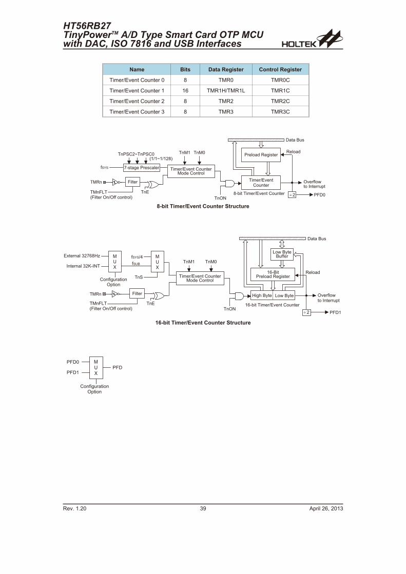
Name Bits Data Register Control Register
Timer/Event Counter 0 8 TMR0 TMR0C
Timer/Event Counter 1 16 TMR1H/TMR1L TMR1C
Timer/Event Counter 2 8 TMR2 TMR2C
Timer/Event Counter 3 8 TMR3 TMR3C
HT56RB27TinyPowerTM A/D Type Smart Card OTP MCUwith DAC, ISO 7816 and USB Interfaces
Rev. 1.20 39 April 26, 2013
� / �
� � � � ! = � 9 � � � � � � � � � !/ ; � � � � � ! �
� � 4
� ! � � � ; � � % � � � � !
� � � � ! = � 9 � � �� � � � � !
� � � � � 8 � �
� � � ;
9 � ! : � ?� � � � � � ! ! � ( �
� � � �
5 � � � � % � � � ! � � � � � !
� � � # � � G � � � # � 7� � = � G � = � � 6 �
6 � < � � � � � � � ! = � 9 � � � � � � � � � !
� � / � � � / 7
� � : # - #
� � � 7�� � �
� � � � � !
� / � � + �� � � � � � ! � � = : : � � � ! � �
8-bit Timer/Event Counter Structure
� / �
� � �
� � � � ! = � 9 � � � � � � � � � !/ ; � � � � � ! �
� * � 8 � �� ! � � � ; � � % � � � � !
� � � � � 8 � �
� � � ;
9 � ! : � ?� � � � � � ! ! � ( �
+ ? � 8 $ � �8 � : : � !
� � / � � � / 7
� � 4
2 � % � � 8 $ � � + ? � 8 $ � �
� * � < � � � � � � � ! = � 9 � � � � � � � � � !
� � � �� � � ��
� � #
/>D �
� � : # - # = '/>D �
� � : # > 8
� � � � ! � � � � & � 5 * 6 2 H
� � � � ! � � � � & � B � � 4 �
� � : � % � ! � � � � ( � � �
� � � � � !
� / � � + �� � � � � � ! � � = : : � � � ! � �
16-bit Timer/Event Counter Structure
/>D �
� � � 7
� � � �
� � : � % � ! � � � � ( � � �
� � �
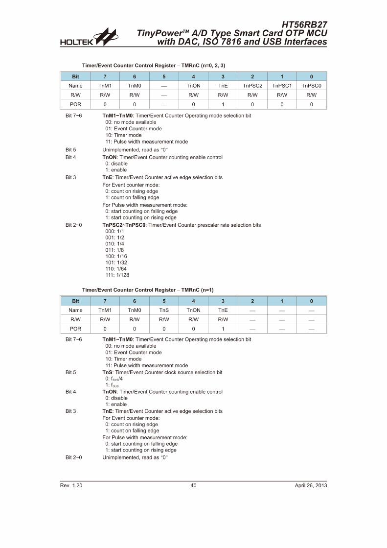
Timer/Event Counter Control Register � TMRnC (n=0, 2, 3)
Bit 7 6 5 4 3 2 1 0
Name TnM1 TnM0 � TnON TnE TnPSC2 TnPSC1 TnPSC0
R/W R/W R/W � R/W R/W R/W R/W R/W
POR 0 0 � 0 1 0 0 0
Bit 7~6 TnM1~TnM0: Timer/Event Counter Operating mode selection bit
00: no mode available
01: Event Counter mode
10: Timer mode
11: Pulse width measurement mode
Bit 5 Unimplemented, read as �0�
Bit 4 TnON: Timer/Event Counter counting enable control0: disable1: enable
Bit 3 TnE: Timer/Event Counter active edge selection bits
For Event counter mode:0: count on rising edge1: count on falling edge
For Pulse width measurement mode:0: start counting on falling edge1: start counting on rising edge
Bit 2~0 TnPSC2~TnPSC0: Timer/Event Counter prescaler rate selection bits000: 1/1001: 1/2010: 1/4011: 1/8100: 1/16101: 1/32110: 1/64111: 1/128
Timer/Event Counter Control Register � TMRnC (n=1)
Bit 7 6 5 4 3 2 1 0
Name TnM1 TnM0 TnS TnON TnE � � �
R/W R/W R/W R/W R/W R/W � � �
POR 0 0 0 0 1 � � �
Bit 7~6 TnM1~TnM0: Timer/Event Counter Operating mode selection bit
00: no mode available
01: Event Counter mode
10: Timer mode
11: Pulse width measurement mode
Bit 5 TnS: Timer/Event Counter clock source selection bit0: fSYS/41: fSUB
Bit 4 TnON: Timer/Event Counter counting enable control0: disable1: enable
Bit 3 TnE: Timer/Event Counter active edge selection bits
For Event counter mode:0: count on rising edge1: count on falling edge
For Pulse width measurement mode:0: start counting on falling edge1: start counting on rising edge
Bit 2~0 Unimplemented, read as �0�
Rev. 1.20 40 April 26, 2013
HT56RB27TinyPowerTM A/D Type Smart Card OTP MCU
with DAC, ISO 7816 and USB Interfaces
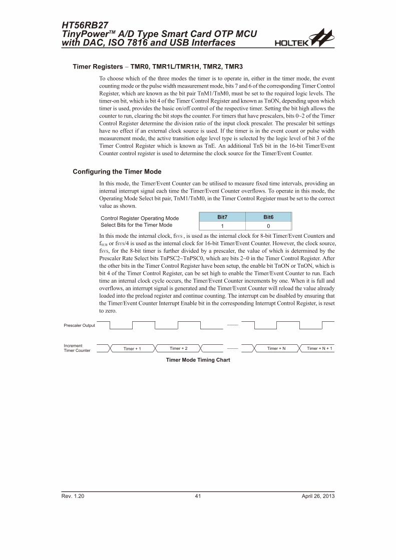
Timer Registers � TMR0, TMR1L/TMR1H, TMR2, TMR3
To choose which of the three modes the timer is to operate in, either in the timer mode, the event
counting mode or the pulse width measurement mode, bits 7 and 6 of the corresponding Timer Control
Register, which are known as the bit pair TnM1/TnM0, must be set to the required logic levels. The
timer-on bit, which is bit 4 of the Timer Control Register and known as TnON, depending upon which
timer is used, provides the basic on/off control of the respective timer. Setting the bit high allows the
counter to run, clearing the bit stops the counter. For timers that have prescalers, bits 0~2 of the Timer
Control Register determine the division ratio of the input clock prescaler. The prescaler bit settings
have no effect if an external clock source is used. If the timer is in the event count or pulse width
measurement mode, the active transition edge level type is selected by the logic level of bit 3 of the
Timer Control Register which is known as TnE. An additional TnS bit in the 16-bit Timer/Event
Counter control register is used to determine the clock source for the Timer/Event Counter.
Configuring the Timer Mode
In this mode, the Timer/Event Counter can be utilised to measure fixed time intervals, providing an
internal interrupt signal each time the Timer/Event Counter overflows. To operate in this mode, the
Operating Mode Select bit pair, TnM1/TnM0, in the Timer Control Register must be set to the correct
value as shown.
Control Register Operating Mode
Select Bits for the Timer Mode
Bit7 Bit6
1 0
In this mode the internal clock, fSYS , is used as the internal clock for 8-bit Timer/Event Counters and
fSUB or fSYS/4 is used as the internal clock for 16-bit Timer/Event Counter. However, the clock source,
fSYS, for the 8-bit timer is further divided by a prescaler, the value of which is determined by the
Prescaler Rate Select bits TnPSC2~TnPSC0, which are bits 2~0 in the Timer Control Register. After
the other bits in the Timer Control Register have been setup, the enable bit TnON or TnON, which is
bit 4 of the Timer Control Register, can be set high to enable the Timer/Event Counter to run. Each
time an internal clock cycle occurs, the Timer/Event Counter increments by one. When it is full and
overflows, an interrupt signal is generated and the Timer/Event Counter will reload the value already
loaded into the preload register and continue counting. The interrupt can be disabled by ensuring that
the Timer/Event Counter Interrupt Enable bit in the corresponding Interrupt Control Register, is reset
to zero.
HT56RB27TinyPowerTM A/D Type Smart Card OTP MCUwith DAC, ISO 7816 and USB Interfaces
Rev. 1.20 41 April 26, 2013
� � ! � � � � �� � � � ! � � � � � � !
� ! � � � � � ! � � � ( � �
� � � � ! � � � � � � � � ! � � � � � � � � ! � � � 4 � � � � ! � � � 4 � � � �
Timer Mode Timing Chart
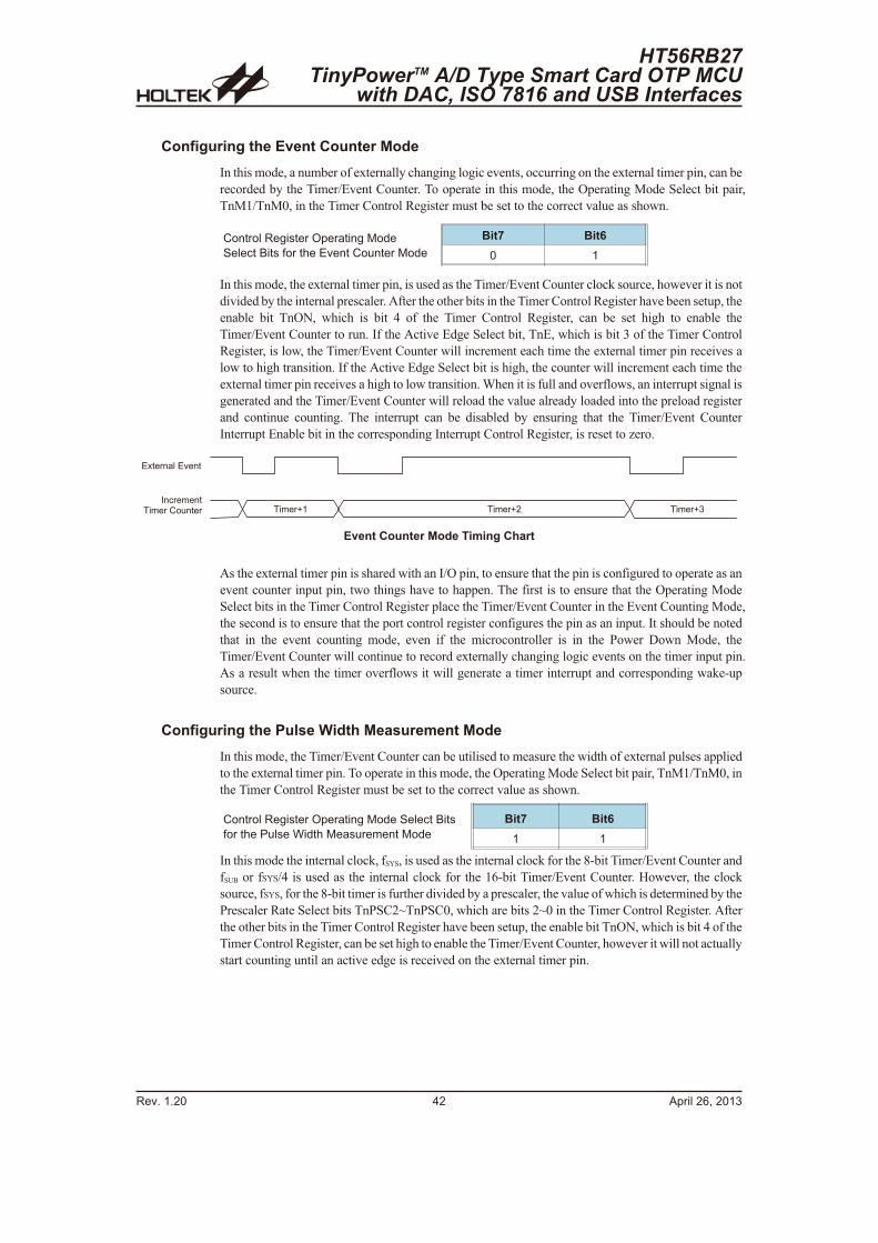
Configuring the Event Counter Mode
In this mode, a number of externally changing logic events, occurring on the external timer pin, can be
recorded by the Timer/Event Counter. To operate in this mode, the Operating Mode Select bit pair,
TnM1/TnM0, in the Timer Control Register must be set to the correct value as shown.
Control Register Operating Mode
Select Bits for the Event Counter Mode
Bit7 Bit6
0 1
In this mode, the external timer pin, is used as the Timer/Event Counter clock source, however it is not
divided by the internal prescaler. After the other bits in the Timer Control Register have been setup, the
enable bit TnON, which is bit 4 of the Timer Control Register, can be set high to enable the
Timer/Event Counter to run. If the Active Edge Select bit, TnE, which is bit 3 of the Timer Control
Register, is low, the Timer/Event Counter will increment each time the external timer pin receives a
low to high transition. If the Active Edge Select bit is high, the counter will increment each time the
external timer pin receives a high to low transition. When it is full and overflows, an interrupt signal is
generated and the Timer/Event Counter will reload the value already loaded into the preload register
and continue counting. The interrupt can be disabled by ensuring that the Timer/Event Counter
Interrupt Enable bit in the corresponding Interrupt Control Register, is reset to zero.
As the external timer pin is shared with an I/O pin, to ensure that the pin is configured to operate as an
event counter input pin, two things have to happen. The first is to ensure that the Operating Mode
Select bits in the Timer Control Register place the Timer/Event Counter in the Event Counting Mode,
the second is to ensure that the port control register configures the pin as an input. It should be noted
that in the event counting mode, even if the microcontroller is in the Power Down Mode, the
Timer/Event Counter will continue to record externally changing logic events on the timer input pin.
As a result when the timer overflows it will generate a timer interrupt and corresponding wake-up
source.
Configuring the Pulse Width Measurement Mode
In this mode, the Timer/Event Counter can be utilised to measure the width of external pulses applied
to the external timer pin. To operate in this mode, the Operating Mode Select bit pair, TnM1/TnM0, in
the Timer Control Register must be set to the correct value as shown.
Control Register Operating Mode Select Bits
for the Pulse Width Measurement Mode
Bit7 Bit6
1 1
In this mode the internal clock, fSYS, is used as the internal clock for the 8-bit Timer/Event Counter and
fSUB or fSYS/4 is used as the internal clock for the 16-bit Timer/Event Counter. However, the clock
source, fSYS, for the 8-bit timer is further divided by a prescaler, the value of which is determined by the
Prescaler Rate Select bits TnPSC2~TnPSC0, which are bits 2~0 in the Timer Control Register. After
the other bits in the Timer Control Register have been setup, the enable bit TnON, which is bit 4 of the
Timer Control Register, can be set high to enable the Timer/Event Counter, however it will not actually
start counting until an active edge is received on the external timer pin.
Rev. 1.20 42 April 26, 2013
HT56RB27TinyPowerTM A/D Type Smart Card OTP MCU
with DAC, ISO 7816 and USB Interfaces
� � � � ! � �
� � � � ! � � � � � 9 � � �
� � ! � � � � �� � � � ! � � � � � � ! � � � � ! � &� � � � ! � �
Event Counter Mode Timing Chart
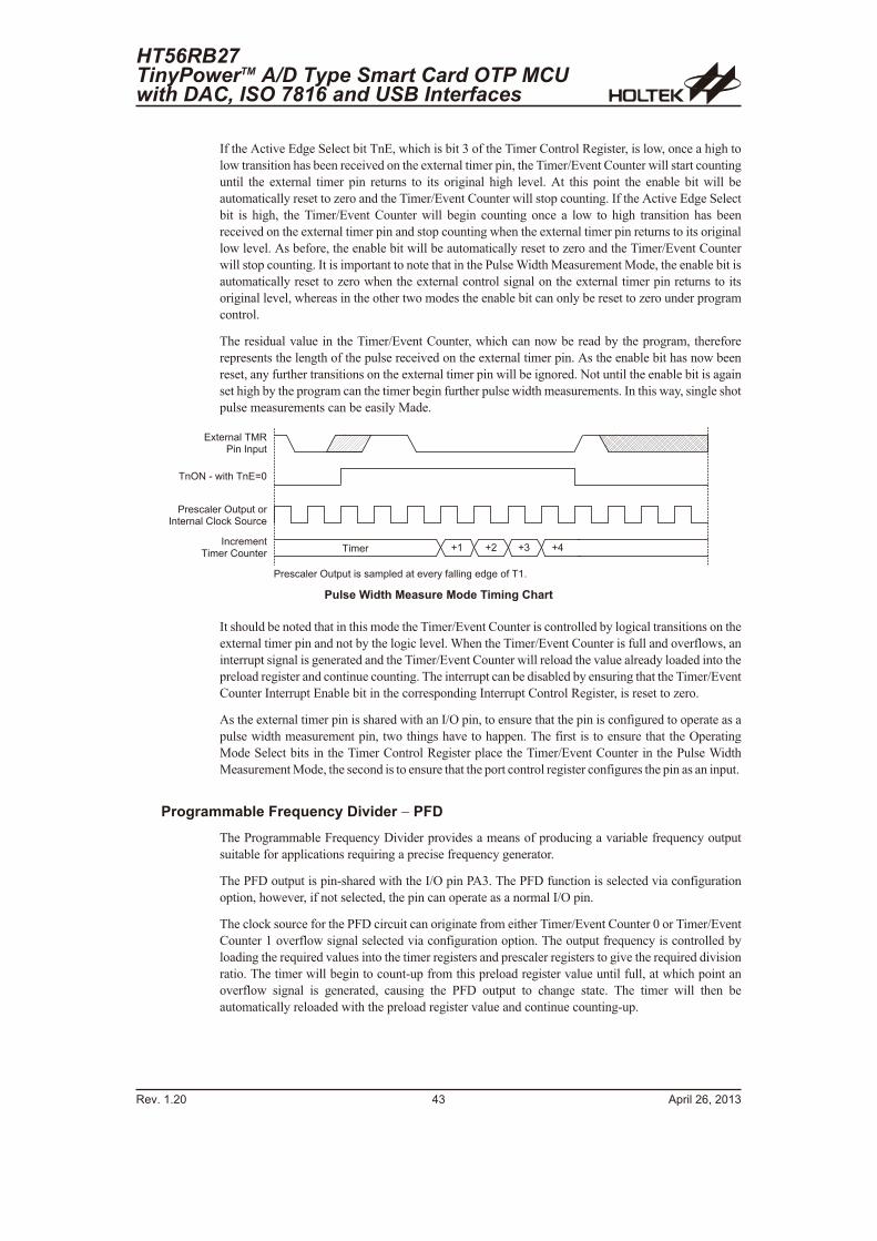
If the Active Edge Select bit TnE, which is bit 3 of the Timer Control Register, is low, once a high to
low transition has been received on the external timer pin, the Timer/Event Counter will start counting
until the external timer pin returns to its original high level. At this point the enable bit will be
automatically reset to zero and the Timer/Event Counter will stop counting. If the Active Edge Select
bit is high, the Timer/Event Counter will begin counting once a low to high transition has been
received on the external timer pin and stop counting when the external timer pin returns to its original
low level. As before, the enable bit will be automatically reset to zero and the Timer/Event Counter
will stop counting. It is important to note that in the Pulse Width Measurement Mode, the enable bit is
automatically reset to zero when the external control signal on the external timer pin returns to its
original level, whereas in the other two modes the enable bit can only be reset to zero under program
control.
The residual value in the Timer/Event Counter, which can now be read by the program, therefore
represents the length of the pulse received on the external timer pin. As the enable bit has now been
reset, any further transitions on the external timer pin will be ignored. Not until the enable bit is again
set high by the program can the timer begin further pulse width measurements. In this way, single shot
pulse measurements can be easily Made.
It should be noted that in this mode the Timer/Event Counter is controlled by logical transitions on the
external timer pin and not by the logic level. When the Timer/Event Counter is full and overflows, an
interrupt signal is generated and the Timer/Event Counter will reload the value already loaded into the
preload register and continue counting. The interrupt can be disabled by ensuring that the Timer/Event
Counter Interrupt Enable bit in the corresponding Interrupt Control Register, is reset to zero.
As the external timer pin is shared with an I/O pin, to ensure that the pin is configured to operate as a
pulse width measurement pin, two things have to happen. The first is to ensure that the Operating
Mode Select bits in the Timer Control Register place the Timer/Event Counter in the Pulse Width
Measurement Mode, the second is to ensure that the port control register configures the pin as an input.
Programmable Frequency Divider � PFD
The Programmable Frequency Divider provides a means of producing a variable frequency output
suitable for applications requiring a precise frequency generator.
The PFD output is pin-shared with the I/O pin PA3. The PFD function is selected via configuration
option, however, if not selected, the pin can operate as a normal I/O pin.
The clock source for the PFD circuit can originate from either Timer/Event Counter 0 or Timer/Event
Counter 1 overflow signal selected via configuration option. The output frequency is controlled by
loading the required values into the timer registers and prescaler registers to give the required division
ratio. The timer will begin to count-up from this preload register value until full, at which point an
overflow signal is generated, causing the PFD output to change state. The timer will then be
automatically reloaded with the preload register value and continue counting-up.
HT56RB27TinyPowerTM A/D Type Smart Card OTP MCUwith DAC, ISO 7816 and USB Interfaces
Rev. 1.20 43 April 26, 2013
� � � � � & � '� � � � !
� � � � ! � � � � � / � � � � � � ( � �
� � 4 � � � ? � � � � � � � I 7
� ! � � � � � ! � � � ( � � � !� � � � ! � � � � � � " � # � ! �
� � ! � � � � �� � � � ! � � � � � � !
� ! � � � � � ! � � � ( � � � � � � � � � ( � � ; � � � � � 9 � ! $ � : � � � � � % � � ; % � � : � � � �
Pulse Width Measure Mode Timing Chart
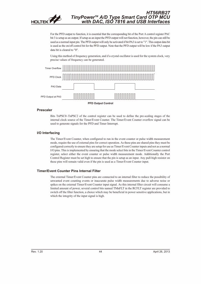
For the PFD output to function, it is essential that the corresponding bit of the Port A control register PAC
bit 3 is setup as an output. If setup as an input the PFD output will not function, however, the pin can still be
used as a normal input pin. The PFD output will only be activated if bit PA3 is set to �1�. This output data bit
is used as the on/off control bit for the PFD output. Note that the PFD output will be low if the PA3 output
data bit is cleared to �0�.
Using this method of frequency generation, and if a crystal oscillator is used for the system clock, very
precise values of frequency can be generated.
Prescaler
Bits TnPSC0~TnPSC2 of the control register can be used to define the pre-scaling stages of the
internal clock source of the Timer/Event Counter. The Timer/Event Counter overflow signal can be
used to generate signals for the PFD and Timer Interrupt.
I/O Interfacing
The Timer/Event Counter, when configured to run in the event counter or pulse width measurement
mode, require the use of external pins for correct operation. As these pins are shared pins they must be
configured correctly to ensure they are setup for use as Timer/Event Counter inputs and not as a normal
I/O pins. This is implemented by ensuring that the mode select bits in the Timer/Event Counter control
register, select either the event counter or pulse width measurement mode. Additionally the Port
Control Register must be set high to ensure that the pin is setup as an input. Any pull-high resistor on
these pins will remain valid even if the pin is used as a Timer/Event Counter input.
Timer/Event Counter Pins Internal Filter
The external Timer/Event Counter pins are connected to an internal filter to reduce the possibility of
unwanted event counting events or inaccurate pulse width measurements due to adverse noise or
spikes on the external Timer/Event Counter input signal. As this internal filter circuit will consume a
limited amount of power, several control bits named TMnFLT in the RCFLT register are provided to
switch off the filter function, a choice which may be beneficial in power sensitive applications, but in
which the integrity of the input signal is high.
Rev. 1.20 44 April 26, 2013
HT56RB27TinyPowerTM A/D Type Smart Card OTP MCU
with DAC, ISO 7816 and USB Interfaces
� � � � ! � 9 � ! : � ?
� � � � � � "
� , & � � � � �
� � � � � � ( � � � � � � � , &
PFD Output Control
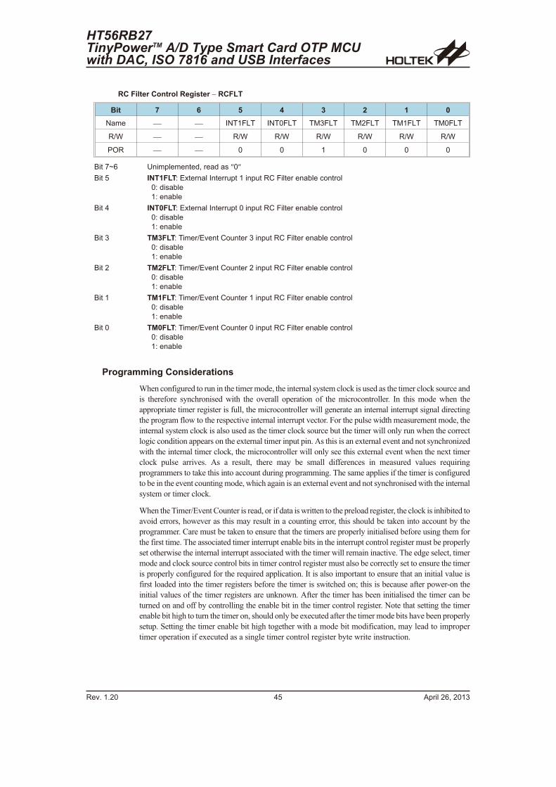
RC Filter Control Register � RCFLT
Bit 7 6 5 4 3 2 1 0
Name � � INT1FLT INT0FLT TM3FLT TM2FLT TM1FLT TM0FLT
R/W � � R/W R/W R/W R/W R/W R/W
POR � � 0 0 1 0 0 0
Bit 7~6 Unimplemented, read as �0�
Bit 5 INT1FLT: External Interrupt 1 input RC Filter enable control
0: disable
1: enable
Bit 4 INT0FLT: External Interrupt 0 input RC Filter enable control
0: disable
1: enable
Bit 3 TM3FLT: Timer/Event Counter 3 input RC Filter enable control
0: disable
1: enable
Bit 2 TM2FLT: Timer/Event Counter 2 input RC Filter enable control
0: disable
1: enable
Bit 1 TM1FLT: Timer/Event Counter 1 input RC Filter enable control
0: disable
1: enable
Bit 0 TM0FLT: Timer/Event Counter 0 input RC Filter enable control
0: disable
1: enable
Programming Considerations
When configured to run in the timer mode, the internal system clock is used as the timer clock source and
is therefore synchronised with the overall operation of the microcontroller. In this mode when the
appropriate timer register is full, the microcontroller will generate an internal interrupt signal directing
the program flow to the respective internal interrupt vector. For the pulse width measurement mode, the
internal system clock is also used as the timer clock source but the timer will only run when the correct
logic condition appears on the external timer input pin. As this is an external event and not synchronized
with the internal timer clock, the microcontroller will only see this external event when the next timer
clock pulse arrives. As a result, there may be small differences in measured values requiring
programmers to take this into account during programming. The same applies if the timer is configured
to be in the event counting mode, which again is an external event and not synchronised with the internal
system or timer clock.
When the Timer/Event Counter is read, or if data is written to the preload register, the clock is inhibited to
avoid errors, however as this may result in a counting error, this should be taken into account by the
programmer. Care must be taken to ensure that the timers are properly initialised before using them for
the first time. The associated timer interrupt enable bits in the interrupt control register must be properly
set otherwise the internal interrupt associated with the timer will remain inactive. The edge select, timer
mode and clock source control bits in timer control register must also be correctly set to ensure the timer
is properly configured for the required application. It is also important to ensure that an initial value is
first loaded into the timer registers before the timer is switched on; this is because after power-on the
initial values of the timer registers are unknown. After the timer has been initialised the timer can be
turned on and off by controlling the enable bit in the timer control register. Note that setting the timer
enable bit high to turn the timer on, should only be executed after the timer mode bits have been properly
setup. Setting the timer enable bit high together with a mode bit modification, may lead to improper
timer operation if executed as a single timer control register byte write instruction.
HT56RB27TinyPowerTM A/D Type Smart Card OTP MCUwith DAC, ISO 7816 and USB Interfaces
Rev. 1.20 45 April 26, 2013
When the Timer/Event counter overflows, its corresponding interrupt request flag in the interrupt
control register will be set. If the timer interrupt is enabled this will in turn generate an interrupt signal.
However irrespective of whether the interrupts are enabled or not, a Timer/Event counter overflow
will also generate a wake-up signal if the device is in a Power-down condition. This situation may
occur if the Timer/Event Counter is in the Event Counting Mode and if the external signal continues to
change state. In such a case, the Timer/Event Counter will continue to count these external events and
if an overflow occurs the device will be woken up from its Power-down condition. To prevent such a
wake-up from occurring, the timer interrupt request flag should first be set high before issuing the
HALT instruction to enter the Power Down Mode.
Timer Program Example
This program example shows how the Timer/Event Counter registers are setup, along with how the
interrupts are enabled and managed. Note how the Timer/Event Counter is turned on, by setting bit 4 of
the Timer Control Register. The Timer/Event Counter can be turned off in a similar way by clearing the
same bit. This example program sets the Timer/Event Counter to be in the timer mode, which uses the
internal system clock as the clock source.
org 04h ; Smart Card interrupt vectorreti
org 08h ; USB interrupt vectorreti
org 0ch ; External interrupt 0 vectorreti
org 10h ; External interrupt 1 vectorreti
org 14h ; Timer/Event Counter 0 interrupt vectorjmp tmr0int ; jump here when the Timer/Event Counter 0 overflows:
org 2Ch ;internal Timer/Event Counter 0 interrupt routinetmr0int:: ; Timer/Event Counter 0 main program placed herereti::
begin: ;setup Timer 0 registersmov a,09bh ; setup Timer 0 preload valuemov tmr0,a;mov a,081h ; setup Timer 0 control registermov tmr0c,a ; timer mode and prescaler set to /2
; setup interrupt registermov a,002h ; timer 0 interruptmov int1c,aset int0c.0 ; enable master interruptset tmr0c.4 ; start Timer/Event Counter 0 - note mode bits must bepreviously setup
Rev. 1.20 46 April 26, 2013
HT56RB27TinyPowerTM A/D Type Smart Card OTP MCU
with DAC, ISO 7816 and USB Interfaces
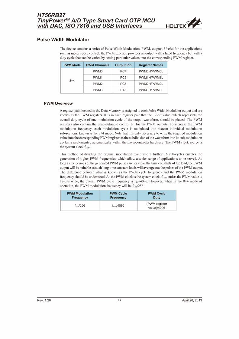
Pulse Width Modulator
The device contains a series of Pulse Width Modulation, PWM, outputs. Useful for the applications
such as motor speed control, the PWM function provides an output with a fixed frequency but with a
duty cycle that can be varied by setting particular values into the corresponding PWM register.
PWM Mode PWM Channels Output Pin Register Names
8+4
PWM0 PC4 PWM0H/PWM0L
PWM1 PC5 PWM1H/PWM1L
PWM2 PC6 PWM2H/PWM2L
PWM3 PA5 PWM3H/PWM3L
PWM Overview
A register pair, located in the Data Memory is assigned to each Pulse Width Modulator output and are
known as the PWM registers. It is in each register pair that the 12-bit value, which represents the
overall duty cycle of one modulation cycle of the output waveform, should be placed. The PWM
registers also contain the enable/disable control bit for the PWM outputs. To increase the PWM
modulation frequency, each modulation cycle is modulated into sixteen individual modulation
sub-sections, known as the 8+4 mode. Note that it is only necessary to write the required modulation
value into the corresponding PWM register as the subdivision of the waveform into its sub-modulation
cycles is implemented automatically within the microcontroller hardware. The PWM clock source is
the system clock fSYS.
This method of dividing the original modulation cycle into a further 16 sub-cycles enables the
generation of higher PWM frequencies, which allow a wider range of applications to be served. As
long as the periods of the generated PWM pulses are less than the time constants of the load, the PWM
output will be suitable as such long time constant loads will average out the pulses of the PWM output.
The difference between what is known as the PWM cycle frequency and the PWM modulation
frequency should be understood. As the PWM clock is the system clock, fSYS, and as the PWM value is
12-bits wide, the overall PWM cycle frequency is fSYS/4096. However, when in the 8+4 mode of
operation, the PWM modulation frequency will be fSYS/256.
PWM Modulation
Frequency
PWM Cycle
Frequency
PWM Cycle
Duty
fSYS/256 fSYS/4096(PWM register
value)/4096
HT56RB27TinyPowerTM A/D Type Smart Card OTP MCUwith DAC, ISO 7816 and USB Interfaces
Rev. 1.20 47 April 26, 2013
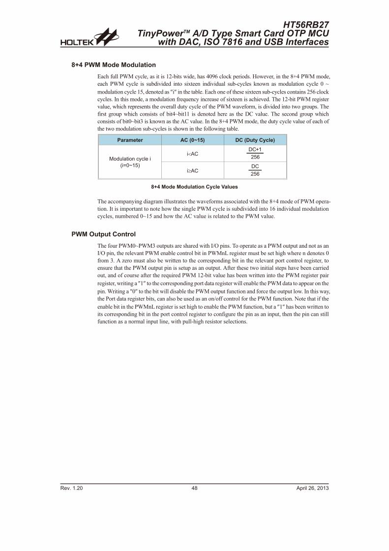
8+4 PWM Mode Modulation
Each full PWM cycle, as it is 12-bits wide, has 4096 clock periods. However, in the 8+4 PWM mode,
each PWM cycle is subdivided into sixteen individual sub-cycles known as modulation cycle 0 ~
modulation cycle 15, denoted as �i� in the table. Each one of these sixteen sub-cycles contains 256 clock
cycles. In this mode, a modulation frequency increase of sixteen is achieved. The 12-bit PWM register
value, which represents the overall duty cycle of the PWM waveform, is divided into two groups. The
first group which consists of bit4~bit11 is denoted here as the DC value. The second group which
consists of bit0~bit3 is known as the AC value. In the 8+4 PWM mode, the duty cycle value of each of
the two modulation sub-cycles is shown in the following table.
Parameter AC (0~15) DC (Duty Cycle)
Modulation cycle i
(i=0~15)
i�ACDC+1
256
i ACDC
256
8+4 Mode Modulation Cycle Values
The accompanying diagram illustrates the waveforms associated with the 8+4 mode of PWM opera-
tion. It is important to note how the single PWM cycle is subdivided into 16 individual modulation
cycles, numbered 0~15 and how the AC value is related to the PWM value.
PWM Output Control
The four PWM0~PWM3 outputs are shared with I/O pins. To operate as a PWM output and not as an
I/O pin, the relevant PWM enable control bit in PWMnL register must be set high where n denotes 0
from 3. A zero must also be written to the corresponding bit in the relevant port control register, to
ensure that the PWM output pin is setup as an output. After these two initial steps have been carried
out, and of course after the required PWM 12-bit value has been written into the PWM register pair
register, writing a �1� to the corresponding port data register will enable the PWM data to appear on the
pin. Writing a �0� to the bit will disable the PWM output function and force the output low. In this way,
the Port data register bits, can also be used as an on/off control for the PWM function. Note that if the
enable bit in the PWMnL register is set high to enable the PWM function, but a �1� has been written to
its corresponding bit in the port control register to configure the pin as an input, then the pin can still
function as a normal input line, with pull-high resistor selections.
Rev. 1.20 48 April 26, 2013
HT56RB27TinyPowerTM A/D Type Smart Card OTP MCU
with DAC, ISO 7816 and USB Interfaces
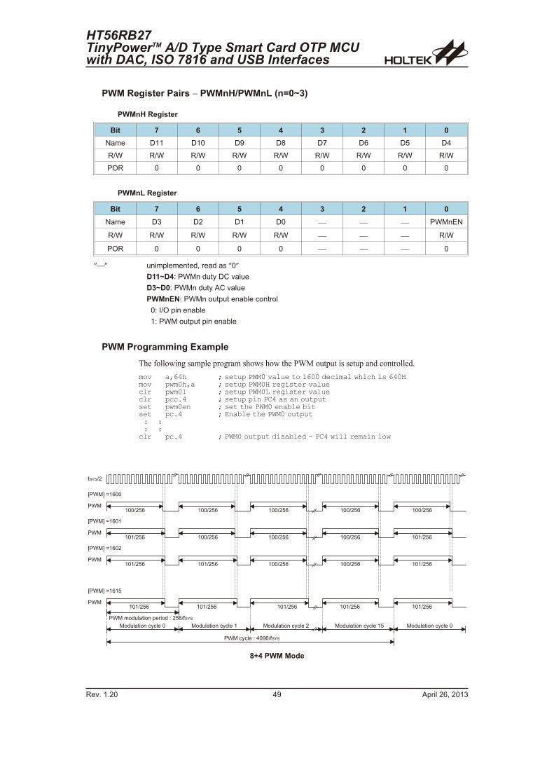
PWM Register Pairs � PWMnH/PWMnL (n=0~3)
PWMnH Register
Bit 7 6 5 4 3 2 1 0
Name D11 D10 D9 D8 D7 D6 D5 D4
R/W R/W R/W R/W R/W R/W R/W R/W R/W
POR 0 0 0 0 0 0 0 0
PWMnL Register
Bit 7 6 5 4 3 2 1 0
Name D3 D2 D1 D0 � � � PWMnEN
R/W R/W R/W R/W R/W � � � R/W
POR 0 0 0 0 � � � 0
��� unimplemented, read as �0�
D11~D4: PWMn duty DC value
D3~D0: PWMn duty AC value
PWMnEN: PWMn output enable control
0: I/O pin enable
1: PWM output pin enable
PWM Programming Example
The following sample program shows how the PWM output is setup and controlled.
mov a,64h ; setup PWM0 value to 1600 decimal which is 640Hmov pwm0h,a ; setup PWM0H register valueclr pwm0l ; setup PWM0L register valueclr pcc.4 ; setup pin PC4 as an outputset pwm0en ; set the PWM0 enable bitset pc.4 ; Enable the PWM0 output: :: :
clr pc.4 ; PWM0 output disabled - PC4 will remain low
HT56RB27TinyPowerTM A/D Type Smart Card OTP MCUwith DAC, ISO 7816 and USB Interfaces
Rev. 1.20 49 April 26, 2013
: # - # = �
� C /
1 � C / 3 � I � * 7 7
1 � C / 3 � I � * 7 �
� C /
1 � C / 3 � I � * 7 �
� C /
1 � C / 3 � I � * � )
� C /
� C / � $ � � � . � ' 7 A * = : # - #
� 7 7 = � ) *
� 7 � = � ) *
� 7 � = � ) *
� 7 � = � ) *
/ ; � � � � � � � $ � � � 7
� C / � � ; � � � � � � � ( � ! � ; � . � � ) * = : # - #
/ ; � � � � � � � $ � � � � / ; � � � � � � � $ � � � � / ; � � � � � � � $ � � � � ) / ; � � � � � � � $ � � � 7
� 7 7 = � ) * � 7 7 = � ) * � 7 7 = � ) *
� 7 � = � ) *
� 7 7 = � ) *
� 7 � = � ) * � 7 � = � ) * � 7 � = � ) *
� 7 7 = � ) *
� 7 7 = � ) * � 7 7 = � ) *
� 7 7 = � ) *
� 7 7 = � ) *
� 7 � = � ) *
� 7 � = � ) *
� 7 � = � ) *
8+4 PWM Mode
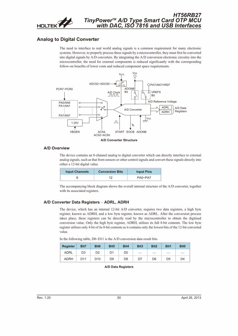
Analog to Digital Converter
The need to interface to real world analog signals is a common requirement for many electronic
systems. However, to properly process these signals by a microcontroller, they must first be converted
into digital signals by A/D converters. By integrating the A/D conversion electronic circuitry into the
microcontroller, the need for external components is reduced significantly with the corresponding
follow-on benefits of lower costs and reduced component space requirements.
A/D Overview
The device contains an 8-channel analog to digital converter which can directly interface to external
analog signals, such as that from sensors or other control signals and convert these signals directly into
either a 12-bit digital value.
Input Channels Conversion Bits Input Pins
8 12 PA0~PA7
The accompanying block diagram shows the overall internal structure of the A/D converter, together
with its associated registers.
A/D Converter Data Registers � ADRL, ADRH
The device, which has an internal 12-bit A/D converter, requires two data registers, a high byte
register, known as ADRH, and a low byte register, known as ADRL. After the conversion process
takes place, these registers can be directly read by the microcontroller to obtain the digitised
conversion value. Only the high byte register, ADRH, utilises its full 8-bit contents. The low byte
register utilises only 4 bit of its 8-bit contents as it contains only the lowest bits of the 12-bit converted
value.
In the following table, D0~D11 is the A/D conversion data result bits.
Register Bit7 Bit6 Bit5 Bit4 Bit3 Bit2 Bit1 Bit0
ADRL D3 D2 D1 D0 � � � �
ADRH D11 D10 D9 D8 D7 D6 D5 D4
A/D Data Registers
Rev. 1.20 50 April 26, 2013
HT56RB27TinyPowerTM A/D Type Smart Card OTP MCU
with DAC, ISO 7816 and USB Interfaces
, = � � � � 9 � ! � � !
� , 7 = , 4 7� , � = , 4 �
� , 5 = , 4 5
, = � � � : � ! � � � � � � � � % �
, � +
, � 2
, = � � � � � � � % � � � � ! �
� 8 @ � 4 # � , � � � 8 , � 4 8
� # #
� , 5 = , 4 5 = � � �, � � # � G , � � # 7
: # - #
� � 5 G � � 7
, � # ' 0, � # � G , � # 7
� � � ) �
, = � � � � "
� � �
, � 4 88 � � � � � #
8 � �
� � � � 4� 4 I 7 G ) �
A/D Converter Structure
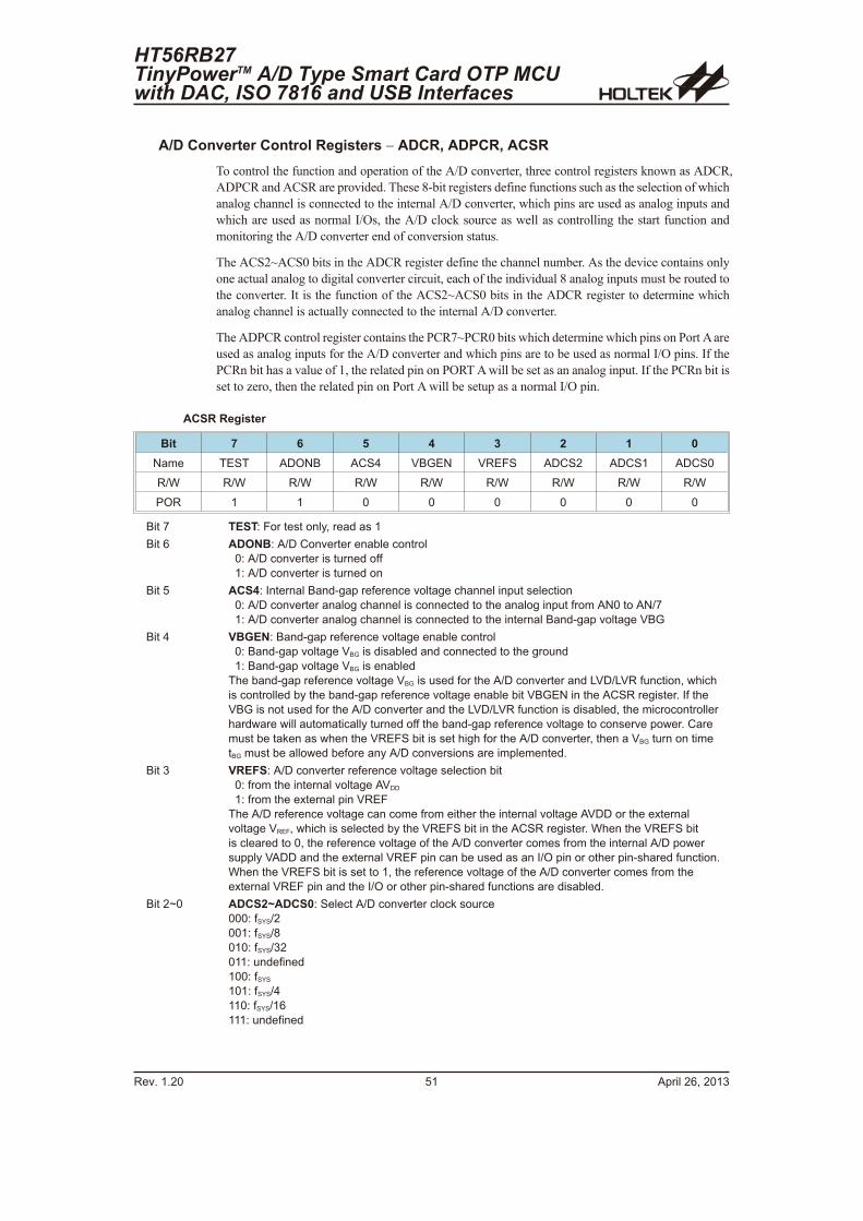
A/D Converter Control Registers � ADCR, ADPCR, ACSR
To control the function and operation of the A/D converter, three control registers known as ADCR,
ADPCR and ACSR are provided. These 8-bit registers define functions such as the selection of which
analog channel is connected to the internal A/D converter, which pins are used as analog inputs and
which are used as normal I/Os, the A/D clock source as well as controlling the start function and
monitoring the A/D converter end of conversion status.
The ACS2~ACS0 bits in the ADCR register define the channel number. As the device contains only
one actual analog to digital converter circuit, each of the individual 8 analog inputs must be routed to
the converter. It is the function of the ACS2~ACS0 bits in the ADCR register to determine which
analog channel is actually connected to the internal A/D converter.
The ADPCR control register contains the PCR7~PCR0 bits which determine which pins on Port A are
used as analog inputs for the A/D converter and which pins are to be used as normal I/O pins. If the
PCRn bit has a value of 1, the related pin on PORT A will be set as an analog input. If the PCRn bit is
set to zero, then the related pin on Port A will be setup as a normal I/O pin.
ACSR Register
Bit 7 6 5 4 3 2 1 0
Name TEST ADONB ACS4 VBGEN VREFS ADCS2 ADCS1 ADCS0
R/W R/W R/W R/W R/W R/W R/W R/W R/W
POR 1 1 0 0 0 0 0 0
Bit 7 TEST: For test only, read as 1
Bit 6 ADONB: A/D Converter enable control
0: A/D converter is turned off
1: A/D converter is turned on
Bit 5 ACS4: Internal Band-gap reference voltage channel input selection
0: A/D converter analog channel is connected to the analog input from AN0 to AN/7
1: A/D converter analog channel is connected to the internal Band-gap voltage VBG
Bit 4 VBGEN: Band-gap reference voltage enable control
0: Band-gap voltage VBG is disabled and connected to the ground
1: Band-gap voltage VBG is enabled
The band-gap reference voltage VBG is used for the A/D converter and LVD/LVR function, which
is controlled by the band-gap reference voltage enable bit VBGEN in the ACSR register. If the
VBG is not used for the A/D converter and the LVD/LVR function is disabled, the microcontroller
hardware will automatically turned off the band-gap reference voltage to conserve power. Care
must be taken as when the VREFS bit is set high for the A/D converter, then a VBG turn on time
tBG must be allowed before any A/D conversions are implemented.
Bit 3 VREFS: A/D converter reference voltage selection bit
0: from the internal voltage AVDD
1: from the external pin VREF
The A/D reference voltage can come from either the internal voltage AVDD or the external
voltage VREF, which is selected by the VREFS bit in the ACSR register. When the VREFS bit
is cleared to 0, the reference voltage of the A/D converter comes from the internal A/D power
supply VADD and the external VREF pin can be used as an I/O pin or other pin-shared function.
When the VREFS bit is set to 1, the reference voltage of the A/D converter comes from the
external VREF pin and the I/O or other pin-shared functions are disabled.
Bit 2~0 ADCS2~ADCS0: Select A/D converter clock source
000: fSYS/2
001: fSYS/8
010: fSYS/32
011: undefined
100: fSYS
101: fSYS/4
110: fSYS/16
111: undefined
HT56RB27TinyPowerTM A/D Type Smart Card OTP MCUwith DAC, ISO 7816 and USB Interfaces
Rev. 1.20 51 April 26, 2013
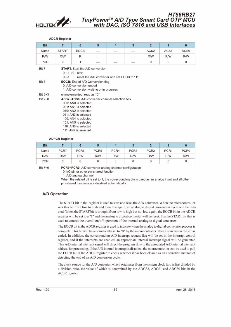
ADCR Register
Bit 7 6 5 4 3 2 1 0
Name START EOCB � � � ACS2 ACS1 ACS0
R/W R/W R � � � R/W R/W R/W
POR 0 1 � � � 0 0 0
Bit 7 START: Start the A/D conversion
0�1�0 : start
0�1 : reset the A/D converter and set EOCB to �1�
Bit 6 EOCB: End of A/D Conversion flag
0: A/D conversion ended
1: A/D conversion waiting or in progress
Bit 5~3 unimplemented, read as �0�
Bit 2~0 ACS2~ACS0: A/D converter channel selection bits
000: AN0 is selected
001: AN1 is selected
010: AN2 is selected
011: AN3 is selected
100: AN4 is selected
101: AN5 is selected
110: AN6 is selected
111: AN7 is selected
ADPCR Register
Bit 7 6 5 4 3 2 1 0
Name PCR7 PCR6 PCR5 PCR4 PCR3 PCR2 PCR1 PCR0
R/W R/W R/W R/W R/W R/W R/W R/W R/W
POR 0 0 0 0 0 0 0 0
Bit 7~0 PCR7~PCR0: A/D converter analog channel configuration
0: I/O pin or other pin-shared function
1: A/D analog channel
When the related bit is set to 1, the corresponding pin is used as an analog input and all other
pin-shared functions are disabled automatically.
A/D Operation
The START bit in the register is used to start and reset the A/D converter. When the microcontroller
sets this bit from low to high and then low again, an analog to digital conversion cycle will be initi-
ated. When the START bit is brought from low to high but not low again, the EOCB bit in the ADCR
register will be set to a �1� and the analog to digital converter will be reset. It is the START bit that is
used to control the overall on/off operation of the internal analog to digital converter.
The EOCB bit in the ADCR register is used to indicate when the analog to digital conversion process is
complete. This bit will be automatically set to �0� by the microcontroller after a conversion cycle has
ended. In addition, the corresponding A/D interrupt request flag will be set in the interrupt control
register, and if the interrupts are enabled, an appropriate internal interrupt signal will be generated.
This A/D internal interrupt signal will direct the program flow to the associated A/D internal interrupt
address for processing. If the A/D internal interrupt is disabled, the microcontroller can be used to poll
the EOCB bit in the ADCR register to check whether it has been cleared as an alternative method of
detecting the end of an A/D conversion cycle.
The clock source for the A/D converter, which originates from the system clock fSYS, is first divided by
a division ratio, the value of which is determined by the ADCS2, ADCS1 and ADCS0 bits in the
ACSR register.
Rev. 1.20 52 April 26, 2013
HT56RB27TinyPowerTM A/D Type Smart Card OTP MCU
with DAC, ISO 7816 and USB Interfaces
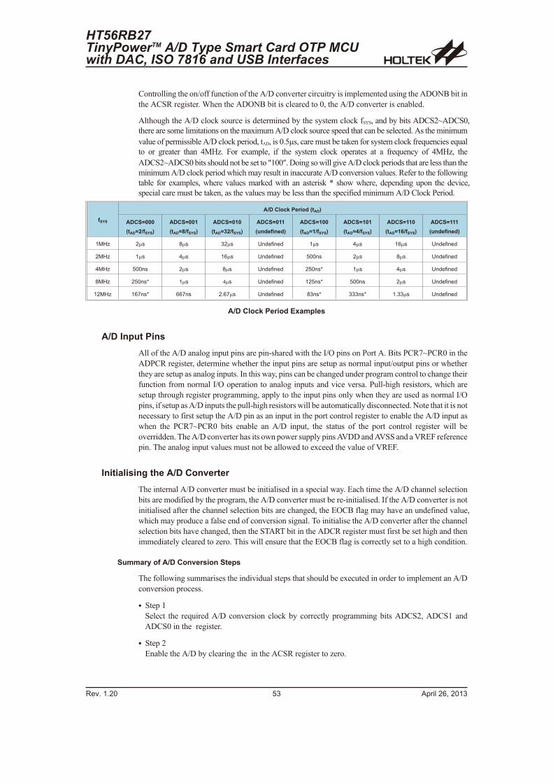
Controlling the on/off function of the A/D converter circuitry is implemented using the ADONB bit in
the ACSR register. When the ADONB bit is cleared to 0, the A/D converter is enabled.
Although the A/D clock source is determined by the system clock fSYS, and by bits ADCS2~ADCS0,
there are some limitations on the maximum A/D clock source speed that can be selected. As the minimum
value of permissible A/D clock period, tAD, is 0.5�s, care must be taken for system clock frequencies equal
to or greater than 4MHz. For example, if the system clock operates at a frequency of 4MHz, the
ADCS2~ADCS0 bits should not be set to �100�. Doing so will give A/D clock periods that are less than the
minimum A/D clock period which may result in inaccurate A/D conversion values. Refer to the following
table for examples, where values marked with an asterisk * show where, depending upon the device,
special care must be taken, as the values may be less than the specified minimum A/D Clock Period.
fSYS
A/D Clock Period (tAD)
ADCS=000
(tAD=2/fSYS)
ADCS=001
(tAD=8/fSYS)
ADCS=010
(tAD=32/fSYS)
ADCS=011
(undefined)
ADCS=100
(tAD=1/fSYS)
ADCS=101
(tAD=4/fSYS)
ADCS=110
(tAD=16/fSYS)
ADCS=111
(undefined)
1MHz 2�s 8�s 32�s Undefined 1�s 4�s 16�s Undefined
2MHz 1�s 4�s 16�s Undefined 500ns 2�s 8�s Undefined
4MHz 500ns 2�s 8�s Undefined 250ns* 1�s 4�s Undefined
8MHz 250ns* 1�s ��s Undefined 125ns* 500ns 2�s Undefined
12MHz 167ns* 667ns 2.67�s Undefined 83ns* 333ns* 1.33�s Undefined
A/D Clock Period Examples
A/D Input Pins
All of the A/D analog input pins are pin-shared with the I/O pins on Port A. Bits PCR7~PCR0 in the
ADPCR register, determine whether the input pins are setup as normal input/output pins or whether
they are setup as analog inputs. In this way, pins can be changed under program control to change their
function from normal I/O operation to analog inputs and vice versa. Pull-high resistors, which are
setup through register programming, apply to the input pins only when they are used as normal I/O
pins, if setup as A/D inputs the pull-high resistors will be automatically disconnected. Note that it is not
necessary to first setup the A/D pin as an input in the port control register to enable the A/D input as
when the PCR7~PCR0 bits enable an A/D input, the status of the port control register will be
overridden. The A/D converter has its own power supply pins AVDD and AVSS and a VREF reference
pin. The analog input values must not be allowed to exceed the value of VREF.
Initialising the A/D Converter
The internal A/D converter must be initialised in a special way. Each time the A/D channel selection
bits are modified by the program, the A/D converter must be re-initialised. If the A/D converter is not
initialised after the channel selection bits are changed, the EOCB flag may have an undefined value,
which may produce a false end of conversion signal. To initialise the A/D converter after the channel
selection bits have changed, then the START bit in the ADCR register must first be set high and then
immediately cleared to zero. This will ensure that the EOCB flag is correctly set to a high condition.
Summary of A/D Conversion Steps
The following summarises the individual steps that should be executed in order to implement an A/D
conversion process.
� Step 1
Select the required A/D conversion clock by correctly programming bits ADCS2, ADCS1 and
ADCS0 in the register.
� Step 2
Enable the A/D by clearing the in the ACSR register to zero.
HT56RB27TinyPowerTM A/D Type Smart Card OTP MCUwith DAC, ISO 7816 and USB Interfaces
Rev. 1.20 53 April 26, 2013

� Step 3
Select which channel is to be connected to the internal A/D converter by correctly programming the
ACS2~ACS0 bits which are also contained in the register.
� Step 4
Select which pins on the I/O port are to be used as A/D inputs and configure them as A/D input pins
by correctly programming the PCR7~PCR0 bits in the ADPCR register.
� Step 5
If the interrupts are to be used, the interrupt control registers must be correctly configured to ensure
the A/D converter interrupt function is active. The master interrupt control bit, EMI, in the INTC0
interrupt control register must be set to �1� and the A/D converter interrupt enable bit, EADI, in the
INTC2 register must also be set to �1�.
� Step 6
The analog to digital conversion process can now be initialised by setting the START bit in the
ADCR register from �0� to �1� and then to �0� again. Note that this bit should have been originally
set to �0�.
� Step 7
To check when the analog to digital conversion process is complete, the EOCB bit in the ADCR
register can be polled. The conversion process is complete when this bit goes low. When this occurs
the A/D data registers ADRL and ADRH can be read to obtain the conversion value. As an
alternative method if the interrupts are enabled and the stack is not full, the program can wait for an
A/D interrupt to occur.
Note When checking for the end of the conversion process, if the method of polling the bit in the ADCR
register is used, the interrupt enable step above can be omitted.
The accompanying diagram shows graphically the various stages involved in an analog to digital
conversion process and its associated timing.
The setting up and operation of the A/D converter function is fully under the control of the application
program as there are no configuration options associated with the A/D converter. After an A/D
conversion process has been initiated by the application program, the microcontroller internal hardware
will begin to carry out the conversion, during which time the program can continue with other functions.
The time taken for the A/D conversion is 16tAD where tAD is equal to the A/D clock period.
Rev. 1.20 54 April 26, 2013
HT56RB27TinyPowerTM A/D Type Smart Card OTP MCU
with DAC, ISO 7816 and USB Interfaces
� , � �
, = � � � 9 � ! � � � � � � � �
7 7 7 7 � 7 7 7 7 8
� � � 8
7 7 7 7 � 7 � 7 7 8
7 � 7 8
# � , �
� � 8
� � � G� � 7
, � # � G, � # 7
� ? � ! � � � � � �
� � ; � : � , = � � 9 � ! � � �� . � � � : � � � � ( ! � � � : � % � ! � � � �
� . � # � � � � � � � � � % � � � � � � �
, = � � � " � � � � � � < � � : � $ � 0 � : # - # = � 0 � : # - # = ' 0 � : # - # = 6 0 � : # - # = � * � ! � : # - # = & �� , � � # I ' � , �
� , � � I � � , � � # � � J � , � K � � I < � � � � � � � : � , � � � ! � � � � � � �
4 � � . �
# � � ! � � : � , = � � 9 � ! � � �
� � � � � , = � � 9 � ! � � !
, = � � � � � ( � � � % � � � � �� � � , � � # �
7 7 7 8
# � � ! � � : � , = � � 9 � ! � � �
� � � � � , = � � 9 � ! � � !
7 7 7 7 � 7 � 7 � 8
7 7 � 8
# � � ! � � : � , = � � 9 � ! � � �
� � � � � , = � � 9 � ! � � !
� � ; � : � , = � � 9 � ! � � �
, = � � � � � ( � � � % � � � � �� � � , � � # �
7 7 7 7 � 7 7 7 7 8
� � � 8
, � � � � ; � � � 4
, � 4 8
: : : : � �
� 4 � # �
� , � �
, = � � � 9 � ! � � � � � � � �
A/D Conversion Timing
Programming Considerations
The A/D converter can be powered down by setting the ADONB bit in ACSR register to reduce power
consumption. It is an important ability for some applications such as battery powered or handheld
appliance.
Another important programming consideration is that when the A/D channel selection bits change
value, the A/D converter must be re-initialised. This is achieved by pulsing the START bit in the
ADCR register immediately after the channel selection bits have changed state. The exception to this
is where the channel selection bits are all cleared, in which case the A/D converter is not required to be
re-initialised.
A/D Programming Example
The following two programming examples illustrate how to setup and implement an A/D conversion.
In the first example, the method of polling the EOCB bit in the ADCR register is used to detect when
the conversion cycle is complete, whereas in the second example, the A/D interrupt is used to
determine when the conversion is complete.
Example: using an EOCB polling method to detect the end of conversion
clr EADI ; disable ADC interruptmov a,00000001Bmov ACSR,a ; select fSYS/8 as A/D clock and turn on ADONB bitmov a,0FH ; setup ADPCR register to configure Port A pin PA0~PA3mov ADPCR,a, ; as A/D inputsmov a,00H ; and select AN0 to be connected to the A/D converterMov ADCR,a :
: ; As the Port A channel bits have changed the; following START; signal (0-1-0) must be issued; instruction cycles
:Start_conversion:
clr STARTset START ; reset A/Dclr START ; start A/D
Polling_:sz EOCB ; poll the ADCR register EOCB bit to detect end
; of A/D conversionjmp polling_EOC ; continue pollingmov a,ADRL ; read low byte conversion result valuemov adrl_buffer,a ; save result to user defined registermov a,ADRH ; read high byte conversion result valuemov adrh_buffer,a ; save result to user defined register
:jmp start_conversion ; start next A/D conversion
HT56RB27TinyPowerTM A/D Type Smart Card OTP MCUwith DAC, ISO 7816 and USB Interfaces
Rev. 1.20 55 April 26, 2013
Example: using the interrupt method to detect the end of conversion
clr EADI ; disable ADC interruptmov a,00000001Bmov ACSR,a ; select fSYS/8 as A/D clock and turn on ADONB bitmov ADPCR,a ; setup ADPCR register to configure Port A pin PA0~PA3
; as A/D inputsmov ADCR,a ; and select AN0 to be connected to the A/D converter
:; As the Port A channel bits have changed the; following START signal(0-1-0) must be issued;
:Start_conversion:
clr STARTset START ; reset A/Dclr START ; start A/Dclr ADF ; clear ADC interrupt request flagset EADI ; enable ADC interruptset EMI ; enable global interrupt
:::
; ADC interrupt service routineADC_:
mov acc_stack,a ; save ACC to user defined memorymov a,STATUSmov status_stack,a ; save STATUS to user defined memory
::
mov a,ADRL ; read low byte conversion result valuemov adrl_buffer,a ; save result to user defined registermov a,ADRH ; read high byte conversion result valuemov adrh_buffer,a ; save result to user defined register
::
EXIT__ISR:mov a,status_stackmov STATUS,a ; restore STATUS from user defined memorymov a,acc_stack ; restore ACC from user defined memoryclr ADF ; clear ADC interrupt flagreti
Rev. 1.20 56 April 26, 2013
HT56RB27TinyPowerTM A/D Type Smart Card OTP MCU
with DAC, ISO 7816 and USB Interfaces
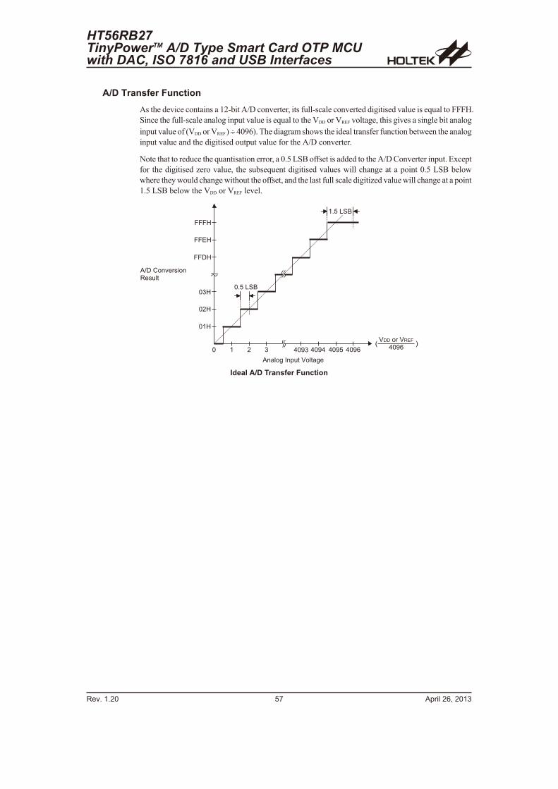
A/D Transfer Function
As the device contains a 12-bit A/D converter, its full-scale converted digitised value is equal to FFFH.
Since the full-scale analog input value is equal to the VDD or VREF voltage, this gives a single bit analog
input value of (VDD or VREF) � 4096). The diagram shows the ideal transfer function between the analog
input value and the digitised output value for the A/D converter.
Note that to reduce the quantisation error, a 0.5 LSB offset is added to the A/D Converter input. Except
for the digitised zero value, the subsequent digitised values will change at a point 0.5 LSB below
where they would change without the offset, and the last full scale digitized value will change at a point
1.5 LSB below the VDD or VREF level.
HT56RB27TinyPowerTM A/D Type Smart Card OTP MCUwith DAC, ISO 7816 and USB Interfaces
Rev. 1.20 57 April 26, 2013
� � � 2
� � � � � � � � � � � � � � � � � � � � �
, = � � � � 9 � ! � � � � � � � �
� � � 2
� � � 2
7 & 2
7 � 2
7 � 2
7 � ) � + # 8
7 � � & ' 7 A & ' 7 A ' ' 7 A ) ' 7 A *
, � � � % � � � ( � � � � � � � % �
� � ) � + # 8
� � � � ! � � � �
' 7 A *
Ideal A/D Transfer Function
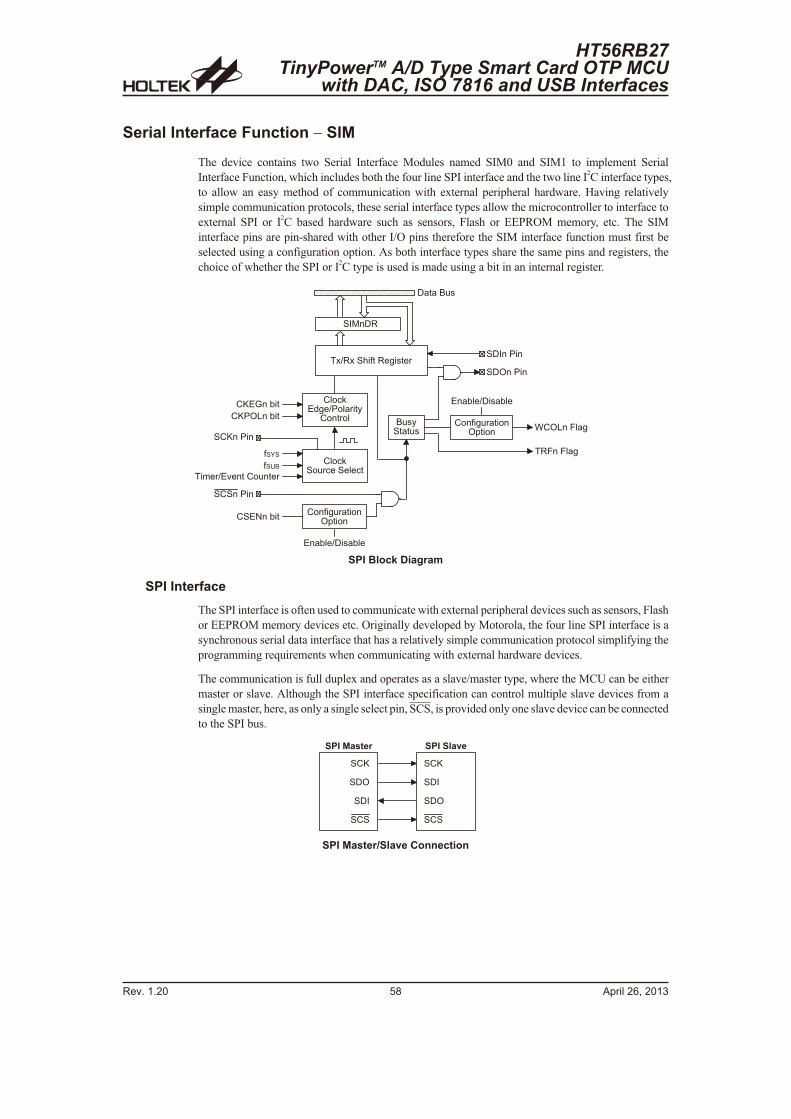
Serial Interface Function � SIM
The device contains two Serial Interface Modules named SIM0 and SIM1 to implement Serial
Interface Function, which includes both the four line SPI interface and the two line I2C interface types,
to allow an easy method of communication with external peripheral hardware. Having relatively
simple communication protocols, these serial interface types allow the microcontroller to interface to
external SPI or I2C based hardware such as sensors, Flash or EEPROM memory, etc. The SIM
interface pins are pin-shared with other I/O pins therefore the SIM interface function must first be
selected using a configuration option. As both interface types share the same pins and registers, the
choice of whether the SPI or I2C type is used is made using a bit in an internal register.
SPI Interface
The SPI interface is often used to communicate with external peripheral devices such as sensors, Flash
or EEPROM memory devices etc. Originally developed by Motorola, the four line SPI interface is a
synchronous serial data interface that has a relatively simple communication protocol simplifying the
programming requirements when communicating with external hardware devices.
The communication is full duplex and operates as a slave/master type, where the MCU can be either
master or slave. Although the SPI interface specification can control multiple slave devices from a
single master, here, as only a single select pin, SCS, is provided only one slave device can be connected
to the SPI bus.
Rev. 1.20 58 April 26, 2013
HT56RB27TinyPowerTM A/D Type Smart Card OTP MCU
with DAC, ISO 7816 and USB Interfaces
� � � � � � � � � � � � � � � � �
# � B
# �
# � �
# � #
# � B
# � �
# �
# � #
SPI Master/Slave Connection
� � � � � 8 � �
# � � � � � � �
# � � � � � �
# � / � �
� � = � � # � � : � � � % � � � � !
8 � � $# � � � � �
� � : � % � ! � � � � ( � � �
� � � � � � � %
� � � < � � = � � � � < � �
C � + � � � � � %
� � "� ; % � = � � � ! � � $
� � � ! �
� � "# � ! � � # � � � �
: # - #
: # > 8
� � � � ! = � 9 � � � � � � � � � !
# � B � � � � �
# � # � � � � �
� � : � % � ! � � � � ( � � �
� # � 4 � � < � �
� � � < � � = � � � � < � �
� B � @ � � < � �
� B � + � � < � �
SPI Block Diagram
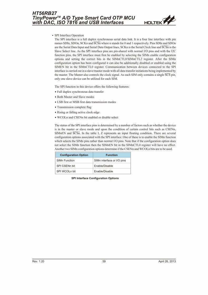
� SPI Interface Operation
The SPI interface is a full duplex synchronous serial data link. It is a four line interface with pin
names SDIn, SDOn, SCKn and SCSn where n stands for 0 and 1 respectively. Pins SDIn and SDOn
are the Serial Data Input and Serial Data Output lines, SCKn is the Serial Clock line and SCSn is the
Slave Select line. As the SPI interface pins are pin-shared with normal I/O pins and with the I2C
function pins, the SPI interface must first be enabled by selecting the SIMn enable configuration
options and setting the correct bits in the SIMnCTL0/SIMnCTL2 register. After the SIMn
configuration option has been configured it can also be additionally disabled or enabled using the
SIMEN bit in the SIMnCTL0 register. Communication between devices connected to the SPI
interface is carried out in a slave/master mode with all data transfer initiations being implemented by
the master. The Master also controls the clock signal. As each SIM only contains a single SCS pin,
only one slave device can be utilized for each SIM.
The SPI function in this device offers the following features:
� Full duplex synchronous data transfer
� Both Master and Slave modes
� LSB first or MSB first data transmission modes
� Transmission complete flag
� Rising or falling active clock edge
� WCOLn and CSENn bit enabled or disable select
The status of the SPI interface pins is determined by a number of factors such as whether the device
is in the master or slave mode and upon the condition of certain control bits such as CSENn,
SIMnEN and SCSn. In the table I, Z represents an input floating condition. There are several
configuration options associated with the SPI interface. One of these is to enable the SIMn function
which selects the SIMn pins rather than normal I/O pins. Note that if the configuration option does
not select the SIMn function then the SIMnEN bit in the SIMnCTL0 register will have no effect.
Another two SIMn configuration options determine if the CSENn and WCOLn bits are to be used.
Configuration Option Function
SIMn Function SIMn interface or I/O pins
SPI CSENn bit Enable/Disable
SPI WCOLn bit Enable/Disable
SPI Interface Configuration Options
HT56RB27TinyPowerTM A/D Type Smart Card OTP MCUwith DAC, ISO 7816 and USB Interfaces
Rev. 1.20 59 April 26, 2013
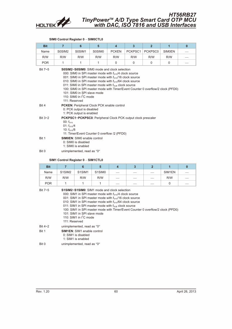
SIM0 Control Register 0 � SIM0CTL0
Bit 7 6 5 4 3 2 1 0
Name S0SIM2 S0SIM1 S0SIM0 PCKEN PCKPSC1 PCKPSC0 SIM0EN �
R/W R/W R/W R/W R/W R/W R/W R/W �
POR 1 1 1 0 0 0 0 �
Bit 7~5 S0SIM2~S0SIM0: SIM0 mode and clock selection
000: SIM0 in SPI master mode with fSYS/4 clock source
001: SIM0 in SPI master mode with fSYS/16 clock source
010: SIM0 in SPI master mode with fSYS/64 clock source
011: SIM0 in SPI master mode with fSUB clock source
100: SIM0 in SPI master mode with Timer/Event Counter 0 overflow/2 clock (PFD0)
101: SIM0 in SPI slave mode
110: SIM0 in I2C mode
111: Reserved
Bit 4 PCKEN: Peripheral Clock PCK enable control
0: PCK output is disabled
1: PCK output is enabled
Bit 3~2 PCKPSC1~PCKPSC0: Peripheral Clock PCK output clock prescaler
00: fSYS
01: fSYS/4
10: fSYS/8
11: Timer/Event Counter 0 overflow /2 (PFD0)
Bit 1 SIM0EN: SIM0 enable control
0: SIM0 is disabled
1: SIM0 is enabled
Bit 0 unimplemented, read as �0�
SIM1 Control Register 0 � SIM1CTL0
Bit 7 6 5 4 3 2 1 0
Name S1SIM2 S1SIM1 S1SIM0 � � � SIM1EN �
R/W R/W R/W R/W � � � R/W �
POR 1 1 1 � � � 0 �
Bit 7~5 S1SIM2~S1SIM0: SIM1 mode and clock selection
000: SIM1 in SPI master mode with fSYS/4 clock source
001: SIM1 in SPI master mode with fSYS/16 clock source
010: SIM1 in SPI master mode with fSYS/64 clock source
011: SIM1 in SPI master mode with fSUB clock source
100: SIM1 in SPI master mode with Timer/Event Counter 0 overflow/2 clock (PFD0)
101: SIM1 in SPI slave mode
110: SIM1 in I2C mode
111: Reserved
Bit 4~2 unimplemented, read as �0�
Bit 1 SIM1EN: SIM1 enable control
0: SIM1 is disabled
1: SIM1 is enabled
Bit 0 unimplemented, read as �0�
Rev. 1.20 60 April 26, 2013
HT56RB27TinyPowerTM A/D Type Smart Card OTP MCU
with DAC, ISO 7816 and USB Interfaces
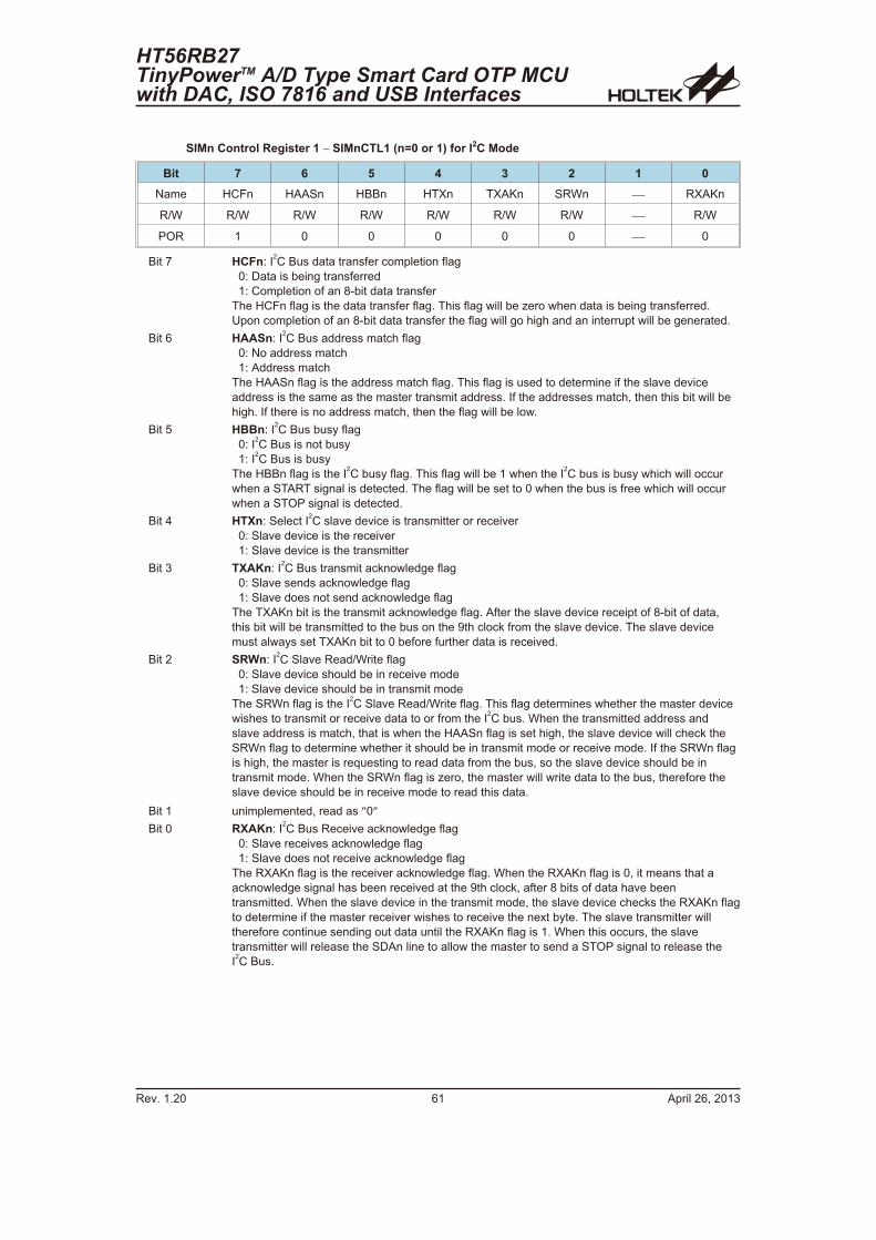
SIMn Control Register 1 � SIMnCTL1 (n=0 or 1) for I2C Mode
Bit 7 6 5 4 3 2 1 0
Name HCFn HAASn HBBn HTXn TXAKn SRWn � RXAKn
R/W R/W R/W R/W R/W R/W R/W � R/W
POR 1 0 0 0 0 0 � 0
Bit 7 HCFn: I2C Bus data transfer completion flag
0: Data is being transferred
1: Completion of an 8-bit data transfer
The HCFn flag is the data transfer flag. This flag will be zero when data is being transferred.
Upon completion of an 8-bit data transfer the flag will go high and an interrupt will be generated.
Bit 6 HAASn: I2C Bus address match flag
0: No address match
1: Address match
The HAASn flag is the address match flag. This flag is used to determine if the slave device
address is the same as the master transmit address. If the addresses match, then this bit will be
high. If there is no address match, then the flag will be low.
Bit 5 HBBn: I2C Bus busy flag
0: I2C Bus is not busy
1: I2C Bus is busy
The HBBn flag is the I2C busy flag. This flag will be 1 when the I
2C bus is busy which will occur
when a START signal is detected. The flag will be set to 0 when the bus is free which will occur
when a STOP signal is detected.
Bit 4 HTXn: Select I2C slave device is transmitter or receiver
0: Slave device is the receiver
1: Slave device is the transmitter
Bit 3 TXAKn: I2C Bus transmit acknowledge flag
0: Slave sends acknowledge flag
1: Slave does not send acknowledge flag
The TXAKn bit is the transmit acknowledge flag. After the slave device receipt of 8-bit of data,
this bit will be transmitted to the bus on the 9th clock from the slave device. The slave device
must always set TXAKn bit to 0 before further data is received.
Bit 2 SRWn: I2C Slave Read/Write flag
0: Slave device should be in receive mode
1: Slave device should be in transmit mode
The SRWn flag is the I2C Slave Read/Write flag. This flag determines whether the master device
wishes to transmit or receive data to or from the I2C bus. When the transmitted address and
slave address is match, that is when the HAASn flag is set high, the slave device will check the
SRWn flag to determine whether it should be in transmit mode or receive mode. If the SRWn flag
is high, the master is requesting to read data from the bus, so the slave device should be in
transmit mode. When the SRWn flag is zero, the master will write data to the bus, therefore the
slave device should be in receive mode to read this data.
Bit 1 unimplemented, read as �0�
Bit 0 RXAKn: I2C Bus Receive acknowledge flag
0: Slave receives acknowledge flag
1: Slave does not receive acknowledge flag
The RXAKn flag is the receiver acknowledge flag. When the RXAKn flag is 0, it means that a
acknowledge signal has been received at the 9th clock, after 8 bits of data have been
transmitted. When the slave device in the transmit mode, the slave device checks the RXAKn flag
to determine if the master receiver wishes to receive the next byte. The slave transmitter will
therefore continue sending out data until the RXAKn flag is 1. When this occurs, the slave
transmitter will release the SDAn line to allow the master to send a STOP signal to release the
I2C Bus.
HT56RB27TinyPowerTM A/D Type Smart Card OTP MCUwith DAC, ISO 7816 and USB Interfaces
Rev. 1.20 61 April 26, 2013
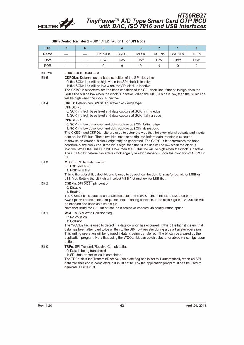
SIMn Control Register 2 � SIMnCTL2 (n=0 or 1) for SPI Mode
Bit 7 6 5 4 3 2 1 0
Name � � CKPOLn CKEG MLSn CSENn WCOLn TRFn
R/W � � R/W R/W R/W R/W R/W R/W
POR � � 0 0 0 0 0 0
Bit 7~6 undefined bit, read as 0
Bit 5 CKPOLn: Determines the base condition of the SPI clock line
0: the SCKn line will be high when the SPI clock is inactive
1: the SCKn line will be low when the SPI clock is inactive
The CKPOLn bit determines the base condition of the SPI clock line, if the bit is high, then the
SCKn line will be low when the clock is inactive. When the CKPOLn bit is low, then the SCKn line
will be high when the clock is inactive.
Bit 4 CKEG: Determines SPI SCKn active clock edge type
CKPOLn=0
0: SCKn is high base level and data capture at SCKn rising edge
1: SCKn is high base level and data capture at SCKn falling edge
CKPOLn=1
0: SCKn is low base level and data capture at SCKn falling edge
1: SCKn is low base level and data capture at SCKn rising edge
The CKEGn and CKPOLn bits are used to setup the way that the clock signal outputs and inputs
data on the SPI bus. These two bits must be configured before data transfer is executed
otherwise an erroneous clock edge may be generated. The CKPOLn bit determines the base
condition of the clock line. If the bit is high, then the SCKn line will be low when the clock is
inactive. When the CKPOLn bit is low, then the SCKn line will be high when the clock is inactive.
The CKEGn bit determines active clock edge type which depends upon the condition of CKPOLn
bit.
Bit 3 MLSn: SPI Data shift order
0: LSB shift first
1: MSB shift first
This is the data shift select bit and is used to select how the data is transferred, either MSB or
LSB first. Setting the bit high will select MSB first and low for LSB first.
Bit 2 CSENn: SPI SCSn pin control
0: Disable
1: Enable
The CSENn bit is used as an enable/disable for the SCSn pin. If this bit is low, then the
SCSn pin will be disabled and placed into a floating condition. If the bit is high the SCSn pin will
be enabled and used as a select pin.
Note that using the CSENn bit can be disabled or enabled via configuration option.
Bit 1 WCOLn: SPI Write Collision flag
0: No collision
1: Collision
The WCOLn flag is used to detect if a data collision has occurred. If this bit is high it means that
data has been attempted to be written to the SIMnDR register during a data transfer operation.
This writing operation will be ignored if data is being transferred. The bit can be cleared by the
application program. Note that using the WCOLn bit can be disabled or enabled via configuration
option.
Bit 0 TRFn: SPI Transmit/Receive Complete flag
0: Data is being transferred
1: SPI data transmission is completed
The TRFn bit is the Transmit/Receive Complete flag and is set to 1 automatically when an SPI
data transmission is completed, but must set to 0 by the application program. It can be used to
generate an interrupt.
Rev. 1.20 62 April 26, 2013
HT56RB27TinyPowerTM A/D Type Smart Card OTP MCU
with DAC, ISO 7816 and USB Interfaces
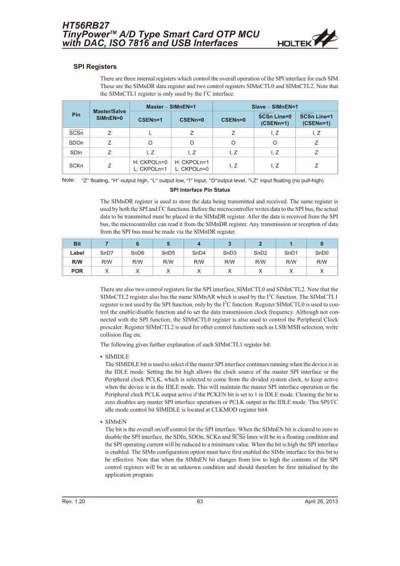
SPI Registers
There are three internal registers which control the overall operation of the SPI interface for each SIM.
These are the SIMnDR data register and two control registers SIMnCTL0 and SIMnCTL2. Note that
the SIMnCTL1 register is only used by the I2C interface.
PinMaster/Salve
SIMnEN=0
Master � SIMnEN=1 Slave � SIMnEN=1
CSENn=1 CSENn=0 CSENn=0SCSn Line=0
(CSENn=1)
SCSn Line=1
(CSENn=1)
SCSn Z L Z Z I, Z I, Z
SDOn Z O O O O Z
SDIn Z I, Z I, Z I, Z I, Z Z
SCKn ZH: CKPOLn=0
L: CKPOLn=1
H: CKPOLn=1
L: CKPOLn=0I, Z I, Z Z
Note: �Z� floating, �H� output high, �L� output low, �I� Input, �O�output level, �I,Z� input floating (no pull-high)
SPI Interface Pin Status
The SIMnDR register is used to store the data being transmitted and received. The same register is
used by both the SPI and I2C functions. Before the microcontroller writes data to the SPI bus, the actual
data to be transmitted must be placed in the SIMnDR register. After the data is received from the SPI
bus, the microcontroller can read it from the SIMnDR register. Any transmission or reception of data
from the SPI bus must be made via the SIMnDR register.
Bit 7 6 5 4 3 2 1 0
Label SnD7 SnD6 SnD5 SnD4 SnD3 SnD2 SnD1 SnD0
R/W R/W R/W R/W R/W R/W R/W R/W R/W
POR X X X X X X X X
There are also two control registers for the SPI interface, SIMnCTL0 and SIMnCTL2. Note that the
SIMnCTL2 register also has the name SIMnAR which is used by the I2C function. The SIMnCTL1
register is not used by the SPI function, only by the I2C function. Register SIMnCTL0 is used to con-
trol the enable/disable function and to set the data transmission clock frequency. Although not con-
nected with the SPI function, the SIMnCTL0 register is also used to control the Peripheral Clock
prescaler. Register SIMnCTL2 is used for other control functions such as LSB/MSB selection, write
collision flag etc.
The following gives further explanation of each SIMnCTL1 register bit:
� SIMIDLE
The SIMIDLE bit is used to select if the master SPI interface continues running when the device is in
the IDLE mode. Setting the bit high allows the clock source of the master SPI interface or the
Peripheral clock PCLK, which is selected to come from the divided system clock, to keep active
when the device is in the IDLE mode. This will maintain the master SPI interface operation or the
Peripheral clock PCLK output active if the PCKEN bit is set to 1 in IDLE mode. Clearing the bit to
zero disables any master SPI interface operations or PCLK output in the IDLE mode. This SPI/I2C
idle mode control bit SIMIDLE is located at CLKMOD register bit4.
� SIMnEN
The bit is the overall on/off control for the SPI interface. When the SIMnEN bit is cleared to zero to
disable the SPI interface, the SDIn, SDOn, SCKn and SCSn lines will be in a floating condition and
the SPI operating current will be reduced to a minimum value. When the bit is high the SPI interface
is enabled. The SIMn configuration option must have first enabled the SIMn interface for this bit to
be effective. Note that when the SIMnEN bit changes from low to high the contents of the SPI
control registers will be in an unknown condition and should therefore be first initialised by the
application program.
HT56RB27TinyPowerTM A/D Type Smart Card OTP MCUwith DAC, ISO 7816 and USB Interfaces
Rev. 1.20 63 April 26, 2013
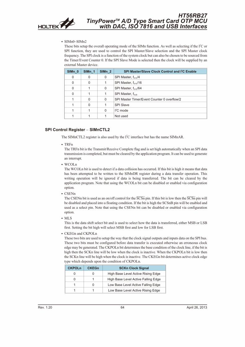
� SIMn0~SIMn2
These bits setup the overall operating mode of the SIMn function. As well as selecting if the I2C or
SPI function, they are used to control the SPI Master/Slave selection and the SPI Master clock
frequency. The SPI clock is a function of the system clock but can also be chosen to be sourced from
the Timer/Event Counter 0. If the SPI Slave Mode is selected then the clock will be supplied by an
external Master device.
SIMn_0 SIMn_1 SIMn_2 SPI Master/Slave Clock Control and I2C Enable
0 0 0 SPI Master, fSYS/4
0 0 1 SPI Master, fSYS/16
0 1 0 SPI Master, fSYS/64
0 1 1 SPI Master, fSUB
1 0 0 SPI Master Timer/Event Counter 0 overflow/2
1 0 1 SPI Slave
1 1 0 I2C mode
1 1 1 Not used
SPI Control Register � SIMnCTL2
The SIMnCTL2 register is also used by the I2C interface but has the name SIMnAR.
� TRFn
The TRFn bit is the Transmit/Receive Complete flag and is set high automatically when an SPI data
transmission is completed, but must be cleared by the application program. It can be used to generate
an interrupt.
� WCOLn
The WCOLn bit is used to detect if a data collision has occurred. If this bit is high it means that data
has been attempted to be written to the SIMnDR register during a data transfer operation. This
writing operation will be ignored if data is being transferred. The bit can be cleared by the
application program. Note that using the WCOLn bit can be disabled or enabled via configuration
option.
� CSENn
The CSENn bit is used as an on/off control for the SCSn pin. If this bit is low then the SCSn pin will
be disabled and placed into a floating condition. If the bit is high the SCSnB pin will be enabled and
used as a select pin. Note that using the CSENn bit can be disabled or enabled via configuration
option.
� MLS
This is the data shift select bit and is used to select how the data is transferred, either MSB or LSB
first. Setting the bit high will select MSB first and low for LSB first.
� CKEGn and CKPOLn
These two bits are used to setup the way that the clock signal outputs and inputs data on the SPI bus.
These two bits must be configured before data transfer is executed otherwise an erroneous clock
edge may be generated. The CKPOLn bit determines the base condition of the clock line, if the bit is
high then the SCKn line will be low when the clock is inactive. When the CKPOLn bit is low then
the SCKn line will be high when the clock is inactive. The CKEGn bit determines active clock edge
type which depends upon the condition of CKPOLn.
CKPOLn CKEGn SCKn Clock Signal
0 0 High Base Level Active Rising Edge
0 1 High Base Level Active Falling Edge
1 0 Low Base Level Active Falling Edge
1 1 Low Base Level Active Rising Edge
Rev. 1.20 64 April 26, 2013
HT56RB27TinyPowerTM A/D Type Smart Card OTP MCU
with DAC, ISO 7816 and USB Interfaces
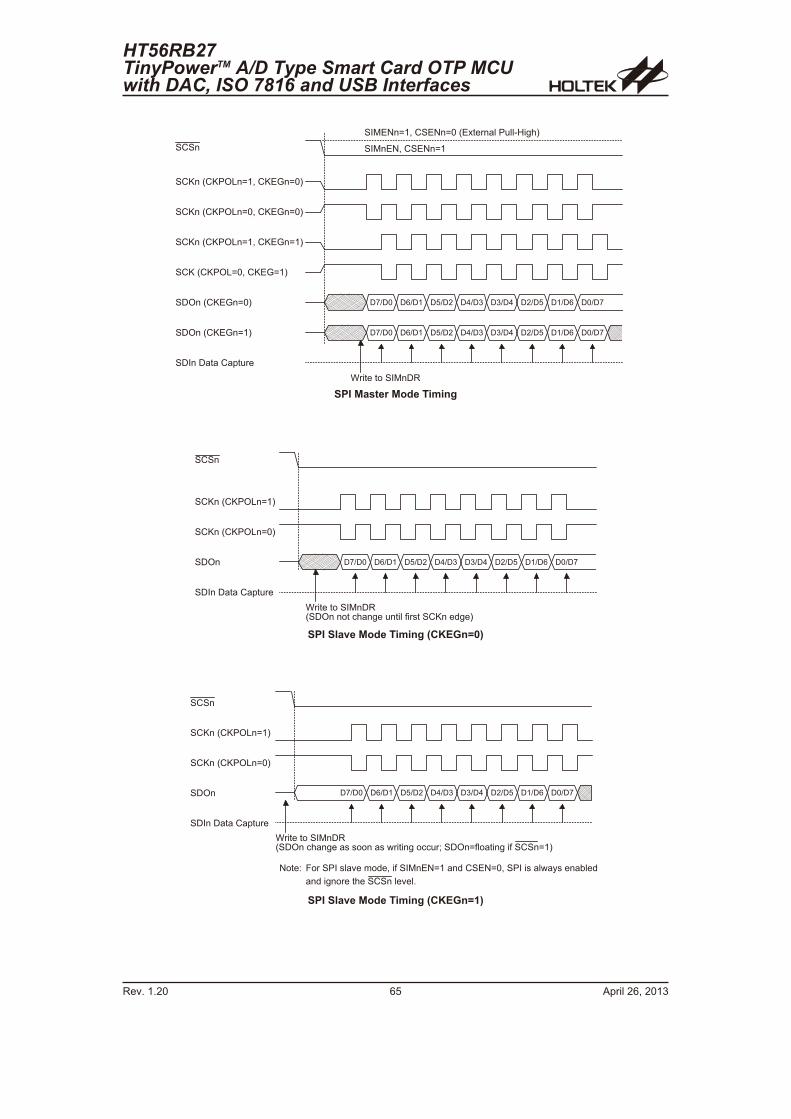
HT56RB27TinyPowerTM A/D Type Smart Card OTP MCUwith DAC, ISO 7816 and USB Interfaces
Rev. 1.20 65 April 26, 2013
# � B � � � � B � + � I � �
# � B � � � � B � + � I 7 �
# � �
# � # �
# � � � � � � � � � � � ( � � ! �
� 5 = � 7 � * = � � � ) = � � � ' = � & � & = � ' � � = � ) � � = � * � 7 = � 5
C ! � � � � � � # � / � � � # � � � � � � � � � % � � � � � � � � : � ! � � � # � B � � � ; % � �
SPI Slave Mode Timing (CKEGn=0)
# � B � � � � B � + � I � 0 � � B � @ � I 7 �
# � / � � 4 0 � � # � 4 � I �
# � / � 4 � I � 0 � � # � 4 � I 7 � � � � � � ! � � � � � � � � � 2 � % � �
# � B � � � � B � + � I 7 0 � � B � @ � I 7 �
# � B � � � � B � + � I � 0 � � B � @ � I � �
# � B � � � B � + I 7 0 � � B � @ I � �
# � � � � � B � @ � I 7 �
# � � � � � B � @ � I � �
# � # �
# � � � � � � � � � � � ( � � ! �
� 5 = � 7 � * = � � � ) = � � � ' = � & � & = � ' � � = � ) � � = � * � 7 = � 5
� 5 = � 7 � * = � � � ) = � � � ' = � & � & = � ' � � = � ) � � = � * � 7 = � 5
C ! � � � � � � # � / � �
SPI Master Mode Timing
# � B � � � � B � + � I � �
# � B � � � � B � + � I 7 �
# � �
# � # �
# � � � � � � � � � � � ( � � ! �
� 5 = � 7 � * = � � � ) = � � � ' = � & � & = � ' � � = � ) � � = � * � 7 = � 5
C ! � � � � � � # � / � � � # � � � � � � % � � � � � � � � � � � ? ! � � � � % � � ! K � # � � I : � � � � � % � � : � # � # � I � �
4 � � . � ! � # � � � � � � 9 � � � ; � 0 � � : � # � / � � 4 I � � � � ; � � # � 4 I 7 0 � # � � � � � � � � ? � $ � � � � � < � � ;
� � ; � � % � ! � � � � � � # � # � � � � 9 � � �
SPI Slave Mode Timing (CKEGn=1)
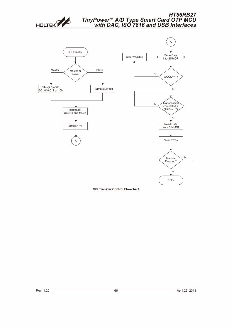
Rev. 1.20 66 April 26, 2013
HT56RB27TinyPowerTM A/D Type Smart Card OTP MCU
with DAC, ISO 7816 and USB Interfaces
# � / � � 4 � I �
C ! � � � � � � � �� � � � # � / � �
C � + � I � L
� � � � ! � C � + �
-
� ! � � � � � � � � � � ( � � � � ; � L� � � � I � � L � �
4
-
� � ; � � � � �: ! � � # � / � �
� � � � ! � � � �
� ! � � � : � !� � � � � � � ; L
4
-
� 4 �
� � � � � ! � !� � � 9 �
/ � � � � ! # � � 9 �
,
,
# � � � � ! � � � : � ! �
� : � % � ! �� # � 4 � � � � ; � / + # � �
# � / � 1 � . 7 3 I 7 7 7 07 7 � 0 7 � 7 0 7 � � � ! � � 7 7 �
# � / � 1 � . 7 3 I � 7 � 4
SPI Transfer Control Flowchart
SPI Communication
After the SPI interface is enabled by setting the SIMnEN bit high, then in the Master Mode, when data
is written to the SIMnDR register, transmission/reception will begin simultaneously. When the data
transfer is complete, the TRFn flag will be set automatically, but must be cleared using the application
program. In the Slave Mode, when the clock signal from the master has been received, any data in the
SIMnDR register will be transmitted and any data on the SDIn pin will be shifted into the SIMnDR
register. The master should output a SCSn signal to enable the slave device before a clock signal is
provided and slave data transfers should be enabled/disabled before/after an SCSn signal is received.
The SPI will continue to function even after a HALT instruction has been executed.
I2C Interface
The I2C interface is used to communicate with external peripheral devices such as sensors, EEPROM
memory etc. Originally developed by Philips, it is a two line low speed serial interface for synchronous
serial data transfer. The advantage of only two lines for communication, relatively simple
communication protocol and the ability to accommodate multiple devices on the same bus has made it
an extremely popular interface type for many applications.
I2C Interface Operation
The I2C serial interface is a two line interface, a serial data line, , and serial clock line, SCLn. As many
devices may be connected together on the same bus, their outputs are both open drain types. For this
reason it is necessary that external pull-high resistors are connected to these outputs. Note that no chip
select line exists, as each device on the I2C bus is identified by a unique address which will be
transmitted and received on the I2C bus.
When two devices communicate with each other on the bidirectional I2C bus, one is known as the
master device and one as the slave device. Both master and slave can transmit and receive data,
however, it is the master device that has overall control of the bus. For these devices, which only
operates in slave mode, there are two methods of transferring data on the I2C bus, the slave transmit
mode and the slave receive mode.
There are several configuration options associated with the I2C interface. One of these is to enable the
function which selects the SIMn pins rather than normal I/O pins. Note that if the configuration option
does not select the SIMn function then the SIMnEN bit in the SIMnCTL0 register will have no effect.
A configuration option exists to allow a clock other than the system clock to drive the I2C interface.
Another configuration option determines the debounce time of the I2C interface. This uses the internal
clock to in effect add a debounce time to the external clock to reduce the possibility of glitches on the
clock line causing erroneous operation. The debounce time, if selected, can be chosen to be either 1 or
2 system clocks.
Configuration Option Function
SIMn function SIMn interface or I/O pins
I2C debounce No debounce, 1 system clock; 2 system clocks
I2C Interface Configuration Options
HT56RB27TinyPowerTM A/D Type Smart Card OTP MCUwith DAC, ISO 7816 and USB Interfaces
Rev. 1.20 67 April 26, 2013
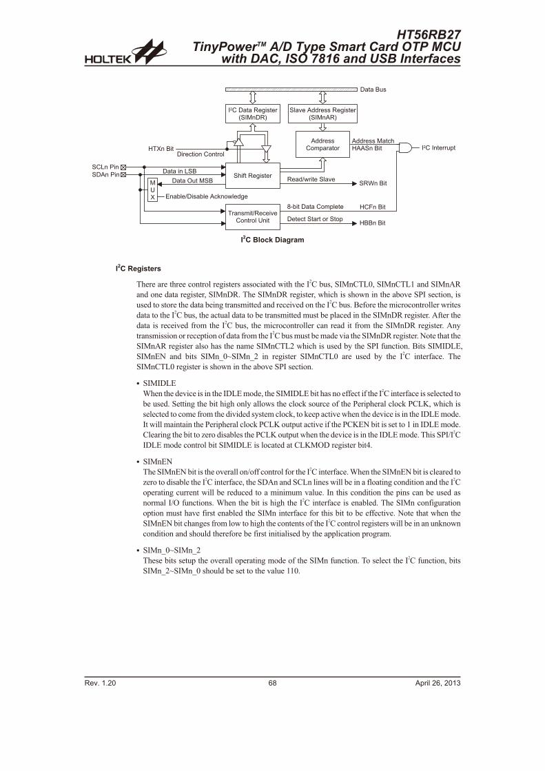
I2C Registers
There are three control registers associated with the I2C bus, SIMnCTL0, SIMnCTL1 and SIMnAR
and one data register, SIMnDR. The SIMnDR register, which is shown in the above SPI section, is
used to store the data being transmitted and received on the I2C bus. Before the microcontroller writes
data to the I2C bus, the actual data to be transmitted must be placed in the SIMnDR register. After the
data is received from the I2C bus, the microcontroller can read it from the SIMnDR register. Any
transmission or reception of data from the I2C bus must be made via the SIMnDR register. Note that the
SIMnAR register also has the name SIMnCTL2 which is used by the SPI function. Bits SIMIDLE,
SIMnEN and bits SIMn_0~SIMn_2 in register SIMnCTL0 are used by the I2C interface. The
SIMnCTL0 register is shown in the above SPI section.
� SIMIDLE
When the device is in the IDLE mode, the SIMIDLE bit has no effect if the I2C interface is selected to
be used. Setting the bit high only allows the clock source of the Peripheral clock PCLK, which is
selected to come from the divided system clock, to keep active when the device is in the IDLE mode.
It will maintain the Peripheral clock PCLK output active if the PCKEN bit is set to 1 in IDLE mode.
Clearing the bit to zero disables the PCLK output when the device is in the IDLE mode. This SPI/I2C
IDLE mode control bit SIMIDLE is located at CLKMOD register bit4.
� SIMnEN
The SIMnEN bit is the overall on/off control for the I2C interface. When the SIMnEN bit is cleared to
zero to disable the I2C interface, the SDAn and SCLn lines will be in a floating condition and the I
2C
operating current will be reduced to a minimum value. In this condition the pins can be used as
normal I/O functions. When the bit is high the I2C interface is enabled. The SIMn configuration
option must have first enabled the SIMn interface for this bit to be effective. Note that when the
SIMnEN bit changes from low to high the contents of the I2C control registers will be in an unknown
condition and should therefore be first initialised by the application program.
� SIMn_0~SIMn_2
These bits setup the overall operating mode of the SIMn function. To select the I2C function, bits
SIMn_2~SIMn_0 should be set to the value 110.
Rev. 1.20 68 April 26, 2013
HT56RB27TinyPowerTM A/D Type Smart Card OTP MCU
with DAC, ISO 7816 and USB Interfaces
� � � � � � � � � � % � � � � !� # � / � � �
# � � 9 � � , ; ; ! � � � � � % � � � � !� # � / � , �
# � � : � � � % � � � � !
� � ! � � � � � � � � ! �
/>D
, ; ; ! � � � � / � � �2 , , # � � 8 � � � � � � � � � � ! ! � ( �
� � � � � � � � + # 8
� � � � � � � � / # 8
� ! � � � � � � = � � � 9 �� � � ! � � > � � �
6 � < � � � � � � � � � � ( � � � �
� � � � � � # � � ! � � ! � # � (
� � � � � 8 � �
, ; ; ! � � �� � ( � ! � � !
� � � < � � = � � � � < � � � , " � ? � � ; % �
� � ; = ? ! � � � � # � � 9 �# C � � 8 � �
2 8 8 � � 8 � �
2 � D � � 8 � �
# � + � � � � �
# � , � � � � �
2 � � � � 8 � �
I2C Block Diagram
� RXAKn
The RXAKn flag is the reception acknowledge flag. When the RXAKn bit has been reset to zero, it
means that a correct acknowledge signal has been received at the 9th clock, after 8 bits of data have
been transmitted. When in the transmit mode, the transmitter checks the RXAKn bit to determine if
the receiver wishes to receive the next byte. The transmitter will therefore continue sending out data
until the RXAKn bit is set high. When this occurs, the transmitter will release the SDAn line to allow
the master to send a STOP signal to release the bus.
� SRWn
The SRWn bit is the Slave Read/Write bit. This bit determines whether the master device wishes to
transmit or receive data from the I2C bus. When the transmitted address and slave address match,
which is when the HAASn bit is set high, the device will check the SRWn bit to determine whether it
should be in transmit mode or receive mode. If the SRWn bit is high, the master is requesting to read
data from the bus, so the device should be in transmit mode. When the SRWn bit is zero, the master
will write data to the bus, therefore the device should be in receive mode to read this data.
� TXAKn
The TXAKn flag is the transmission acknowledge flag. After the receipt of 8-bits of data, this bit will
be transmitted to the bus on the 9th clock. To continue receiving more data, this bit has to be reset to
zero before further data is received.
� HTXn
The HTXn flag is the transmit/receive mode bit. This flag should be set high to set the transmit mode
and low for the receive mode.
� HBBn
The HBBn flag is the I2C busy flag. This flag will be high when the I
2C bus is busy which will occur
when a START signal is detected. The flag will be reset to zero when the bus is free which will occur
when a STOP signal is detected.
� HAASn
The HAASn flag is the address match flag. This flag is used to determine if the slave device address
is the same as the master transmit address. If the addresses match then this bit will be high, if there is
no match then the flag will be low.
� HCFn
The HCFn flag is the data transfer flag. This flag will be zero when data is being transferred. Upon
completion of an 8-bit data transfer the flag will go high and an interrupt will be generated.
I2C Control Register � SIMAR
The SIMnAR register is also used by the SPI interface but has the name SIMnCTL2. The SIMnAR
register is the location where the 7-bit slave address of the microcontroller is stored. Bits 1~7 of the
SIMnAR register define the microcontroller slave address. Bit 0 is not defined. When a master device,
which is connected to the I2C bus, sends out an address, which matches the slave address in the
SIMnAR register, the microcontroller slave device will be selected. Note that the SIMnAR register is
the same register as SIMnCTL2 which is used by the SPI interface.
HT56RB27TinyPowerTM A/D Type Smart Card OTP MCUwith DAC, ISO 7816 and USB Interfaces
Rev. 1.20 69 April 26, 2013
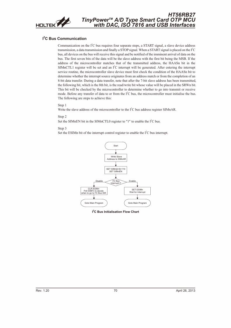
I2C Bus Communication
Communication on the I2C bus requires four separate steps, a START signal, a slave device address
transmission, a data transmission and finally a STOP signal. When a START signal is placed on the I2C
bus, all devices on the bus will receive this signal and be notified of the imminent arrival of data on the
bus. The first seven bits of the data will be the slave address with the first bit being the MSB. If the
address of the microcontroller matches that of the transmitted address, the HAASn bit in the
SIMnCTL1 register will be set and an I2C interrupt will be generated. After entering the interrupt
service routine, the microcontroller slave device must first check the condition of the HAASn bit to
determine whether the interrupt source originates from an address match or from the completion of an
8-bit data transfer. During a data transfer, note that after the 7-bit slave address has been transmitted,
the following bit, which is the 8th bit, is the read/write bit whose value will be placed in the SRWn bit.
This bit will be checked by the microcontroller to determine whether to go into transmit or receive
mode. Before any transfer of data to or from the I2C bus, the microcontroller must initialise the bus.
The following are steps to achieve this:
Step 1
Write the slave address of the microcontroller to the I2C bus address register SIMnAR.
Step 2
Set the SIMnEN bit in the SIMnCTL0 register to �1� to enable the I2C bus.
Step 3
Set the ESIMn bit of the interrupt control register to enable the I2C bus interrupt.
Rev. 1.20 70 April 26, 2013
HT56RB27TinyPowerTM A/D Type Smart Card OTP MCU
with DAC, ISO 7816 and USB Interfaces
# � � ! �
� � C ! � � � � # � � 9 �� � , ; ; ! � � � � � � # � / � ,
# � � � # � / � 1 � . 7 3 I � � 7# � � � # � / � � 4
� � � � � � � 8 � �� � � � ! ! � ( � I L
�
� � � < � �� � � � < � �
# � � � � # � / �C � � � � : ! � � � � � ! ! � ( �
@ � � / � � � � � ! % ! � �
� + � � # � / � �� � � � # � / � � � � � ; � � ; � �
? � � � � � � % � � � � � � � 8 � � � � # �
@ � � / � � � � � ! % ! � �
I2C Bus Initialisation Flow Chart
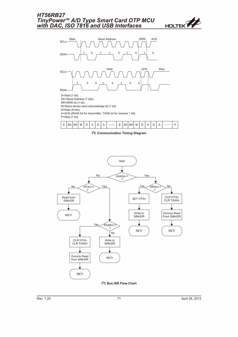
HT56RB27TinyPowerTM A/D Type Smart Card OTP MCUwith DAC, ISO 7816 and USB Interfaces
Rev. 1.20 71 April 26, 2013
� � � �
� 7 � � � � � � � �7 7 � � � � � � � � 77
� 7 7 � 7 � 7� �
# I # � � ! � � � � � < � � �
# , I # � � 9 � � , ; ; ! � � � � � 5 � < � � � �
# I # C � < � � � � � � < � � �
/ I # � � 9 � � ; � 9 � � � � � � ; � � " � ? � � ; % � � < � � � � � � < � � �
� I � � � � � � 6 � < � � � �
, I , � B � � D , B � < � � � : ! � � ! � � � � � � � � ! 0 � � D , B � < � � � : ! � ! � � � 9 � ! � � � < � � �
� I # � ( � � � � < � � �
# � + �# � � ! �
# � , �
# C , � B
, � B # � (# � + �
# � , �
# � � 9 � � , ; ; ! � � �
# # , # / � , � , # # , # / � , � , �
I2C Communication Timing Diagram
# � � ! �
2 , , # � I �L
2 � D � I �� � � � L
# C � I �� � � � � L
- � �4
- � � 4
D , B � I �L
- � �
4
4
� � ; � : ! �# � / � �
� � �
- � �
� � � � $ � � � ;: ! � � # � / � �
� � �
� � �
C ! � � � � � # � / � �
# � � � 2 � D �
C ! � � � � � # � / � �
� � � � $ � � � ;� ! � � # � / � �
� + � 2 � D �� + � � D , B �
� � � � � �
� + � 2 � D �� + � � D , B �
I2C Bus ISR Flow Chart
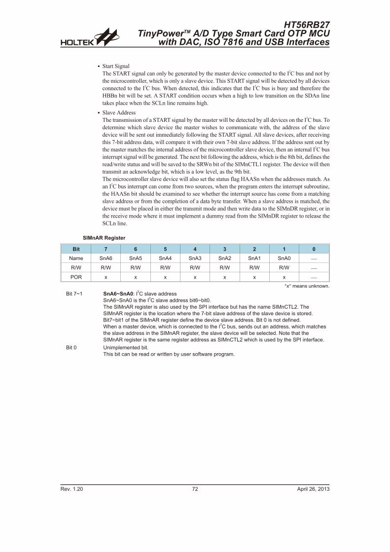
� Start Signal
The START signal can only be generated by the master device connected to the I2C bus and not by
the microcontroller, which is only a slave device. This START signal will be detected by all devices
connected to the I2C bus. When detected, this indicates that the I
2C bus is busy and therefore the
HBBn bit will be set. A START condition occurs when a high to low transition on the SDAn line
takes place when the SCLn line remains high.
� Slave Address
The transmission of a START signal by the master will be detected by all devices on the I2C bus. To
determine which slave device the master wishes to communicate with, the address of the slave
device will be sent out immediately following the START signal. All slave devices, after receiving
this 7-bit address data, will compare it with their own 7-bit slave address. If the address sent out by
the master matches the internal address of the microcontroller slave device, then an internal I2C bus
interrupt signal will be generated. The next bit following the address, which is the 8th bit, defines the
read/write status and will be saved to the SRWn bit of the SIMnCTL1 register. The device will then
transmit an acknowledge bit, which is a low level, as the 9th bit.
The microcontroller slave device will also set the status flag HAASn when the addresses match. As
an I2C bus interrupt can come from two sources, when the program enters the interrupt subroutine,
the HAASn bit should be examined to see whether the interrupt source has come from a matching
slave address or from the completion of a data byte transfer. When a slave address is matched, the
device must be placed in either the transmit mode and then write data to the SIMnDR register, or in
the receive mode where it must implement a dummy read from the SIMnDR register to release the
SCLn line.
SIMnAR Register
Bit 7 6 5 4 3 2 1 0
Name SnA6 SnA5 SnA4 SnA3 SnA2 SnA1 SnA0 �
R/W R/W R/W R/W R/W R/W R/W R/W �
POR x x x x x x x �
�x� means unknown.
Bit 7~1 SnA6~SnA0: I2C slave address
SnA6~SnA0 is the I2C slave address bit6~bit0.
The SIMnAR register is also used by the SPI interface but has the name SIMnCTL2. The
SIMnAR register is the location where the 7-bit slave address of the slave device is stored.
Bit7~bit1 of the SIMnAR register define the device slave address. Bit 0 is not defined.
When a master device, which is connected to the I2C bus, sends out an address, which matches
the slave address in the SIMnAR register, the slave device will be selected. Note that the
SIMnAR register is the same register address as SIMnCTL2 which is used by the SPI interface.
Bit 0 Unimplemented bit.
This bit can be read or written by user software program.
Rev. 1.20 72 April 26, 2013
HT56RB27TinyPowerTM A/D Type Smart Card OTP MCU
with DAC, ISO 7816 and USB Interfaces
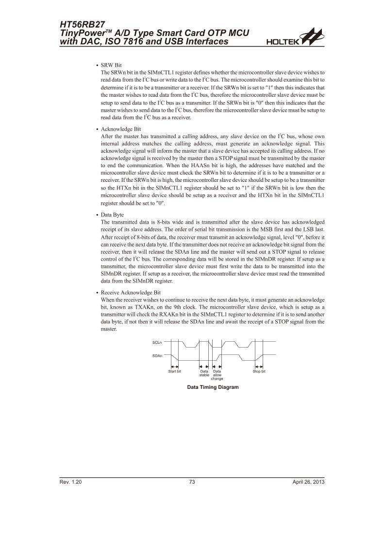
� SRW Bit
The SRWn bit in the SIMnCTL1 register defines whether the microcontroller slave device wishes to
read data from the I2C bus or write data to the I
2C bus. The microcontroller should examine this bit to
determine if it is to be a transmitter or a receiver. If the SRWn bit is set to �1� then this indicates that
the master wishes to read data from the I2C bus, therefore the microcontroller slave device must be
setup to send data to the I2C bus as a transmitter. If the SRWn bit is �0� then this indicates that the
master wishes to send data to the I2C bus, therefore the microcontroller slave device must be setup to
read data from the I2C bus as a receiver.
� Acknowledge Bit
After the master has transmitted a calling address, any slave device on the I2C bus, whose own
internal address matches the calling address, must generate an acknowledge signal. This
acknowledge signal will inform the master that a slave device has accepted its calling address. If no
acknowledge signal is received by the master then a STOP signal must be transmitted by the master
to end the communication. When the HAASn bit is high, the addresses have matched and the
microcontroller slave device must check the SRWn bit to determine if it is to be a transmitter or a
receiver. If the SRWn bit is high, the microcontroller slave device should be setup to be a transmitter
so the HTXn bit in the SIMnCTL1 register should be set to �1� if the SRWn bit is low then the
microcontroller slave device should be setup as a receiver and the HTXn bit in the SIMnCTL1
register should be set to �0�.
� Data Byte
The transmitted data is 8-bits wide and is transmitted after the slave device has acknowledged
receipt of its slave address. The order of serial bit transmission is the MSB first and the LSB last.
After receipt of 8-bits of data, the receiver must transmit an acknowledge signal, level �0�, before it
can receive the next data byte. If the transmitter does not receive an acknowledge bit signal from the
receiver, then it will release the SDAn line and the master will send out a STOP signal to release
control of the I2C bus. The corresponding data will be stored in the SIMnDR register. If setup as a
transmitter, the microcontroller slave device must first write the data to be transmitted into the
SIMnDR register. If setup as a receiver, the microcontroller slave device must read the transmitted
data from the SIMnDR register.
� Receive Acknowledge Bit
When the receiver wishes to continue to receive the next data byte, it must generate an acknowledge
bit, known as TXAKn, on the 9th clock. The microcontroller slave device, which is setup as a
transmitter will check the RXAKn bit in the SIMnCTL1 register to determine if it is to send another
data byte, if not then it will release the SDAn line and await the receipt of a STOP signal from the
master.
HT56RB27TinyPowerTM A/D Type Smart Card OTP MCUwith DAC, ISO 7816 and USB Interfaces
Rev. 1.20 73 April 26, 2013
# � + �
# � , �
# � � ! � � < � � � � � � � �� � � � < � �
� � � � � �� � � � � ? � � � % �
# � ( � < � �
Data Timing Diagram
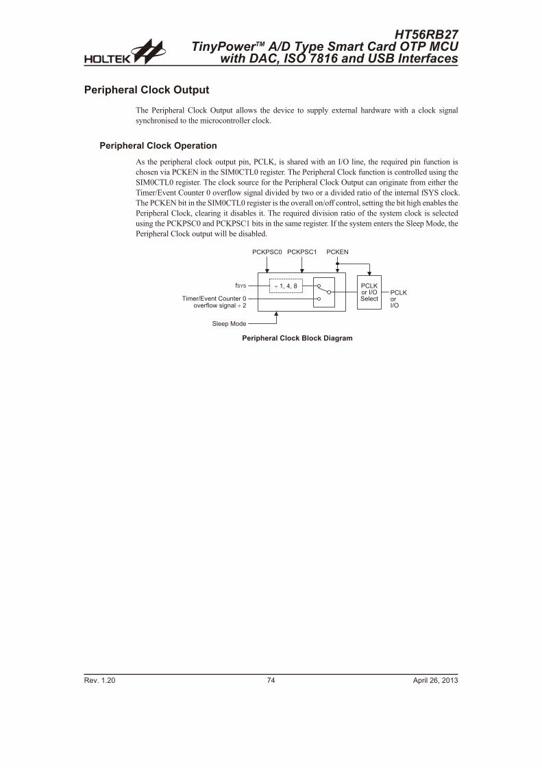
Peripheral Clock Output
The Peripheral Clock Output allows the device to supply external hardware with a clock signal
synchronised to the microcontroller clock.
Peripheral Clock Operation
As the peripheral clock output pin, PCLK, is shared with an I/O line, the required pin function is
chosen via PCKEN in the SIM0CTL0 register. The Peripheral Clock function is controlled using the
SIM0CTL0 register. The clock source for the Peripheral Clock Output can originate from either the
Timer/Event Counter 0 overflow signal divided by two or a divided ratio of the internal fSYS clock.
The PCKEN bit in the SIM0CTL0 register is the overall on/off control, setting the bit high enables the
Peripheral Clock, clearing it disables it. The required division ratio of the system clock is selected
using the PCKPSC0 and PCKPSC1 bits in the same register. If the system enters the Sleep Mode, the
Peripheral Clock output will be disabled.
Rev. 1.20 74 April 26, 2013
HT56RB27TinyPowerTM A/D Type Smart Card OTP MCU
with DAC, ISO 7816 and USB Interfaces
: # - #
� � � � ! = � 9 � � � � � � � � � ! � 7 9 � ! : � ? � � � % � � � � � � �
� � + B ! � � = # � � � �
� � + B !� =
� � � 0 � ' 0 � 6
� � B � 4� � B � # � 7 � � B � # � �
# � � � ( � / ; �
Peripheral Clock Block Diagram
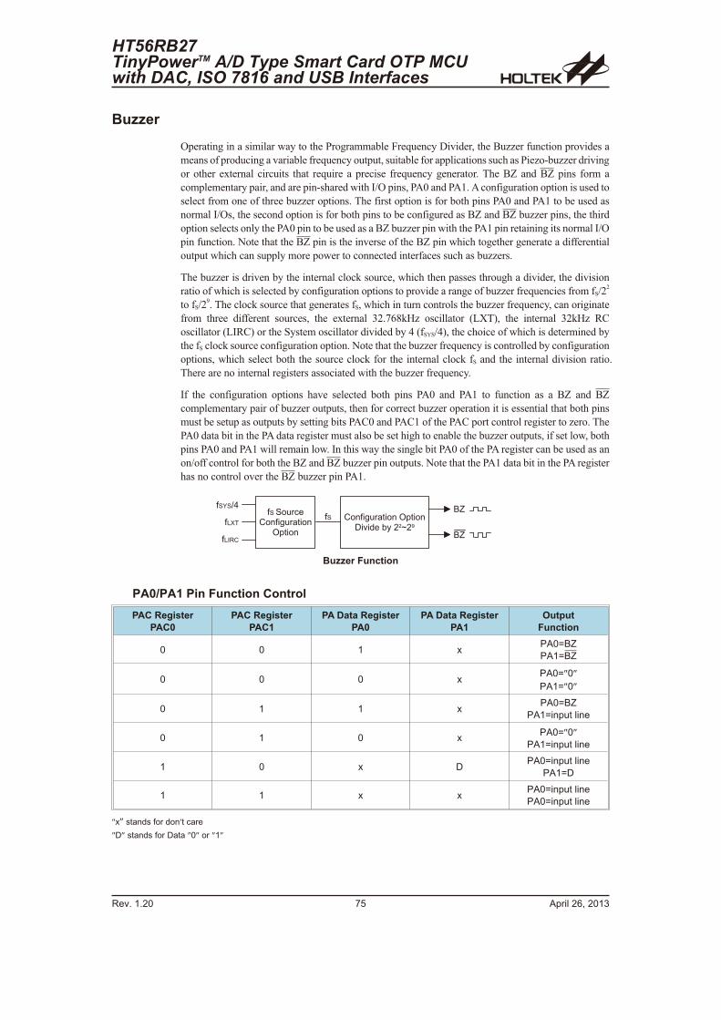
Buzzer
Operating in a similar way to the Programmable Frequency Divider, the Buzzer function provides a
means of producing a variable frequency output, suitable for applications such as Piezo-buzzer driving
or other external circuits that require a precise frequency generator. The BZ and BZ pins form a
complementary pair, and are pin-shared with I/O pins, PA0 and PA1. A configuration option is used to
select from one of three buzzer options. The first option is for both pins PA0 and PA1 to be used as
normal I/Os, the second option is for both pins to be configured as BZ and BZ buzzer pins, the third
option selects only the PA0 pin to be used as a BZ buzzer pin with the PA1 pin retaining its normal I/O
pin function. Note that the BZ pin is the inverse of the BZ pin which together generate a differential
output which can supply more power to connected interfaces such as buzzers.
The buzzer is driven by the internal clock source, which then passes through a divider, the division
ratio of which is selected by configuration options to provide a range of buzzer frequencies from fS/22
to fS/29. The clock source that generates fS, which in turn controls the buzzer frequency, can originate
from three different sources, the external 32.768kHz oscillator (LXT), the internal 32kHz RC
oscillator (LIRC) or the System oscillator divided by 4 (fSYS/4), the choice of which is determined by
the fS clock source configuration option. Note that the buzzer frequency is controlled by configuration
options, which select both the source clock for the internal clock fS and the internal division ratio.
There are no internal registers associated with the buzzer frequency.
If the configuration options have selected both pins PA0 and PA1 to function as a BZ and BZ
complementary pair of buzzer outputs, then for correct buzzer operation it is essential that both pins
must be setup as outputs by setting bits PAC0 and PAC1 of the PAC port control register to zero. The
PA0 data bit in the PA data register must also be set high to enable the buzzer outputs, if set low, both
pins PA0 and PA1 will remain low. In this way the single bit PA0 of the PA register can be used as an
on/off control for both the BZ and BZ buzzer pin outputs. Note that the PA1 data bit in the PA register
has no control over the BZ buzzer pin PA1.
PA0/PA1 Pin Function Control
PAC Register
PAC0
PAC Register
PAC1
PA Data Register
PA0
PA Data Register
PA1
Output
Function
0 0 1 xPA0=BZ
PA1=BZ
0 0 0 xPA0=�0�
PA1=�0�
0 1 1 xPA0=BZ
PA1=input line
0 1 0 xPA0=�0�
PA1=input line
1 0 x DPA0=input line
PA1=D
1 1 x xPA0=input line
PA0=input line
�x� stands for don�t care
�D� stands for Data �0� or �1�
HT56RB27TinyPowerTM A/D Type Smart Card OTP MCUwith DAC, ISO 7816 and USB Interfaces
Rev. 1.20 75 April 26, 2013
: # � # � ! �� � : � % � ! � � � �
( � � �
: # - # = '
: + D �
: + � �
� � : � % � ! � � � � � ( � � �� � 9 � ; � � < $ � � � G � A
: #8 M
8 M
Buzzer Function
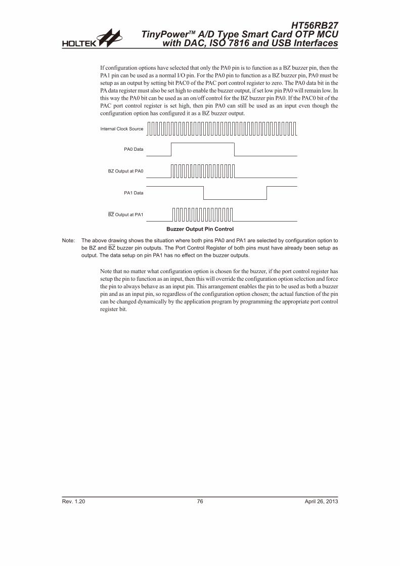
If configuration options have selected that only the PA0 pin is to function as a BZ buzzer pin, then the
PA1 pin can be used as a normal I/O pin. For the PA0 pin to function as a BZ buzzer pin, PA0 must be
setup as an output by setting bit PAC0 of the PAC port control register to zero. The PA0 data bit in the
PAdata register must also be set high to enable the buzzer output, if set low pin PA0 will remain low. In
this way the PA0 bit can be used as an on/off control for the BZ buzzer pin PA0. If the PAC0 bit of the
PAC port control register is set high, then pin PA0 can still be used as an input even though the
configuration option has configured it as a BZ buzzer output.
Note that no matter what configuration option is chosen for the buzzer, if the port control register has
setup the pin to function as an input, then this will override the configuration option selection and force
the pin to always behave as an input pin. This arrangement enables the pin to be used as both a buzzer
pin and as an input pin, so regardless of the configuration option chosen; the actual function of the pin
can be changed dynamically by the application program by programming the appropriate port control
register bit.
Rev. 1.20 76 April 26, 2013
HT56RB27TinyPowerTM A/D Type Smart Card OTP MCU
with DAC, ISO 7816 and USB Interfaces
� � � � ! � � � � � � " � # � ! �
� , 7 � � � � �
8 M � � � ( � � � � � � � , 7
8 M � � � ( � � � � � � � , �
� , � � � � � �
Buzzer Output Pin Control
Note: The above drawing shows the situation where both pins PA0 and PA1 are selected by configuration option to
be BZ and BZ buzzer pin outputs. The Port Control Register of both pins must have already been setup as
output. The data setup on pin PA1 has no effect on the buzzer outputs.
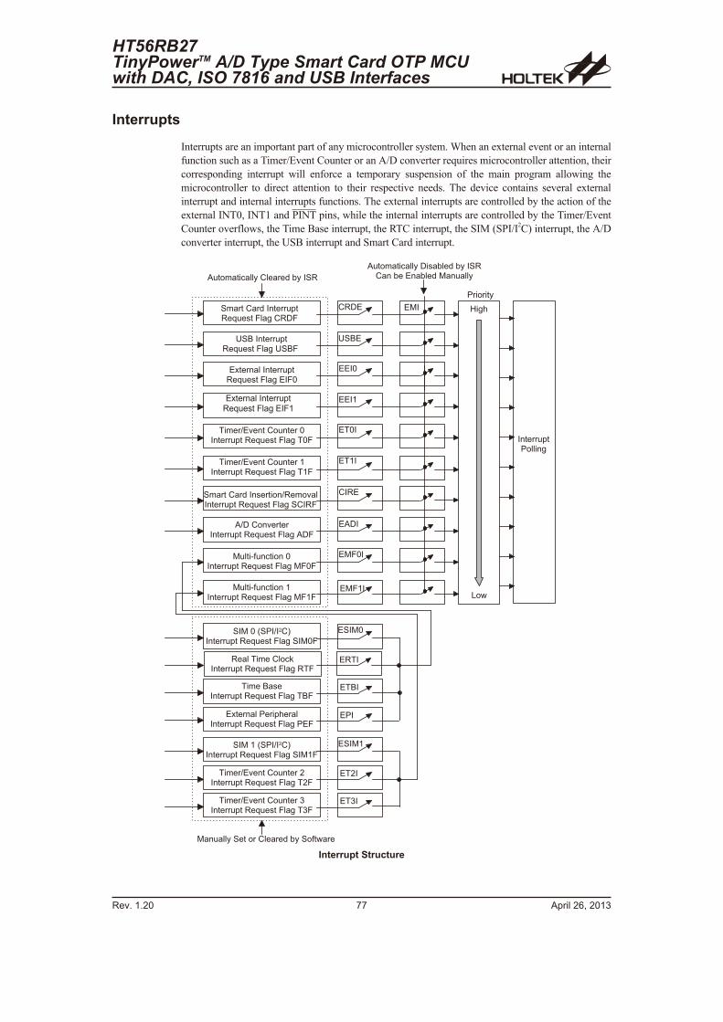
Interrupts
Interrupts are an important part of any microcontroller system. When an external event or an internal
function such as a Timer/Event Counter or an A/D converter requires microcontroller attention, their
corresponding interrupt will enforce a temporary suspension of the main program allowing the
microcontroller to direct attention to their respective needs. The device contains several external
interrupt and internal interrupts functions. The external interrupts are controlled by the action of the
external INT0, INT1 and PINT pins, while the internal interrupts are controlled by the Timer/Event
Counter overflows, the Time Base interrupt, the RTC interrupt, the SIM (SPI/I2C) interrupt, the A/D
converter interrupt, the USB interrupt and Smart Card interrupt.
HT56RB27TinyPowerTM A/D Type Smart Card OTP MCUwith DAC, ISO 7816 and USB Interfaces
Rev. 1.20 77 April 26, 2013
, � � � � � � � � � $ � � � � � ! � ; � < $ � � #
, � � � � � � � � � $ � � � � � < � � ; � < $ � � # � � � � < � � � � � < � � ; � / � � � � � � $
� ! � ! � � $
2 � % �
� � � � ! ! � ( �� � � � � %
� � � � ! � � � � � � � � ! ! � ( � � N � � � � � � � � % � � � � �
� � � 7
� � � � ! = � 9 � � � � � � � � � ! � 7� � � � ! ! � ( � � � N � � � � � � � � % � � 7 �
� � � �
� � 7 �
� � � � ! = � 9 � � � � � � � � � ! � �� � � � ! ! � ( � � � N � � � � � � � � % � � � �
� � � �
� � � � ! � � � � � � � � ! ! � ( � � N � � � � � � � � % � � � � 7
� / �
+ ?
� � � � � 8 � � �� � � � ! ! � ( � � � N � � � � � � � � % � � 8 �
� , � �
� � � � � � � � � � � "� � � � ! ! � ( � � � N � � � � � � � � % � � �
� � �
, = � � � � 9 � ! � � !� � � � ! ! � ( � � � N � � � � � � � � % � , � �
� � 8 �
� � � � ! = � 9 � � � � � � � � � ! � �� � � � ! ! � ( � � � N � � � � � � � � % � � � �
� � � �
� � � � ! = � 9 � � � � � � � � � ! � &� � � � ! ! � ( � � � N � � � � � � � � % � � & �
� � & �
/ � � � � � � $ � # � � � ! � � � � � ! � ; � < $ � # : � ? � ! �
� � �� � � � ! � � � � � � ! � ( � � ! � �� � � � ! ! � ( � � � N � � � � � � � � % � � � �
� # � / 7
/ � � � � � : � � � � � � �� � � � ! ! � ( � � � N � � � � � � � � % � / � � �
� / � � �
# � / � 7 � � # � � = � � � �� � � � ! ! � ( � � � N � � � � � � � � % � # � / 7 �
/ � � � � � : � � � � � � 7� � � � ! ! � ( � � � N � � � � � � � � % � / � 7 �
# � / � � � � # � � = � � � �� � � � ! ! � ( � � � N � � � � � � � � % � # � / � �
� / � 7 �
� # � / �
# � � ! � � � � ! ; � � � � � ! ! � ( � � N � � � � � � � � % � � � �
� � �
� � �# � � ! � � � � ! ; � � � � � ! � � � = � � 9 � �� � � � ! ! � ( � � � N � � � � � � � � % � # � � �
� > # 8 � � � � � ! ! � ( � � N � � � � � � � � % � > # 8 �
> # 8 �
Interrupt Structure
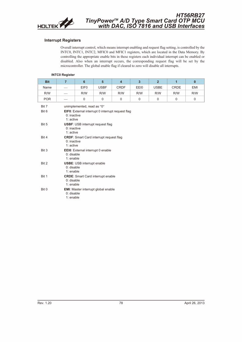
Interrupt Registers
Overall interrupt control, which means interrupt enabling and request flag setting, is controlled by the
INTC0, INTC1, INTC2, MFIC0 and MFIC1 registers, which are located in the Data Memory. By
controlling the appropriate enable bits in these registers each individual interrupt can be enabled or
disabled. Also when an interrupt occurs, the corresponding request flag will be set by the
microcontroller. The global enable flag if cleared to zero will disable all interrupts.
INTC0 Register
Bit 7 6 5 4 3 2 1 0
Name � EIF0 USBF CRDF EEI0 USBE CRDE EMI
R/W � R/W R/W R/W R/W R/W R/W R/W
POR � 0 0 0 0 0 0 0
Bit 7 unimplemented, read as �0�
Bit 6 EIF0: External interrupt 0 interrupt request flag
0: inactive
1: active
Bit 5 USBF: USB interrupt request flag
0: inactive
1: active
Bit 4 CRDF: Smart Card interrupt request flag
0: inactive
1: active
Bit 3 EEI0: External interrupt 0 enable
0: disable
1: enable
Bit 2 USBE: USB interrupt enable
0: disable
1: enable
Bit 1 CRDE: Smart Card interrupt enable
0: disable
1: enable
Bit 0 EMI: Master interrupt global enable
0: disable
1: enable
Rev. 1.20 78 April 26, 2013
HT56RB27TinyPowerTM A/D Type Smart Card OTP MCU
with DAC, ISO 7816 and USB Interfaces
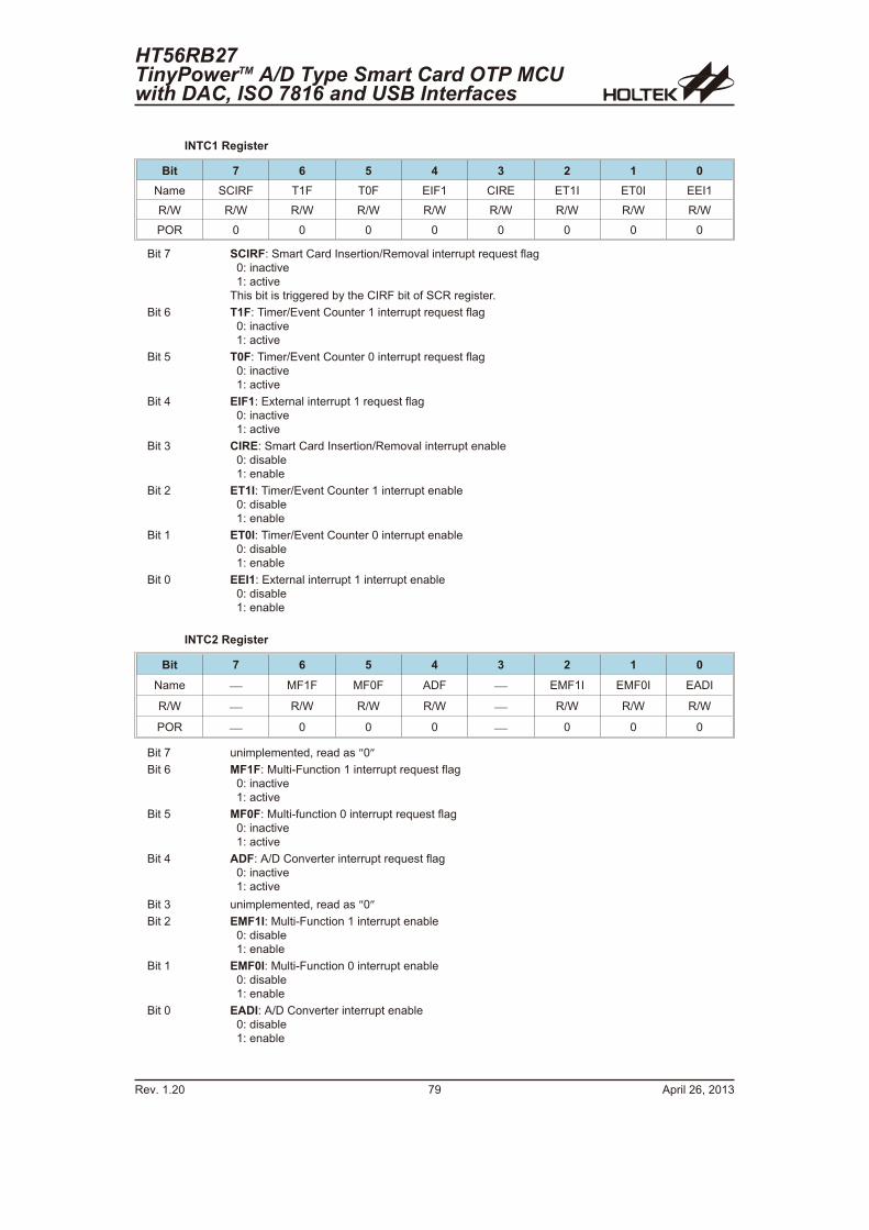
INTC1 Register
Bit 7 6 5 4 3 2 1 0
Name SCIRF T1F T0F EIF1 CIRE ET1I ET0I EEI1
R/W R/W R/W R/W R/W R/W R/W R/W R/W
POR 0 0 0 0 0 0 0 0
Bit 7 SCIRF: Smart Card Insertion/Removal interrupt request flag0: inactive1: active
This bit is triggered by the CIRF bit of SCR register.
Bit 6 T1F: Timer/Event Counter 1 interrupt request flag0: inactive1: active
Bit 5 T0F: Timer/Event Counter 0 interrupt request flag0: inactive1: active
Bit 4 EIF1: External interrupt 1 request flag0: inactive1: active
Bit 3 CIRE: Smart Card Insertion/Removal interrupt enable0: disable1: enable
Bit 2 ET1I: Timer/Event Counter 1 interrupt enable0: disable1: enable
Bit 1 ET0I: Timer/Event Counter 0 interrupt enable0: disable1: enable
Bit 0 EEI1: External interrupt 1 interrupt enable0: disable1: enable
INTC2 Register
Bit 7 6 5 4 3 2 1 0
Name � MF1F MF0F ADF � EMF1I EMF0I EADI
R/W � R/W R/W R/W � R/W R/W R/W
POR � 0 0 0 � 0 0 0
Bit 7 unimplemented, read as �0�
Bit 6 MF1F: Multi-Function 1 interrupt request flag0: inactive1: active
Bit 5 MF0F: Multi-function 0 interrupt request flag0: inactive1: active
Bit 4 ADF: A/D Converter interrupt request flag0: inactive1: active
Bit 3 unimplemented, read as �0�
Bit 2 EMF1I: Multi-Function 1 interrupt enable0: disable1: enable
Bit 1 EMF0I: Multi-Function 0 interrupt enable0: disable1: enable
Bit 0 EADI: A/D Converter interrupt enable0: disable1: enable
HT56RB27TinyPowerTM A/D Type Smart Card OTP MCUwith DAC, ISO 7816 and USB Interfaces
Rev. 1.20 79 April 26, 2013
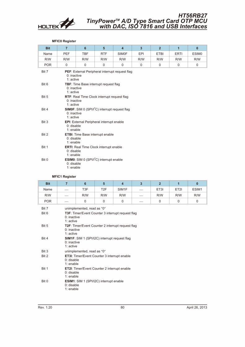
MFIC0 Register
Bit 7 6 5 4 3 2 1 0
Name PEF TBF RTF SIM0F EPI ETBI ERTI ESIM0
R/W R/W R/W R/W R/W R/W R/W R/W R/W
POR 0 0 0 0 0 0 0 0
Bit 7 PEF: External Peripheral interrupt request flag0: inactive1: active
Bit 6 TBF: Time Base interrupt request flag0: inactive1: active
Bit 5 RTF: Real Time Clock interrupt request flag0: inactive1: active
Bit 4 SIM0F: SIM 0 (SPI/I2C) interrupt request flag
0: inactive1: active
Bit 3 EPI: External Peripheral interrupt enable0: disable1: enable
Bit 2 ETBI: Time Base interrupt enable0: disable1: enable
Bit 1 ERTI: Real Time Clock interrupt enable0: disable1: enable
Bit 0 ESIM0: SIM 0 (SPI/I2C) interrupt enable
0: disable1: enable
MFIC1 Register
Bit 7 6 5 4 3 2 1 0
Name � T3F T2F SIM1F � ET3I ET2I ESIM1
R/W � R/W R/W R/W � R/W R/W R/W
POR � 0 0 0 � 0 0 0
Bit 7 unimplemented, read as �0�
Bit 6 T3F: Timer/Event Counter 3 interrupt request flag0: inactive1: active
Bit 5 T2F: Timer/Event Counter 2 interrupt request flag0: inactive1: active
Bit 4 SIM1F: SIM 1 (SPI/I2C) interrupt request flag0: inactive1: active
Bit 3 unimplemented, read as �0�
Bit 2 ET3I: Timer/Event Counter 3 interrupt enable0: disable1: enable
Bit 1 ET2I: Timer/Event Counter 2 interrupt enable0: disable1: enable
Bit 0 ESIM1: SIM 1 (SPI/I2C) interrupt enable0: disable1: enable
Rev. 1.20 80 April 26, 2013
HT56RB27TinyPowerTM A/D Type Smart Card OTP MCU
with DAC, ISO 7816 and USB Interfaces
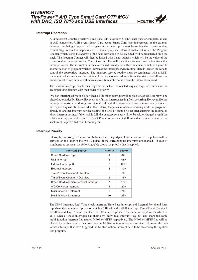
Interrupt Operation
A Timer/Event Counter overflow, Time Base, RTC overflow, SPI/I2C data transfer complete, an end
of A/D conversion, USB event, Smart Card event, Smart Card insertion/removal or the external
interrupt line being triggered will all generate an interrupt request by setting their corresponding
request flag. When this happens and if their appropriate interrupt enable bit is set, the Program
Counter, which stores the address of the next instruction to be executed, will be transferred onto the
stack. The Program Counter will then be loaded with a new address which will be the value of the
corresponding interrupt vector. The microcontroller will then fetch its next instruction from this
interrupt vector. The instruction at this vector will usually be a JMP statement which will jump to
another section of program which is known as the interrupt service routine. Here is located the code to
control the appropriate interrupt. The interrupt service routine must be terminated with a RETI
statement, which retrieves the original Program Counter address from the stack and allows the
microcontroller to continue with normal execution at the point where the interrupt occurred.
The various interrupt enable bits, together with their associated request flags, are shown in the
accompanying diagram with their order of priority.
Once an interrupt subroutine is serviced, all the other interrupts will be blocked, as the EMI bit will be
cleared automatically. This will prevent any further interrupt nesting from occurring. However, if other
interrupt requests occur during this interval, although the interrupt will not be immediately serviced,
the request flag will still be recorded. If an interrupt requires immediate servicing while the program is
already in another interrupt service routine, the EMI bit should be set after entering the routine, to
allow interrupt nesting. If the stack is full, the interrupt request will not be acknowledged, even if the
related interrupt is enabled, until the Stack Pointer is decremented. If immediate service is desired, the
stack must be prevented from becoming full.
Interrupt Priority
Interrupts, occurring in the interval between the rising edges of two consecutive T2 pulses, will be
serviced on the latter of the two T2 pulses, if the corresponding interrupts are enabled. In case of
simultaneous requests, the following table shows the priority that is applied.
Interrupt Source Priority Vector
Smart Card Interrupt 1 04H
USB Interrupt 2 08H
External Interrupt 0 3 0CH
External Interrupt 1 4 10H
Timer/Event Counter 0 Overflow 5 14H
Timer/Event Counter 1 Overflow 6 18H
Smart Card Insertion/Removal Interrupt 7 1CH
A/D Converter Interrupt 8 20H
Multi-function 0 Interrupt 9 24H
Multi-function 1 Interrupt 10 28H
The SIM0 interrupt, Real Time clock interrupt, Time Base interrupt and External Peripheral inter-
rupt share the same interrupt vector which is 24H while the SIM1 interrupt, Timer/Event Counter 2
overflow and Timer/Event Counter 3 overflow interrupt share the same interrupt vector which is
28H. Each of these interrupts has their own individual interrupt flag but also share the same
multi-function interrupt flag named MF0F or MF1F respectively. The MF0F or MF1F flag will be
cleared by hardware once the corresponding Multi-function interrupt is serviced. However the indi-
vidual interrupts that have triggered the Multi-function interrupt need to be cleared by the applica-
tion program.
HT56RB27TinyPowerTM A/D Type Smart Card OTP MCUwith DAC, ISO 7816 and USB Interfaces
Rev. 1.20 81 April 26, 2013
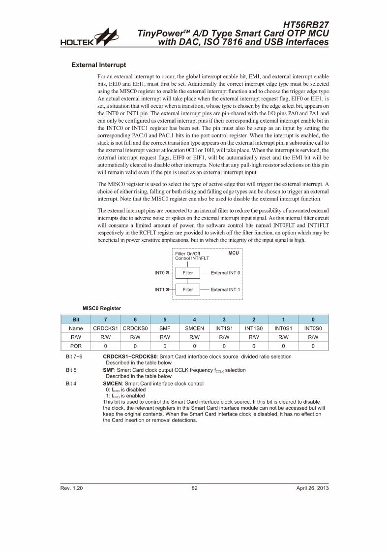
External Interrupt
For an external interrupt to occur, the global interrupt enable bit, EMI, and external interrupt enable
bits, EEI0 and EEI1, must first be set. Additionally the correct interrupt edge type must be selected
using the MISC0 register to enable the external interrupt function and to choose the trigger edge type.
An actual external interrupt will take place when the external interrupt request flag, EIF0 or EIF1, is
set, a situation that will occur when a transition, whose type is chosen by the edge select bit, appears on
the INT0 or INT1 pin. The external interrupt pins are pin-shared with the I/O pins PA0 and PA1 and
can only be configured as external interrupt pins if their corresponding external interrupt enable bit in
the INTC0 or INTC1 register has been set. The pin must also be setup as an input by setting the
corresponding PAC.0 and PAC.1 bits in the port control register. When the interrupt is enabled, the
stack is not full and the correct transition type appears on the external interrupt pin, a subroutine call to
the external interrupt vector at location 0CH or 10H, will take place. When the interrupt is serviced, the
external interrupt request flags, EIF0 or EIF1, will be automatically reset and the EMI bit will be
automatically cleared to disable other interrupts. Note that any pull-high resistor selections on this pin
will remain valid even if the pin is used as an external interrupt input.
The MISC0 register is used to select the type of active edge that will trigger the external interrupt. A
choice of either rising, falling or both rising and falling edge types can be chosen to trigger an external
interrupt. Note that the MISC0 register can also be used to disable the external interrupt function.
The external interrupt pins are connected to an internal filter to reduce the possibility of unwanted external
interrupts due to adverse noise or spikes on the external interrupt input signal. As this internal filter circuit
will consume a limited amount of power, the software control bits named INT0FLT and INT1FLT
respectively in the RCFLT register are provided to switch off the filter function, an option which may be
beneficial in power sensitive applications, but in which the integrity of the input signal is high.
MISC0 Register
Bit 7 6 5 4 3 2 1 0
Name CRDCKS1 CRDCKS0 SMF SMCEN INT1S1 INT1S0 INT0S1 INT0S0
R/W R/W R/W R/W R/W R/W R/W R/W R/W
POR 0 0 0 0 0 0 0 0
Bit 7~6 CRDCKS1~CRDCKS0: Smart Card interface clock source divided ratio selectionDescribed in the table below
Bit 5 SMF: Smart Card clock output CCLK frequency fCCLK selectionDescribed in the table below
Bit 4 SMCEN: Smart Card interface clock control0: fCRD is disabled1: fCRD is enabled
This bit is used to control the Smart Card interface clock source. If this bit is cleared to disablethe clock, the relevant registers in the Smart Card interface module can not be accessed but willkeep the original contents. When the Smart Card interface clock is disabled, it has no effect onthe Card insertion or removal detections.
Rev. 1.20 82 April 26, 2013
HT56RB27TinyPowerTM A/D Type Smart Card OTP MCU
with DAC, ISO 7816 and USB Interfaces
� � � � � ! � � = : :� � � ! � � � 4 � � � + �
� 4 � �
� � � � � !� 4 � 7
� � � � � !
� � � � ! � � � � � 4 � � 7
� � � � ! � � � � � 4 � � �
� �
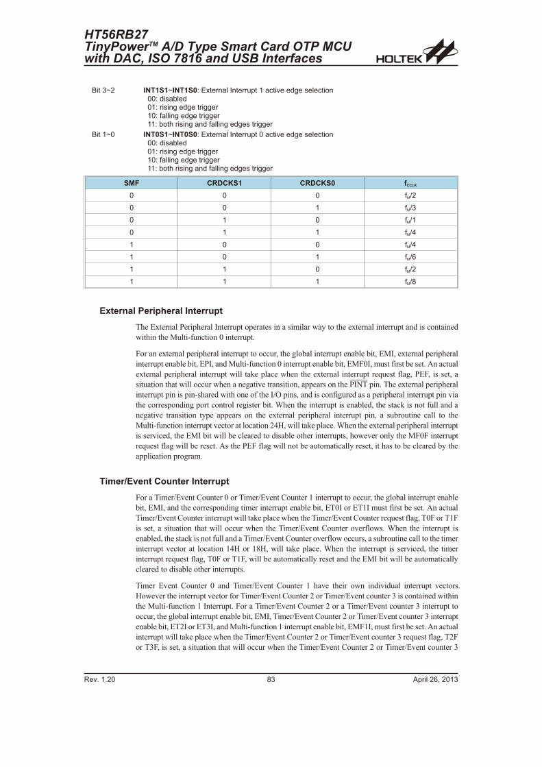
Bit 3~2 INT1S1~INT1S0: External Interrupt 1 active edge selection00: disabled01: rising edge trigger10: falling edge trigger11: both rising and falling edges trigger
Bit 1~0 INT0S1~INT0S0: External Interrupt 0 active edge selection00: disabled01: rising edge trigger10: falling edge trigger11: both rising and falling edges trigger
SMF CRDCKS1 CRDCKS0 fCCLK
0 0 0 fM/2
0 0 1 fM/3
0 1 0 fM/1
0 1 1 fM/4
1 0 0 fM/4
1 0 1 fM/6
1 1 0 fM/2
1 1 1 fM/8
External Peripheral Interrupt
The External Peripheral Interrupt operates in a similar way to the external interrupt and is contained
within the Multi-function 0 interrupt.
For an external peripheral interrupt to occur, the global interrupt enable bit, EMI, external peripheral
interrupt enable bit, EPI, and Multi-function 0 interrupt enable bit, EMF0I, must first be set. An actual
external peripheral interrupt will take place when the external interrupt request flag, PEF, is set, a
situation that will occur when a negative transition, appears on the PINT pin. The external peripheral
interrupt pin is pin-shared with one of the I/O pins, and is configured as a peripheral interrupt pin via
the corresponding port control register bit. When the interrupt is enabled, the stack is not full and a
negative transition type appears on the external peripheral interrupt pin, a subroutine call to the
Multi-function interrupt vector at location 24H, will take place. When the external peripheral interrupt
is serviced, the EMI bit will be cleared to disable other interrupts, however only the MF0F interrupt
request flag will be reset. As the PEF flag will not be automatically reset, it has to be cleared by the
application program.
Timer/Event Counter Interrupt
For a Timer/Event Counter 0 or Timer/Event Counter 1 interrupt to occur, the global interrupt enable
bit, EMI, and the corresponding timer interrupt enable bit, ET0I or ET1I must first be set. An actual
Timer/Event Counter interrupt will take place when the Timer/Event Counter request flag, T0F or T1F
is set, a situation that will occur when the Timer/Event Counter overflows. When the interrupt is
enabled, the stack is not full and a Timer/Event Counter overflow occurs, a subroutine call to the timer
interrupt vector at location 14H or 18H, will take place. When the interrupt is serviced, the timer
interrupt request flag, T0F or T1F, will be automatically reset and the EMI bit will be automatically
cleared to disable other interrupts.
Timer Event Counter 0 and Timer/Event Counter 1 have their own individual interrupt vectors.
However the interrupt vector for Timer/Event Counter 2 or Timer/Event counter 3 is contained within
the Multi-function 1 Interrupt. For a Timer/Event Counter 2 or a Timer/Event counter 3 interrupt to
occur, the global interrupt enable bit, EMI, Timer/Event Counter 2 or Timer/Event counter 3 interrupt
enable bit, ET2I or ET3I, and Multi-function 1 interrupt enable bit, EMF1I, must first be set. An actual
interrupt will take place when the Timer/Event Counter 2 or Timer/Event counter 3 request flag, T2F
or T3F, is set, a situation that will occur when the Timer/Event Counter 2 or Timer/Event counter 3
HT56RB27TinyPowerTM A/D Type Smart Card OTP MCUwith DAC, ISO 7816 and USB Interfaces
Rev. 1.20 83 April 26, 2013
overflows. When the interrupt is enabled, the stack is not full and the Timer/Event Counter 2 or
Timer/Event counter 3 overflows, a subroutine call to the Multi-function interrupt vector at location
28H, will take place. When the Timer/Event 2 or Timer/Event counter 3 interrupt is serviced, the EMI
bit will be cleared to disable other interrupts, however only the MFF interrupt request flag will be reset.
As the T2F or T3F flag will not be automatically reset, it has to be cleared by the application program.
A/D Interrupt
The A/D Interrupt is contained within the Multi-function Interrupt.
For an A/D Interrupt to be generated, the global interrupt enable bit EMI and the A/D Interrupt enable
bit EADI must first be set. An actual A/D Interrupt will take place when the A/D Interrupt request flag,
ADF, is set, a situation that will occur when the A/D conversion process has finished. When the
interrupt is enabled, the stack is not full and the A/D conversion process has ended, a subroutine call to
the A/D interrupt vector at location 20H, will take place. When the A/D Interrupt is serviced, the A/D
interrupt request flag ADF will be automatically reset and the EMI bit will be automatically cleared to
disable other interrupts.
Smart Card Interrupt
For a Smart Card Interrupt to be generated, the global interrupt enable bit EMI must first be set as well
as one of the associated Smart Card event Interrupt enable bits. The Smart Card events that will
generate an interrupt include situations such as a Card voltage error, a Card current overload, a waiting
timer overflow, a parity error, a transmit buffer empty or an end of transmission or reception. Once one
of the associated Smart Card event interrupt enable control bits is set, it will automatically set the
CRDE bit to 1 to enable the related Smart Card interrupt. An actual Smart Card Interrupt will take
place when the Smart Card Interrupt request flag, CRDF, is set, a situation that will occur when a Smart
Card event has occurred. When the interrupt is enabled, the stack is not full and a Smart Card event has
occurred, a subroutine call to the Smart Card interrupt vector at location 04H, will take place. When
the Smart Card Interrupt is serviced, the Smart Card interrupt request flag CRDF will be automatically
reset and the EMI bit will be automatically cleared to disable other interrupts.
Smart Card Insertion/Removal Interrupt
For a Smart Card Insertion/Removal Interrupt to be generated, the global interrupt enable bit EMI and
the Smart Card Insertion/Removal interrupt enable bit CIRE must first be set. An actual Smart Card
Insertion/Removal Interrupt will take place when the Smart Card Insertion/Removal Interrupt request
flag, SCIRF, is set, a situation that will occur when the Smart Card has been inserted or removed.
When the interrupt is enabled, the stack is not full and the Smart Card has been inserted or removed, a
subroutine call to the Smart Card Insertion/Removal Interrupt vector at location 1CH, will take place.
When the Smart Card Insertion/Removal Interrupt is serviced, the Smart Card Insertion/Removal
interrupt request flag SCIRF will be automatically reset and the EMI bit will be automatically cleared
to disable other interrupts.
SIM (SPI/I2C Interface) Interrupts
The two SIM (SPI/I2C ) interrupts named SIM0 interrupt and SIM1 interrupt are contained within the
Multi-function 0 Interrupt and Multi-function 1 Interrupt respectively.
For an SIM (SPI/I2C interface) interrupt to occur, the global interrupt enable bit named EMI, the
associated SIM interrupt enable control bit named ESIM0 or ESIM1 and the Multi-function interrupt
enable bit named EMF0I or EMF1I must be first set. An actual SIM (SPI/I2C interface) interrupt will
take place when the SIM (SPI/I2C interface) request flag, SIM0F or SIM1F, is set, a situation that will
occur when a byte of data has been transmitted or received by the SPI/I2C interface or when an I
2C
address match occurs. When the interrupt is enabled, the stack is not full and a byte of data has been
Rev. 1.20 84 April 26, 2013
HT56RB27TinyPowerTM A/D Type Smart Card OTP MCU
with DAC, ISO 7816 and USB Interfaces
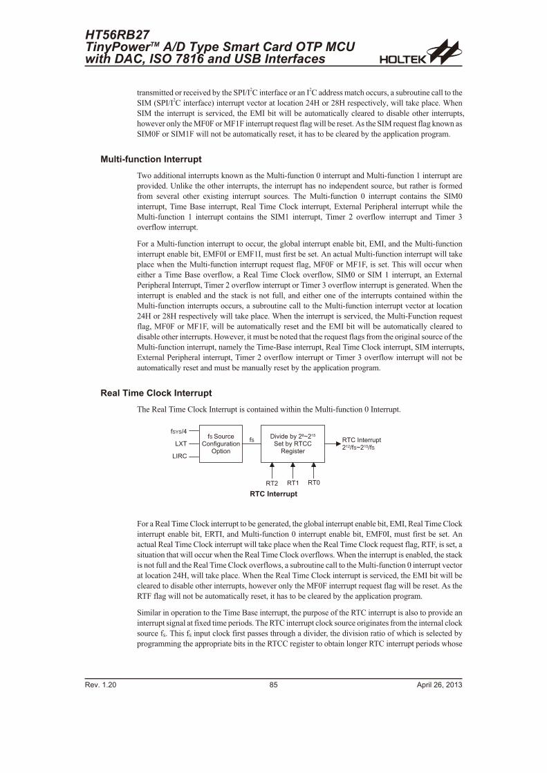
transmitted or received by the SPI/I2C interface or an I
2C address match occurs, a subroutine call to the
SIM (SPI/I2C interface) interrupt vector at location 24H or 28H respectively, will take place. When
SIM the interrupt is serviced, the EMI bit will be automatically cleared to disable other interrupts,
however only the MF0F or MF1F interrupt request flag will be reset. As the SIM request flag known as
SIM0F or SIM1F will not be automatically reset, it has to be cleared by the application program.
Multi-function Interrupt
Two additional interrupts known as the Multi-function 0 interrupt and Multi-function 1 interrupt are
provided. Unlike the other interrupts, the interrupt has no independent source, but rather is formed
from several other existing interrupt sources. The Multi-function 0 interrupt contains the SIM0
interrupt, Time Base interrupt, Real Time Clock interrupt, External Peripheral interrupt while the
Multi-function 1 interrupt contains the SIM1 interrupt, Timer 2 overflow interrupt and Timer 3
overflow interrupt.
For a Multi-function interrupt to occur, the global interrupt enable bit, EMI, and the Multi-function
interrupt enable bit, EMF0I or EMF1I, must first be set. An actual Multi-function interrupt will take
place when the Multi-function interrupt request flag, MF0F or MF1F, is set. This will occur when
either a Time Base overflow, a Real Time Clock overflow, SIM0 or SIM 1 interrupt, an External
Peripheral Interrupt, Timer 2 overflow interrupt or Timer 3 overflow interrupt is generated. When the
interrupt is enabled and the stack is not full, and either one of the interrupts contained within the
Multi-function interrupts occurs, a subroutine call to the Multi-function interrupt vector at location
24H or 28H respectively will take place. When the interrupt is serviced, the Multi-Function request
flag, MF0F or MF1F, will be automatically reset and the EMI bit will be automatically cleared to
disable other interrupts. However, it must be noted that the request flags from the original source of the
Multi-function interrupt, namely the Time-Base interrupt, Real Time Clock interrupt, SIM interrupts,
External Peripheral interrupt, Timer 2 overflow interrupt or Timer 3 overflow interrupt will not be
automatically reset and must be manually reset by the application program.
Real Time Clock Interrupt
The Real Time Clock Interrupt is contained within the Multi-function 0 Interrupt.
For a Real Time Clock interrupt to be generated, the global interrupt enable bit, EMI, Real Time Clock
interrupt enable bit, ERTI, and Multi-function 0 interrupt enable bit, EMF0I, must first be set. An
actual Real Time Clock interrupt will take place when the Real Time Clock request flag, RTF, is set, a
situation that will occur when the Real Time Clock overflows. When the interrupt is enabled, the stack
is not full and the Real Time Clock overflows, a subroutine call to the Multi-function 0 interrupt vector
at location 24H, will take place. When the Real Time Clock interrupt is serviced, the EMI bit will be
cleared to disable other interrupts, however only the MF0F interrupt request flag will be reset. As the
RTF flag will not be automatically reset, it has to be cleared by the application program.
Similar in operation to the Time Base interrupt, the purpose of the RTC interrupt is also to provide an
interrupt signal at fixed time periods. The RTC interrupt clock source originates from the internal clock
source fS. This fS input clock first passes through a divider, the division ratio of which is selected by
programming the appropriate bits in the RTCC register to obtain longer RTC interrupt periods whose
HT56RB27TinyPowerTM A/D Type Smart Card OTP MCUwith DAC, ISO 7816 and USB Interfaces
Rev. 1.20 85 April 26, 2013
: # � # � ! �� � : � % � ! � � � �
( � � �
: # - # = '
+ D �
+ � �
� � 9 � ; � � < $ � � 6 G � � )
# � � � < $ � � � � � % � � � � !
: # � � � � � � � ! ! � ( �� � � = : # G � � ) = : #
� � � � � 7
RTC Interrupt
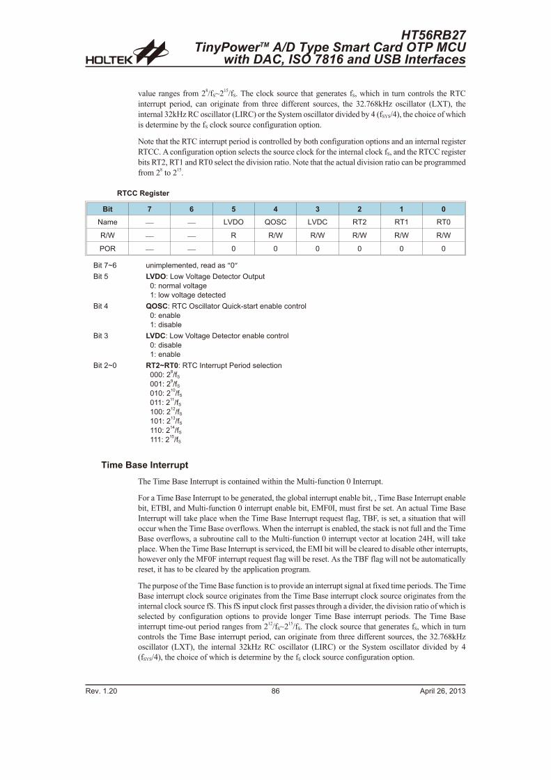
value ranges from 28/fS~2
15/fS. The clock source that generates fS, which in turn controls the RTC
interrupt period, can originate from three different sources, the 32.768kHz oscillator (LXT), the
internal 32kHz RC oscillator (LIRC) or the System oscillator divided by 4 (fSYS/4), the choice of which
is determine by the fS clock source configuration option.
Note that the RTC interrupt period is controlled by both configuration options and an internal register
RTCC. A configuration option selects the source clock for the internal clock fS, and the RTCC register
bits RT2, RT1 and RT0 select the division ratio. Note that the actual division ratio can be programmed
from 28
to 215
.
RTCC Register
Bit 7 6 5 4 3 2 1 0
Name � � LVDO QOSC LVDC RT2 RT1 RT0
R/W � � R R/W R/W R/W R/W R/W
POR � � 0 0 0 0 0 0
Bit 7~6 unimplemented, read as �0�
Bit 5 LVDO: Low Voltage Detector Output
0: normal voltage
1: low voltage detected
Bit 4 QOSC: RTC Oscillator Quick-start enable control
0: enable
1: disable
Bit 3 LVDC: Low Voltage Detector enable control
0: disable
1: enable
Bit 2~0 RT2~RT0: RTC Interrupt Period selection
000: 28/fS
001: 29/fS
010: 210
/fS
011: 211
/fS
100: 212
/fS
101: 213
/fS
110: 214
/fS
111: 215
/fS
Time Base Interrupt
The Time Base Interrupt is contained within the Multi-function 0 Interrupt.
For a Time Base Interrupt to be generated, the global interrupt enable bit, , Time Base Interrupt enable
bit, ETBI, and Multi-function 0 interrupt enable bit, EMF0I, must first be set. An actual Time Base
Interrupt will take place when the Time Base Interrupt request flag, TBF, is set, a situation that will
occur when the Time Base overflows. When the interrupt is enabled, the stack is not full and the Time
Base overflows, a subroutine call to the Multi-function 0 interrupt vector at location 24H, will take
place. When the Time Base Interrupt is serviced, the EMI bit will be cleared to disable other interrupts,
however only the MF0F interrupt request flag will be reset. As the TBF flag will not be automatically
reset, it has to be cleared by the application program.
The purpose of the Time Base function is to provide an interrupt signal at fixed time periods. The Time
Base interrupt clock source originates from the Time Base interrupt clock source originates from the
internal clock source fS. This fS input clock first passes through a divider, the division ratio of which is
selected by configuration options to provide longer Time Base interrupt periods. The Time Base
interrupt time-out period ranges from 212
/fS~215
/fS. The clock source that generates fS, which in turn
controls the Time Base interrupt period, can originate from three different sources, the 32.768kHz
oscillator (LXT), the internal 32kHz RC oscillator (LIRC) or the System oscillator divided by 4
(fSYS/4), the choice of which is determine by the fS clock source configuration option.
Rev. 1.20 86 April 26, 2013
HT56RB27TinyPowerTM A/D Type Smart Card OTP MCU
with DAC, ISO 7816 and USB Interfaces
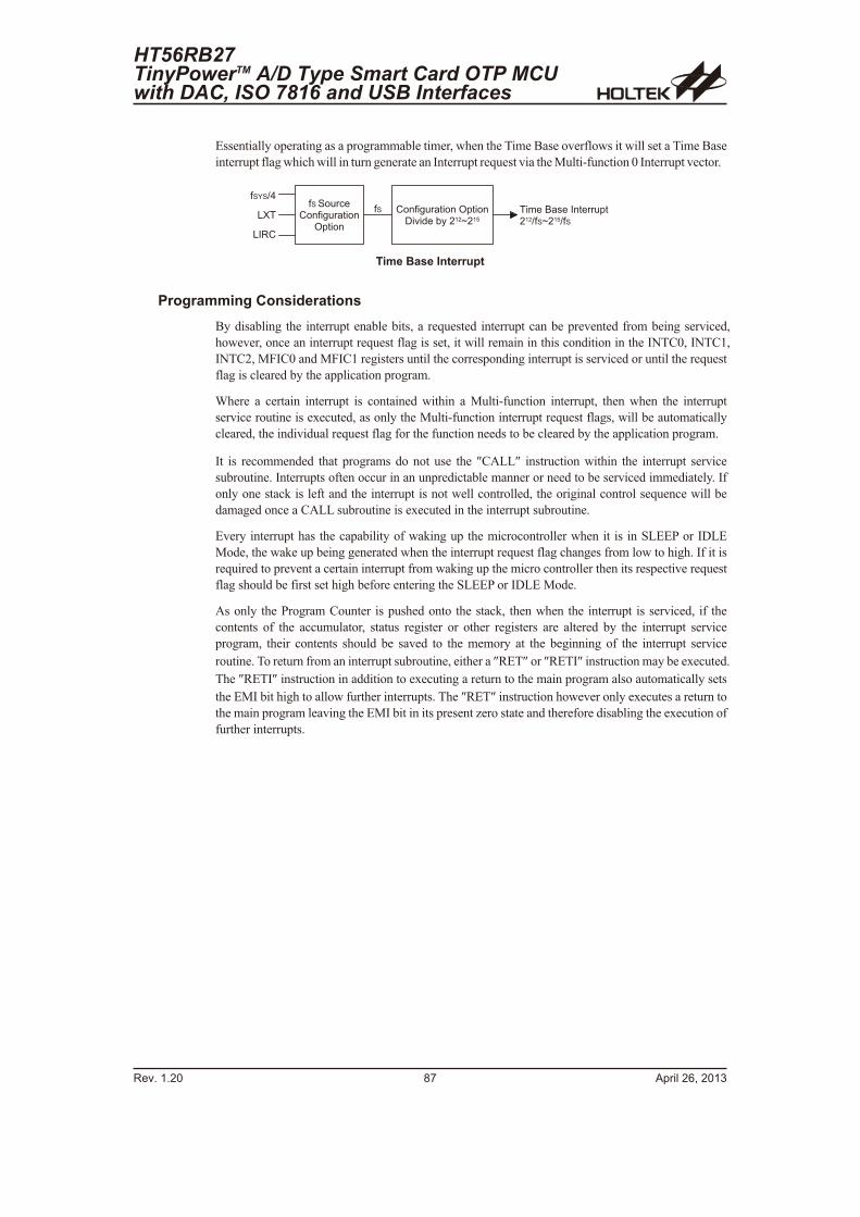
Essentially operating as a programmable timer, when the Time Base overflows it will set a Time Base
interrupt flag which will in turn generate an Interrupt request via the Multi-function 0 Interrupt vector.
Programming Considerations
By disabling the interrupt enable bits, a requested interrupt can be prevented from being serviced,
however, once an interrupt request flag is set, it will remain in this condition in the INTC0, INTC1,
INTC2, MFIC0 and MFIC1 registers until the corresponding interrupt is serviced or until the request
flag is cleared by the application program.
Where a certain interrupt is contained within a Multi-function interrupt, then when the interrupt
service routine is executed, as only the Multi-function interrupt request flags, will be automatically
cleared, the individual request flag for the function needs to be cleared by the application program.
It is recommended that programs do not use the �CALL� instruction within the interrupt service
subroutine. Interrupts often occur in an unpredictable manner or need to be serviced immediately. If
only one stack is left and the interrupt is not well controlled, the original control sequence will be
damaged once a CALL subroutine is executed in the interrupt subroutine.
Every interrupt has the capability of waking up the microcontroller when it is in SLEEP or IDLE
Mode, the wake up being generated when the interrupt request flag changes from low to high. If it is
required to prevent a certain interrupt from waking up the micro controller then its respective request
flag should be first set high before entering the SLEEP or IDLE Mode.
As only the Program Counter is pushed onto the stack, then when the interrupt is serviced, if the
contents of the accumulator, status register or other registers are altered by the interrupt service
program, their contents should be saved to the memory at the beginning of the interrupt service
routine. To return from an interrupt subroutine, either a �RET� or �RETI� instruction may be executed.
The �RETI� instruction in addition to executing a return to the main program also automatically sets
the EMI bit high to allow further interrupts. The �RET� instruction however only executes a return to
the main program leaving the EMI bit in its present zero state and therefore disabling the execution of
further interrupts.
HT56RB27TinyPowerTM A/D Type Smart Card OTP MCUwith DAC, ISO 7816 and USB Interfaces
Rev. 1.20 87 April 26, 2013
: # � # � ! �� � : � % � ! � � � �
( � � �
: # - # = '
+ D �
+ � �
� � : � % � ! � � � � � ( � � �� � 9 � ; � � < $ � � � � G � � )
: # � � � � � 8 � � � � � � � � ! ! � ( �� � � = : # G � � ) = : #
Time Base Interrupt
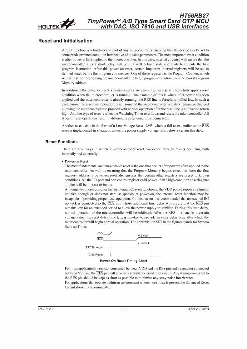
Reset and Initialisation
A reset function is a fundamental part of any microcontroller ensuring that the device can be set to
some predetermined condition irrespective of outside parameters. The most important reset condition
is after power is first applied to the microcontroller. In this case, internal circuitry will ensure that the
microcontroller, after a short delay, will be in a well defined state and ready to execute the first
program instruction. After this power-on reset, certain important internal registers will be set to
defined states before the program commences. One of these registers is the Program Counter, which
will be reset to zero forcing the microcontroller to begin program execution from the lowest Program
Memory address.
In addition to the power-on reset, situations may arise where it is necessary to forcefully apply a reset
condition when the microcontroller is running. One example of this is where after power has been
applied and the microcontroller is already running, the RES line is forcefully pulled low. In such a
case, known as a normal operation reset, some of the microcontroller registers remain unchanged
allowing the microcontroller to proceed with normal operation after the reset line is allowed to return
high. Another type of reset is when the Watchdog Timer overflows and resets the microcontroller. All
types of reset operations result in different register conditions being setup.
Another reset exists in the form of a Low Voltage Reset, LVR, where a full reset, similar to the RES
reset is implemented in situations where the power supply voltage falls below a certain threshold.
Reset Functions
There are five ways in which a microcontroller reset can occur, through events occurring both
internally and externally:
� Power-on Reset
The most fundamental and unavoidable reset is the one that occurs after power is first applied to the
microcontroller. As well as ensuring that the Program Memory begins execution from the first
memory address, a power-on reset also ensures that certain other registers are preset to known
conditions. All the I/O port and port control registers will power up in a high condition ensuring that
all pins will be first set to inputs.
Although the microcontroller has an internal RC reset function, if the VDD power supply rise time is
not fast enough or does not stabilise quickly at power-on, the internal reset function may be
incapable of providing proper reset operation. For this reason it is recommended that an external RC
network is connected to the RES pin, whose additional time delay will ensure that the RES pin
remains low for an extended period to allow the power supply to stabilise. During this time delay,
normal operation of the microcontroller will be inhibited. After the RES line reaches a certain
voltage value, the reset delay time tRSTD is invoked to provide an extra delay time after which the
microcontroller will begin normal operation. The abbreviation SST in the figures stands for System
Start-up Timer.
For most applications a resistor connected between VDD and the RES pin and a capacitor connected
between VSS and the RES pin will provide a suitable external reset circuit. Any wiring connected to
the RES pin should be kept as short as possible to minimise any stray noise interference.
For applications that operate within an environment where more noise is present the Enhanced Reset
Circuit shown is recommended.
Rev. 1.20 88 April 26, 2013
HT56RB27TinyPowerTM A/D Type Smart Card OTP MCU
with DAC, ISO 7816 and USB Interfaces
� #
� � �
# # � � � � � � � � �
� � � ( � � � � �
7 � A � � � �
� # � �
Power-On Reset Timing Chart
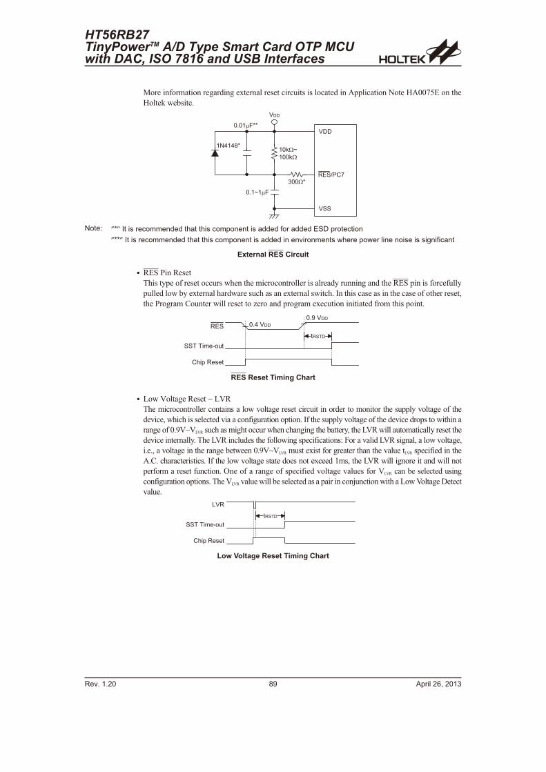
More information regarding external reset circuits is located in Application Note HA0075E on the
Holtek website.
� RES Pin Reset
This type of reset occurs when the microcontroller is already running and the RES pin is forcefully
pulled low by external hardware such as an external switch. In this case as in the case of other reset,
the Program Counter will reset to zero and program execution initiated from this point.
� Low Voltage Reset � LVR
The microcontroller contains a low voltage reset circuit in order to monitor the supply voltage of the
device, which is selected via a configuration option. If the supply voltage of the device drops to within a
range of 0.9V~VLVR such as might occur when changing the battery, the LVR will automatically reset the
device internally. The LVR includes the following specifications: For a valid LVR signal, a low voltage,
i.e., a voltage in the range between 0.9V~VLVR must exist for greater than the value tLVR specified in the
A.C. characteristics. If the low voltage state does not exceed 1ms, the LVR will ignore it and will not
perform a reset function. One of a range of specified voltage values for VLVR can be selected using
configuration options. The VLVR value will be selected as a pair in conjunction with a Low Voltage Detect
value.
HT56RB27TinyPowerTM A/D Type Smart Card OTP MCUwith DAC, ISO 7816 and USB Interfaces
Rev. 1.20 89 April 26, 2013
� # = � � 5
7 � � G � � �
� 7 " � G
� 7 7 " �
� � �
� # #
7 � 7 � � � J J
� � �
� 4 ' � ' 6 J
& 7 7 � J
Note: �*� It is recommended that this component is added for added ESD protection
�**� It is recommended that this component is added in environments where power line noise is significant
External RES Circuit
� #
# # � � � � � � � � �
� � � ( � � � � �
7 � A � � � �
7 � ' � � � �
� # � �
RES Reset Timing Chart
+ �
# # � � � � � � � � �
� � � ( � � � � �
� # � �
Low Voltage Reset Timing Chart
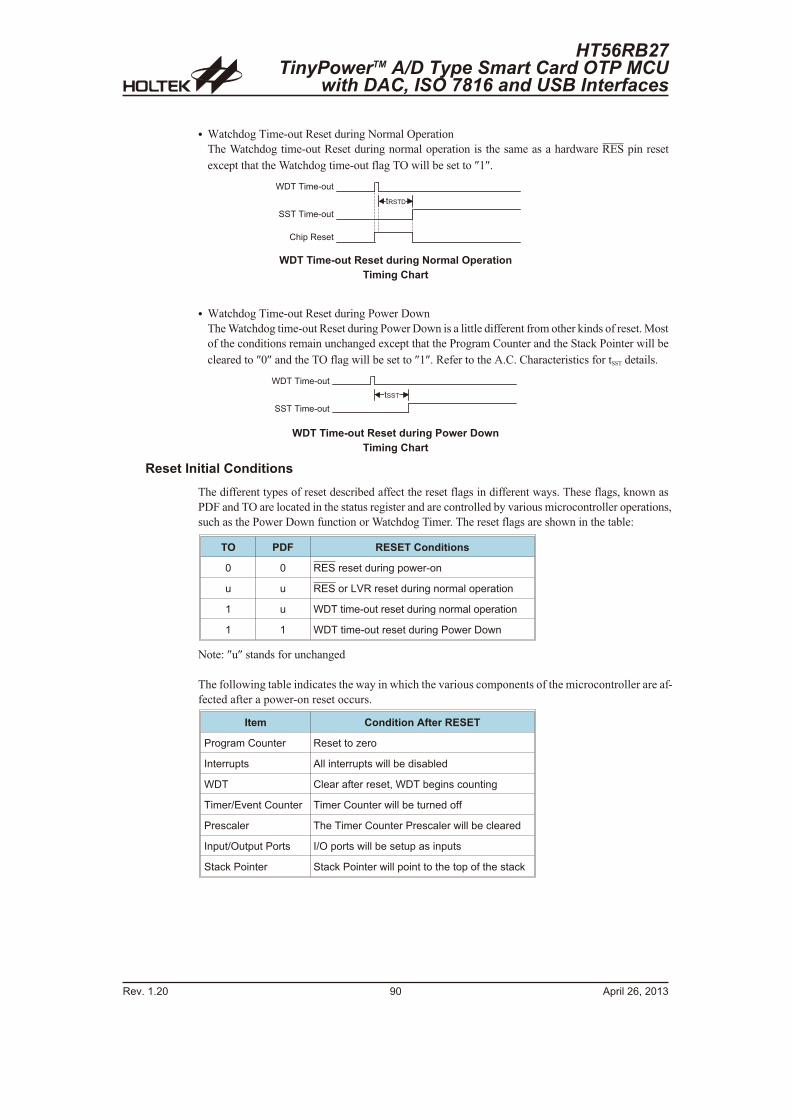
� Watchdog Time-out Reset during Normal Operation
The Watchdog time-out Reset during normal operation is the same as a hardware RES pin reset
except that the Watchdog time-out flag TO will be set to �1�.
� Watchdog Time-out Reset during Power Down
The Watchdog time-out Reset during Power Down is a little different from other kinds of reset. Most
of the conditions remain unchanged except that the Program Counter and the Stack Pointer will be
cleared to �0� and the TO flag will be set to �1�. Refer to the A.C. Characteristics for tSST details.
Reset Initial Conditions
The different types of reset described affect the reset flags in different ways. These flags, known as
PDF and TO are located in the status register and are controlled by various microcontroller operations,
such as the Power Down function or Watchdog Timer. The reset flags are shown in the table:
TO PDF RESET Conditions
0 0 RES reset during power-on
u u RES or LVR reset during normal operation
1 u WDT time-out reset during normal operation
1 1 WDT time-out reset during Power Down
Note: �u� stands for unchanged
The following table indicates the way in which the various components of the microcontroller are af-
fected after a power-on reset occurs.
Item Condition After RESET
Program Counter Reset to zero
Interrupts All interrupts will be disabled
WDT Clear after reset, WDT begins counting
Timer/Event Counter Timer Counter will be turned off
Prescaler The Timer Counter Prescaler will be cleared
Input/Output Ports I/O ports will be setup as inputs
Stack Pointer Stack Pointer will point to the top of the stack
Rev. 1.20 90 April 26, 2013
HT56RB27TinyPowerTM A/D Type Smart Card OTP MCU
with DAC, ISO 7816 and USB Interfaces
C � � � � � � � � � �
# # � � � � � � � � �
� � � ( � � � � �
� # � �
WDT Time-out Reset during Normal Operation
Timing Chart
C � � � � � � � � � �
# # � � � � � � � � �
� # # �
WDT Time-out Reset during Power Down
Timing Chart

The different kinds of resets all affect the internal registers of the microcontroller in different ways. To
ensure reliable continuation of normal program execution after a reset occurs, it is important to know
what condition the microcontroller is in after a particular reset occurs. The following table describes
how each type of reset affects each of the microcontroller internal registers.
RegisterReset
(Power-on)
RES Reset
(Normal
Operation)
WDT Time-out
(Normal
Operation)
WDT Time-out
(HALT)
USB Reset
(Normal)
USB Reset
(HALT)
MP0 x x x x x x x x u u u u u u u u u u u u u u u u u u u u u u u u u u u u u u u u u u u u u u u u
MP1 x x x x x x x x u u u u u u u u u u u u u u u u u u u u u u u u u u u u u u u u u u u u u u u u
BP 0 0 0 0 0 0 0 0 0 0 0 0 0 0 0 0 0 0 0 0 0 0 0 0 u u u u u u u u 0 0 0 0 0 0 0 0 0 0 0 0 0 0 0 0
ACC x x x x x x x x u u u u u u u u u u u u u u u u u u u u u u u u u u u u u u u u u u u u u u u u
PCL 0 0 0 0 0 0 0 0 0 0 0 0 0 0 0 0 0 0 0 0 0 0 0 0 0 0 0 0 0 0 0 0 0 0 0 0 0 0 0 0 0 0 0 0 0 0 0 0
TBLP x x x x x x x x u u u u u u u u u u u u u u u u u u u u u u u u u u u u u u u u u u u u u u u u
TBLH x x x x x x x x u u u u u u u u u u u u u u u u u u u u u u u u u u u u u u u u u u u u u u u u
RTCC � � 0 0 0 1 1 1 � � 0 0 0 1 1 1 � � 0 0 0 1 1 1 � � u u u u u u � � 0 0 0 1 1 1 � � 0 0 0 1 1 1
STATUS � � 0 0 x x x x � � u u u u u u � � 1 u u u u u � � 1 1 u u u u � � u u u u u u � � 0 1 u u u u
TBHP x x x x x x x x u u u u u u u u u u u u u u u u u u u u u u u u u u u u u u u u u u u u u u u u
MISC0 0 0 0 0 0 0 0 0 0 0 0 0 0 0 0 0 0 0 0 0 0 0 0 0 u u u u u u u u 0 0 0 0 0 0 0 0 0 0 0 0 0 0 0 0
MISC1 0 0 0 0 1 0 1 0 0 0 0 0 1 0 1 0 0 0 0 0 1 0 1 0 u u u u u u u u 0 0 0 0 1 0 1 0 0 0 0 0 1 0 1 0
CLKMOD 0 0 0 0 0 x 1 1 0 0 0 0 0 x 1 1 0 0 0 0 0 x 1 1 u u u u u u u u 0 0 0 0 0 x 1 1 0 0 0 0 0 x 1 1
DC2DC � � � � � � 0 0 � � � � � � 0 0 � � � � � � 0 0 � � � � � � u u � � � � � � 0 0 � � � � � � 0 0
INTC0 � 0 0 0 0 0 0 0 � 0 0 0 0 0 0 0 � 0 0 0 0 0 0 0 � u u u u u u u � 0 0 0 0 0 0 0 � 0 0 0 0 0 0 0
INTC1 � 0 0 0 0 0 0 0 � 0 0 0 0 0 0 0 � 0 0 0 0 0 0 0 � u u u u u u u � 0 0 0 0 0 0 0 � 0 0 0 0 0 0 0
INTC2 � � 0 0 � � 0 0 � � 0 0 � � 0 0 � � 0 0 � � 0 0 � � u u � � u u � � 0 0 � � 0 0 � � 0 0 � � 0 0
MFIC0 0 0 0 0 0 0 0 0 0 0 0 0 0 0 0 0 0 0 0 0 0 0 0 0 u u u u u u u u 0 0 0 0 0 0 0 0 0 0 0 0 0 0 0 0
MFIC1 � 0 0 0 � 0 0 0 � 0 0 0 � 0 0 0 � 0 0 0 � 0 0 0 � u u u � u u u � 0 0 0 � 0 0 0 � 0 0 0 � 0 0 0
PAWU 0 0 0 0 0 0 0 0 0 0 0 0 0 0 0 0 0 0 0 0 0 0 0 0 u u u u u u u u 0 0 0 0 0 0 0 0 0 0 0 0 0 0 0 0
PAPU 0 0 0 0 0 0 0 0 0 0 0 0 0 0 0 0 0 0 0 0 0 0 0 0 u u u u u u u u 0 0 0 0 0 0 0 0 0 0 0 0 0 0 0 0
PA 1 1 1 1 1 1 1 1 1 1 1 1 1 1 1 1 1 1 1 1 1 1 1 1 u u u u u u u u 1 1 1 1 1 1 1 1 1 1 1 1 1 1 1 1
PAC 1 1 1 1 1 1 1 1 1 1 1 1 1 1 1 1 1 1 1 1 1 1 1 1 u u u u u u u u 1 1 1 1 1 1 1 1 1 1 1 1 1 1 1 1
PBPU 0 0 0 0 0 0 0 0 0 0 0 0 0 0 0 0 0 0 0 0 0 0 0 0 u u u u u u u u 0 0 0 0 0 0 0 0 0 0 0 0 0 0 0 0
PB 1 1 1 1 1 1 1 1 1 1 1 1 1 1 1 1 1 1 1 1 1 1 1 1 u u u u u u u u 1 1 1 1 1 1 1 1 1 1 1 1 1 1 1 1
PBC 1 1 1 1 1 1 1 1 1 1 1 1 1 1 1 1 1 1 1 1 1 1 1 1 u u u u u u u u 1 1 1 1 1 1 1 1 1 1 1 1 1 1 1 1
PCPU � 0 0 0 0 0 0 0 � 0 0 0 0 0 0 0 � 0 0 0 0 0 0 0 u u u u u u u u � 0 0 0 0 0 0 0 � 0 0 0 0 0 0 0
PC 1 1 1 1 1 1 1 1 1 1 1 1 1 1 1 1 1 1 1 1 1 1 1 1 u u u u u u u u 1 1 1 1 1 1 1 1 1 1 1 1 1 1 1 1
PCC 1 1 1 1 1 1 1 1 1 1 1 1 1 1 1 1 1 1 1 1 1 1 1 1 u u u u u u u u 1 1 1 1 1 1 1 1 1 1 1 1 1 1 1 1
PWM0L 0 0 0 0 � ��� 0 0 0 0 0 � ��� 0 0 0 0 0 � ��� 0 u u u u � ��� u 0 0 0 0 � ��� 0 0 0 0 0 � ��� 0
PWM0H 0 0 0 0 0 0 0 0 0 0 0 0 0 0 0 0 0 0 0 0 0 0 0 0 u u u u u u u u 0 0 0 0 0 0 0 0 0 0 0 0 0 0 0 0
PWM1L 0 0 0 0 � ��� 0 0 0 0 0 � ��� 0 0 0 0 0 � ��� 0 u u u u � ��� u 0 0 0 0 � ��� 0 0 0 0 0 � ��� 0
PWM1H 0 0 0 0 0 0 0 0 0 0 0 0 0 0 0 0 0 0 0 0 0 0 0 0 u u u u u u u u 0 0 0 0 0 0 0 0 0 0 0 0 0 0 0 0
PWM2L 0 0 0 0 � ��� 0 0 0 0 0 � ��� 0 0 0 0 0 � ��� 0 u u u u � ��� u 0 0 0 0 � ��� 0 0 0 0 0 � ��� 0
HT56RB27TinyPowerTM A/D Type Smart Card OTP MCUwith DAC, ISO 7816 and USB Interfaces
Rev. 1.20 91 April 26, 2013
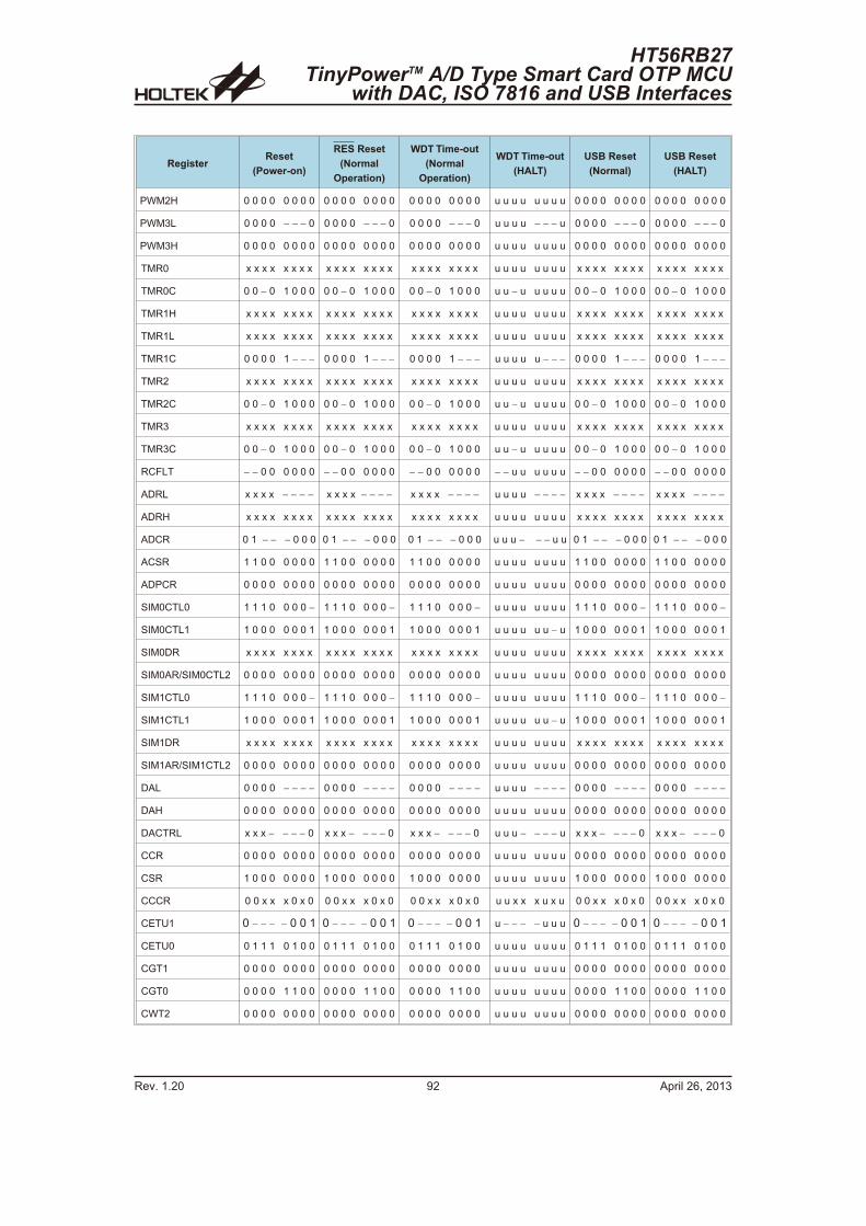
RegisterReset
(Power-on)
RES Reset
(Normal
Operation)
WDT Time-out
(Normal
Operation)
WDT Time-out
(HALT)
USB Reset
(Normal)
USB Reset
(HALT)
PWM2H 0 0 0 0 0 0 0 0 0 0 0 0 0 0 0 0 0 0 0 0 0 0 0 0 u u u u u u u u 0 0 0 0 0 0 0 0 0 0 0 0 0 0 0 0
PWM3L 0 0 0 0 � ��� 0 0 0 0 0 � ��� 0 0 0 0 0 � ��� 0 u u u u � ��� u 0 0 0 0 � ��� 0 0 0 0 0 � ��� 0
PWM3H 0 0 0 0 0 0 0 0 0 0 0 0 0 0 0 0 0 0 0 0 0 0 0 0 u u u u u u u u 0 0 0 0 0 0 0 0 0 0 0 0 0 0 0 0
TMR0 x x x x x x x x x x x x x x x x x x x x x x x x u u u u u u u u x x x x x x x x x x x x x x x x
TMR0C 0 0 � 0 1 0 0 0 0 0 � 0 1 0 0 0 0 0 � 0 1 0 0 0 u u � u u u u u 0 0 � 0 1 0 0 0 0 0 � 0 1 0 0 0
TMR1H x x x x x x x x x x x x x x x x x x x x x x x x u u u u u u u u x x x x x x x x x x x x x x x x
TMR1L x x x x x x x x x x x x x x x x x x x x x x x x u u u u u u u u x x x x x x x x x x x x x x x x
TMR1C 0 0 0 0 1 � ��� 0 0 0 0 1 � ��� 0 0 0 0 1 � ��� u u u u u � ��� 0 0 0 0 1 � ��� 0 0 0 0 1 � ���
TMR2 x x x x x x x x x x x x x x x x x x x x x x x x u u u u u u u u x x x x x x x x x x x x x x x x
TMR2C 0 0 � 0 1 0 0 0 0 0 � 0 1 0 0 0 0 0 � 0 1 0 0 0 u u � u u u u u 0 0 � 0 1 0 0 0 0 0 � 0 1 0 0 0
TMR3 x x x x x x x x x x x x x x x x x x x x x x x x u u u u u u u u x x x x x x x x x x x x x x x x
TMR3C 0 0 � 0 1 0 0 0 0 0 � 0 1 0 0 0 0 0 � 0 1 0 0 0 u u � u u u u u 0 0 � 0 1 0 0 0 0 0 � 0 1 0 0 0
RCFLT � � 0 0 0 0 0 0 � � 0 0 0 0 0 0 � � 0 0 0 0 0 0 � � u u u u u u � � 0 0 0 0 0 0 � � 0 0 0 0 0 0
ADRL x x x x � � � � x x x x � � � � x x x x � � � � u u u u � � � � x x x x � � � � x x x x � � � �
ADRH x x x x x x x x x x x x x x x x x x x x x x x x u u u u u u u u x x x x x x x x x x x x x x x x
ADCR 0 1 ��� � 0 0 0 0 1 ��� � 0 0 0 0 1 ��� � 0 0 0 u u u � ��� u u 0 1 ��� � 0 0 0 0 1 ��� � 0 0 0
ACSR 1 1 0 0 0 0 0 0 1 1 0 0 0 0 0 0 1 1 0 0 0 0 0 0 u u u u u u u u 1 1 0 0 0 0 0 0 1 1 0 0 0 0 0 0
ADPCR 0 0 0 0 0 0 0 0 0 0 0 0 0 0 0 0 0 0 0 0 0 0 0 0 u u u u u u u u 0 0 0 0 0 0 0 0 0 0 0 0 0 0 0 0
SIM0CTL0 1 1 1 0 0 0 0 � 1 1 1 0 0 0 0 � 1 1 1 0 0 0 0 � u u u u u u u u 1 1 1 0 0 0 0 � 1 1 1 0 0 0 0 �
SIM0CTL1 1 0 0 0 0 0 0 1 1 0 0 0 0 0 0 1 1 0 0 0 0 0 0 1 u u u u u u � u 1 0 0 0 0 0 0 1 1 0 0 0 0 0 0 1
SIM0DR x x x x x x x x x x x x x x x x x x x x x x x x u u u u u u u u x x x x x x x x x x x x x x x x
SIM0AR/SIM0CTL2 0 0 0 0 0 0 0 0 0 0 0 0 0 0 0 0 0 0 0 0 0 0 0 0 u u u u u u u u 0 0 0 0 0 0 0 0 0 0 0 0 0 0 0 0
SIM1CTL0 1 1 1 0 0 0 0 � 1 1 1 0 0 0 0 � 1 1 1 0 0 0 0 � u u u u u u u u 1 1 1 0 0 0 0 � 1 1 1 0 0 0 0 �
SIM1CTL1 1 0 0 0 0 0 0 1 1 0 0 0 0 0 0 1 1 0 0 0 0 0 0 1 u u u u u u � u 1 0 0 0 0 0 0 1 1 0 0 0 0 0 0 1
SIM1DR x x x x x x x x x x x x x x x x x x x x x x x x u u u u u u u u x x x x x x x x x x x x x x x x
SIM1AR/SIM1CTL2 0 0 0 0 0 0 0 0 0 0 0 0 0 0 0 0 0 0 0 0 0 0 0 0 u u u u u u u u 0 0 0 0 0 0 0 0 0 0 0 0 0 0 0 0
DAL 0 0 0 0 � � � � 0 0 0 0 � � � � 0 0 0 0 � � � � u u u u � � � � 0 0 0 0 � � � � 0 0 0 0 � � � �
DAH 0 0 0 0 0 0 0 0 0 0 0 0 0 0 0 0 0 0 0 0 0 0 0 0 u u u u u u u u 0 0 0 0 0 0 0 0 0 0 0 0 0 0 0 0
DACTRL x x x � � � � 0 x x x � � � � 0 x x x � � � � 0 u u u � � � � u x x x � � � � 0 x x x � � � � 0
CCR 0 0 0 0 0 0 0 0 0 0 0 0 0 0 0 0 0 0 0 0 0 0 0 0 u u u u u u u u 0 0 0 0 0 0 0 0 0 0 0 0 0 0 0 0
CSR 1 0 0 0 0 0 0 0 1 0 0 0 0 0 0 0 1 0 0 0 0 0 0 0 u u u u u u u u 1 0 0 0 0 0 0 0 1 0 0 0 0 0 0 0
CCCR 0 0 x x x 0 x 0 0 0 x x x 0 x 0 0 0 x x x 0 x 0 u u x x x u x u 0 0 x x x 0 x 0 0 0 x x x 0 x 0
CETU1 0 � � � � 0 0 1 0 � � � � 0 0 1 0 � � � � 0 0 1 u � � � � u u u 0 � � � � 0 0 1 0 � � � � 0 0 1
CETU0 0 1 1 1 0 1 0 0 0 1 1 1 0 1 0 0 0 1 1 1 0 1 0 0 u u u u u u u u 0 1 1 1 0 1 0 0 0 1 1 1 0 1 0 0
CGT1 0 0 0 0 0 0 0 0 0 0 0 0 0 0 0 0 0 0 0 0 0 0 0 0 u u u u u u u u 0 0 0 0 0 0 0 0 0 0 0 0 0 0 0 0
CGT0 0 0 0 0 1 1 0 0 0 0 0 0 1 1 0 0 0 0 0 0 1 1 0 0 u u u u u u u u 0 0 0 0 1 1 0 0 0 0 0 0 1 1 0 0
CWT2 0 0 0 0 0 0 0 0 0 0 0 0 0 0 0 0 0 0 0 0 0 0 0 0 u u u u u u u u 0 0 0 0 0 0 0 0 0 0 0 0 0 0 0 0
Rev. 1.20 92 April 26, 2013
HT56RB27TinyPowerTM A/D Type Smart Card OTP MCU
with DAC, ISO 7816 and USB Interfaces
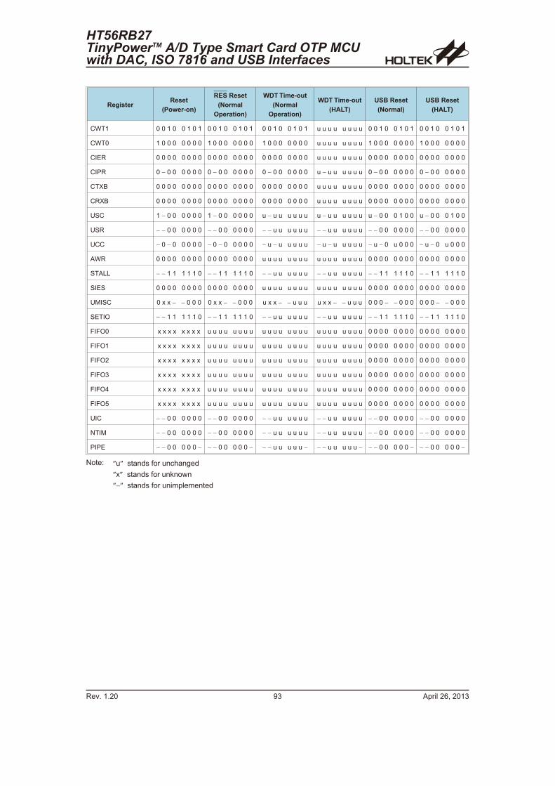
RegisterReset
(Power-on)
RES Reset
(Normal
Operation)
WDT Time-out
(Normal
Operation)
WDT Time-out
(HALT)
USB Reset
(Normal)
USB Reset
(HALT)
CWT1 0 0 1 0 0 1 0 1 0 0 1 0 0 1 0 1 0 0 1 0 0 1 0 1 u u u u u u u u 0 0 1 0 0 1 0 1 0 0 1 0 0 1 0 1
CWT0 1 0 0 0 0 0 0 0 1 0 0 0 0 0 0 0 1 0 0 0 0 0 0 0 u u u u u u u u 1 0 0 0 0 0 0 0 1 0 0 0 0 0 0 0
CIER 0 0 0 0 0 0 0 0 0 0 0 0 0 0 0 0 0 0 0 0 0 0 0 0 u u u u u u u u 0 0 0 0 0 0 0 0 0 0 0 0 0 0 0 0
CIPR 0 � 0 0 0 0 0 0 0 � 0 0 0 0 0 0 0 � 0 0 0 0 0 0 u � u u u u u u 0 � 0 0 0 0 0 0 0 � 0 0 0 0 0 0
CTXB 0 0 0 0 0 0 0 0 0 0 0 0 0 0 0 0 0 0 0 0 0 0 0 0 u u u u u u u u 0 0 0 0 0 0 0 0 0 0 0 0 0 0 0 0
CRXB 0 0 0 0 0 0 0 0 0 0 0 0 0 0 0 0 0 0 0 0 0 0 0 0 u u u u u u u u 0 0 0 0 0 0 0 0 0 0 0 0 0 0 0 0
USC 1 � 0 0 0 0 0 0 1 � 0 0 0 0 0 0 u � u u u u u u u � u u u u u u u � 0 0 0 1 0 0 u � 0 0 0 1 0 0
USR � � 0 0 0 0 0 0 � � 0 0 0 0 0 0 � � u u u u u u � � u u u u u u � � 0 0 0 0 0 0 � � 0 0 0 0 0 0
UCC � 0 � 0 0 0 0 0 � 0 � 0 0 0 0 0 � u � u u u u u � u � u u u u u � u � 0 u 0 0 0 � u � 0 u 0 0 0
AWR 0 0 0 0 0 0 0 0 0 0 0 0 0 0 0 0 u u u u u u u u u u u u u u u u 0 0 0 0 0 0 0 0 0 0 0 0 0 0 0 0
STALL � � 1 1 1 1 1 0 � � 1 1 1 1 1 0 � � u u u u u u � � u u u u u u � � 1 1 1 1 1 0 � � 1 1 1 1 1 0
SIES 0 0 0 0 0 0 0 0 0 0 0 0 0 0 0 0 u u u u u u u u u u u u u u u u 0 0 0 0 0 0 0 0 0 0 0 0 0 0 0 0
UMISC 0 x x � � 0 0 0 0 x x � � 0 0 0 u x x � � u u u u x x � � u u u 0 0 0 � � 0 0 0 0 0 0 � � 0 0 0
SETIO � � 1 1 1 1 1 0 � � 1 1 1 1 1 0 � � u u u u u u � � u u u u u u � � 1 1 1 1 1 0 � � 1 1 1 1 1 0
FIFO0 x x x x x x x x u u u u u u u u u u u u u u u u u u u u u u u u 0 0 0 0 0 0 0 0 0 0 0 0 0 0 0 0
FIFO1 x x x x x x x x u u u u u u u u u u u u u u u u u u u u u u u u 0 0 0 0 0 0 0 0 0 0 0 0 0 0 0 0
FIFO2 x x x x x x x x u u u u u u u u u u u u u u u u u u u u u u u u 0 0 0 0 0 0 0 0 0 0 0 0 0 0 0 0
FIFO3 x x x x x x x x u u u u u u u u u u u u u u u u u u u u u u u u 0 0 0 0 0 0 0 0 0 0 0 0 0 0 0 0
FIFO4 x x x x x x x x u u u u u u u u u u u u u u u u u u u u u u u u 0 0 0 0 0 0 0 0 0 0 0 0 0 0 0 0
FIFO5 x x x x x x x x u u u u u u u u u u u u u u u u u u u u u u u u 0 0 0 0 0 0 0 0 0 0 0 0 0 0 0 0
UIC � � 0 0 0 0 0 0 � � 0 0 0 0 0 0 � � u u u u u u � � u u u u u u � � 0 0 0 0 0 0 � � 0 0 0 0 0 0
NTIM � � 0 0 0 0 0 0 � � 0 0 0 0 0 0 � � u u u u u u � � u u u u u u � � 0 0 0 0 0 0 � � 0 0 0 0 0 0
PIPE � � 0 0 0 0 0 � � � 0 0 0 0 0 � � � u u u u u � � � u u u u u � � � 0 0 0 0 0 � � � 0 0 0 0 0 �
Note: �u� stands for unchanged
�x� stands for unknown
��� stands for unimplemented
HT56RB27TinyPowerTM A/D Type Smart Card OTP MCUwith DAC, ISO 7816 and USB Interfaces
Rev. 1.20 93 April 26, 2013
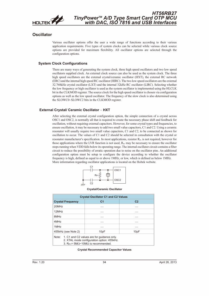
Oscillator
Various oscillator options offer the user a wide range of functions according to their various
application requirements. Five types of system clocks can be selected while various clock source
options are provided for maximum flexibility. All oscillator options are selected through the
configuration options.
System Clock Configurations
There are many ways of generating the system clock, three high speed oscillators and two low speed
oscillators supplied clock. An external clock source can also be used as the system clock. The three
high speed oscillators are the external crystal/ceramic oscillator (HXT), the external RC network
(ERC) and the internal high speed RC oscillator (HIRC). The two low speed oscillators are the external
32.768kHz crystal oscillator (LXT) and the internal 32kHz RC oscillator (LIRC). Selecting whether
the low frequency or high oscillator is used as the system oscillator is implemented using the HLCLK
bit in the CLKMOD register. The source clock for the high speed oscillator is chosen via configuration
options as well as the low speed oscillator. The frequency of the slow clock is also determined using
the SLOWC0~SLOWC2 bits in the CLKMOD register.
External Crystal/ Ceramic Oscillator � HXT
After selecting the external crystal configuration option, the simple connection of a crystal across
OSC1 and OSC2, is normally all that is required to create the necessary phase shift and feedback for
oscillation, without requiring external capacitors. However, for some crystal types and frequencies, to
ensure oscillation, it may be necessary to add two small value capacitors, C1 and C2. Using a ceramic
resonator will usually require two small value capacitors, C1 and C2, to be connected as shown for
oscillation to occur. The values of C1 and C2 should be selected in consultation with the crystal or
resonator manufacturer�s specification. In most applications, resistor RP1 is not required, however for
those applications where the LVR function is not used, RP1 may be necessary to ensure the oscillator
stops running when VDD falls below its operating range. The internal oscillator circuit contains a filter
circuit to reduce the possibility of erratic operation due to noise on the oscillator pins. An additional
configuration option must be setup to configure the device according to whether the oscillator
frequency is high, defined as equal to or above 1MHz, or low, which is defined as below 1MHz.
More information regarding oscillator applications is located on the Holtek website.
Crystal Oscillator C1 and C2 Values
Crystal Frequency C1 C2
20MHz � �
12MHz � �
8MHz � �
4MHz � �
1MHz � �
455kHz (see Note 2) 10pF 10pF
Note: 1. C1 and C2 values are for guidance only.2. XTAL mode configuration option: 455kHz.3. RP1= 5M~10M is recommended.
Crystal Recommended Capacitor Values
Rev. 1.20 94 April 26, 2013
HT56RB27TinyPowerTM A/D Type Smart Card OTP MCU
with DAC, ISO 7816 and USB Interfaces
# � �
# � �
� �
� �
� �
Crystal/Ceramic Oscillator
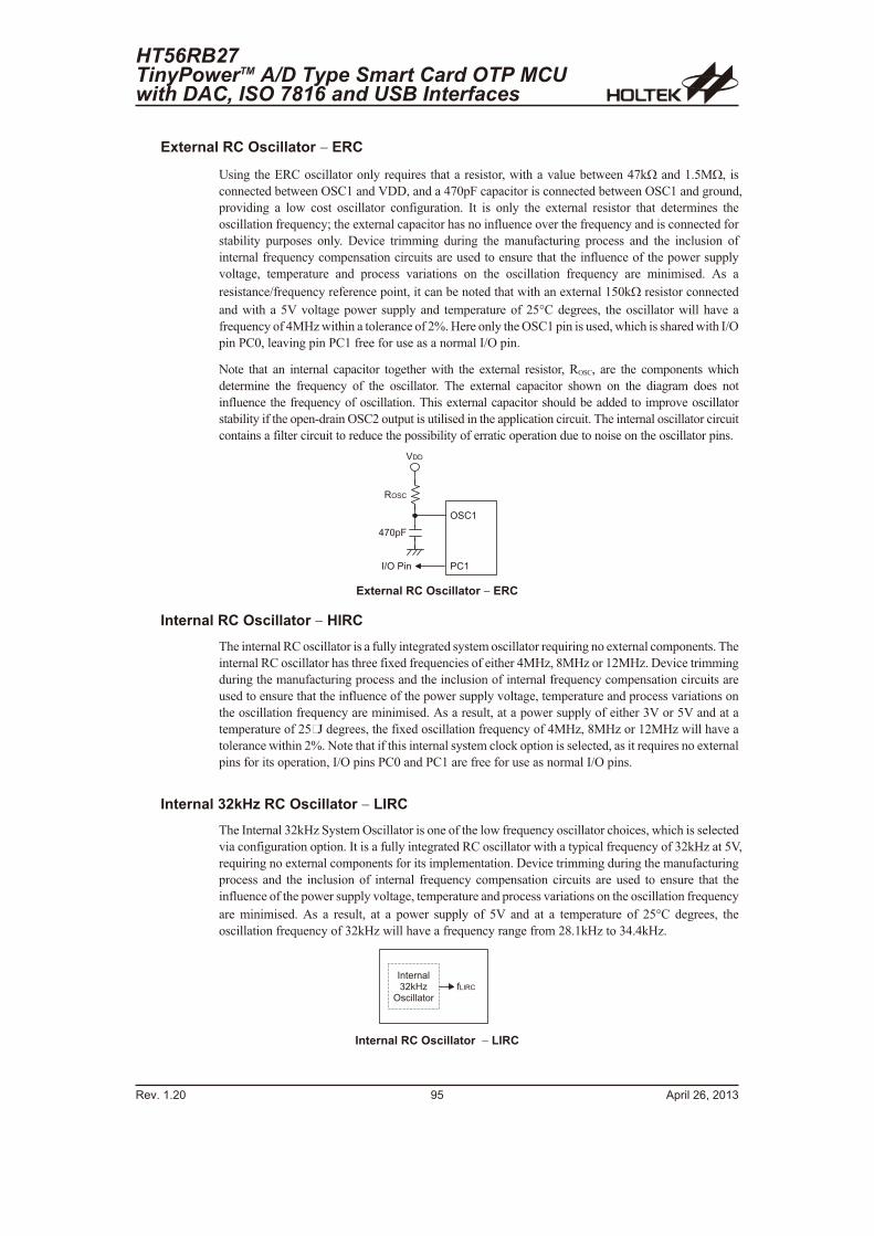
External RC Oscillator � ERC
Using the ERC oscillator only requires that a resistor, with a value between 47k and 1.5M, is
connected between OSC1 and VDD, and a 470pF capacitor is connected between OSC1 and ground,
providing a low cost oscillator configuration. It is only the external resistor that determines the
oscillation frequency; the external capacitor has no influence over the frequency and is connected for
stability purposes only. Device trimming during the manufacturing process and the inclusion of
internal frequency compensation circuits are used to ensure that the influence of the power supply
voltage, temperature and process variations on the oscillation frequency are minimised. As a
resistance/frequency reference point, it can be noted that with an external 150k resistor connected
and with a 5V voltage power supply and temperature of 25C degrees, the oscillator will have a
frequency of 4MHz within a tolerance of 2%. Here only the OSC1 pin is used, which is shared with I/O
pin PC0, leaving pin PC1 free for use as a normal I/O pin.
Note that an internal capacitor together with the external resistor, ROSC, are the components which
determine the frequency of the oscillator. The external capacitor shown on the diagram does not
influence the frequency of oscillation. This external capacitor should be added to improve oscillator
stability if the open-drain OSC2 output is utilised in the application circuit. The internal oscillator circuit
contains a filter circuit to reduce the possibility of erratic operation due to noise on the oscillator pins.
Internal RC Oscillator � HIRC
The internal RC oscillator is a fully integrated system oscillator requiring no external components. The
internal RC oscillator has three fixed frequencies of either 4MHz, 8MHz or 12MHz. Device trimming
during the manufacturing process and the inclusion of internal frequency compensation circuits are
used to ensure that the influence of the power supply voltage, temperature and process variations on
the oscillation frequency are minimised. As a result, at a power supply of either 3V or 5V and at a
temperature of 25¢J degrees, the fixed oscillation frequency of 4MHz, 8MHz or 12MHz will have a
tolerance within 2%. Note that if this internal system clock option is selected, as it requires no external
pins for its operation, I/O pins PC0 and PC1 are free for use as normal I/O pins.
Internal 32kHz RC Oscillator � LIRC
The Internal 32kHz System Oscillator is one of the low frequency oscillator choices, which is selected
via configuration option. It is a fully integrated RC oscillator with a typical frequency of 32kHz at 5V,
requiring no external components for its implementation. Device trimming during the manufacturing
process and the inclusion of internal frequency compensation circuits are used to ensure that the
influence of the power supply voltage, temperature and process variations on the oscillation frequency
are minimised. As a result, at a power supply of 5V and at a temperature of 25C degrees, the
oscillation frequency of 32kHz will have a frequency range from 28.1kHz to 34.4kHz.
HT56RB27TinyPowerTM A/D Type Smart Card OTP MCUwith DAC, ISO 7816 and USB Interfaces
Rev. 1.20 95 April 26, 2013
� � � � ! � � �& � " 2 H
� � � � � � !: + � �
Internal RC Oscillator � LIRC
# � �
� � �� = � � � �
' 5 7 ( �
� � �
# �
External RC Oscillator � ERC
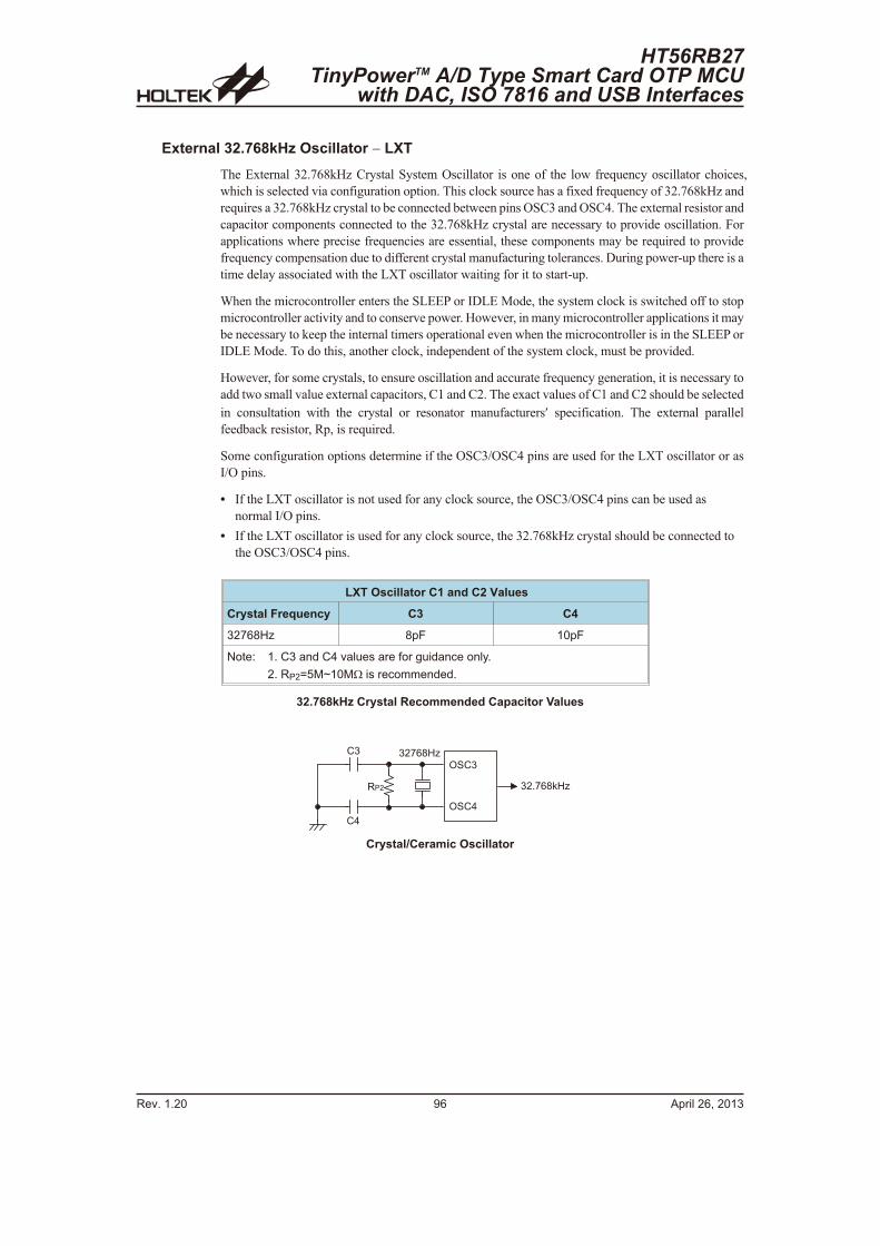
External 32.768kHz Oscillator � LXT
The External 32.768kHz Crystal System Oscillator is one of the low frequency oscillator choices,
which is selected via configuration option. This clock source has a fixed frequency of 32.768kHz and
requires a 32.768kHz crystal to be connected between pins OSC3 and OSC4. The external resistor and
capacitor components connected to the 32.768kHz crystal are necessary to provide oscillation. For
applications where precise frequencies are essential, these components may be required to provide
frequency compensation due to different crystal manufacturing tolerances. During power-up there is a
time delay associated with the LXT oscillator waiting for it to start-up.
When the microcontroller enters the SLEEP or IDLE Mode, the system clock is switched off to stop
microcontroller activity and to conserve power. However, in many microcontroller applications it may
be necessary to keep the internal timers operational even when the microcontroller is in the SLEEP or
IDLE Mode. To do this, another clock, independent of the system clock, must be provided.
However, for some crystals, to ensure oscillation and accurate frequency generation, it is necessary to
add two small value external capacitors, C1 and C2. The exact values of C1 and C2 should be selected
in consultation with the crystal or resonator manufacturers� specification. The external parallel
feedback resistor, Rp, is required.
Some configuration options determine if the OSC3/OSC4 pins are used for the LXT oscillator or as
I/O pins.
� If the LXT oscillator is not used for any clock source, the OSC3/OSC4 pins can be used as
normal I/O pins.
� If the LXT oscillator is used for any clock source, the 32.768kHz crystal should be connected to
the OSC3/OSC4 pins.
LXT Oscillator C1 and C2 Values
Crystal Frequency C3 C4
32768Hz 8pF 10pF
Note: 1. C3 and C4 values are for guidance only.
2. RP2=5M~10M is recommended.
32.768kHz Crystal Recommended Capacitor Values
Rev. 1.20 96 April 26, 2013
HT56RB27TinyPowerTM A/D Type Smart Card OTP MCU
with DAC, ISO 7816 and USB Interfaces
# � '
# � &
� '
� &
� �
& � 5 * 6 2 H
& � � 5 * 6 " 2 H
Crystal/Ceramic Oscillator
LXT Oscillator Low Power Function
The LXT oscillator can function in one of two modes, the Quick Start Mode and the Low Power Mode.
The mode selection is executed using the QOSC bit in the RTCC register.
QOSC Bit LXT Mode
0 Quick Start
1 Low-power
After power on, the QOSC bit will be automatically cleared to zero ensuring that the LXT oscillator is
in the Quick Start operating mode. In the Quick Start Mode the LXT oscillator will power up and
stabilise quickly. However, after the LXT oscillator has fully powered up it can be placed into the
Low-power mode by setting the QOSC bit high. The oscillator will continue to run but with reduced
current consumption, as the higher current consumption is only required during the LXT oscillator
start-up. In power sensitive applications, such as battery applications, where power consumption must
be kept to a minimum, it is therefore recommended that the application program sets the QOSC bit
high about 2 seconds after power-on.
It should be noted that, no matter what condition the QOSC bit is set to, the LXT oscillator will always
function normally, the only difference is that it will take more time to start up if in the Low-power
mode.
External Oscillator � EC
The system clock can also be supplied by an externally supplied clock giving users a method of
synchronizing their external hardware to the microcontroller operation. This is selected using a
configuration option and supplying the clock on pin OSC1. Pin OSC2 can be used as a normal I/O pin
if the external oscillator is used. The internal oscillator circuit contains a filter circuit to reduce the
possibility of erratic operation due to noise on the oscillator pin. However, as the filter circuit
consumes a certain amount of power, an oscillator configuration option exists to turn this filter off. Not
using the internal filter should be considered in power sensitive applications and where the externally
supplied clock is of a high integrity and supplied by a low impedance source.
System Operating Modes
The device has the ability to operate in several different modes. This range of operating modes, known
as Normal Mode, Slow Mode, Idle Mode and Sleep Mode, allow the device to run using a wide range
of different slow and fast clock sources. The devices also possess the ability to dynamically switch
between different clocks and operating modes. With this choice of operating functions users are
provided with the flexibility to ensure they obtain optimal performance from the device according to
their application specific requirements.
Clock Sources
In discussing the system clocks for the device, they can be seen as having a dual clock mode. These
dual clocks are what are known as a High Oscillator and the other as a Low Oscillator. The High and
Low Oscillator are the system clock sources and can be selected dynamically using the HLCLK bit in
the CLKMOD register. The High Oscillator has the internal name fM whose source is selected using a
configuration option from a choice of either an external crystal/resonator, external RC oscillator or
external clock source.
HT56RB27TinyPowerTM A/D Type Smart Card OTP MCUwith DAC, ISO 7816 and USB Interfaces
Rev. 1.20 97 April 26, 2013
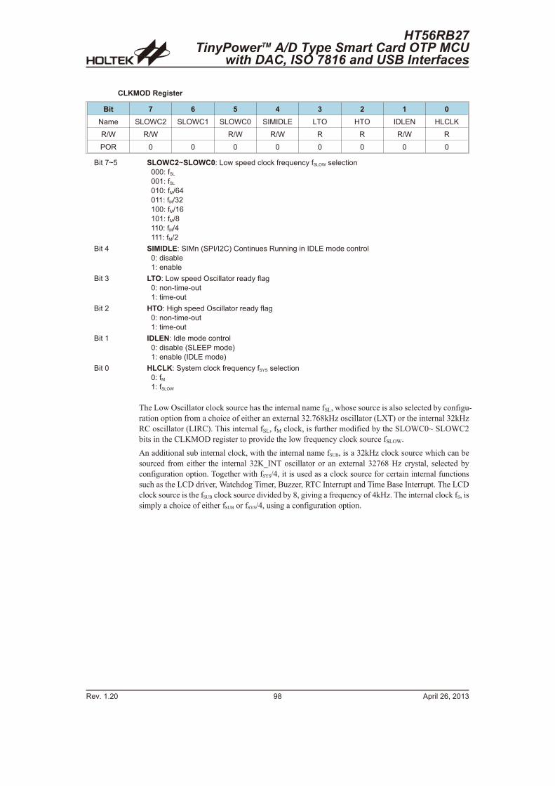
CLKMOD Register
Bit 7 6 5 4 3 2 1 0
Name SLOWC2 SLOWC1 SLOWC0 SIMIDLE LTO HTO IDLEN HLCLK
R/W R/W R/W R/W R R R/W R
POR 0 0 0 0 0 0 0 0
Bit 7~5 SLOWC2~SLOWC0: Low speed clock frequency fSLOW selection
000: fSL
001: fSL
010: fM/64
011: fM/32
100: fM/16
101: fM/8
110: fM/4
111: fM/2
Bit 4 SIMIDLE: SIMn (SPI/I2C) Continues Running in IDLE mode control
0: disable
1: enable
Bit 3 LTO: Low speed Oscillator ready flag
0: non-time-out
1: time-out
Bit 2 HTO: High speed Oscillator ready flag
0: non-time-out
1: time-out
Bit 1 IDLEN: Idle mode control
0: disable (SLEEP mode)
1: enable (IDLE mode)
Bit 0 HLCLK: System clock frequency fSYS selection
0: fM
1: fSLOW
The Low Oscillator clock source has the internal name fSL, whose source is also selected by configu-
ration option from a choice of either an external 32.768kHz oscillator (LXT) or the internal 32kHz
RC oscillator (LIRC). This internal fSL, fM clock, is further modified by the SLOWC0~ SLOWC2
bits in the CLKMOD register to provide the low frequency clock source fSLOW.
An additional sub internal clock, with the internal name fSUB, is a 32kHz clock source which can be
sourced from either the internal 32K_INT oscillator or an external 32768 Hz crystal, selected by
configuration option. Together with fSYS/4, it is used as a clock source for certain internal functions
such as the LCD driver, Watchdog Timer, Buzzer, RTC Interrupt and Time Base Interrupt. The LCD
clock source is the fSUB clock source divided by 8, giving a frequency of 4kHz. The internal clock fS, is
simply a choice of either fSUB or fSYS/4, using a configuration option.
Rev. 1.20 98 April 26, 2013
HT56RB27TinyPowerTM A/D Type Smart Card OTP MCU
with DAC, ISO 7816 and USB Interfaces
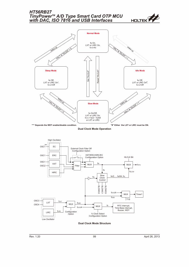
HT56RB27TinyPowerTM A/D Type Smart Card OTP MCUwith DAC, ISO 7816 and USB Interfaces
Rev. 1.20 99 April 26, 2013
� � � � � � � � � �
�
? �" �� �(
2 ,+ �� O� E �� +
� 4E � I� 7
2 , + � � O � E � � + � 4 E � I � �
? � " � � � (
�
? �" �� �(
2 ,+ �� O� E �� +
� 4E � I� �
2 , + � � O � E � � + � 4 E � I � 7
? � " � � � (
#���E2
+�+BE
�����E2
+�+BE
� � � � � � � � � � ! � " � # � � � $ � % � � � � $ � � & � � � � � � � � ' � ( � � ) � � ! � � � � ! � * + # � � � � * � , � � � � � $ � - � '
: / � � 0+ D � � ! � + � � � � 0
: # - # I : /
� � � � � �
: / � : : 0+ D � � ! � + � � � � J 0
: # - # I : :
� � � � � � �
: / � : : 0+ D � � ! � + � � � � � 0
: # - # I : :
� � � . � � � �
: / � � = : : 0+ D � � ! � + � � � � 0: # - # � I � : / = � � G � : / = * ' ! � + D � � ! � + � �
P
Dual Clock Mode Operation
/ > D
: # + C
2 + � + B � 8 � �
: # - #
: /
/ > D
: + D �
: # +# � ?� � "� � � ! �
#+C�7
+ D �
: + � � � � : � % � ! � � � � ( � � �
#+C��
#+C��
: / = � 0 � � � � � : / = * ' 0 � : # +
/ > D
/ > D : #: # - # = '
: # > 8
: # - # = '
: # > 8
� � � � ! �
� � #
: # � � � " � # � � � �� � : � % � ! � � � � � ( � � �
� � � � � � � ! ! � ( � 0� � � � � 8 � � � � � � � � ! ! � ( � 0
8 � H H � ! 0 � C � �+ � �
+ ? � � � � � � � !
# � &
# � '
� �
2 D � / > D: /
2 D � = � � = 2 � � = � �� � : � % � ! � � � � � ( � � �
2 � % � � � � � � � � !
# � �
# � �
# � � � � � � � !
� � � � ! � � � � � � " � � � � � � ! � : :� � : � % � ! � � � � � ( � � �
� � # � �
2 � �
Dual Clock Mode Structure
Operating Modes
After the correct clock source configuration selections are made, overall operation of the chosen clock
is achieved using the CLKMOD register. A combination of the HLCLK and IDLEN bits in the
CLKMOD register and use of the HALT instruction determine in which mode the device will be run.
The devices can operate in the following Modes.
� Normal mode
fM on, fSLOW on, fSYS=fM, CPU on, fS on, fWDT on/off depending upon the WDT configuration option and
WDT control register.
� Slow Mode0
fM off, fSYS=fSLOW, fSLOW=fSL=fLIRC or fLXT, CPU on, fS on, fWDT on/off depending upon the WDT
configuration option and WDT control register.
� Slow Mode1
fM on, fSYS=fSLOW= fM/2~fM/64, CPU on, fS on, fWDT on/off depending upon the WDT configuration
option and WDT control register.
� IDLE mode
fM, fSLOW, fSYS off, CPU off; fSUB on, fS on/off by selecting fSUB or fSYS /4, fWDT on/off depending upon the
WDT configuration option and WDT control register.
The IDLE mode is determined by the IDLE Mode Control bit named IDLEN in the CLKMOD
register when the HALT instruction is executed. If this bit is high, when a HALT instruction is
executed the device will enter the IDLE Mode. If the bit is low the device will enter the SLEEP Mode
when a HALT instruction is executed.
� SLEEP mode
fM, fSLOW, fSYS, fS, CPU off; fSUB, fWDT on/off depending upon the WDT configuration option and WDT
control register.
The SLEEP mode is determined by setting the IDLE Mode Control bit named IDLEN to 0 when the
HALT instruction is executed.
Operation ModeDescription
CPU fSYS fSUB fS fLCD
Normal Mode On fM On On On/Off (4)
Slow 0 Mode On fSLOW=fLIRC or fLXT On On On/Off (4)
Slow 1 Mode On fSLOW=fM/2~fM/64 On On On/Off (4)
IDLE Mode On On/Off (1) On On/Off (3) On/Off (4)
SLEEP Mode On Off On/Off (2) On/Off (3) Off
Note: 1. In the IDLE Mode, the fSYS clock on/off function is determined by whether the SIMIDLE bit set to 1 or 0
respectively and can only be used for the master SPI operation or PCLK output for which the clock source
comes from the fSYS clock.
2. In the SLEEP mode the fSUB clock on/off function is determined by whether the WDT is enabled or disabled
respectively.
3. The fS clock on/off function in the IDLE or SLEEP mode is determined by whether the selected clock source
of the WDT function is fSUB or the fSYS/4 clock.
4. The fLCD clock turned on/off function is determined by the LCDEN or LEDEN control bit.
Rev. 1.20 100 April 26, 2013
HT56RB27TinyPowerTM A/D Type Smart Card OTP MCU
with DAC, ISO 7816 and USB Interfaces
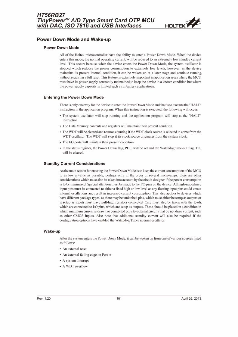
Power Down Mode and Wake-up
Power Down Mode
All of the Holtek microcontroller have the ability to enter a Power Down Mode. When the device
enters this mode, the normal operating current, will be reduced to an extremely low standby current
level. This occurs because when the device enters the Power Down Mode, the system oscillator is
stopped which reduces the power consumption to extremely low levels, however, as the device
maintains its present internal condition, it can be woken up at a later stage and continue running,
without requiring a full reset. This feature is extremely important in application areas where the MCU
must have its power supply constantly maintained to keep the device in a known condition but where
the power supply capacity is limited such as in battery applications.
Entering the Power Down Mode
There is only one way for the device to enter the Power Down Mode and that is to execute the �HALT�
instruction in the application program. When this instruction is executed, the following will occur:
� The system oscillator will stop running and the application program will stop at the �HALT�
instruction.
� The Data Memory contents and registers will maintain their present condition.
� The WDT will be cleared and resume counting if the WDT clock source is selected to come from the
WDT oscillator. The WDT will stop if its clock source originates from the system clock.
� The I/O ports will maintain their present condition.
� In the status register, the Power Down flag, PDF, will be set and the Watchdog time-out flag, TO,
will be cleared.
Standby Current Considerations
As the main reason for entering the Power Down Mode is to keep the current consumption of the MCU
to as low a value as possible, perhaps only in the order of several micro-amps, there are other
considerations which must also be taken into account by the circuit designer if the power consumption
is to be minimized. Special attention must be made to the I/O pins on the device. All high-impedance
input pins must be connected to either a fixed high or low level as any floating input pins could create
internal oscillations and result in increased current consumption. This also applies to devices which
have different package types, as there may be undonbed pins, which must either be setup as outputs or
if setup as inputs must have pull-high resistors connected. Care must also be taken with the loads,
which are connected to I/O pins, which are setup as outputs. These should be placed in a condition in
which minimum current is drawn or connected only to external circuits that do not draw current, such
as other CMOS inputs. Also note that additional standby current will also be required if the
configuration options have enabled the Watchdog Timer internal oscillator.
Wake-up
After the system enters the Power Down Mode, it can be woken up from one of various sources listed
as follows:
� An external reset
� An external falling edge on Port A
� A system interrupt
� A WDT overflow
HT56RB27TinyPowerTM A/D Type Smart Card OTP MCUwith DAC, ISO 7816 and USB Interfaces
Rev. 1.20 101 April 26, 2013
If the system is woken up by an external reset, the device will experience a full system reset, however,
if the device is woken up by a WDT overflow, a Watchdog Timer reset will be initiated. Although both
of these wake-up methods will initiate a reset operation, the actual source of the wake-up can be
determined by examining the TO and PDF flags. The PDF flag is cleared by a system power-up or
executing the clear Watchdog Timer instructions and is set when executing the �HALT� instruction.
The TO flag is set if a WDT time-out occurs, and causes a wake-up that only resets the Program
Counter and Stack Pointer, the other flags remain in their original status.
Each pin on Port A can be setup via an individual configuration option to permit a negative transition
on the pin to wake-up the system. When a Port A pin wake-up occurs, the program will resume
execution at the instruction following the �HALT� instruction.
If the system is woken up by an interrupt, then two possible situations may occur. The first is where the
related interrupt is disabled or the interrupt is enabled but the stack is full, in which case the program
will resume execution at the instruction following the �HALT� instruction. In this situation, the
interrupt which woke-up the device will not be immediately serviced, but will rather be serviced later
when the related interrupt is finally enabled or when a stack level becomes free. The other situation is
where the related interrupt is enabled and the stack is not full, in which case the regular interrupt
response takes place. If an interrupt request flag is set to �1� before entering the Power Down Mode,
the wake-up function of the related interrupt will be disabled.
No matter what the source of the wake-up event is, once a wake-up situation occurs, a time period
equal to 1024 system clock periods will be required before normal system operation resumes.
However, if the wake-up has originated due to an interrupt, the actual interrupt subroutine execution
will be delayed by an additional one or more cycles. If the wake-up results in the execution of the next
instruction following the �HALT� instruction, this will be executed immediately after the 1024 system
clock period delay has ended.
Low Voltage Detector � LVD
The Low Voltage Detect internal function provides a means for the user to monitor when the power
supply voltage falls below a certain fixed level as specified in the DC characteristics.
LVD Operation
The LVD function must be first enabled via a configuration option after which bits 3 and 5 of the
RTCC register are used to control the overall function of the LVD. Bit 3 is the enable/disable control
bit and is known as LVDC, when set low the overall function of the LVD will be disabled. Bit 5 is the
LVD detector output bit and is known as LVDO. Under normal operation, and when the power supply
voltage is above the specified VLVD value in the DC characteristic section, the LVDO bit will remain
at a zero value. If the power supply voltage should fall below this VLVD value then the LVDO bit will
change to a high value indicating a low voltage condition. Note that the LVDO bit is a read-only bit. By
polling the LVDO bit in the RTCC register, the application program can therefore determine the
presence of a low voltage condition.
After power-on, or after a reset, the LVD will be switched off by clearing the LVDC bit in the RTCC
register to zero. Note that if the LVD is enabled there will be some power consumption associated with
its internal circuitry, however, by clearing the LVDC bit to zero the power can be minimised. It is
important not to confuse the LVD with the LVR function. In the LVR function an automatic reset will
be generated by themicrocontroller, whereas in the LVD function only the LVDO bit will be affected
with no influence on other microcontroller functions.
There are a range of voltage values, selected using a configuration option, which can be chosen to
activate the LVD.
Rev. 1.20 102 April 26, 2013
HT56RB27TinyPowerTM A/D Type Smart Card OTP MCU
with DAC, ISO 7816 and USB Interfaces
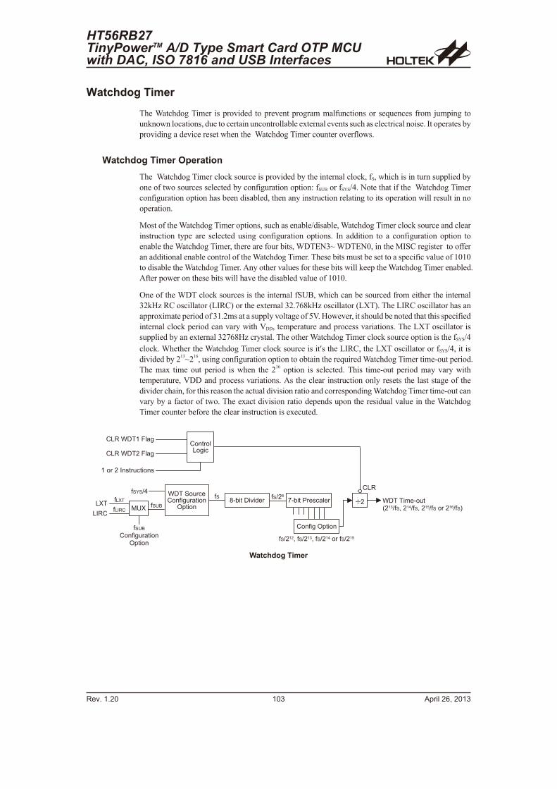
Watchdog Timer
The Watchdog Timer is provided to prevent program malfunctions or sequences from jumping to
unknown locations, due to certain uncontrollable external events such as electrical noise. It operates by
providing a device reset when the Watchdog Timer counter overflows.
Watchdog Timer Operation
The Watchdog Timer clock source is provided by the internal clock, fS, which is in turn supplied by
one of two sources selected by configuration option: fSUB or fSYS/4. Note that if the Watchdog Timer
configuration option has been disabled, then any instruction relating to its operation will result in no
operation.
Most of the Watchdog Timer options, such as enable/disable, Watchdog Timer clock source and clear
instruction type are selected using configuration options. In addition to a configuration option to
enable the Watchdog Timer, there are four bits, WDTEN3~ WDTEN0, in the MISC register to offer
an additional enable control of the Watchdog Timer. These bits must be set to a specific value of 1010
to disable the Watchdog Timer. Any other values for these bits will keep the Watchdog Timer enabled.
After power on these bits will have the disabled value of 1010.
One of the WDT clock sources is the internal fSUB, which can be sourced from either the internal
32kHz RC oscillator (LIRC) or the external 32.768kHz oscillator (LXT). The LIRC oscillator has an
approximate period of 31.2ms at a supply voltage of 5V. However, it should be noted that this specified
internal clock period can vary with VDD, temperature and process variations. The LXT oscillator is
supplied by an external 32768Hz crystal. The other Watchdog Timer clock source option is the fSYS/4
clock. Whether the Watchdog Timer clock source is it�s the LIRC, the LXT oscillator or fSYS/4, it is
divided by 213
~216
, using configuration option to obtain the required Watchdog Timer time-out period.
The max time out period is when the 216
option is selected. This time-out period may vary with
temperature, VDD and process variations. As the clear instruction only resets the last stage of the
divider chain, for this reason the actual division ratio and corresponding Watchdog Timer time-out can
vary by a factor of two. The exact division ratio depends upon the residual value in the Watchdog
Timer counter before the clear instruction is executed.
HT56RB27TinyPowerTM A/D Type Smart Card OTP MCUwith DAC, ISO 7816 and USB Interfaces
Rev. 1.20 103 April 26, 2013
C � � � # � ! �� � : � % � ! � � � �
( � � �
� � � ! �+ % �
� + � C � � � � � � � %
� + � C � � � � � � � %
� � ! � � � � � � � ! � � � � �
6 � < � � � � � 9 � ; � !: #
� + �
C � � � � � � � � � �� � � & = : # 0 � � � ' = : # 0 � � � ) = : # � ! � � � * = : # �
� �5 � < � � � � ! � � � � � !: # = � 6
: # = � � � 0 � : # = � � & 0 � : # = � � ' � ! � : # = � � )
� � : � % � ( � � �
+ D �
+ � �
: + D �
: + � �
: # - # = '
: # > 8/ > D
: # > 8� � : � % � ! � � � �
( � � �
Watchdog Timer
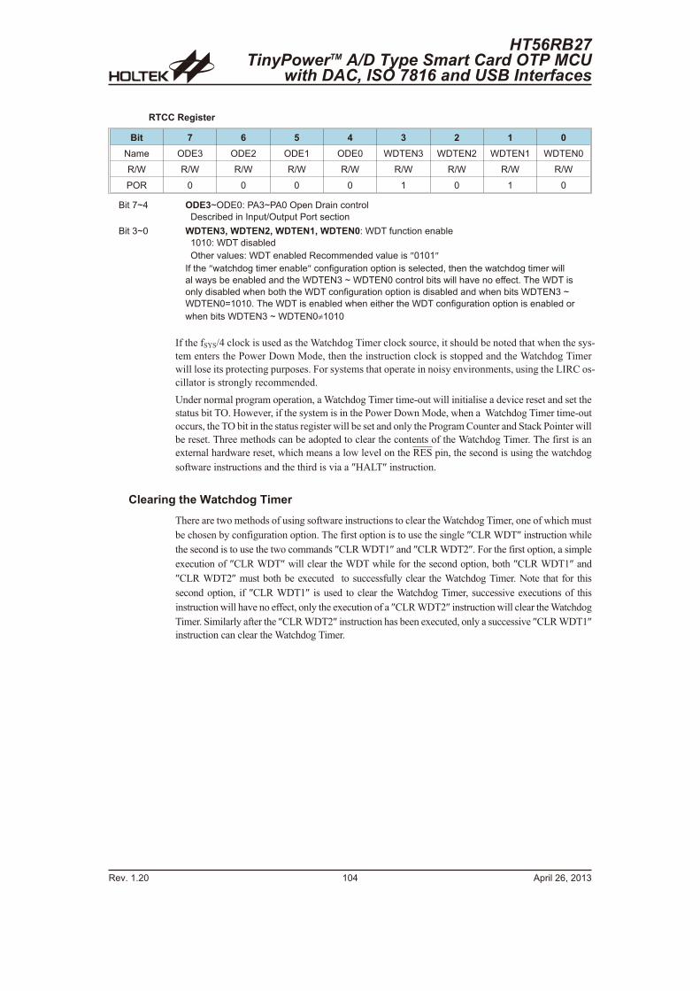
RTCC Register
Bit 7 6 5 4 3 2 1 0
Name ODE3 ODE2 ODE1 ODE0 WDTEN3 WDTEN2 WDTEN1 WDTEN0
R/W R/W R/W R/W R/W R/W R/W R/W R/W
POR 0 0 0 0 1 0 1 0
Bit 7~4 ODE3~ODE0: PA3~PA0 Open Drain control
Described in Input/Output Port section
Bit 3~0 WDTEN3, WDTEN2, WDTEN1, WDTEN0: WDT function enable
1010: WDT disabled
Other values: WDT enabled Recommended value is �0101�
If the �watchdog timer enable� configuration option is selected, then the watchdog timer will
al ways be enabled and the WDTEN3 ~ WDTEN0 control bits will have no effect. The WDT is
only disabled when both the WDT configuration option is disabled and when bits WDTEN3 ~
WDTEN0=1010. The WDT is enabled when either the WDT configuration option is enabled or
when bits WDTEN3 ~ WDTEN0�1010
If the fSYS/4 clock is used as the Watchdog Timer clock source, it should be noted that when the sys-
tem enters the Power Down Mode, then the instruction clock is stopped and the Watchdog Timer
will lose its protecting purposes. For systems that operate in noisy environments, using the LIRC os-
cillator is strongly recommended.
Under normal program operation, a Watchdog Timer time-out will initialise a device reset and set the
status bit TO. However, if the system is in the Power Down Mode, when a Watchdog Timer time-out
occurs, the TO bit in the status register will be set and only the Program Counter and Stack Pointer will
be reset. Three methods can be adopted to clear the contents of the Watchdog Timer. The first is an
external hardware reset, which means a low level on the RES pin, the second is using the watchdog
software instructions and the third is via a �HALT� instruction.
Clearing the Watchdog Timer
There are two methods of using software instructions to clear the Watchdog Timer, one of which must
be chosen by configuration option. The first option is to use the single �CLR WDT� instruction while
the second is to use the two commands �CLR WDT1� and �CLR WDT2�. For the first option, a simple
execution of �CLR WDT� will clear the WDT while for the second option, both �CLR WDT1� and
�CLR WDT2� must both be executed to successfully clear the Watchdog Timer. Note that for this
second option, if �CLR WDT1� is used to clear the Watchdog Timer, successive executions of this
instruction will have no effect, only the execution of a �CLR WDT2� instruction will clear the Watchdog
Timer. Similarly after the �CLR WDT2� instruction has been executed, only a successive �CLR WDT1�
instruction can clear the Watchdog Timer.
Rev. 1.20 104 April 26, 2013
HT56RB27TinyPowerTM A/D Type Smart Card OTP MCU
with DAC, ISO 7816 and USB Interfaces
USB Interface
The devices contains an embedded USB Module, which is a 4-wire serial bus that allows
communication with an external host device. Atoken based protocol method is used by the host device
for communication control. Other advantages of the USB bus include live plugging and unplugging
and dynamic device configuration. It is particularly suitable for the devices with data links between
PCs or peripheral devices, or the devices with USB interface such as USB mice, USB keyboards or
USB joysticks, etc.
As the complexity of USB data protocol does not permit comprehensive USB operation information to
be provided in this datasheet, the reader should therefore consult other external information for a
detailed USB understanding.
USB Operation
To communicate with an external USB host, the internal USB module has external pins known as DP
and DM along with the 3.3V regulator output V33O. The USB module has 6 endpoints and a 160 byte
FIFO for the endpoints respectively. A Serial Interface Engine (SIE) decodes the incoming USB data
stream and transfers it to the correct endpoint buffer memory (FIFO). A series of status registers
provide the user with the USB data transfer situation as well as any error conditions. The USB contains
its own independent interrupt which can be used to indicate when the USB FIFOs are accessed by the
host device or a change of the USB operating conditions including the USB suspend mode, resume
event or USB reset occurs.
USB Status and Control Registers
There are several registers associated with the USB function. Some of the registers control the overall
function of the USB module as well as the interrupts, while some of the registers contain the status bits
which indicate the USB data transfer situations and error condition. Also there are FIFOs for the USB
endpoints to store the data received from or to be transmitted to the USB host. The USB module has 6
endpoints (EP0~EP5) with a different FIFO size for each one. The FIFO size is 8 bytes for EP0~EP2
and EP4 which support �Interrupt transfer�, while the FIFO size for EP3 and EP5 is 64 bytes which can
support �Bulk transfer�.
HT56RB27TinyPowerTM A/D Type Smart Card OTP MCUwith DAC, ISO 7816 and USB Interfaces
Rev. 1.20 105 April 26, 2013
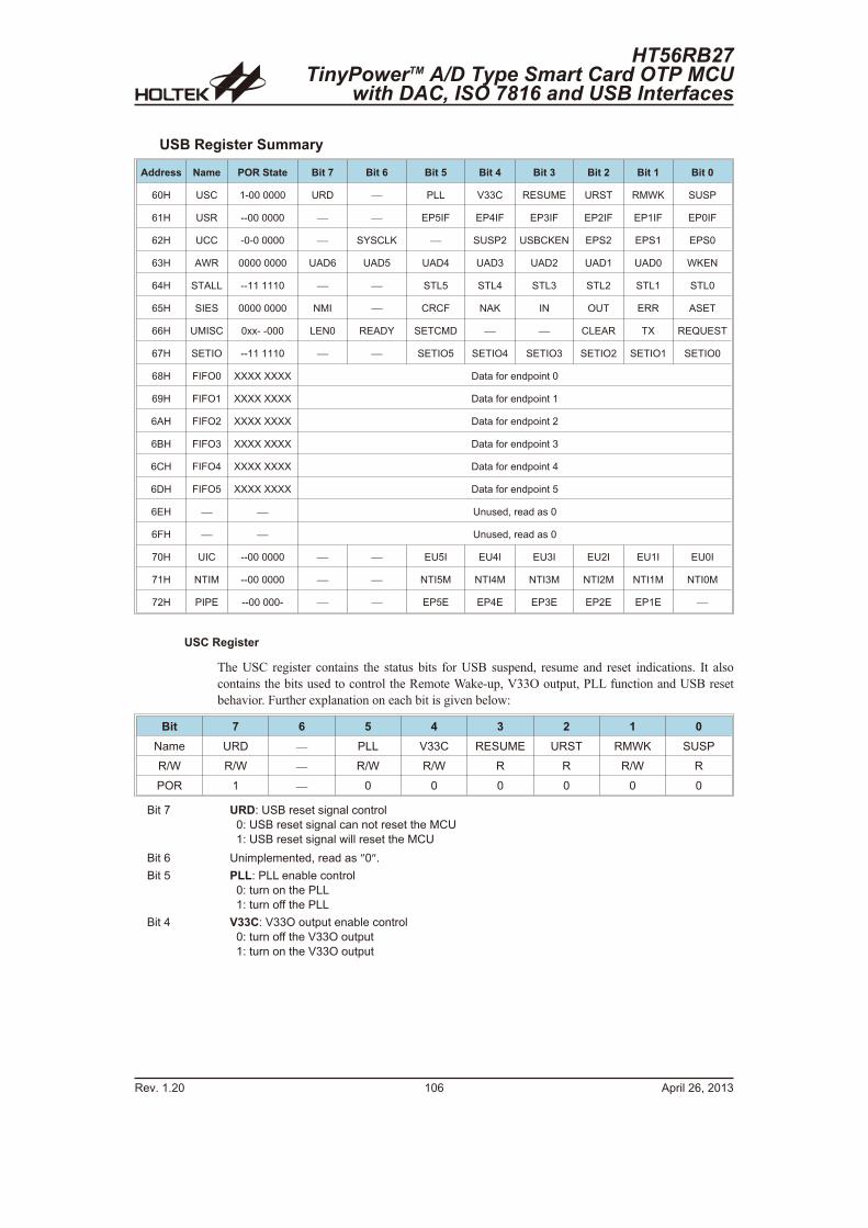
USB Register Summary
Address Name POR State Bit 7 Bit 6 Bit 5 Bit 4 Bit 3 Bit 2 Bit 1 Bit 0
60H USC 1-00 0000 URD � PLL V33C RESUME URST RMWK SUSP
61H USR --00 0000 � � EP5IF EP4IF EP3IF EP2IF EP1IF EP0IF
62H UCC -0-0 0000 � SYSCLK � SUSP2 USBCKEN EPS2 EPS1 EPS0
63H AWR 0000 0000 UAD6 UAD5 UAD4 UAD3 UAD2 UAD1 UAD0 WKEN
64H STALL --11 1110 � � STL5 STL4 STL3 STL2 STL1 STL0
65H SIES 0000 0000 NMI � CRCF NAK IN OUT ERR ASET
66H UMISC 0xx- -000 LEN0 READY SETCMD � � CLEAR TX REQUEST
67H SETIO --11 1110 � � SETIO5 SETIO4 SETIO3 SETIO2 SETIO1 SETIO0
68H FIFO0 XXXX XXXX Data for endpoint 0
69H FIFO1 XXXX XXXX Data for endpoint 1
6AH FIFO2 XXXX XXXX Data for endpoint 2
6BH FIFO3 XXXX XXXX Data for endpoint 3
6CH FIFO4 XXXX XXXX Data for endpoint 4
6DH FIFO5 XXXX XXXX Data for endpoint 5
6EH � � Unused, read as 0
6FH � � Unused, read as 0
70H UIC --00 0000 � � EU5I EU4I EU3I EU2I EU1I EU0I
71H NTIM --00 0000 � � NTI5M NTI4M NTI3M NTI2M NTI1M NTI0M
72H PIPE --00 000- � � EP5E EP4E EP3E EP2E EP1E �
USC Register
The USC register contains the status bits for USB suspend, resume and reset indications. It also
contains the bits used to control the Remote Wake-up, V33O output, PLL function and USB reset
behavior. Further explanation on each bit is given below:
Bit 7 6 5 4 3 2 1 0
Name URD � PLL V33C RESUME URST RMWK SUSP
R/W R/W � R/W R/W R R R/W R
POR 1 � 0 0 0 0 0 0
Bit 7 URD: USB reset signal control
0: USB reset signal can not reset the MCU
1: USB reset signal will reset the MCU
Bit 6 Unimplemented, read as �0�.
Bit 5 PLL: PLL enable control
0: turn on the PLL
1: turn off the PLL
Bit 4 V33C: V33O output enable control
0: turn off the V33O output
1: turn on the V33O output
Rev. 1.20 106 April 26, 2013
HT56RB27TinyPowerTM A/D Type Smart Card OTP MCU
with DAC, ISO 7816 and USB Interfaces
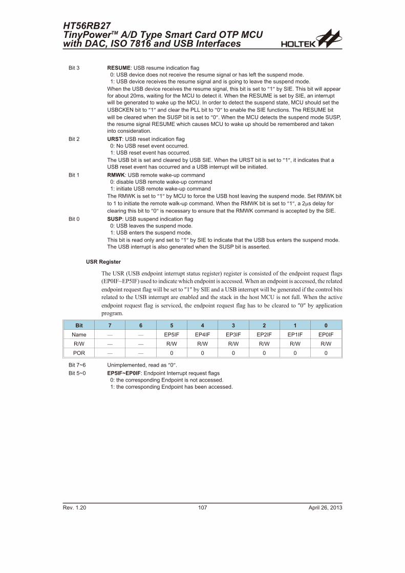
Bit 3 RESUME: USB resume indication flag
0: USB device does not receive the resume signal or has left the suspend mode.
1: USB device receives the resume signal and is going to leave the suspend mode.
When the USB device receives the resume signal, this bit is set to �1� by SIE. This bit will appear
for about 20ms, waiting for the MCU to detect it. When the RESUME is set by SIE, an interrupt
will be generated to wake up the MCU. In order to detect the suspend state, MCU should set the
USBCKEN bit to �1� and clear the PLL bit to �0� to enable the SIE functions. The RESUME bit
will be cleared when the SUSP bit is set to �0�. When the MCU detects the suspend mode SUSP,
the resume signal RESUME which causes MCU to wake up should be remembered and taken
into consideration.
Bit 2 URST: USB reset indication flag
0: No USB reset event occurred.
1: USB reset event has occurred.
The USB bit is set and cleared by USB SIE. When the URST bit is set to �1�, it indicates that a
USB reset event has occurred and a USB interrupt will be initiated.
Bit 1 RMWK: USB remote wake-up command
0: disable USB remote wake-up command
1: initiate USB remote wake-up command
The RMWK is set to �1� by MCU to force the USB host leaving the suspend mode. Set RMWK bit
to 1 to initiate the remote walk-up command. When the RMWK bit is set to �1�, a 2�s delay for
clearing this bit to �0� is necessary to ensure that the RMWK command is accepted by the SIE.
Bit 0 SUSP: USB suspend indication flag
0: USB leaves the suspend mode.
1: USB enters the suspend mode.
This bit is read only and set to �1� by SIE to indicate that the USB bus enters the suspend mode.
The USB interrupt is also generated when the SUSP bit is asserted.
USR Register
The USR (USB endpoint interrupt status register) register is consisted of the endpoint request flags
(EP0IF~EP5IF) used to indicate which endpoint is accessed. When an endpoint is accessed, the related
endpoint request flag will be set to �1� by SIE and a USB interrupt will be generated if the control bits
related to the USB interrupt are enabled and the stack in the host MCU is not full. When the active
endpoint request flag is serviced, the endpoint request flag has to be cleared to �0� by application
program.
Bit 7 6 5 4 3 2 1 0
Name � � EP5IF EP4IF EP3IF EP2IF EP1IF EP0IF
R/W � � R/W R/W R/W R/W R/W R/W
POR � � 0 0 0 0 0 0
Bit 7~6 Unimplemented, read as �0�.
Bit 5~0 EP5IF~EP0IF: Endpoint Interrupt request flags
0: the corresponding Endpoint is not accessed.
1: the corresponding Endpoint has been accessed.
HT56RB27TinyPowerTM A/D Type Smart Card OTP MCUwith DAC, ISO 7816 and USB Interfaces
Rev. 1.20 107 April 26, 2013
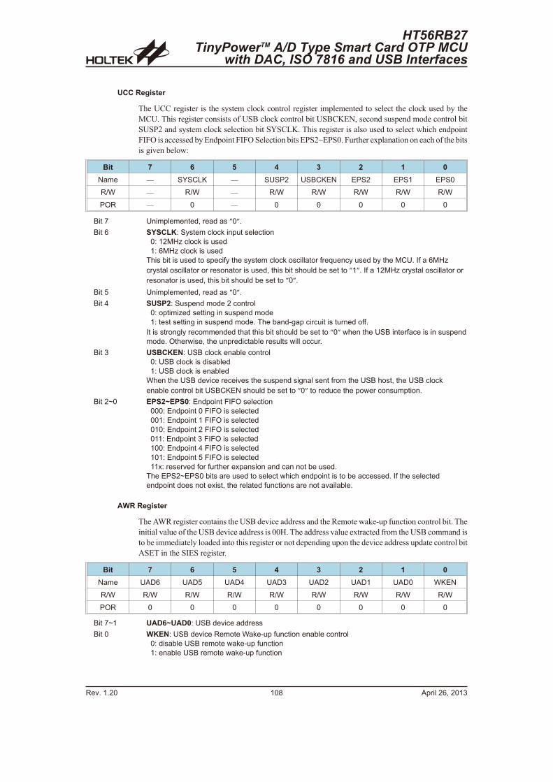
UCC Register
The UCC register is the system clock control register implemented to select the clock used by the
MCU. This register consists of USB clock control bit USBCKEN, second suspend mode control bit
SUSP2 and system clock selection bit SYSCLK. This register is also used to select which endpoint
FIFO is accessed by Endpoint FIFO Selection bits EPS2~EPS0. Further explanation on each of the bits
is given below:
Bit 7 6 5 4 3 2 1 0
Name � SYSCLK � SUSP2 USBCKEN EPS2 EPS1 EPS0
R/W � R/W � R/W R/W R/W R/W R/W
POR � 0 � 0 0 0 0 0
Bit 7 Unimplemented, read as �0�.
Bit 6 SYSCLK: System clock input selection
0: 12MHz clock is used
1: 6MHz clock is used
This bit is used to specify the system clock oscillator frequency used by the MCU. If a 6MHz
crystal oscillator or resonator is used, this bit should be set to �1�. If a 12MHz crystal oscillator or
resonator is used, this bit should be set to �0�.
Bit 5 Unimplemented, read as �0�.
Bit 4 SUSP2: Suspend mode 2 control
0: optimized setting in suspend mode
1: test setting in suspend mode. The band-gap circuit is turned off.
It is strongly recommended that this bit should be set to �0� when the USB interface is in suspend
mode. Otherwise, the unpredictable results will occur.
Bit 3 USBCKEN: USB clock enable control
0: USB clock is disabled
1: USB clock is enabled
When the USB device receives the suspend signal sent from the USB host, the USB clock
enable control bit USBCKEN should be set to �0� to reduce the power consumption.
Bit 2~0 EPS2~EPS0: Endpoint FIFO selection
000: Endpoint 0 FIFO is selected
001: Endpoint 1 FIFO is selected
010: Endpoint 2 FIFO is selected
011: Endpoint 3 FIFO is selected
100: Endpoint 4 FIFO is selected
101: Endpoint 5 FIFO is selected
11x: reserved for further expansion and can not be used.
The EPS2~EPS0 bits are used to select which endpoint is to be accessed. If the selected
endpoint does not exist, the related functions are not available.
AWR Register
The AWR register contains the USB device address and the Remote wake-up function control bit. The
initial value of the USB device address is 00H. The address value extracted from the USB command is
to be immediately loaded into this register or not depending upon the device address update control bit
ASET in the SIES register.
Bit 7 6 5 4 3 2 1 0
Name UAD6 UAD5 UAD4 UAD3 UAD2 UAD1 UAD0 WKEN
R/W R/W R/W R/W R/W R/W R/W R/W R/W
POR 0 0 0 0 0 0 0 0
Bit 7~1 UAD6~UAD0: USB device address
Bit 0 WKEN: USB device Remote Wake-up function enable control
0: disable USB remote wake-up function
1: enable USB remote wake-up function
Rev. 1.20 108 April 26, 2013
HT56RB27TinyPowerTM A/D Type Smart Card OTP MCU
with DAC, ISO 7816 and USB Interfaces
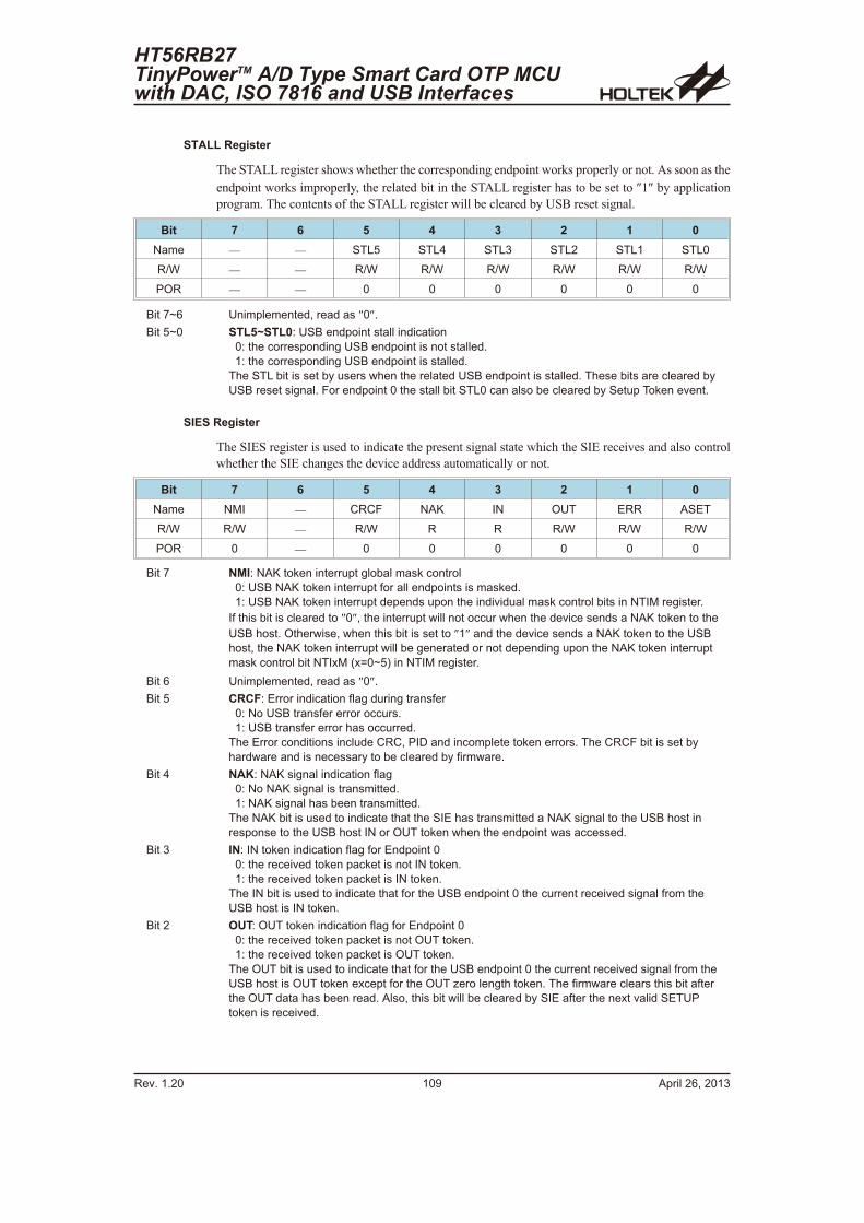
STALL Register
The STALL register shows whether the corresponding endpoint works properly or not. As soon as the
endpoint works improperly, the related bit in the STALL register has to be set to �1� by application
program. The contents of the STALL register will be cleared by USB reset signal.
Bit 7 6 5 4 3 2 1 0
Name � � STL5 STL4 STL3 STL2 STL1 STL0
R/W � � R/W R/W R/W R/W R/W R/W
POR � � 0 0 0 0 0 0
Bit 7~6 Unimplemented, read as �0�.
Bit 5~0 STL5~STL0: USB endpoint stall indication
0: the corresponding USB endpoint is not stalled.
1: the corresponding USB endpoint is stalled.
The STL bit is set by users when the related USB endpoint is stalled. These bits are cleared by
USB reset signal. For endpoint 0 the stall bit STL0 can also be cleared by Setup Token event.
SIES Register
The SIES register is used to indicate the present signal state which the SIE receives and also control
whether the SIE changes the device address automatically or not.
Bit 7 6 5 4 3 2 1 0
Name NMI � CRCF NAK IN OUT ERR ASET
R/W R/W � R/W R R R/W R/W R/W
POR 0 � 0 0 0 0 0 0
Bit 7 NMI: NAK token interrupt global mask control
0: USB NAK token interrupt for all endpoints is masked.
1: USB NAK token interrupt depends upon the individual mask control bits in NTIM register.
If this bit is cleared to �0�, the interrupt will not occur when the device sends a NAK token to the
USB host. Otherwise, when this bit is set to �1� and the device sends a NAK token to the USB
host, the NAK token interrupt will be generated or not depending upon the NAK token interrupt
mask control bit NTIxM (x=0~5) in NTIM register.
Bit 6 Unimplemented, read as �0�.
Bit 5 CRCF: Error indication flag during transfer
0: No USB transfer error occurs.
1: USB transfer error has occurred.
The Error conditions include CRC, PID and incomplete token errors. The CRCF bit is set by
hardware and is necessary to be cleared by firmware.
Bit 4 NAK: NAK signal indication flag
0: No NAK signal is transmitted.
1: NAK signal has been transmitted.
The NAK bit is used to indicate that the SIE has transmitted a NAK signal to the USB host in
response to the USB host IN or OUT token when the endpoint was accessed.
Bit 3 IN: IN token indication flag for Endpoint 0
0: the received token packet is not IN token.
1: the received token packet is IN token.
The IN bit is used to indicate that for the USB endpoint 0 the current received signal from the
USB host is IN token.
Bit 2 OUT: OUT token indication flag for Endpoint 0
0: the received token packet is not OUT token.
1: the received token packet is OUT token.
The OUT bit is used to indicate that for the USB endpoint 0 the current received signal from the
USB host is OUT token except for the OUT zero length token. The firmware clears this bit after
the OUT data has been read. Also, this bit will be cleared by SIE after the next valid SETUP
token is received.
HT56RB27TinyPowerTM A/D Type Smart Card OTP MCUwith DAC, ISO 7816 and USB Interfaces
Rev. 1.20 109 April 26, 2013
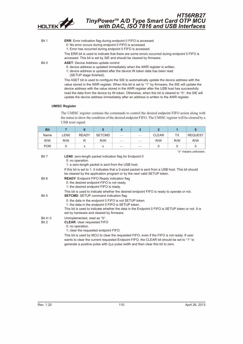
Bit 1 ERR: Error indication flag during endpoint 0 FIFO is accessed
0: No error occurs during endpoint 0 FIFO is accessed.
1: Error has occurred during endpoint 0 FIFO is accessed.
The ERR bit is used to indicate that there are some errors occurred during endpoint 0 FIFO is
accessed. This bit is set by SIE and should be cleared by firmware.
Bit 0 ASET: Device Address update control
0: device address is updated immediately when the AWR register is written.
1: device address is updated after the device IN token data has been read
(SETUP stage finished).
The ASET bit is used to configure the SIE to automatically update the device address with the
value stored in the AWR register. When this bit is set to �1� by firmware, the SIE will update the
device address with the value stored in the AWR register after the USB host has successfully
read the data from the device by IN token. Otherwise, when this bit is cleared to �0�, the SIE will
update the device address immediately after an address is written to the AWR register.
UMISC Register
The UMISC register contains the commands to control the desired endpoint FIFO action along with
the status to show the condition of the desired endpoint FIFO. The UMISC register will be cleared by a
USB reset signal.
Bit 7 6 5 4 3 2 1 0
Name LEN0 READY SETCMD � � CLEAR TX REQUEST
R/W R/W R R/W � � R/W R/W R/W
POR 0 x x � � 0 0 0
�x� means unknown.
Bit 7 LEN0: zero-length packet indication flag for Endpoint 0
0: no operation.
1: a zero-length packet is sent from the USB host.
If this bit is set to 1, it indicates that a 0-sized packet is sent from a USB host. This bit should
be cleared by the application program or by the next valid SETUP token.
Bit 6 READY: Endpoint FIFO Ready indication flag
0: the desired endpoint FIFO is not ready.
1: the desired endpoint FIFO is ready.
This bit is used to indicate whether the desired endpoint FIFO is ready to operate or not.
Bit 5 SETCMD: SETUP command indication flag
0: the data in the endpoint 0 FIFO is not SETUP token.
1: the data in the endpoint 0 FIFO is SETUP token.
This bit is used to indicate whether the data in the Endpoint 0 FIFO is SETUP token or not. It is
set by hardware and cleared by firmware.
Bit 4~3 Unimplemented, read as �0�.
Bit 2 CLEAR: clear requested FIFO
0: no operation.
1: clear the requested endpoint FIFO.
This bit is used by MCU to clear the requested FIFO, even if the FIFO is not ready. If user
wants to clear the current requested Endpoint FIFO, the CLEAR bit should be set to �1� to
generate a positive pulse with 2�s pulse width and then clear this bit to zero.
Rev. 1.20 110 April 26, 2013
HT56RB27TinyPowerTM A/D Type Smart Card OTP MCU
with DAC, ISO 7816 and USB Interfaces
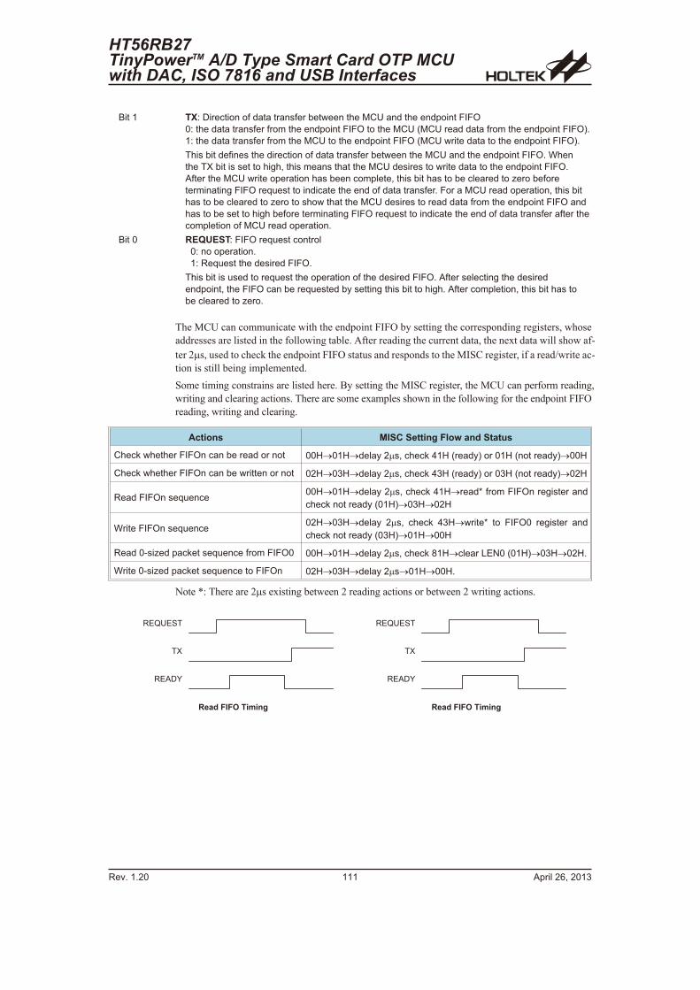
Bit 1 TX: Direction of data transfer between the MCU and the endpoint FIFO
0: the data transfer from the endpoint FIFO to the MCU (MCU read data from the endpoint FIFO).
1: the data transfer from the MCU to the endpoint FIFO (MCU write data to the endpoint FIFO).
This bit defines the direction of data transfer between the MCU and the endpoint FIFO. When
the TX bit is set to high, this means that the MCU desires to write data to the endpoint FIFO.
After the MCU write operation has been complete, this bit has to be cleared to zero before
terminating FIFO request to indicate the end of data transfer. For a MCU read operation, this bit
has to be cleared to zero to show that the MCU desires to read data from the endpoint FIFO and
has to be set to high before terminating FIFO request to indicate the end of data transfer after the
completion of MCU read operation.
Bit 0 REQUEST: FIFO request control
0: no operation.
1: Request the desired FIFO.
This bit is used to request the operation of the desired FIFO. After selecting the desired
endpoint, the FIFO can be requested by setting this bit to high. After completion, this bit has to
be cleared to zero.
The MCU can communicate with the endpoint FIFO by setting the corresponding registers, whose
addresses are listed in the following table. After reading the current data, the next data will show af-
ter 2�s, used to check the endpoint FIFO status and responds to the MISC register, if a read/write ac-
tion is still being implemented.
Some timing constrains are listed here. By setting the MISC register, the MCU can perform reading,
writing and clearing actions. There are some examples shown in the following for the endpoint FIFO
reading, writing and clearing.
Actions MISC Setting Flow and Status
Check whether FIFOn can be read or not 00H�01H�delay 2�s, check 41H (ready) or 01H (not ready)�00H
Check whether FIFOn can be written or not 02H�03H�delay 2�s, check 43H (ready) or 03H (not ready)�02H
Read FIFOn sequence00H�01H�delay 2�s, check 41H�read* from FIFOn register and
check not ready (01H)�03H�02H
Write FIFOn sequence02H�03H�delay 2�s, check 43H�write* to FIFO0 register and
check not ready (03H)�01H�00H
Read 0-sized packet sequence from FIFO0 00H�01H�delay 2�s, check 81H�clear LEN0 (01H)�03H�02H.
Write 0-sized packet sequence to FIFOn 02H�03H�delay 2�s�01H�00H.
Note *: There are 2�s existing between 2 reading actions or between 2 writing actions.
HT56RB27TinyPowerTM A/D Type Smart Card OTP MCUwith DAC, ISO 7816 and USB Interfaces
Rev. 1.20 111 April 26, 2013
� F > � # �
� D
� , � -
, � � � / � / - � # � � � � �
� F > � # �
� D
� , � -
, � � � / � / - � # � � � � �
SETIO Register
The SETIO register is used to configure the endpoint FIFO as IN pipe or OUT pipe.
Bit 7 6 5 4 3 2 1 0
Name � � SETIO5 SETIO4 SETIO3 SETIO2 SETIO1 DATATG
R/W � � R/W R/W R/W R/W R/W R/W
POR � � 1 1 1 1 1 0
Bit 7~6 Unimplemented, read as �0�.
Bit 5~1 SETIO5~SETIO1: Endpoint 5 FIFO ~ Endpoint FIFO1 pipe direction control.
0: the corresponding endpoint FIFO is configured as OUT pipe.
1: the corresponding endpoint FIFO is configured as IN pipe.
If the related SETIO bit is set to �1�, the corresponding endpoint FIFO is configured as IN pipe
for IN token operation. Otherwise, the corresponding endpoint FIFO is configured as OUT pipe
for OUT token operation. The purpose of this function is to avoid the USB host from abnormally
sending only an IN token or OUT token and disable the related endpoint.
Bit 0 DATATG: DATA0 toggle bit
0: no operation.
1: DATA0 will be sent first.
As the USB specification defined, when the USB host sends a �Set Configuration� SETUP
token, the Data pipe should send the DATA0 (Data toggle) first. Therefore, when the USB device
receives a �Set Configuration� SETUP token, user needs to set DATATG bit to �1� and then
clear it to zero after a 2�s delay to generate a positive pulse with 2�s pulse width to make sure
that the next data will send a DATA0 first.
FIFO0~FIFO5 Registers
The FIFO0~FIFO5 Registers are used for data transactions between the USB device and the USB host.
The MCU reads data from or writes data to the FIFOs via the application program to complete data
interchange. For �Interrupt transfer� it is supported by FIFO0~FIFO2 and FIFO4, while it is supported
by FIFO3 and FIFO5 for �Bulk transfer�.
Label Type POR UMISC Setting Flow and Status
FIFO0 R/W xxxx xxxx Data pipe for endpoint 0, depth = 8 bytes
FIFO1 R/W xxxx xxxx Data pipe for endpoint 1, depth = 8 bytes
FIFO2 R/W xxxx xxxx Data pipe for endpoint 2, depth = 8 bytes
FIFO3 R/W xxxx xxxx Data pipe for endpoint 3, depth = 64 bytes
FIFO4 R/W xxxx xxxx Data pipe for endpoint 4, depth = 8 bytes
FIFO5 R/W xxxx xxxx Data pipe for endpoint 5, depth = 64 bytes
�x� means unknown.
Rev. 1.20 112 April 26, 2013
HT56RB27TinyPowerTM A/D Type Smart Card OTP MCU
with DAC, ISO 7816 and USB Interfaces
UIC Register
The UIC register is used to control the interrupt request for each endpoint. Interrupts can be enabled or
disabled independently if the corresponding endpoint FIFO pipes are enabled.
Bit 7 6 5 4 3 2 1 0
Name � � EU5I EU4I EU3I EU2I EU1I EU0I
R/W � � R/W R/W R/W R/W R/W R/W
POR � � 0 0 0 0 0 0
Bit 7~6 Unimplemented, read as �0�.
Bit 5~0 EU5I~EU0I: USB Endpoint 5 ~ Endpoint 0 interrupt control as being accessed.
0: disable the corresponding endpoint interrupt as it is accessed.
1: enable the corresponding endpoint interrupt as it is accessed.
If the related Endpoint FIFO pipe is enabled and the corresponding Endpoint interrupt is
enabled, the USB interrupt for endpoint access will occur. Then an interrupt signal pulse will be
generated sent to MCU to get the attentions from the host MCU.
NTIM Register
The NTIM register is used to control the NAK token interrupt for each endpoint. The NAK token
interrupt can be masked independently by controlling the NTIM register if the NAK token interrupt
global mask control NMI in SIES register is set to 1.
Bit 7 6 5 4 3 2 1 0
Name � � NTI5M NTI4M NTI3M NTI2M NTI1M NTI0M
R/W � � R/W R/W R/W R/W R/W R/W
POR � � 0 0 0 0 0 0
Bit 7~6 Unimplemented, read as �0�.
Bit 5~0 NTI5M~NTI0M: USB Endpoint 5 ~ Endpoint 0 NAK Token Interrupt Mask control.
0: the corresponding endpoint NAK token interrupt is not masked.
1: the corresponding endpoint NAK token interrupt is masked.
If the NAK Token Interrupt global mask control is set to �1� and the corresponding Endpoint NAK
token interrupt is not masked, the NAK token interrupt will occur when the USB device sends a
NAK token to the USB host. Then an interrupt signal pulse will be generated sent to the host
MCU to get the attentions from the host MCU.
HT56RB27TinyPowerTM A/D Type Smart Card OTP MCUwith DAC, ISO 7816 and USB Interfaces
Rev. 1.20 113 April 26, 2013
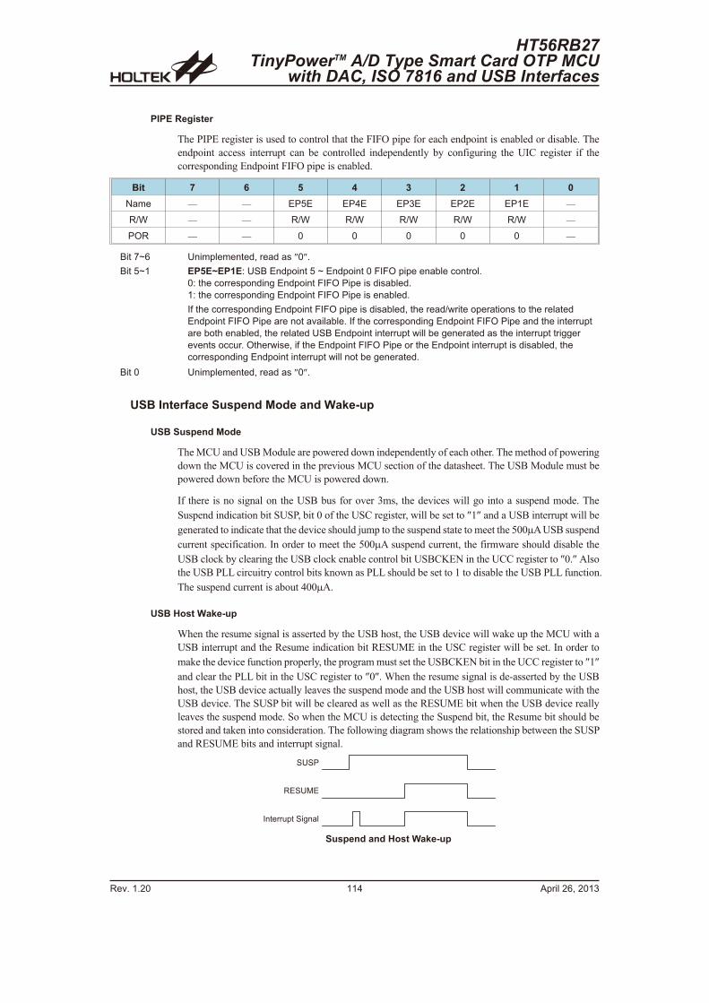
PIPE Register
The PIPE register is used to control that the FIFO pipe for each endpoint is enabled or disable. The
endpoint access interrupt can be controlled independently by configuring the UIC register if the
corresponding Endpoint FIFO pipe is enabled.
Bit 7 6 5 4 3 2 1 0
Name � � EP5E EP4E EP3E EP2E EP1E �
R/W � � R/W R/W R/W R/W R/W �
POR � � 0 0 0 0 0 �
Bit 7~6 Unimplemented, read as �0�.
Bit 5~1 EP5E~EP1E: USB Endpoint 5 ~ Endpoint 0 FIFO pipe enable control.
0: the corresponding Endpoint FIFO Pipe is disabled.
1: the corresponding Endpoint FIFO Pipe is enabled.
If the corresponding Endpoint FIFO pipe is disabled, the read/write operations to the related
Endpoint FIFO Pipe are not available. If the corresponding Endpoint FIFO Pipe and the interrupt
are both enabled, the related USB Endpoint interrupt will be generated as the interrupt trigger
events occur. Otherwise, if the Endpoint FIFO Pipe or the Endpoint interrupt is disabled, the
corresponding Endpoint interrupt will not be generated.
Bit 0 Unimplemented, read as �0�.
USB Interface Suspend Mode and Wake-up
USB Suspend Mode
The MCU and USB Module are powered down independently of each other. The method of powering
down the MCU is covered in the previous MCU section of the datasheet. The USB Module must be
powered down before the MCU is powered down.
If there is no signal on the USB bus for over 3ms, the devices will go into a suspend mode. The
Suspend indication bit SUSP, bit 0 of the USC register, will be set to �1� and a USB interrupt will be
generated to indicate that the device should jump to the suspend state to meet the 500�A USB suspend
current specification. In order to meet the 500�A suspend current, the firmware should disable the
USB clock by clearing the USB clock enable control bit USBCKEN in the UCC register to �0.� Also
the USB PLL circuitry control bits known as PLL should be set to 1 to disable the USB PLL function.
The suspend current is about 400�A.
USB Host Wake-up
When the resume signal is asserted by the USB host, the USB device will wake up the MCU with a
USB interrupt and the Resume indication bit RESUME in the USC register will be set. In order to
make the device function properly, the program must set the USBCKEN bit in the UCC register to �1�
and clear the PLL bit in the USC register to �0�. When the resume signal is de-asserted by the USB
host, the USB device actually leaves the suspend mode and the USB host will communicate with the
USB device. The SUSP bit will be cleared as well as the RESUME bit when the USB device really
leaves the suspend mode. So when the MCU is detecting the Suspend bit, the Resume bit should be
stored and taken into consideration. The following diagram shows the relationship between the SUSP
and RESUME bits and interrupt signal.
Rev. 1.20 114 April 26, 2013
HT56RB27TinyPowerTM A/D Type Smart Card OTP MCU
with DAC, ISO 7816 and USB Interfaces
# > # �
� # > / �
� � � � ! ! � ( � � # � % � � �
Suspend and Host Wake-up
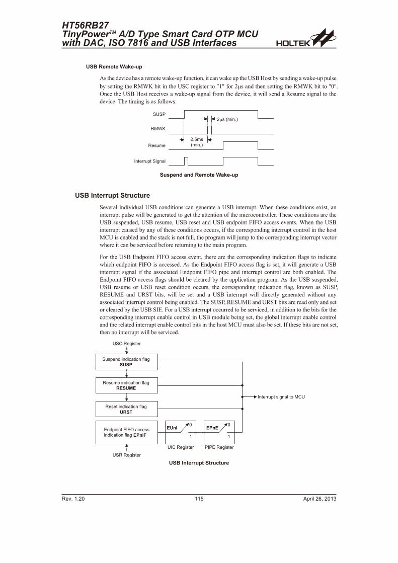
USB Remote Wake-up
As the device has a remote wake-up function, it can wake up the USB Host by sending a wake-up pulse
by setting the RMWK bit in the USC register to �1� for 2�s and then setting the RMWK bit to �0�.
Once the USB Host receives a wake-up signal from the device, it will send a Resume signal to the
device. The timing is as follows:
USB Interrupt Structure
Several individual USB conditions can generate a USB interrupt. When these conditions exist, an
interrupt pulse will be generated to get the attention of the microcontroller. These conditions are the
USB suspended, USB resume, USB reset and USB endpoint FIFO access events. When the USB
interrupt caused by any of these conditions occurs, if the corresponding interrupt control in the host
MCU is enabled and the stack is not full, the program will jump to the corresponding interrupt vector
where it can be serviced before returning to the main program.
For the USB Endpoint FIFO access event, there are the corresponding indication flags to indicate
which endpoint FIFO is accessed. As the Endpoint FIFO access flag is set, it will generate a USB
interrupt signal if the associated Endpoint FIFO pipe and interrupt control are both enabled. The
Endpoint FIFO access flags should be cleared by the application program. As the USB suspended,
USB resume or USB reset condition occurs, the corresponding indication flag, known as SUSP,
RESUME and URST bits, will be set and a USB interrupt will directly generated without any
associated interrupt control being enabled. The SUSP, RESUME and URST bits are read only and set
or cleared by the USB SIE. For a USB interrupt occurred to be serviced, in addition to the bits for the
corresponding interrupt enable control in USB module being set, the global interrupt enable control
and the related interrupt enable control bits in the host MCU must also be set. If these bits are not set,
then no interrupt will be serviced.
HT56RB27TinyPowerTM A/D Type Smart Card OTP MCUwith DAC, ISO 7816 and USB Interfaces
Rev. 1.20 115 April 26, 2013
# > # �
� � � � �
/ C B
� � � � ! ! � ( � � # � % � � �
� � � � � � � � � �
� � ) � �� � � � � �
Suspend and Remote Wake-up
> # � � � % � � � � !
> # � � % � � � � !
7
�
) � � �7
�
) � � )
� � � � ! ! � ( � � � � % � � � � � � / � >
> � � � � % � � � � ! � � � � � � % � � � � !
� � ; ( � � � � � � � � � � � �� � ; � � � � � � : � � % � ) � � � / �
� � � � � � � ; � � � � � � : � � % �
� , � #
� � � � � � � � ; � � � � � � : � � % �
, ) � � � )
# � � ( � � ; � � � ; � � � � � � : � � % �
� � � �
USB Interrupt Structure
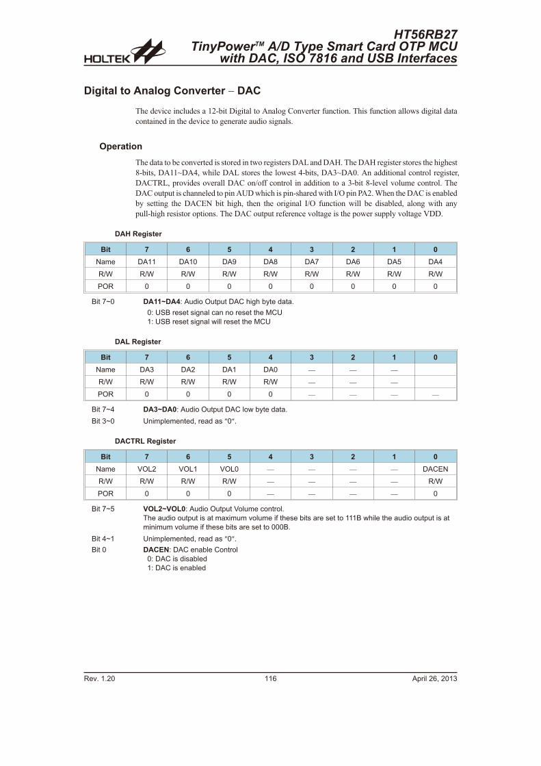
Digital to Analog Converter � DAC
The device includes a 12-bit Digital to Analog Converter function. This function allows digital data
contained in the device to generate audio signals.
Operation
The data to be converted is stored in two registers DAL and DAH. The DAH register stores the highest
8-bits, DA11~DA4, while DAL stores the lowest 4-bits, DA3~DA0. An additional control register,
DACTRL, provides overall DAC on/off control in addition to a 3-bit 8-level volume control. The
DAC output is channeled to pin AUD which is pin-shared with I/O pin PA2. When the DAC is enabled
by setting the DACEN bit high, then the original I/O function will be disabled, along with any
pull-high resistor options. The DAC output reference voltage is the power supply voltage VDD.
DAH Register
Bit 7 6 5 4 3 2 1 0
Name DA11 DA10 DA9 DA8 DA7 DA6 DA5 DA4
R/W R/W R/W R/W R/W R/W R/W R/W R/W
POR 0 0 0 0 0 0 0 0
Bit 7~0 DA11~DA4: Audio Output DAC high byte data.
0: USB reset signal can no reset the MCU
1: USB reset signal will reset the MCU
DAL Register
Bit 7 6 5 4 3 2 1 0
Name DA3 DA2 DA1 DA0 � � �
R/W R/W R/W R/W R/W � � �
POR 0 0 0 0 � � � �
Bit 7~4 DA3~DA0: Audio Output DAC low byte data.
Bit 3~0 Unimplemented, read as �0�.
DACTRL Register
Bit 7 6 5 4 3 2 1 0
Name VOL2 VOL1 VOL0 � � � � DACEN
R/W R/W R/W R/W � � � � R/W
POR 0 0 0 � � � � 0
Bit 7~5 VOL2~VOL0: Audio Output Volume control.
The audio output is at maximum volume if these bits are set to 111B while the audio output is at
minimum volume if these bits are set to 000B.
Bit 4~1 Unimplemented, read as �0�.
Bit 0 DACEN: DAC enable Control
0: DAC is disabled
1: DAC is enabled
Rev. 1.20 116 April 26, 2013
HT56RB27TinyPowerTM A/D Type Smart Card OTP MCU
with DAC, ISO 7816 and USB Interfaces
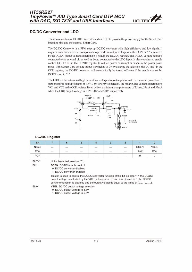
DC/DC Converter and LDO
The device contains a DC/DC Converter and an LDO to provide the power supply for the Smart Card
interface pins and the external Smart Card.
The DC/DC Converter is a PFM step-up DC/DC converter with high efficiency and low ripple. It
requires only three external components to provide an output voltage of either 3.8V or 5.5V selected
by the DC/DC output voltage selection bit VSEL in the DC2DC register. The DC/DC voltage output is
connected to an external pin as well as being connected to the LDO input. It also contains an enable
control bit, DCEN, in the DC2DC register to reduce power consumption when in the power down
mode. If the Smart Card voltage output is switched to 0V by clearing the selection bits VC [1:0] in the
CCR register, the DC/DC converter will automatically be turned off even if the enable control bit
DCEN is set to �1�.
The LDO is a three-terminal high current low voltage dropout regulator with over current protection. It
supports three output voltages of 1.8V, 3.0V or 5.0V selected by the Smart Card Voltage selection bits
VC1 and VC0 in the CCR register. It can deliver a minimum output current of 35mA, 55mAand 55mA
when the LDO output voltage is 1.8V, 3.0V and 5.0V respectively.
DC2DC Register
Bit 7 6 5 4 3 2 1 0
Name � � � � � � DCEN VSEL
R/W � � � � � � R/W R/W
POR � � � � � � 0 0
Bit 7~2 Unimplemented, read as �0�.
Bit 1 DCEN: DC/DC enable control
0: DC/DC converter disabled
1: DC/DC converter enabled
This bit is used to control the DC/DC converter function. If this bit is set to �1�, the DC/DC
output voltage is selected by the VSEL selection bit. If this bit is cleared to 0, the DC/DC
converter function is disabled and the output voltage is equal to the value of (VDD� VDIODE).
Bit 0 VSEL: DC/DC output voltage selection
0: DC/DC output voltage is 3.8V
1: DC/DC output voltage is 5.5V
HT56RB27TinyPowerTM A/D Type Smart Card OTP MCUwith DAC, ISO 7816 and USB Interfaces
Rev. 1.20 117 April 26, 2013
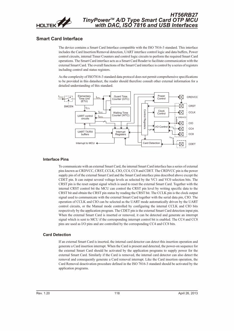
Smart Card Interface
The device contains a Smart Card Interface compatible with the ISO 7816-3 standard. This interface
includes the Card Insertion/Removal detection, UART interface control logic and data buffers, Power
control circuits, internal Timer Counters and control logic circuits to perform the required Smart Card
operations. The Smart Card interface acts as a Smart Card Reader to facilitate communication with the
external Smart Card. The overall functions of the Smart Card interface is control by a series of registers
including control and status registers.
As the complexity of ISO7816-3 standard data protocol does not permit comprehensive specifications
to be provided in this datasheet, the reader should therefore consult other external information for a
detailed understanding of this standard.
Interface Pins
To communicate with an external Smart Card, the internal Smart Card interface has a series of external
pins known as CRDVCC, CRST, CCLK, CIO, CC4, CC8 and CDET. The CRDVCC pin is the power
supply pin of of the external Smart Card and the Smart Card interface pins described above except the
CDET pin. It can output several voltage levels as selected by the VC1 and VC0 selection bits. The
CRST pin is the reset output signal which is used to reset the external Smart Card. Together with the
internal CRST control bit the MCU can control the CRST pin level by writing specific data to the
CRST bit and obtain the CRST pin status by reading the CRST bit. The CCLK pin is the clock output
signal used to communicate with the external Smart Card together with the serial data pin, CIO. The
operation of CCLK and CIO can be selected as the UART mode automatically driven by the UART
control circuits, or the Manual mode controlled by configuring the internal CCLK and CIO bits
respectively by the application program. The CDET pin is the external Smart Card detection input pin.
When the external Smart Card is inserted or removed, it can be detected and generate an interrupt
signal which is sent to MCU if the corresponding interrupt control bit is enabled. The CC4 and CC8
pins are used as I/O pins and are controlled by the corresponding CC4 and CC8 bits.
Card Detection
If an external Smart Card is inserted, the internal card detector can detect this insertion operation and
generate a Card insertion interrupt. When the Card is present and detected, the power-on sequence for
the external Smart Card should be activated by the application programs to supply power for the
external Smart Card. Similarly if the Card is removed, the internal card detector can also detect the
removal and consequently generate a Card removal interrupt. Like the Card insertion operation, the
Card Removal deactivation procedure defined in the ISO 7816-3 standard should be activated by the
application programs.
Rev. 1.20 118 April 26, 2013
HT56RB27TinyPowerTM A/D Type Smart Card OTP MCU
with DAC, ISO 7816 and USB Interfaces
CRDVCCElementaryTime Unit
(ETU)
Guard TimeCounter (GTC)
Waiting TimeCounter (WTC)
fCCLK
UART controlcircuits
UART TX/RXbuffers
InterruptRegisters
Interrupt to MCU
PowerControl
CDETCard Detection
CRST
CCLK
CIO
CC4
CC8
I/O Control
ClockControl
fETU
fETU
fGTC
fWTC
Co
ntro
lR
egis
ters
CRDVCC
VDD
SMCEN
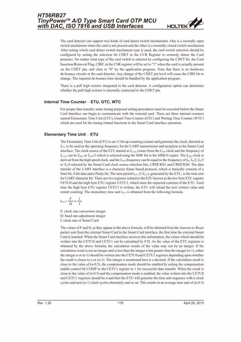
The card detector can support two kinds of card detect switch mechanisms. One is a normally open
switch mechanism when the card is not present and the other is a normally closed switch mechanism.
After noting which card detect switch mechanism type is used, the card switch selection should be
configured by setting the selection bit CDET in the CCR Register to correctly detect the Card
presence. No matter what type of the card switch is selected by configuring the CDET bit, the Card
Insertion/Removal Flag, CIRF, in the CSR register will be set to �1� when the card is actually present
on the CDET pin, and clear to �0� by the application program. Note that there is no hardware
de-bounce circuits in the card detector. Any change of the CDET pin level will cause the CIRF bit to
change. The required de-bounce time should be handled by the application program.
There is a pull high resistor integrated in the card detector. A configuration option can determine
whether the pull high resistor is internally connected to the CDET pin.
Internal Time Counter � ETU, GTC, WTC
For proper data transfer, some timing purposed setting procedures must be executed before the Smart
Card Interface can begin to communicate with the external card. There are three internal counters
named Elementary Time Unit (ETU), Guard Time Counter (GTC) and Waiting Time Counter (WTC)
which are used for the timing related functions in the Smart Card interface operation.
Elementary Time Unit � ETU
The Elementary Time Unit (ETU) is an 11-bit up-counting counter and generates the clock, denoted as
fETU to be used as the operating frequency for the UART transmission and reception in the Smart Card
interface. The clock source of the ETU named as fCCLK comes from the fCRD clock and the frequency of
fCCLK can be fCRD or fCRD/2 which is selected using the SMF bit in the MISC0 regiter. The fCRD clock is
derived from the high speed clock, and the fCRD frequency can be equal to the frequency of fM, fM/2, fM/3
or fM/4 selected by the Smart Card clock source selection bits, CRDCKS1 and CRDCKS0. The data
transfer of the UART interface is a character frame based protocol, which is basically consists of a
Start bit, 8-bit data and a Parity bit. The time period tETU (1/fETU), generated by the ETU, is the time unit
for UART character bit. There are two registers related to the ETU known as the low byte ETU register
CETU0 and the high byte ETU register CETU1, which store the expected contents of the ETU. Each
time the high byte ETU register CETU1 is written, the ETU will reload the new written value and
restart counting. The elementary time unit tETU is obtained from the following formula.
tETU=F
Dx
1
f
F: clock rate conversion integer
D: baud rate adjustment integer
f: clock rate of Smart Card
The values of F and D, as they appear in the above formula, will be obtained from the Answer-to-Reset
packet sent from the external Smart Card to the Smart Card interface, the first time the external Smart
Card is inserted. When the Smart Card interface receives this information, the values which should be
written into the CETU0 and CETU1 can be calculated by F/D. As the value of the ETU registers is
obtained by the above formula, the calculation results of the value may not be an integer. If the
calculation result is not an integer and is less than the integer n but greater than the integer (n-1), either
the integer n or (n-1) should be written into the CETU0 and CETU1 registers depending upon whether
the result is closer to n or (n-1). The integer n mentioned here is a decimal. If the calculation result is
close to the value of (n-0.5), the compensation mode should be enabled by setting the compensation
enable control bit COMP in the CETU1 register to 1 for successful data transfer. When the result is
close to the value of (n-0.5) and the compensation mode is enabled, the value written into the CETU0
and CETU1 registers should be n and then the ETU will generate the time unit sequence with n clock
cycles and next (n-1) clock cycles alternately and so on. This results in an average time unit of (n-0.5)
HT56RB27TinyPowerTM A/D Type Smart Card OTP MCUwith DAC, ISO 7816 and USB Interfaces
Rev. 1.20 119 April 26, 2013
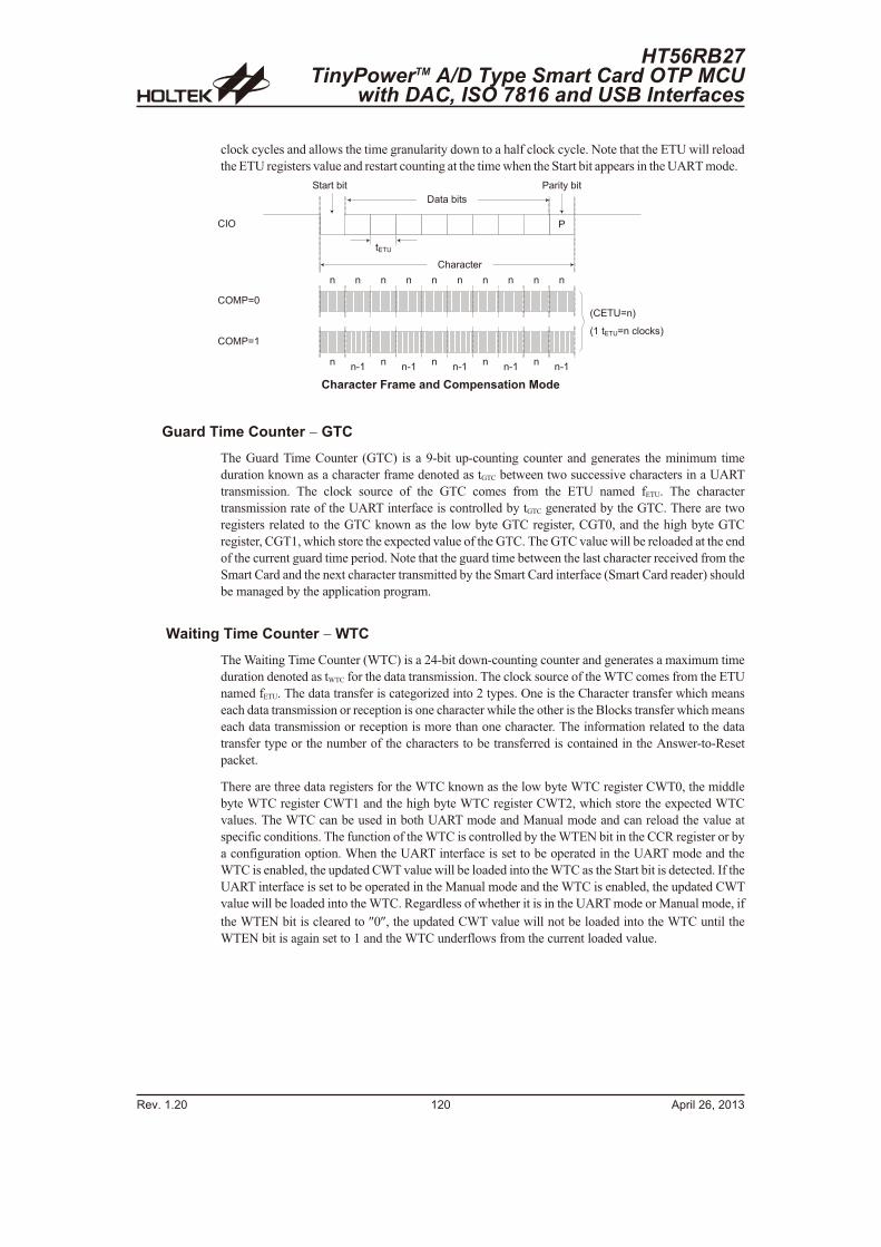
clock cycles and allows the time granularity down to a half clock cycle. Note that the ETU will reload
the ETU registers value and restart counting at the time when the Start bit appears in the UART mode.
Guard Time Counter � GTC
The Guard Time Counter (GTC) is a 9-bit up-counting counter and generates the minimum time
duration known as a character frame denoted as tGTC between two successive characters in a UART
transmission. The clock source of the GTC comes from the ETU named fETU. The character
transmission rate of the UART interface is controlled by tGTC generated by the GTC. There are two
registers related to the GTC known as the low byte GTC register, CGT0, and the high byte GTC
register, CGT1, which store the expected value of the GTC. The GTC value will be reloaded at the end
of the current guard time period. Note that the guard time between the last character received from the
Smart Card and the next character transmitted by the Smart Card interface (Smart Card reader) should
be managed by the application program.
Waiting Time Counter � WTC
The Waiting Time Counter (WTC) is a 24-bit down-counting counter and generates a maximum time
duration denoted as tWTC for the data transmission. The clock source of the WTC comes from the ETU
named fETU. The data transfer is categorized into 2 types. One is the Character transfer which means
each data transmission or reception is one character while the other is the Blocks transfer which means
each data transmission or reception is more than one character. The information related to the data
transfer type or the number of the characters to be transferred is contained in the Answer-to-Reset
packet.
There are three data registers for the WTC known as the low byte WTC register CWT0, the middle
byte WTC register CWT1 and the high byte WTC register CWT2, which store the expected WTC
values. The WTC can be used in both UART mode and Manual mode and can reload the value at
specific conditions. The function of the WTC is controlled by the WTEN bit in the CCR register or by
a configuration option. When the UART interface is set to be operated in the UART mode and the
WTC is enabled, the updated CWT value will be loaded into the WTC as the Start bit is detected. If the
UART interface is set to be operated in the Manual mode and the WTC is enabled, the updated CWT
value will be loaded into the WTC. Regardless of whether it is in the UART mode or Manual mode, if
the WTEN bit is cleared to �0�, the updated CWT value will not be loaded into the WTC until the
WTEN bit is again set to 1 and the WTC underflows from the current loaded value.
Rev. 1.20 120 April 26, 2013
HT56RB27TinyPowerTM A/D Type Smart Card OTP MCU
with DAC, ISO 7816 and USB Interfaces
CIO
Start bit
P
Parity bit
Character
COMP=0
COMP=1
n n n n n n n n n n
nn-1
n n n nn-1 n-1 n-1 n-1
(1 tETU=n clocks)
(CETU=n)
tETU
Data bits
Character Frame and Compensation Mode
When the transfer type is configured as a Character transfer, the WTC will generate the maximum
timeout period of the Character Waiting Time (CWT). If the transfer type is configured as a Block
transfer, the WTC will generate the Character Waiting Time (CWT) except for the last character. The
Block Waiting Time (BWT) should be loaded into the WTC data registers before the Start bit of the
last transmitted character occurs. As the Start bit of the last transmitted character occurs, the BWT
value will be load into the WTC. Then the Smart Card may be expected to transmit data to the Smart
Card interface in the BWT duration. If the Smart Card does not transmit any data characters, the WTC
will underflow. When the WTC underflows, the corresponding request flag, WTF, in the CSR register
will be set. The Waiting Time Underflow pending flag, WTP, in the CIPR register, will also be set if the
interrupt enable control bit, WTE, in the CIER register is set. Then an interrupt will be generated to
notify the MCU that the Smart Card has not responded to the Smart Card reader. Note that if the WTC
value is set to zero, the WFT bit will be equal to �1�.
UART Interface
Data transfer with the external Smart Card is implemented into two operating modes. One is the UART
mode while the other is the Manual mode. The data transfer mode is selected by the UART mode
selection bit, UMOD, in the CCR register. When the UMOD bit is set to �1�, the UART mode is
enabled and data transfer operates in the UART mode. Otherwise, data transfer operates in the Manual
mode if the UMOD bit is set to �0�. The UART interface is a half-duplex interface and communicates
with the external Smart Card via the CCLK and CIO pins. The CIO pin can be selected to be connected
to a pull high resistor by a configuration option. After a reset condition the UART interface is in the
reception mode but the UART mode is disabled. When the UART mode is selected, data transfer is
driven by the UART circuits automatically through the CCLK and CIO pins.
There are two data registers related to data transmission and reception, CTXB and CRXB, which store
the data to be transmitted and received respectively. If a character is written into the CTXB register in
the UART mode, the UART interface will automatically switch to the transmission mode from the
reception mode after a reset. When the UART transmission or reception has finished, the
corresponding request flag named TXCF or RXCF is set to �1�. If the transmit buffer is empty, the
transmit buffer empty flag, TXBEF, will be set to �1�.
The UART interface supports a parity generator and a parity check function. As the parity error occurs
during a data transfer, the corresponding request flag named, PARF, in the CSR register will be set to
�1�. Once the PARF bit is set to �1�, the Parity error pending flag PARP in the CIPR register will be set
to �1� if the relevant interrupt control bit is enabled. Then an interrupt signal will be generated and sent
to the MCU.
There is a Character Repetition function supported by the UART interface when a parity error occurs.
The Character repetition function is enabled by setting the CREP bit to �1� and then the repetition
function is activated when the parity error occurs during data transfers. The repetition times can be
selected to be 4 or 5 times by a configuration option. When the CREP bit is set to �1� and the repetition
times is set to 4 times, the UART interface, if in the transmission mode, will transmit the data
repeatedly for 4 times at most when an error signal occurs. If the data transmitted by the UART
interface is received by the Smart Card receiver without a parity error during these 4 transmissions, the
HT56RB27TinyPowerTM A/D Type Smart Card OTP MCUwith DAC, ISO 7816 and USB Interfaces
Rev. 1.20 121 April 26, 2013
Smart CardInterface
Smart Card
Char 0 Char 1 Char n
Programthe BWT
BWT
Programthe CWT
Char 1
CWT
Start bit
Start bit
Char 0
WTC is reloaded on Start bit
transmission request flag, TXCF, of the UART interface will be set to �1� and the PARF bit will be
cleared to �0�. If the UART interface is informed that there is still an error signal during the 4
transmissions, the parity error flag PARF of the UART interface will be set to �1� at the 5th
transmission but the transmission request flag TXCF will not be set. If the UART interface is in the
reception mode, it will inform the Smart Card transmitter that there is a parity error for at most 4 times.
If the data transmitted by the Smart Card transmitter is received by the UART interface without a
parity error during the 4 receptions, the reception request flag, RXCF, of the UART interface will be
set to �1� and the PARF bit will be cleared to �0�. If the UART interface informs the Smart Card that
there is still an error signal during the 4 receptions, the parity error flag, PARF, of the UART interface
will be set to �1� at the 5th reception as well as the transmission request flag, RXCF.
If the CREPbit is set to �0� and the UART interface is in the reception mode, both the PARF and RXCF
bits will be set to �1� when the data with parity error has been received but the character repetition will
not be activated. If the UART interface is in the transmission mode and the CREPbit is set to �0�, it acts
as a normal transmitter and the TXCF bit is set to �1� after the data has been transmitted. It has no effect
on PARF bit.
When data is selected to be transferred in the Manual mode by setting the UMOD bit to �0�, the data is
controlled by the control bit, CIO, in the CCCR register. The value of the CIO bit will be reflected
immediately on the CIO pin in the Manual mode. Note that in the Manual mode the character
repetition functions is not available as wll is the related flags and all t=he data transfer is handled by the
application program . The clock used to drive the external Smart Card that appears on the CCLK pin
can be the fCCLK clock which is derived from the internal clock source named as the fCRD clock or the
control bit, CCLK, in CCCR register and selected by the Smart Card selection bit, CLKSEL, in the
CCCR register. When CLKSEL is set to �1� to select the clock source for the Smart Card to be fCCLK, a
software control bit, SMF, can determine whether the clock output on the CCLK pin, which comes
from the fCRD clock, is moreover to be divided by 2 or not. If users wish to handle the CCLK clock
manually, the CLKSEL bit should first be set to 0 and then the value of the CCLK bit will be present on
the CCLK pin.
When the Smart Card is first inserted, the data direction convention is sent first in the Answer-to-Reset
packet to inform the Smart Card interface whether the MSB of the data is sent first or the LSB is sent
first. If the direction convention used by the Smart Card is the same as the convention used by the
Smart Card interface, the UART interface will generate a reception interrupt if the reception interrupt
is enabled without a parity error flag. Otherwise, the UART interface will generate a reception
interrupt and the parity error flag will be asserted. By checking the parity error flag the Smart Card
interface can know if the data direction convention is correct or not.
Power Control
When the Smart Card is first inserted and detected, the power-on sequence for the external Smart Card
should be activated by the application programs to supply power to the external Smart Card. All the
information necessary for the Smart Card interface to communicate with the external Card is contained
in the Answer-to-Reset packet including the data transfer type (Character or Blocks), the data direction
convention (MSB or LSB first), the clock rate information (ETU, GTC or WTC), etc. The voltage
level supplied to the Smart Card is also defined in the Answer-to-Reset packet. The Smart Card power
supply voltage level is generated by the LDO and selected by the Smart Card Power Supply voltage
selection bits VC1 and VC0 in the CCR register. When the external Smart Card is inserted, the
application program should set the CRDVCC pin to the expected voltage level defined in the
Answer-to-Reset packet. Similarly, the power deactivation procedure defined in the ISO 7816-3
standard should also be properly arranged by the application programs when the external Smart Card
is removed. After the external Smart Card is removed, the Smart Card Interface Circuitry enable
control bit, CVCC, in the CCCR Register will be automatically cleared to zero to prevent the Smart
Card Interface module from being re-modified. The CRDVCC pin voltage level and the related Smart
Card interface register contents will remain unchanged but the relevant Smart Card Interface pins
Rev. 1.20 122 April 26, 2013
HT56RB27TinyPowerTM A/D Type Smart Card OTP MCU
with DAC, ISO 7816 and USB Interfaces
including CRST, CCLK, CIO, CC4 and CC8 pins will be kept at a low level when the external Card is
removed.
The Power Control circuitry provides the Card voltage and current indicators to avoid malfunctions.
When the Card voltage is within its specified range, the Card Voltage flag VCOK will be set to �1�. If
the Card is not in the specified range, the VCOK flag will be cleared to �0� to indicate that the Card
voltage is not within the specified range. As the VCOK bit changes from 1 to 0, the corresponding
pending flag named VCP in CIPR register will be set to �1� if the Card Voltage error interrupt control
VCE in the CIER register is enabled.
When the current consumed by the external Smart Card is within the range specified in the ISO 7816-3
standard, the Card Current Overload flag IOVF will remain at a �0� value. If the Card current is not
within the specified range, the IOVF flag will be set to �1� to indicate that the Card Current is too high.
As the IOVF bit is set to 1, the relevant pending flag, IOVFP, in the CIPR register will also be set to 1 if
the Card Current Overload interrupt control enable bit, IOVFE, in the CIER register is enabled.
Smart Card Interrupt Structure
There are several conditions for the Smart Card that to generate a Smart Card interrupt. When these
conditions exist, an interrupt pulse will be generated to get the attention of the microcontroller. These
conditions are a Smart Card Insertion/Removal, a Smart Card Voltage error, a Smart Card Current
Overload, a Waiting Time Counter Underflow, a Parity error, an end of a Character Transmission or
Reception and an empty Transmit buffer. When a Smart Card interrupt is generated by any of these
conditions, then if the corresponding interrupt enable control bit in the host MCU is enabled and the
stack is not full, the program will jump to the corresponding interrupt vector where it can be serviced
before returning to the main program.
For Smart Card interrupt events, except for Card Insertion/Removal events, there are corresponding
pending flags which can be masked by the corresponding interrupt enable control bits. When the
related interrupt enable control is disabled, the corresponding interrupt pending flag will not be
affected by the request flag and no interrupt will be generated. If the related interrupt enable control is
enabled, the relevant interrupt pending flag will be affected by the request flag and then the interrupt
will be generated. The pending flag register CIPR is read only and once the pending flag is read by the
application program, it will be automatically cleared while the related request flag should be cleared
by the application program manually.
HT56RB27TinyPowerTM A/D Type Smart Card OTP MCUwith DAC, ISO 7816 and USB Interfaces
Rev. 1.20 123 April 26, 2013
CSR Register
Card Insertion/RemovalRequest flag CIRF
Transmit Buffer Emptyrequest flag TXBEF
End of TransmissionRequest flag TXCF
End of ReceptionRequest flag RXCF
WTC UnderflowRequest flag WTF
Parity ErrorRequest flag PARF
Card Current OverloadRequest flag IOVF
Card Voltage StatusRequest flag VCOK
Interrupt Signal to MCU
Transmit Buffer Emptypending flag TXBEP
End of Transmissionpending flag TXCP
End of Receptionpending flag RXCP
WTC Underflowpending flag WTP
Parity Errorpending flag PARP
Card Current Overloadpending flag IOVFP
Card Voltage Errorpending flag VCP
CIPR Register
TXBEE
0
1
TXCE
0
1
RXCE
0
1
PARE
0
1
WTE
0
1
IOVFE
0
1
VCE
0
1
CIER Register
Interrupt Signal to MCU
Smart Card Interrupt Structure
When a Smart Card Insertion/Removal event occurs, the Card Insertion/Removal request flag, CIRF,
will be set or clear depends on the presence of a card, and a Smart Card Insertion/Removal interrupt
will be directly generated without any associated interrupt control being enabled.
For a Smart Card interrupt occurred to be serviced, in addition to the bits for the corresponding
interrupt enable control in the Smart Card interface being set, the global interrupt enable control and
the related interrupt enable control bits in the host MCU must also be set. If these bits are not set, then
no interrupt will be serviced.
Programming Considerations
Since the whole Smart Card interface is driven by the clock fCRD which is derived from the high speed
oscillator clock fM, the Smart Card interface will not operate, even interface registers read/write
operations, if the high speed oscillator clock fM is stopped. For example, if the MCU clock source is
switched to the low speed clock fSL which comes from the low speed oscillator LXT or LIRC, then all
operations related to the Smart Card interface are not performed.
Smart Card Interface Status and Control Registers
There are several registers associated with the Smart Card function. Some of the registers control the
overall function of the Smart Card interface as well as the interrupts, while some of the registers
contain the status bits which indicate the Smart Card data transfer situations, error conditions and
power supply conditions. Also there are two registers for the UART transmission and reception
respectively to store the data received from or to be transmitted to the external Smart Card.
Addres
sName POR State Bit 7 Bit 6 Bit 5 Bit 4 Bit 3 Bit 2 Bit 1 Bit 0
50H CCR 0000 0000 RSTCRD CDET VC1 VC0 UMOD WTEB CREP CONV
51H CSR 1000 0000 TXBEF CIRF IOVF VCOK WTF TXCF RXCF PARF
52H CCCR 0-xx x0x0 CLKSEL � CC8 CC4 CIO CCLK CRST CVCC
53H CETU1 0000 0001 COMP � � � � ETU10 ETU9 ETU8
54H CETU0 0111 0100 ETU7 ETU6 ETU5 ETU4 ETU3 ETU2 ETU1 ETU0
55H CGT1 ---- ---0 � � � � � � � GT8
56H CGT0 0000 1100 GT7 GT6 GT5 GT4 GT3 GT2 GT1 GT0
57H CWT2 0000 0000 WT23 WT22 WT21 WT20 WT19 WT18 WT17 WT16
58H CWT1 0010 0101 WT15 WT14 WT13 WT12 WT11 WT10 WT9 WT8
59H CWT0 1000 0000 WT7 WT6 WT5 WT4 WT3 WT2 WT1 WT0
5AH CIER 0-00 0000 TXBEE � IOVFE VCE WTE TXCE RXCE PARE
5BH CIPR 0-00 0000 TXBEP � IOVFP VCP WTP TXCP RXCP PARP
5CH CTXB 0000 0000 Smart Card Transmission Buffer (TB7~TB0)
5DH CRXB 0000 0000 Smart Card Reception Buffer (RB7~RB0)
Smart Card Interface Register Summary
Rev. 1.20 124 April 26, 2013
HT56RB27TinyPowerTM A/D Type Smart Card OTP MCU
with DAC, ISO 7816 and USB Interfaces
CCR Register
The CCR register contains the control bits for the Smart Card interface. Further explanation on each bitis given below:
Bit 7 6 5 4 3 2 1 0
Name RSTCRD CDET VC1 VC0 UMOD WTEN CREP CONV
R/W R/W R/W R/W R/W R/W R/W R/W R/W
POR 0 0 0 0 0 0 0 0
Bit 7 RSTCRD: Reset control for the Smart Card interface0: No Smart Card interface reset1: Reset the Smart Card interface (except RSTC bit)
This bit is used to reset the whole Smart Card interface except the RSTCRD bit. It is set andcleared by application program.
Bit 6 CDET: Card switch type selection0: Switch is normally opened if no card is present1: Switch is normally closed if no card is present
This bit is set and cleared by application program to configure the switch type of the card detector.
Bit 5~4 VC1~VC0: Card voltage selection00: Card voltage is equal to 0V01: Card voltage is equal to 1.8V10: Card voltage is equal to 3V11: Card voltage is equal to 5V
These bits are set and cleared by application program to select the voltage level for the externalSmart Card.
Bit 3 UMOD: UART mode selection0: data transfer in Manual mode.1: data transfer in UART mode.
This bit is set and cleared by application program to configure the data transfer type. If it iscleared to 0, the CIO pin status is the same as the value of the CIO bit in the CCCR register. If itis set to 1, the CIO pin is driven by the internal UART control circuitry. Before the data transfertype is switched from Manual mode to UART mode, the CIO bit must be set to 1 to avoida UART malfunction.
Bit 2 WTEN: Waiting Time Counter (WTC) counting control0: WTC tops counting.1: WTC starts to count.
The WTEN bit is set and cleared by application program. When the WTEN bit is cleared to 0,a write access to the CWT2 register will load the value held in the CWT2~CWT0 registers intothe WTC. If it is set to 1, the WTC is enabled and automatically reloaded with the value inCWT2~CWT0 at each start bit occurrence.
Bit 1 CREP: Character Repetition enable control at parity error condition0: no retry on parity error1: automatically retry on parity error
The CREP bit is set and cleared by application program. When the CREP bit is cleared to 0,both the RXCF and PARF flags will be set on parity error in reception mode after the data isreceived while the PARF is set but the TXCF is cleared in the transmission mode. If the CREPbit is set to 1, the character retry will automatically be activated on parity error for 4 or 5 timesdepending upon the configuration option. In the transmission mode the character will bere-transmitted if the transmitted data is refused and then the parity error flag PARF will be set at5th or 6th transmission but TXCF will not be set. In the reception mode if the received data has aparity error, the receiver will inform the transmitter for 4 or 5 times and then the PARF and RXCFflags will both be set at 5th or 6th reception.
Bit 0 CONV: Data direction convention0: LSB is transferred first. Sets up the direct convention: state H encodes value 1 and conveys
the least significant bit first.1: MSB is transferred first. Sets up the inverse convention: state L encodes value 1 and conveys
the most significant bit first.This bit is set and cleared by the application program to select if the data is LSB transferredfirst or MSB transferred first. When the direction convention is the same as the direction specifiedby the external Smart Card, only RXCF will be set to 1 without parity error. Otherwise, both RXCFand PARF will be set to 1 after the data is received.
HT56RB27TinyPowerTM A/D Type Smart Card OTP MCUwith DAC, ISO 7816 and USB Interfaces
Rev. 1.20 125 April 26, 2013
CSR Register
The CSR register contains the status bits for the Smart Card interface. Further explanation on each bit
is given below:
Bit 7 6 5 4 3 2 1 0
Name TXBEF CIRF IOVF VCOK WTF TXCF RXCF PARF
R/W R R R R R R/W R R/W
POR 1 0 0 0 0 0 0 0
Bit 7 TXBEF: Transmission buffer empty request flag
0: transmission buffer is not empty
1: transmission buffer is empty
This bit is used to indicate if the transmit buffer is empty and is set or cleared by hardware
automatically.
Bit 6 CIRF: Card Insertion/Removal request flag
0: No card is present.
1: a Card is present
This bit is used to indicate if a card is present and is set or cleared by hardware automatically.
This bit will trigger SCIRF bit synchronously.
Bit 5 IOVF: Card Current Overload request flag
0: No Card Current overload
1: Card Current overload
The bit is set or cleared by hardware automatically and indicates whether the card current is
overloaded.
Bit 4 VCOK: Card Voltage status flag
0: Card Voltage is not in the specified range
1: Card Voltage is in the specified range
The bit is set or cleared by hardware automatically and indicates whether the card voltage is in
the specified range.
Bit 3 WTF: Waiting Time Counter (WTC) underflow request flag
0: the WTC does not underflow.
1: the WTC underflows.
This bit is set by hardware automatically and indicates if the WTC underflows, and clear by
application program, which steps: clrWTEN, access CWT2, set WTEN.
Bit 2 TXCF: Character transmission request flag
0: no character transmitted request
1: a character has been transmitted
The TXCF bit is set by hardware and cleared by application program. If the bit is set to 1,
it indicates that the character has been transmitted.
Bit 1 RXCF: Character Repetition request flag
0: no character received request
1: a character has been received
The RXCF bit is set by hardware automatically and cleared after a read access to the CRXB
register by the application program. The RXCF bit will always be set to 1 when a character is
received regardless of the result of the parity check. When the character has been received, the
received data stored in the CRXB register should be moved to the data memory specified by
users. If the contents of the CRXB register are not read before the end of the next character
shifted in, the data stored in the CRXB register will be overwritten.
Bit 0 PARF: Parity error request flag
0: no parity error request
1: parity error has been occurred
This bit is set by hardware automatically and cleared by the application program. When a
character is received, the parity check circuits will check that the parity is correct or not. If the
result of the parity check is not correct, the parity error request flag, PARF, will be set to 1.
Otherwise, the PARF bit will remain at zero.
Rev. 1.20 126 April 26, 2013
HT56RB27TinyPowerTM A/D Type Smart Card OTP MCU
with DAC, ISO 7816 and USB Interfaces
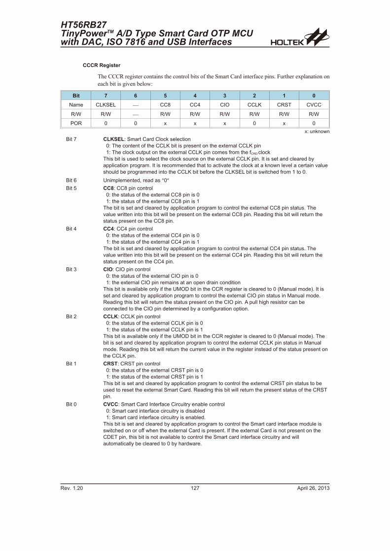
CCCR Register
The CCCR register contains the control bits of the Smart Card interface pins. Further explanation on
each bit is given below:
Bit 7 6 5 4 3 2 1 0
Name CLKSEL � CC8 CC4 CIO CCLK CRST CVCC
R/W R/W � R/W R/W R/W R/W R/W R/W
POR 0 0 x x x 0 x 0
x: unknown
Bit 7 CLKSEL: Smart Card Clock selection
0: The content of the CCLK bit is present on the external CCLK pin
1: The clock output on the external CCLK pin comes from the fCRD clock
This bit is used to select the clock source on the external CCLK pin. It is set and cleared by
application program. It is recommended that to activate the clock at a known level a certain value
should be programmed into the CCLK bit before the CLKSEL bit is switched from 1 to 0.
Bit 6 Unimplemented, read as �0�
Bit 5 CC8: CC8 pin control
0: the status of the external CC8 pin is 0
1: the status of the external CC8 pin is 1
The bit is set and cleared by application program to control the external CC8 pin status. The
value written into this bit will be present on the external CC8 pin. Reading this bit will return the
status present on the CC8 pin.
Bit 4 CC4: CC4 pin control
0: the status of the external CC4 pin is 0
1: the status of the external CC4 pin is 1
The bit is set and cleared by application program to control the external CC4 pin status. The
value written into this bit will be present on the external CC4 pin. Reading this bit will return the
status present on the CC4 pin.
Bit 3 CIO: CIO pin control
0: the status of the external CIO pin is 0
1: the external CIO pin remains at an open drain condition
This bit is available only if the UMOD bit in the CCR register is cleared to 0 (Manual mode). It is
set and cleared by application program to control the external CIO pin status in Manual mode.
Reading this bit will return the status present on the CIO pin. A pull high resistor can be
connected to the CIO pin determined by a configuration option.
Bit 2 CCLK: CCLK pin control
0: the status of the external CCLK pin is 0
1: the status of the external CCLK pin is 1
This bit is available only if the UMOD bit in the CCR register is cleared to 0 (Manual mode). The
bit is set and cleared by application program to control the external CCLK pin status in Manual
mode. Reading this bit will return the current value in the register instead of the status present on
the CCLK pin.
Bit 1 CRST: CRST pin control
0: the status of the external CRST pin is 0
1: the status of the external CRST pin is 1
This bit is set and cleared by application program to control the external CRST pin status to be
used to reset the external Smart Card. Reading this bit will return the present status of the CRST
pin.
Bit 0 CVCC: Smart Card Interface Circuitry enable control
0: Smart card interface circuitry is disabled
1: Smart card interface circuitry is enabled.
This bit is set and cleared by application program to control the Smart card interface module is
switched on or off when the external Card is present. If the external Card is not present on the
CDET pin, this bit is not available to control the Smart card interface circuitry and will
automatically be cleared to 0 by hardware.
HT56RB27TinyPowerTM A/D Type Smart Card OTP MCUwith DAC, ISO 7816 and USB Interfaces
Rev. 1.20 127 April 26, 2013

CETU Registers
The CETU registers, CETU1 and CETU0, contain the specific values determined by the formula
described in the ETU section. It also includes a control bit of the Compensation function for the ETU
time granularity. Note that the value of the ETU must be in the range of 001H to 7FFH. To obtain the
maximum ETU decimal value of 2048, a 000H value should be written into the ETU10~ETU0 bits.
Further explanation on each bit is given below:
Bit 7 6 5 4 3 2 1 0
Name COMP � � � � ETU10 ETU9 ETU8
R/W R/W � � � � R/W R/W R/W
POR 0 0 0 0 0 0 0 1
Bit 7 COMP: Compensation function enable control
0: Compensation function is disabled.
1: Compensation function is enabled.
This bit is set and cleared by application program used to control the Compensation function.
The Compensation function has been described and more details can be obtained in the ETU
section.
Bit 6~3 Unimplemented, read as �0�.
Bit 2~0 ETU10~ETU8: bit 10~8 of the ETU value
The bits are set and cleared by application program to modify the ETU values. Writing to the
CETU1 register will reload the updated value into the ETU counter.
CETU0 Register
Bit 7 6 5 4 3 2 1 0
Name ETU7 ETU6 ETU5 ETU4 ETU3 ETU2 ETU1 ETU0
R/W R/W R/W R/W R/W R/W R/W R/W R/W
POR 0 1 1 1 0 1 0 0
Bit 7~0 ETU7~ETU0: bit 7~0 of the ETU value
The bits are set and cleared by application program to modify the ETU values.
Rev. 1.20 128 April 26, 2013
HT56RB27TinyPowerTM A/D Type Smart Card OTP MCU
with DAC, ISO 7816 and USB Interfaces
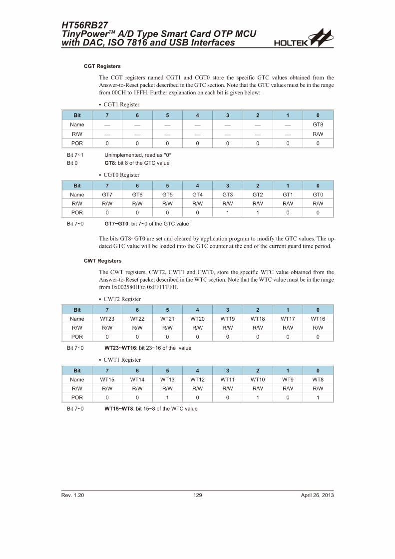
CGT Registers
The CGT registers named CGT1 and CGT0 store the specific GTC values obtained from the
Answer-to-Reset packet described in the GTC section. Note that the GTC values must be in the range
from 00CH to 1FFH. Further explanation on each bit is given below:
� CGT1 Register
Bit 7 6 5 4 3 2 1 0
Name � � � � � � � GT8
R/W � � � � � � � R/W
POR 0 0 0 0 0 0 0 0
Bit 7~1 Unimplemented, read as �0�
Bit 0 GT8: bit 8 of the GTC value
� CGT0 Register
Bit 7 6 5 4 3 2 1 0
Name GT7 GT6 GT5 GT4 GT3 GT2 GT1 GT0
R/W R/W R/W R/W R/W R/W R/W R/W R/W
POR 0 0 0 0 1 1 0 0
Bit 7~0 GT7~GT0: bit 7~0 of the GTC value
The bits GT8~GT0 are set and cleared by application program to modify the GTC values. The up-
dated GTC value will be loaded into the GTC counter at the end of the current guard time period.
CWT Registers
The CWT registers, CWT2, CWT1 and CWT0, store the specific WTC value obtained from the
Answer-to-Reset packet described in the WTC section. Note that the WTC value must be in the range
from 0x002580H to 0xFFFFFFH.
� CWT2 Register
Bit 7 6 5 4 3 2 1 0
Name WT23 WT22 WT21 WT20 WT19 WT18 WT17 WT16
R/W R/W R/W R/W R/W R/W R/W R/W R/W
POR 0 0 0 0 0 0 0 0
Bit 7~0 WT23~WT16: bit 23~16 of the value
� CWT1 Register
Bit 7 6 5 4 3 2 1 0
Name WT15 WT14 WT13 WT12 WT11 WT10 WT9 WT8
R/W R/W R/W R/W R/W R/W R/W R/W R/W
POR 0 0 1 0 0 1 0 1
Bit 7~0 WT15~WT8: bit 15~8 of the WTC value
HT56RB27TinyPowerTM A/D Type Smart Card OTP MCUwith DAC, ISO 7816 and USB Interfaces
Rev. 1.20 129 April 26, 2013
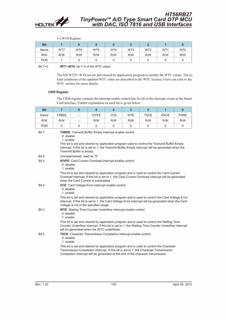
� CWT0 Register
Bit 7 6 5 4 3 2 1 0
Name WT7 WT6 WT5 WT4 WT3 WT2 WT1 WT0
R/W R/W R/W R/W R/W R/W R/W R/W R/W
POR 1 0 0 0 0 0 0 0
Bit 7~0 WT7~WT0: bit 7~0 of the WTC value
The bits WT23~WT0 are set and cleared by application program to modify the WTC values. The re-
load conditions of the updated WTC value are described in the WTC section. Users can refer to the
WTC section for more details.
CIER Register
The CIER register contains the interrupt enable control bits for all of the interrupt events in the Smart
Card interface. Further explanation on each bit is given below:
Bit 7 6 5 4 3 2 1 0
Name TXBEE � IOVFE VCE WTE TXCE RXCE PARE
R/W R/W � R/W R/W R/W R/W R/W R/W
POR 0 0 0 0 0 0 0 0
Bit 7 TXBEE: Transmit Buffer Empty interrupt enable control
0: disable
1: enable
This bit is set and cleared by application program used to control the Transmit Buffer Empty
interrupt. If this bit is set to 1, the Transmit Buffer Empty interrupt will be generated when the
Transmit Buffer is empty.
Bit 6 Unimplemented, read as �0�
Bit 5 IOVFE: Card Current Overload interrupt enable control
0: disable
1: enable
This bit is set and cleared by application program and is used to control the Card Current
Overload interrupt. If this bit is set to 1, the Card Current Overload interrupt will be generated
when the Card Current is overloaded.
Bit 4 VCE: Card Voltage Error interrupt enable control
0: disable
1: enable
This bit is set and cleared by application program and is used to control the Card Voltage Error
interrupt. If this bit is set to 1, the Card Voltage Error interrupt will be generated when the Card
Voltage is not in the specified range.
Bit 3 WTE: Waiting Time Counter Underflow interrupt enable control
0: disable
1: enable
This bit is set and cleared by application program and is used to control the Waiting Time
Counter Underflow interrupt. If this bit is set to 1, the Waiting Time Counter Underflow interrupt
will be generated when the WTC underflows.
Bit 2 TXCE: Character Transmission Completion interrupt enable control
0: disable
1: enable
This bit is set and cleared by application program and is used to control the Character
Transmission Completion interrupt. If this bit is set to 1, the Character Transmission
Completion interrupt will be generated at the end of the character transmission.
Rev. 1.20 130 April 26, 2013
HT56RB27TinyPowerTM A/D Type Smart Card OTP MCU
with DAC, ISO 7816 and USB Interfaces
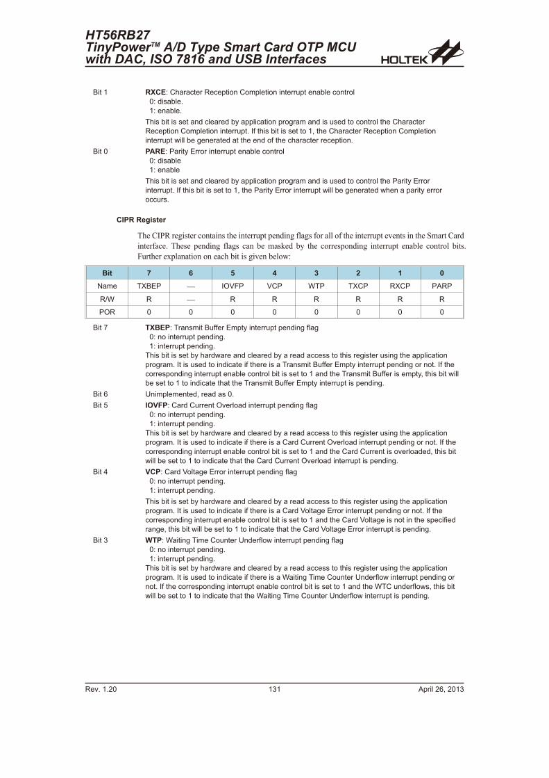
Bit 1 RXCE: Character Reception Completion interrupt enable control
0: disable.
1: enable.
This bit is set and cleared by application program and is used to control the Character
Reception Completion interrupt. If this bit is set to 1, the Character Reception Completion
interrupt will be generated at the end of the character reception.
Bit 0 PARE: Parity Error interrupt enable control
0: disable
1: enable
This bit is set and cleared by application program and is used to control the Parity Error
interrupt. If this bit is set to 1, the Parity Error interrupt will be generated when a parity error
occurs.
CIPR Register
The CIPR register contains the interrupt pending flags for all of the interrupt events in the Smart Card
interface. These pending flags can be masked by the corresponding interrupt enable control bits.
Further explanation on each bit is given below:
Bit 7 6 5 4 3 2 1 0
Name TXBEP � IOVFP VCP WTP TXCP RXCP PARP
R/W R � R R R R R R
POR 0 0 0 0 0 0 0 0
Bit 7 TXBEP: Transmit Buffer Empty interrupt pending flag
0: no interrupt pending.
1: interrupt pending.
This bit is set by hardware and cleared by a read access to this register using the application
program. It is used to indicate if there is a Transmit Buffer Empty interrupt pending or not. If the
corresponding interrupt enable control bit is set to 1 and the Transmit Buffer is empty, this bit will
be set to 1 to indicate that the Transmit Buffer Empty interrupt is pending.
Bit 6 Unimplemented, read as 0.
Bit 5 IOVFP: Card Current Overload interrupt pending flag
0: no interrupt pending.
1: interrupt pending.
This bit is set by hardware and cleared by a read access to this register using the application
program. It is used to indicate if there is a Card Current Overload interrupt pending or not. If the
corresponding interrupt enable control bit is set to 1 and the Card Current is overloaded, this bit
will be set to 1 to indicate that the Card Current Overload interrupt is pending.
Bit 4 VCP: Card Voltage Error interrupt pending flag
0: no interrupt pending.
1: interrupt pending.
This bit is set by hardware and cleared by a read access to this register using the application
program. It is used to indicate if there is a Card Voltage Error interrupt pending or not. If the
corresponding interrupt enable control bit is set to 1 and the Card Voltage is not in the specified
range, this bit will be set to 1 to indicate that the Card Voltage Error interrupt is pending.
Bit 3 WTP: Waiting Time Counter Underflow interrupt pending flag
0: no interrupt pending.
1: interrupt pending.
This bit is set by hardware and cleared by a read access to this register using the application
program. It is used to indicate if there is a Waiting Time Counter Underflow interrupt pending or
not. If the corresponding interrupt enable control bit is set to 1 and the WTC underflows, this bit
will be set to 1 to indicate that the Waiting Time Counter Underflow interrupt is pending.
HT56RB27TinyPowerTM A/D Type Smart Card OTP MCUwith DAC, ISO 7816 and USB Interfaces
Rev. 1.20 131 April 26, 2013
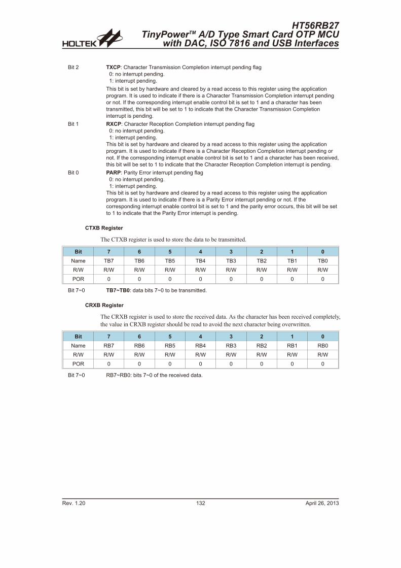
Bit 2 TXCP: Character Transmission Completion interrupt pending flag
0: no interrupt pending.
1: interrupt pending.
This bit is set by hardware and cleared by a read access to this register using the application
program. It is used to indicate if there is a Character Transmission Completion interrupt pending
or not. If the corresponding interrupt enable control bit is set to 1 and a character has been
transmitted, this bit will be set to 1 to indicate that the Character Transmission Completion
interrupt is pending.
Bit 1 RXCP: Character Reception Completion interrupt pending flag
0: no interrupt pending.
1: interrupt pending.
This bit is set by hardware and cleared by a read access to this register using the application
program. It is used to indicate if there is a Character Reception Completion interrupt pending or
not. If the corresponding interrupt enable control bit is set to 1 and a character has been received,
this bit will be set to 1 to indicate that the Character Reception Completion interrupt is pending.
Bit 0 PARP: Parity Error interrupt pending flag
0: no interrupt pending.
1: interrupt pending.
This bit is set by hardware and cleared by a read access to this register using the application
program. It is used to indicate if there is a Parity Error interrupt pending or not. If the
corresponding interrupt enable control bit is set to 1 and the parity error occurs, this bit will be set
to 1 to indicate that the Parity Error interrupt is pending.
CTXB Register
The CTXB register is used to store the data to be transmitted.
Bit 7 6 5 4 3 2 1 0
Name TB7 TB6 TB5 TB4 TB3 TB2 TB1 TB0
R/W R/W R/W R/W R/W R/W R/W R/W R/W
POR 0 0 0 0 0 0 0 0
Bit 7~0 TB7~TB0: data bits 7~0 to be transmitted.
CRXB Register
The CRXB register is used to store the received data. As the character has been received completely,
the value in CRXB register should be read to avoid the next character being overwritten.
Bit 7 6 5 4 3 2 1 0
Name RB7 RB6 RB5 RB4 RB3 RB2 RB1 RB0
R/W R/W R/W R/W R/W R/W R/W R/W R/W
POR 0 0 0 0 0 0 0 0
Bit 7~0 RB7~RB0: bits 7~0 of the received data.
Rev. 1.20 132 April 26, 2013
HT56RB27TinyPowerTM A/D Type Smart Card OTP MCU
with DAC, ISO 7816 and USB Interfaces
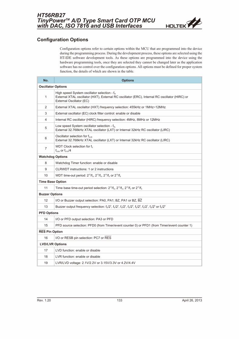
Configuration Options
Configuration options refer to certain options within the MCU that are programmed into the device
during the programming process. During the development process, these options are selected using the
HT-IDE software development tools. As these options are programmed into the device using the
hardware programming tools, once they are selected they cannot be changed later as the application
software has no control over the configuration options. All options must be defined for proper system
function, the details of which are shown in the table.
No. Options
Oscillator Options
1
High speed System oscillator selection - fM
External XTAL oscillator (HXT), External RC oscillator (ERC), Internal RC oscillator (HIRC) or
External Oscillator (EC)
2 External XTAL oscilaltor (HXT) frequency selection: 455kHz or 1MHz~12MHz
3 External oscillator (EC) clock filter control: enable or disable
4 Internal RC oscillator (HIRC) frequency selection: 4MHz, 8MHz or 12MHz
5Low speed System oscillator selection - fSL
External 32.768kHz XTAL oscillator (LXT) or Internal 32kHz RC oscillator (LIRC)
6Oscillator selection for fSUB
External 32.768kHz XTAL oscillator (LXT) or Internal 32kHz RC oscillator (LIRC)
7WDT Clock selection for fS
fSUB or fSYS/4
Watchdog Options
8 Watchdog Timer function: enable or disable
9 CLRWDT instructions: 1 or 2 instructions
10 WDT time-out period: 212/fS, 213/fS, 214/fS or 215/fS
Time Base Option
11 Time base time-out period selection: 212/fS, 213/fS, 214/fS or 215/fS
Buzzer Options
12 I/O or Buzzer output selection: PA0, PA1; BZ, PA1 or BZ, BZ
13 Buzzer output frequency selection: fS/22, fS/2
3, fS/24, fS/2
5, fS/26, fS/2
7, fS/28 or fS/2
9
PFD Options
14 I/O or PFD output selection: PA3 or PFD
15 PFD source selection: PFD0 (from Timer/event counter 0) or PFD1 (from Timer/event counter 1)
RES Pin Option
16 I/O or RESB pin selection: PC7 or RES
LVD/LVR Options
17 LVD function: enable or disable
18 LVR function: enable or disable
19 LVR/LVD voltage: 2.1V/2.2V or 3.15V/3.3V or 4.2V/4.4V
HT56RB27TinyPowerTM A/D Type Smart Card OTP MCUwith DAC, ISO 7816 and USB Interfaces
Rev. 1.20 133 April 26, 2013
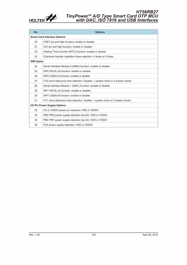
No. Options
Smart Card Interface Options
20 CDET pin pull high function: enable or disable
21 CIO pin pull high function: enable or disable
22 Waiting Time Counter (WTC) function: enable or disable
23 Character transfer repetition times selection: 4 times or 5 times
SIM Option
24 Serial Interface Module 0 (SIM0) function: enable or disable
25 SPI0 WCOL bit function: enable or disable
26 SPI0 CSEN bit function: enable or disable
27 I2C0 clock debounce time selection: Disable, 1 system clock or 2 system clocks
28 Serial Interface Module 1 (SIM1) function: enable or disable
29 SPI1 WCOL bit function: enable or disable
30 SPI1 CSEN bit function: enable or disable
31 I2C1 clock debounce time selection: disable, 1 system clock or 2 system clocks
I/O Pin Power Supply Options
32 I/O or VDDIO power pin selection: PB3 or VDDIO
33 PB0~PB2 power supply selection (by bit): VDD or VDDIO
34 PB4~PB7 power supply selection (by bit): VDD or VDDIO
35 PC4 power supply selection: VDD or VDDIO
Rev. 1.20 134 April 26, 2013
HT56RB27TinyPowerTM A/D Type Smart Card OTP MCU
with DAC, ISO 7816 and USB Interfaces

Application Circuits
Note: �*� Recommended component for added ESD protection.
�**� Recommended component in environments where power line noise is significant.
HT56RB27TinyPowerTM A/D Type Smart Card OTP MCUwith DAC, ISO 7816 and USB Interfaces
Rev. 1.20 135 April 26, 2013
� � � # � + � �
� � # #
� # = � � 5
� # #
7 � � � �
� � �
, � � � � & � �
7 � � G � � �
� 7 " � G
� 7 7 " �
& 7 7 � J
7 � 7 � � � J J
� 4 ' � ' 6
� # �� � # #� � + B� �
� � � �� � ' 0 � � � 6
# � � ! � �� � ! ;
� � � � �
� � ' G � � *
� 8 7 G � 8 5
� , 7 = , 4 7 G � , 5 = , 4 5
� � 7 = # � �
� � � = # � �
# � �� � ! � � �
� � � = # � &
� � & = # � '
# � �� � ! � � �
# � � � � � � � � � ! �# � � � �
# � � � � � � � � � ! �# � � � �
� � � �
� 7 7 � 2 = � �
' � 5 � �
� �� 4
> # 8
� & & & & �
& & �
' 5 ( �' 5 ( �
� � ) " �
7 � � � �
Instruction Set
Introduction
Central to the successful operation of any microcontroller is its instruction set, which is a set of
program instruction codes that directs the microcontroller to perform certain operations. In the case of
Holtek microcontrollers, a comprehensive and flexible set of over 60 instructions is provided to enable
programmers to implement their application with the minimum of programming overheads.
For easier understanding of the various instruction codes, they have been subdivided into several
functional groupings.
Instruction Timing
Most instructions are implemented within one instruction cycle. The exceptions to this are branch, call,
or table read instructions where two instruction cycles are required. One instruction cycle is equal to 4
system clock cycles, therefore in the case of an 8MHz system oscillator, most instructions would be
implemented within 0.5�s and branch or call instructions would be implemented within 1�s. Although
instructions which require one more cycle to implement are generally limited to the JMP, CALL, RET,
RETI and table read instructions, it is important to realize that any other instructions which involve
manipulation of the Program Counter Low register or PCL will also take one more cycle to implement.
As instructions which change the contents of the PCL will imply a direct jump to that new address, one
more cycle will be required. Examples of such instructions would be �CLR PCL� or �MOV PCL, A�.
For the case of skip instructions, it must be noted that if the result of the comparison involves a skip
operation then this will also take one more cycle, if no skip is involved then only one cycle is required.
Moving and Transferring Data
The transfer of data within the microcontroller program is one of the most frequently used operations.
Making use of three kinds of MOV instructions, data can be transferred from registers to the
Accumulator and vice-versa as well as being able to move specific immediate data directly into the
Accumulator. One of the most important data transfer applications is to receive data from the input
ports and transfer data to the output ports.
Arithmetic Operations
The ability to perform certain arithmetic operations and data manipulation is a necessary feature of
most microcontroller applications. Within the Holtek microcontroller instruction set are a range of add
and subtract instruction mnemonics to enable the necessary arithmetic to be carried out. Care must be
taken to ensure correct handling of carry and borrow data when results exceed 255 for addition and less
than 0 for subtraction. The increment and decrement instructions INC, INCA, DEC and DECA
provide a simple means of increasing or decreasing by a value of one of the values in the destination
specified.
Logical and Rotate Operations
The standard logical operations such as AND, OR, XOR and CPL all have their own instruction within
the Holtek microcontroller instruction set. As with the case of most instructions involving data
manipulation, data must pass through the Accumulator which may involve additional programming
steps. In all logical data operations, the zero flag may be set if the result of the operation is zero.
Another form of logical data manipulation comes from the rotate instructions such as RR, RL, RRC
and RLC which provide a simple means of rotating one bit right or left. Different rotate instructions
exist depending on program requirements. Rotate instructions are useful for serial port programming
applications where data can be rotated from an internal register into the Carry bit from where it can be
examined and the necessary serial bit set high or low. Another application where rotate data operations
are used is to implement multiplication and division calculations.
Rev. 1.20 136 April 26, 2013
HT56RB27TinyPowerTM A/D Type Smart Card OTP MCU
with DAC, ISO 7816 and USB Interfaces
Branches and Control Transfer
Program branching takes the form of either jumps to specified locations using the JMP instruction or to
a subroutine using the CALL instruction. They differ in the sense that in the case of a subroutine call,
the program must return to the instruction immediately when the subroutine has been carried out. This
is done by placing a return instruction RET in the subroutine which will cause the program to jump
back to the address right after the CALL instruction. In the case of a JMP instruction, the program
simply jumps to the desired location. There is no requirement to jump back to the original jumping off
point as in the case of the CALL instruction. One special and extremely useful set of branch
instructions are the conditional branches. Here a decision is first made regarding the condition of a
certain data memory or individual bits. Depending upon the conditions, the program will continue with
the next instruction or skip over it and jump to the following instruction. These instructions are the key
to decision making and branching within the program perhaps determined by the condition of certain
input switches or by the condition of internal data bits.
Bit Operations
The ability to provide single bit operations on Data Memory is an extremely flexible feature of all
Holtek microcontrollers. This feature is especially useful for output port bit programming where
individual bits or port pins can be directly set high or low using either the �SET [m].i� or �CLR [m].i�
instructions respectively. The feature removes the need for programmers to first read the 8-bit output
port, manipulate the input data to ensure that other bits are not changed and then output the port with
the correct new data. This read-modify-write process is taken care of automatically when these bit
operation instructions are used.
Table Read Operations
Data storage is normally implemented by using registers. However, when working with large amounts
of fixed data, the volume involved often makes it inconvenient to store the fixed data in the Data
Memory. To overcome this problem, Holtek microcontrollers allow an area of Program Memory to be
setup as a table where data can be directly stored. A set of easy to use instructions provides the means
by which this fixed data can be referenced and retrieved from the Program Memory.
Other Operations
In addition to the above functional instructions, a range of other instructions also exist such as the
�HALT� instruction for Power-down operations and instructions to control the operation of the
Watchdog Timer for reliable program operations under extreme electric or electromagnetic
environments. For their relevant operations, refer to the functional related sections.
HT56RB27TinyPowerTM A/D Type Smart Card OTP MCUwith DAC, ISO 7816 and USB Interfaces
Rev. 1.20 137 April 26, 2013
Instruction Set Summary
The following table depicts a summary of the instruction set categorised according to function and can
be consulted as a basic instruction reference using the following listed conventions.
Table conventions:
x: Bits immediate data
m: Data Memory address
A: Accumulator
i: 0~7 number of bits
addr: Program memory address
Mnemonic Description Cycles Flag Affected
Arithmetic
ADD A,[m]
ADDM A,[m]
ADD A,x
ADC A,[m]
ADCM A,[m]
SUB A,x
SUB A,[m]
SUBM A,[m]
SBC A,[m]
SBCM A,[m]
DAA [m]
Add Data Memory to ACC
Add ACC to Data Memory
Add immediate data to ACC
Add Data Memory to ACC with Carry
Add ACC to Data memory with Carry
Subtract immediate data from the ACC
Subtract Data Memory from ACC
Subtract Data Memory from ACC with result in Data Memory
Subtract Data Memory from ACC with Carry
Subtract Data Memory from ACC with Carry, result in Data Memory
Decimal adjust ACC for Addition with result in Data Memory
1
1Note
1
1
1Note
1
1
1Note
1
1Note
1Note
Z, C, AC, OV
Z, C, AC, OV
Z, C, AC, OV
Z, C, AC, OV
Z, C, AC, OV
Z, C, AC, OV
Z, C, AC, OV
Z, C, AC, OV
Z, C, AC, OV
Z, C, AC, OV
C
Logic Operation
AND A,[m]
OR A,[m]
XOR A,[m]
ANDM A,[m]
ORM A,[m]
XORM A,[m]
AND A,x
OR A,x
XOR A,x
CPL [m]
CPLA [m]
Logical AND Data Memory to ACC
Logical OR Data Memory to ACC
Logical XOR Data Memory to ACC
Logical AND ACC to Data Memory
Logical OR ACC to Data Memory
Logical XOR ACC to Data Memory
Logical AND immediate Data to ACC
Logical OR immediate Data to ACC
Logical XOR immediate Data to ACC
Complement Data Memory
Complement Data Memory with result in ACC
1
1
1
1Note
1Note
1Note
1
1
1
1Note
1
Z
Z
Z
Z
Z
Z
Z
Z
Z
Z
Z
Increment & Decrement
INCA [m]
INC [m]
DECA [m]
DEC [m]
Increment Data Memory with result in ACC
Increment Data Memory
Decrement Data Memory with result in ACC
Decrement Data Memory
1
1Note
1
1Note
Z
Z
Z
Z
Rotate
RRA [m]
RR [m]
RRCA [m]
RRC [m]
RLA [m]
RL [m]
RLCA [m]
RLC [m]
Rotate Data Memory right with result in ACC
Rotate Data Memory right
Rotate Data Memory right through Carry with result in ACC
Rotate Data Memory right through Carry
Rotate Data Memory left with result in ACC
Rotate Data Memory left
Rotate Data Memory left through Carry with result in ACC
Rotate Data Memory left through Carry
1
1Note
1
1Note
1
1Note
1
1Note
None
None
C
C
None
None
C
C
Data Move
MOV A,[m]
MOV [m],A
MOV A,x
Move Data Memory to ACC
Move ACC to Data Memory
Move immediate data to ACC
1
1Note
1
None
None
None
Rev. 1.20 138 April 26, 2013
HT56RB27TinyPowerTM A/D Type Smart Card OTP MCU
with DAC, ISO 7816 and USB Interfaces
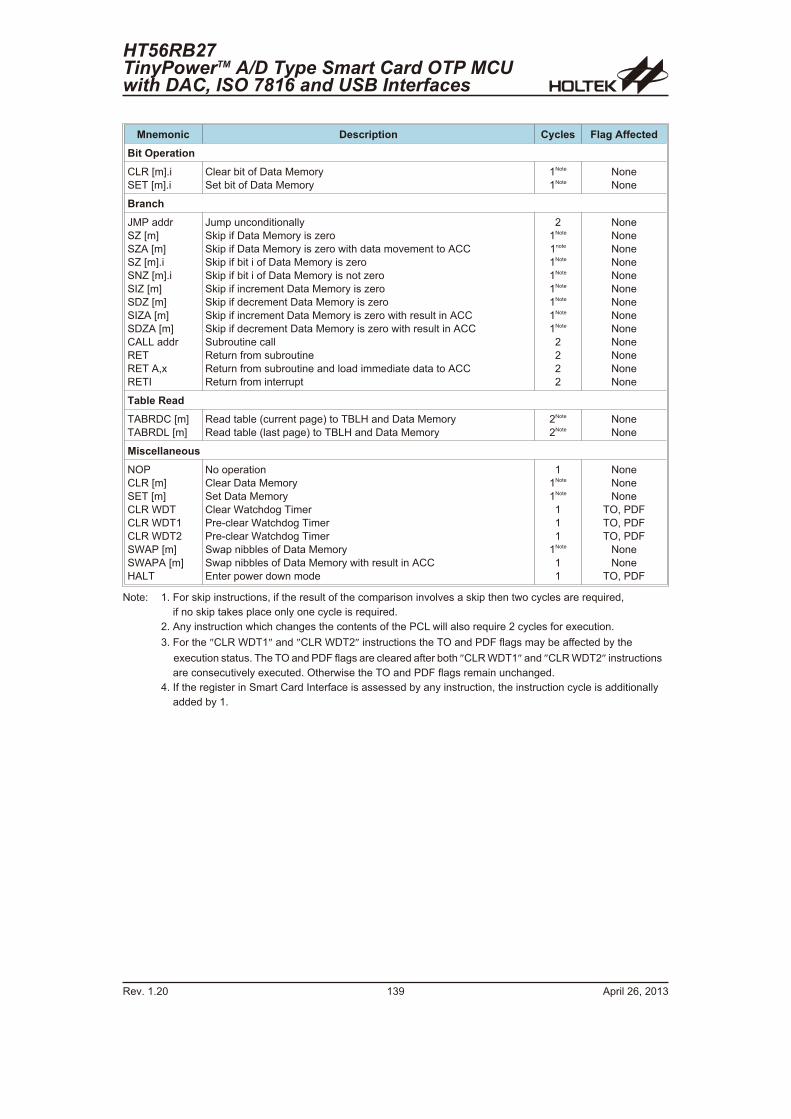
Mnemonic Description Cycles Flag Affected
Bit Operation
CLR [m].i
SET [m].i
Clear bit of Data Memory
Set bit of Data Memory
1Note
1Note
None
None
Branch
JMP addr
SZ [m]
SZA [m]
SZ [m].i
SNZ [m].i
SIZ [m]
SDZ [m]
SIZA [m]
SDZA [m]
CALL addr
RET
RET A,x
RETI
Jump unconditionally
Skip if Data Memory is zero
Skip if Data Memory is zero with data movement to ACC
Skip if bit i of Data Memory is zero
Skip if bit i of Data Memory is not zero
Skip if increment Data Memory is zero
Skip if decrement Data Memory is zero
Skip if increment Data Memory is zero with result in ACC
Skip if decrement Data Memory is zero with result in ACC
Subroutine call
Return from subroutine
Return from subroutine and load immediate data to ACC
Return from interrupt
2
1Note
1note
1Note
1Note
1Note
1Note
1Note
1Note
2
2
2
2
None
None
None
None
None
None
None
None
None
None
None
None
None
Table Read
TABRDC [m]
TABRDL [m]
Read table (current page) to TBLH and Data Memory
Read table (last page) to TBLH and Data Memory
2Note
2Note
None
None
Miscellaneous
NOP
CLR [m]
SET [m]
CLR WDT
CLR WDT1
CLR WDT2
SWAP [m]
SWAPA [m]
HALT
No operation
Clear Data Memory
Set Data Memory
Clear Watchdog Timer
Pre-clear Watchdog Timer
Pre-clear Watchdog Timer
Swap nibbles of Data Memory
Swap nibbles of Data Memory with result in ACC
Enter power down mode
1
1Note
1Note
1
1
1
1Note
1
1
None
None
None
TO, PDF
TO, PDF
TO, PDF
None
None
TO, PDF
Note: 1. For skip instructions, if the result of the comparison involves a skip then two cycles are required,
if no skip takes place only one cycle is required.
2. Any instruction which changes the contents of the PCL will also require 2 cycles for execution.
3. For the �CLR WDT1� and �CLR WDT2� instructions the TO and PDF flags may be affected by the
execution status. The TO and PDF flags are cleared after both �CLR WDT1� and �CLR WDT2� instructions
are consecutively executed. Otherwise the TO and PDF flags remain unchanged.
4. If the register in Smart Card Interface is assessed by any instruction, the instruction cycle is additionally
added by 1.
HT56RB27TinyPowerTM A/D Type Smart Card OTP MCUwith DAC, ISO 7816 and USB Interfaces
Rev. 1.20 139 April 26, 2013
Instruction Definition
ADC A,[m] Add Data Memory to ACC with Carry
Description The contents of the specified Data Memory, Accumulator and the carry flag are added.
The result is stored in the Accumulator.
Operation ACC � ACC + [m] + C
Affected flag(s) OV, Z, AC, C
ADCM A,[m] Add ACC to Data Memory with Carry
Description The contents of the specified Data Memory, Accumulator and the carry flag are added.
The result is stored in the specified Data Memory.
Operation [m] � ACC + [m] + C
Affected flag(s) OV, Z, AC, C
ADD A,[m] Add Data Memory to ACC
Description The contents of the specified Data Memory and the Accumulator are added. The result is
stored in the Accumulator.
Operation ACC � ACC + [m]
Affected flag(s) OV, Z, AC, C
ADD A,x Add immediate data to ACC
Description The contents of the Accumulator and the specified immediate data are added. The result
is stored in the Accumulator.
Operation ACC � ACC + x
Affected flag(s) OV, Z, AC, C
ADDM A,[m] Add ACC to Data Memory
Description The contents of the specified Data Memory and the Accumulator are added. The result is
stored in the specified Data Memory.
Operation [m] � ACC + [m]
Affected flag(s) OV, Z, AC, C
AND A,[m] Logical AND Data Memory to ACC
Description Data in the Accumulator and the specified Data Memory perform a bitwise logical AND
operation. The result is stored in the Accumulator.
Operation ACC � ACC �AND� [m]
Affected flag(s) Z
AND A,x Logical AND immediate data to ACC
Description Data in the Accumulator and the specified immediate data perform a bitwise logical
AND operation. The result is stored in the Accumulator.
Operation ACC � ACC �AND� x
Affected flag(s) Z
ANDM A,[m] Logical AND ACC to Data Memory
Description Data in the specified Data Memory and the Accumulator perform a bitwise logical AND
operation. The result is stored in the Data Memory.
Operation [m] � ACC �AND� [m]
Affected flag(s) Z
Rev. 1.20 140 April 26, 2013
HT56RB27TinyPowerTM A/D Type Smart Card OTP MCU
with DAC, ISO 7816 and USB Interfaces
CALL addr Subroutine call
Description Unconditionally calls a subroutine at the specified address. The Program Counter then
increments by 1 to obtain the address of the next instruction which is then pushed onto
the stack. The specified address is then loaded and the program continues execution
from this new address. As this instruction requires an additional operation, it is a two cy-
cle instruction.
Operation Stack � Program Counter + 1
Program Counter � addr
Affected flag(s) None
CLR [m] Clear Data Memory
Description Each bit of the specified Data Memory is cleared to 0.
Operation [m] � 00H
Affected flag(s) None
CLR [m].i Clear bit of Data Memory
Description Bit i of the specified Data Memory is cleared to 0.
Operation [m].i � 0
Affected flag(s) None
CLR WDT Clear Watchdog Timer
Description The TO, PDF flags and the WDT are all cleared.
Operation WDT cleared
TO � 0
PDF � 0
Affected flag(s) TO, PDF
CLR WDT1 Pre-clear Watchdog Timer
Description The TO, PDF flags and the WDT are all cleared. Note that this instruction works in con-
junction with CLR WDT2 and must be executed alternately with CLR WDT2 to have ef-
fect. Repetitively executing this instruction without alternately executing CLR WDT2
will have no effect.
Operation WDT cleared
TO � 0
PDF � 0
Affected flag(s) TO, PDF
CLR WDT2 Pre-clear Watchdog Timer
Description The TO, PDF flags and the WDT are all cleared. Note that this instruction works in con-
junction with CLR WDT1 and must be executed alternately with CLR WDT1 to have ef-
fect. Repetitively executing this instruction without alternately executing CLR WDT1
will have no effect.
Operation WDT cleared
TO � 0
PDF � 0
Affected flag(s) TO, PDF
HT56RB27TinyPowerTM A/D Type Smart Card OTP MCUwith DAC, ISO 7816 and USB Interfaces
Rev. 1.20 141 April 26, 2013
CPL [m] Complement Data Memory
Description Each bit of the specified Data Memory is logically complemented (1�s complement).
Bits which previously contained a 1 are changed to 0 and vice versa.
Operation [m] � [m]
Affected flag(s) Z
CPLA [m] Complement Data Memory with result in ACC
Description Each bit of the specified Data Memory is logically complemented (1�s complement).
Bits which previously contained a 1 are changed to 0 and vice versa. The complemented
result is stored in the Accumulator and the contents of the Data Memory remain un-
changed.
Operation ACC � [m]
Affected flag(s) Z
DAA [m] Decimal-Adjust ACC for addition with result in Data Memory
Description Convert the contents of the Accumulator value to a BCD ( Binary Coded Decimal) value
resulting from the previous addition of two BCD variables. If the low nibble is greater
than 9 or if AC flag is set, then a value of 6 will be added to the low nibble. Otherwise the
low nibble remains unchanged. If the high nibble is greater than 9 or if the C flag is set,
then a value of 6 will be added to the high nibble. Essentially, the decimal conversion is
performed by adding 00H, 06H, 60H or 66H depending on the Accumulator and flag
conditions. Only the C flag may be affected by this instruction which indicates that if the
original BCD sum is greater than 100, it allows multiple precision decimal addition.
Operation [m] � ACC + 00H or
[m] � ACC + 06H or
[m] � ACC + 60H or
[m] � ACC + 66H
Affected flag(s) C
DEC [m] Decrement Data Memory
Description Data in the specified Data Memory is decremented by 1.
Operation [m] � [m] � 1
Affected flag(s) Z
DECA [m] Decrement Data Memory with result in ACC
Description Data in the specified Data Memory is decremented by 1. The result is stored in the Accu-
mulator. The contents of the Data Memory remain unchanged.
Operation ACC � [m] � 1
Affected flag(s) Z
HALT Enter power down mode
Description This instruction stops the program execution and turns off the system clock. The con-
tents of the Data Memory and registers are retained. The WDT and prescaler are cleared.
The power down flag PDF is set and the WDT time-out flag TO is cleared.
Operation TO � 0
PDF � 1
Affected flag(s) TO, PDF
Rev. 1.20 142 April 26, 2013
HT56RB27TinyPowerTM A/D Type Smart Card OTP MCU
with DAC, ISO 7816 and USB Interfaces
INC [m] Increment Data Memory
Description Data in the specified Data Memory is incremented by 1.
Operation [m] � [m] + 1
Affected flag(s) Z
INCA [m] Increment Data Memory with result in ACC
Description Data in the specified Data Memory is incremented by 1. The result is stored in the Accu-
mulator. The contents of the Data Memory remain unchanged.
Operation ACC � [m] + 1
Affected flag(s) Z
JMP addr Jump unconditionally
Description The contents of the Program Counter are replaced with the specified address. Program
execution then continues from this new address. As this requires the insertion of a
dummy instruction while the new address is loaded, it is a two cycle instruction.
Operation Program Counter � addr
Affected flag(s) None
MOV A,[m] Move Data Memory to ACC
Description The contents of the specified Data Memory are copied to the Accumulator.
Operation ACC � [m]
Affected flag(s) None
MOV A,x Move immediate data to ACC
Description The immediate data specified is loaded into the Accumulator.
Operation ACC � x
Affected flag(s) None
MOV [m],A Move ACC to Data Memory
Description The contents of the Accumulator are copied to the specified Data Memory.
Operation [m] � ACC
Affected flag(s) None
NOP No operation
Description No operation is performed. Execution continues with the next instruction.
Operation No operation
Affected flag(s) None
OR A,[m] Logical OR Data Memory to ACC
Description Data in the Accumulator and the specified Data Memory perform a bitwise logical OR
operation. The result is stored in the Accumulator.
Operation ACC � ACC �OR� [m]
Affected flag(s) Z
HT56RB27TinyPowerTM A/D Type Smart Card OTP MCUwith DAC, ISO 7816 and USB Interfaces
Rev. 1.20 143 April 26, 2013
OR A,x Logical OR immediate data to ACC
Description Data in the Accumulator and the specified immediate data perform a bitwise logical OR
operation. The result is stored in the Accumulator.
Operation ACC � ACC �OR� x
Affected flag(s) Z
ORM A,[m] Logical OR ACC to Data Memory
Description Data in the specified Data Memory and the Accumulator perform a bitwise logical OR
operation. The result is stored in the Data Memory.
Operation [m] � ACC �OR� [m]
Affected flag(s) Z
RET Return from subroutine
Description The Program Counter is restored from the stack. Program execution continues at the re-
stored address.
Operation Program Counter � Stack
Affected flag(s) None
RET A,x Return from subroutine and load immediate data to ACC
Description The Program Counter is restored from the stack and the Accumulator loaded with the
specified immediate data. Program execution continues at the restored address.
Operation Program Counter � Stack
ACC � x
Affected flag(s) None
RETI Return from interrupt
Description The Program Counter is restored from the stack and the interrupts are re-enabled by set-
ting the EMI bit. EMI is the master interrupt global enable bit. If an interrupt was pend-
ing when the RETI instruction is executed, the pending Interrupt routine will be
processed before returning to the main program.
Operation Program Counter � Stack
EMI � 1
Affected flag(s) None
RL [m] Rotate Data Memory left
Description The contents of the specified Data Memory are rotated left by 1 bit with bit 7 rotated into
bit 0.
Operation [m].(i+1) � [m].i; (i = 0~6)
[m].0 � [m].7
Affected flag(s) None
RLA [m] Rotate Data Memory left with result in ACC
Description The contents of the specified Data Memory are rotated left by 1 bit with bit 7 rotated into
bit 0. The rotated result is stored in the Accumulator and the contents of the Data Mem-
ory remain unchanged.
Operation ACC.(i+1) � [m].i; (i = 0~6)
ACC.0 � [m].7
Affected flag(s) None
Rev. 1.20 144 April 26, 2013
HT56RB27TinyPowerTM A/D Type Smart Card OTP MCU
with DAC, ISO 7816 and USB Interfaces
RLC [m] Rotate Data Memory left through Carry
Description The contents of the specified Data Memory and the carry flag are rotated left by 1 bit. Bit
7 replaces the Carry bit and the original carry flag is rotated into bit 0.
Operation [m].(i+1) � [m].i; (i = 0~6)
[m].0 � C
C � [m].7
Affected flag(s) C
RLCA [m] Rotate Data Memory left through Carry with result in ACC
Description Data in the specified Data Memory and the carry flag are rotated left by 1 bit. Bit 7 re-
places the Carry bit and the original carry flag is rotated into the bit 0. The rotated result
is stored in the Accumulator and the contents of the Data Memory remain unchanged.
Operation ACC.(i+1) � [m].i; (i = 0~6)
ACC.0 � C
C � [m].7
Affected flag(s) C
RR [m] Rotate Data Memory right
Description The contents of the specified Data Memory are rotated right by 1 bit with bit 0 rotated
into bit 7.
Operation [m].i � [m].(i+1); (i = 0~6)
[m].7 � [m].0
Affected flag(s) None
RRA [m] Rotate Data Memory right with result in ACC
Description Data in the specified Data Memory and the carry flag are rotated right by 1 bit with bit 0
rotated into bit 7. The rotated result is stored in the Accumulator and the contents of the
Data Memory remain unchanged.
Operation ACC.i � [m].(i+1); (i = 0~6)
ACC.7 � [m].0
Affected flag(s) None
RRC [m] Rotate Data Memory right through Carry
Description The contents of the specified Data Memory and the carry flag are rotated right by 1 bit.
Bit 0 replaces the Carry bit and the original carry flag is rotated into bit 7.
Operation [m].i � [m].(i+1); (i = 0~6)
[m].7 � C
C � [m].0
Affected flag(s) C
RRCA [m] Rotate Data Memory right through Carry with result in ACC
Description Data in the specified Data Memory and the carry flag are rotated right by 1 bit. Bit 0 re-
places the Carry bit and the original carry flag is rotated into bit 7. The rotated result is
stored in the Accumulator and the contents of the Data Memory remain unchanged.
Operation ACC.i � [m].(i+1); (i = 0~6)
ACC.7 � C
C � [m].0
Affected flag(s) C
HT56RB27TinyPowerTM A/D Type Smart Card OTP MCUwith DAC, ISO 7816 and USB Interfaces
Rev. 1.20 145 April 26, 2013
SBC A,[m] Subtract Data Memory from ACC with Carry
Description The contents of the specified Data Memory and the complement of the carry flag are
subtracted from the Accumulator. The result is stored in the Accumulator. Note that if
the result of subtraction is negative, the C flag will be cleared to 0, otherwise if the result
is positive or zero, the C flag will be set to 1.
Operation ACC � ACC � [m] � C
Affected flag(s) OV, Z, AC, C
SBCM A,[m] Subtract Data Memory from ACC with Carry and result in Data Memory
Description The contents of the specified Data Memory and the complement of the carry flag are
subtracted from the Accumulator. The result is stored in the Data Memory. Note that if
the result of subtraction is negative, the C flag will be cleared to 0, otherwise if the result
is positive or zero, the C flag will be set to 1.
Operation [m] � ACC � [m] � C
Affected flag(s) OV, Z, AC, C
SDZ [m] Skip if decrement Data Memory is 0
Description The contents of the specified Data Memory are first decremented by 1. If the result is 0
the following instruction is skipped. As this requires the insertion of a dummy instruc-
tion while the next instruction is fetched, it is a two cycle instruction. If the result is not 0
the program proceeds with the following instruction.
Operation [m] � [m] � 1
Skip if [m] = 0
Affected flag(s) None
SDZA [m] Skip if decrement Data Memory is zero with result in ACC
Description The contents of the specified Data Memory are first decremented by 1. If the result is 0,
the following instruction is skipped. The result is stored in the Accumulator but the spec-
ified Data Memory contents remain unchanged. As this requires the insertion of a
dummy instruction while the next instruction is fetched, it is a two cycle instruction. If
the result is not 0, the program proceeds with the following instruction.
Operation ACC � [m] � 1
Skip if ACC = 0
Affected flag(s) None
SET [m] Set Data Memory
Description Each bit of the specified Data Memory is set to 1.
Operation [m] � FFH
Affected flag(s) None
SET [m].i Set bit of Data Memory
Description Bit i of the specified Data Memory is set to 1.
Operation [m].i � 1
Affected flag(s) None
Rev. 1.20 146 April 26, 2013
HT56RB27TinyPowerTM A/D Type Smart Card OTP MCU
with DAC, ISO 7816 and USB Interfaces
SIZ [m] Skip if increment Data Memory is 0
Description The contents of the specified Data Memory are first incremented by 1. If the result is 0,
the following instruction is skipped. As this requires the insertion of a dummy instruc-
tion while the next instruction is fetched, it is a two cycle instruction. If the result is not 0
the program proceeds with the following instruction.
Operation [m] � [m] + 1
Skip if [m] = 0
Affected flag(s) None
SIZA [m] Skip if increment Data Memory is zero with result in ACC
Description The contents of the specified Data Memory are first incremented by 1. If the result is 0,
the following instruction is skipped. The result is stored in the Accumulator but the spec-
ified Data Memory contents remain unchanged. As this requires the insertion of a
dummy instruction while the next instruction is fetched, it is a two cycle instruction. If
the result is not 0 the program proceeds with the following instruction.
Operation ACC � [m] + 1
Skip if ACC = 0
Affected flag(s) None
SNZ [m].i Skip if bit i of Data Memory is not 0
Description If bit i of the specified Data Memory is not 0, the following instruction is skipped. As this
requires the insertion of a dummy instruction while the next instruction is fetched, it is a
two cycle instruction. If the result is 0 the program proceeds with the following instruc-
tion.
Operation Skip if [m].i � 0
Affected flag(s) None
SUB A,[m] Subtract Data Memory from ACC
Description The specified Data Memory is subtracted from the contents of the Accumulator. The re-
sult is stored in the Accumulator. Note that if the result of subtraction is negative, the C
flag will be cleared to 0, otherwise if the result is positive or zero, the C flag will be set to
1.
Operation ACC � ACC � [m]
Affected flag(s) OV, Z, AC, C
SUBM A,[m] Subtract Data Memory from ACC with result in Data Memory
Description The specified Data Memory is subtracted from the contents of the Accumulator. The re-
sult is stored in the Data Memory. Note that if the result of subtraction is negative, the C
flag will be cleared to 0, otherwise if the result is positive or zero, the C flag will be set to
1.
Operation [m] � ACC � [m]
Affected flag(s) OV, Z, AC, C
SUB A,x Subtract immediate data from ACC
Description The immediate data specified by the code is subtracted from the contents of the Accumu-
lator. The result is stored in the Accumulator. Note that if the result of subtraction is neg-
ative, the C flag will be cleared to 0, otherwise if the result is positive or zero, the C flag
will be set to 1.
Operation ACC � ACC � x
Affected flag(s) OV, Z, AC, C
HT56RB27TinyPowerTM A/D Type Smart Card OTP MCUwith DAC, ISO 7816 and USB Interfaces
Rev. 1.20 147 April 26, 2013
SWAP [m] Swap nibbles of Data Memory
Description The low-order and high-order nibbles of the specified Data Memory are interchanged.
Operation [m].3~[m].0 � [m].7 ~ [m].4
Affected flag(s) None
SWAPA [m] Swap nibbles of Data Memory with result in ACC
Description The low-order and high-order nibbles of the specified Data Memory are interchanged.
The result is stored in the Accumulator. The contents of the Data Memory remain un-
changed.
Operation ACC.3 ~ ACC.0 � [m].7 ~ [m].4
ACC.7 ~ ACC.4 � [m].3 ~ [m].0
Affected flag(s) None
SZ [m] Skip if Data Memory is 0
Description If the contents of the specified Data Memory is 0, the following instruction is skipped.
As this requires the insertion of a dummy instruction while the next instruction is
fetched, it is a two cycle instruction. If the result is not 0 the program proceeds with the
following instruction.
Operation Skip if [m] = 0
Affected flag(s) None
SZA [m] Skip if Data Memory is 0 with data movement to ACC
Description The contents of the specified Data Memory are copied to the Accumulator. If the value is
zero, the following instruction is skipped. As this requires the insertion of a dummy in-
struction while the next instruction is fetched, it is a two cycle instruction. If the result is
not 0 the program proceeds with the following instruction.
Operation ACC � [m]
Skip if [m] = 0
Affected flag(s) None
SZ [m].i Skip if bit i of Data Memory is 0
Description If bit i of the specified Data Memory is 0, the following instruction is skipped. As this re-
quires the insertion of a dummy instruction while the next instruction is fetched, it is a
two cycle instruction. If the result is not 0, the program proceeds with the following in-
struction.
Operation Skip if [m].i = 0
Affected flag(s) None
TABRDC [m] Read table (current page) to TBLH and Data Memory
Description The low byte of the program code (current page) addressed by the table pointer (TBLP)
is moved to the specified Data Memory and the high byte moved to TBLH.
Operation [m] � program code (low byte)
TBLH � program code (high byte)
Affected flag(s) None
Rev. 1.20 148 April 26, 2013
HT56RB27TinyPowerTM A/D Type Smart Card OTP MCU
with DAC, ISO 7816 and USB Interfaces
TABRDL [m] Read table (last page) to TBLH and Data Memory
Description The low byte of the program code (last page) addressed by the table pointer (TBLP) is
moved to the specified Data Memory and the high byte moved to TBLH.
Operation [m] � program code (low byte)
TBLH � program code (high byte)
Affected flag(s) None
XOR A,[m] Logical XOR Data Memory to ACC
Description Data in the Accumulator and the specified Data Memory perform a bitwise logical XOR
operation. The result is stored in the Accumulator.
Operation ACC � ACC �XOR� [m]
Affected flag(s) Z
XORM A,[m] Logical XOR ACC to Data Memory
Description Data in the specified Data Memory and the Accumulator perform a bitwise logical XOR
operation. The result is stored in the Data Memory.
Operation [m] � ACC �XOR� [m]
Affected flag(s) Z
XOR A,x Logical XOR immediate data to ACC
Description Data in the Accumulator and the specified immediate data perform a bitwise logical
XOR operation. The result is stored in the Accumulator.
Operation ACC � ACC �XOR� x
Affected flag(s) Z
HT56RB27TinyPowerTM A/D Type Smart Card OTP MCUwith DAC, ISO 7816 and USB Interfaces
Rev. 1.20 149 April 26, 2013
Package Information
Note that the package information provided here is for consultation purposes only. As this information
may be updated at regular intervals users are reminded to consult the Holtek website for the latest
version of the package information.
Additional supplementary information with regard to packaging is listed below. Click on the relevant
section to be transferred to the relevant website page.
� Further Package Information
(include Outline Dimensions, Product Tape and Reel Specifications)
� Packing Meterials Information
� Carton information
� PB FREE Products
� Green Packages Products
Rev. 1.20 150 April 26, 2013
HT56RB27TinyPowerTM A/D Type Smart Card OTP MCU
with DAC, ISO 7816 and USB Interfaces
SAW Type 40-pin QFN (6mm�6mm for 0.75mm) Outline Dimensions
GTK
SymbolDimensions in inch
Min. Nom. Max.
A 0.028 0.030 0.031
A1 0.000 0.001 0.002
A3 � 0.008 �
b 0.007 0.010 0.012
D � 0.236 �
E � 0.236 �
e � 0.020 �
D2 0.173 0.177 0.179
E2 0.173 0.177 0.179
L 0.014 0.016 0.018
K 0.008 � �
SymbolDimensions in mm
Min. Nom. Max.
A 0.70 0.75 0.80
A1 0.00 0.02 0.05
A3 � 0.20 �
b 0.18 0.25 0.30
D � 6.00 �
E � 6.00 �
e � 0.50 �
D2 4.40 4.50 4.55
E2 4.40 4.50 4.55
L 0.35 0.40 0.45
K 0.20 � �
HT56RB27TinyPowerTM A/D Type Smart Card OTP MCUwith DAC, ISO 7816 and USB Interfaces
Rev. 1.20 151 April 26, 2013
�
�
�
<
, �
, &
,
� �
+
� �
B
�
� 7
� �� 7
� �
& 7
& � ' 7
44-pin LQFP (10mm�10mm) (FP2.0mm) Outline Dimensions
SymbolDimensions in inch
Min. Nom. Max.
A 0.469 � 0.476
B 0.390 � 0.398
C 0.469 � 0.476
D 0.390 � 0.398
E � 0.031 �
F � 0.012 �
G 0.053 � 0.057
H � � 0.063
I � 0.004 �
J 0.018 � 0.030
K 0.004 � 0.008
� 0 � 7
SymbolDimensions in mm
Min. Nom. Max.
A 11.90 � 12.10
B 9.90 � 10.10
C 11.90 � 12.10
D 9.90 � 10.10
E � 0.80 �
F � 0.30 �
G 1.35 � 1.45
H � � 1.60
I � 0.10 �
J 0.45 � 0.75
K 0.10 � 0.20
� 0 � 7
Rev. 1.20 152 April 26, 2013
HT56RB27TinyPowerTM A/D Type Smart Card OTP MCU
with DAC, ISO 7816 and USB Interfaces
& '
� ��
' '
, 8
� �
� �
�
�
@
2
�
Q
B �
& & � &
�
�
HT56RB27TinyPowerTM A/D Type Smart Card OTP MCUwith DAC, ISO 7816 and USB Interfaces
Rev. 1.20 153 April 26, 2013
Copyright � 2013 by HOLTEK SEMICONDUCTOR INC.
The information appearing in this Data Sheet is believed to be accurate at the time of publication.However, Holtek assumes no responsibility arising from the use of the specifications described. Theapplications mentioned herein are used solely for the purpose of illustration and Holtek makes no war-ranty or representation that such applications will be suitable without further modification, nor recom-mends the use of its products for application that may present a risk to human life due to malfunction orotherwise. Holtek�s products are not authorized for use as critical components in life support devicesor systems. Holtek reserves the right to alter its products without prior notification. For the mostup-to-date information, please visit our web site at http://www.holtek.com.tw.