Embed Size (px)
Citation preview
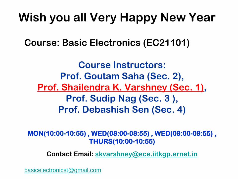
Wish you all Very Happy New Year
Course: Basic Electronics (EC21101)
Course Instructors: Prof. Goutam Saha (Sec. 2),
Prof. Shailendra K. Varshney (Sec. 1), Prof. Sudip Nag (Sec. 3 ),
Prof. Debashish Sen (Sec. 4)
Contact Email: [email protected]
MON(10:00-10:55) , WED(08:00-08:55) , WED(09:00-09:55) , THURS(10:00-10:55)
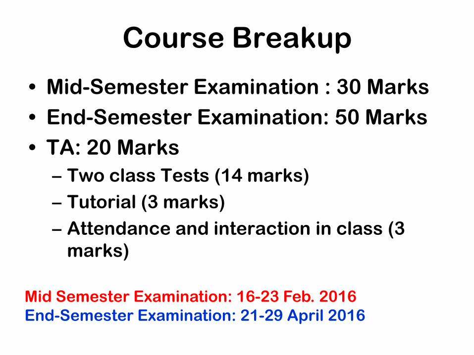
Course Breakup
• Mid-Semester Examination : 30 Marks• End-Semester Examination: 50 Marks• TA: 20 Marks
– Two class Tests (14 marks)– Tutorial (3 marks)– Attendance and interaction in class (3
marks)
Mid Semester Examination: 16-23 Feb. 2016End-Semester Examination: 21-29 April 2016
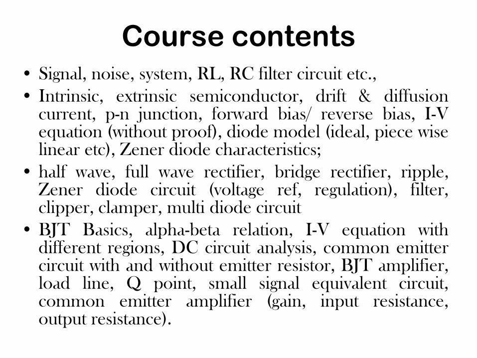
Course contents• Signal, noise, system, RL, RC filter circuit etc.,• Intrinsic, extrinsic semiconductor, drift & diffusion
current, p-n junction, forward bias/ reverse bias, I-Vequation (without proof), diode model (ideal, piece wiselinear etc), Zener diode characteristics;
• half wave, full wave rectifier, bridge rectifier, ripple,Zener diode circuit (voltage ref, regulation), filter,clipper, clamper, multi diode circuit
• BJT Basics, alpha-beta relation, I-V equation withdifferent regions, DC circuit analysis, common emittercircuit with and without emitter resistor, BJT amplifier,load line, Q point, small signal equivalent circuit,common emitter amplifier (gain, input resistance,output resistance).
Course contents
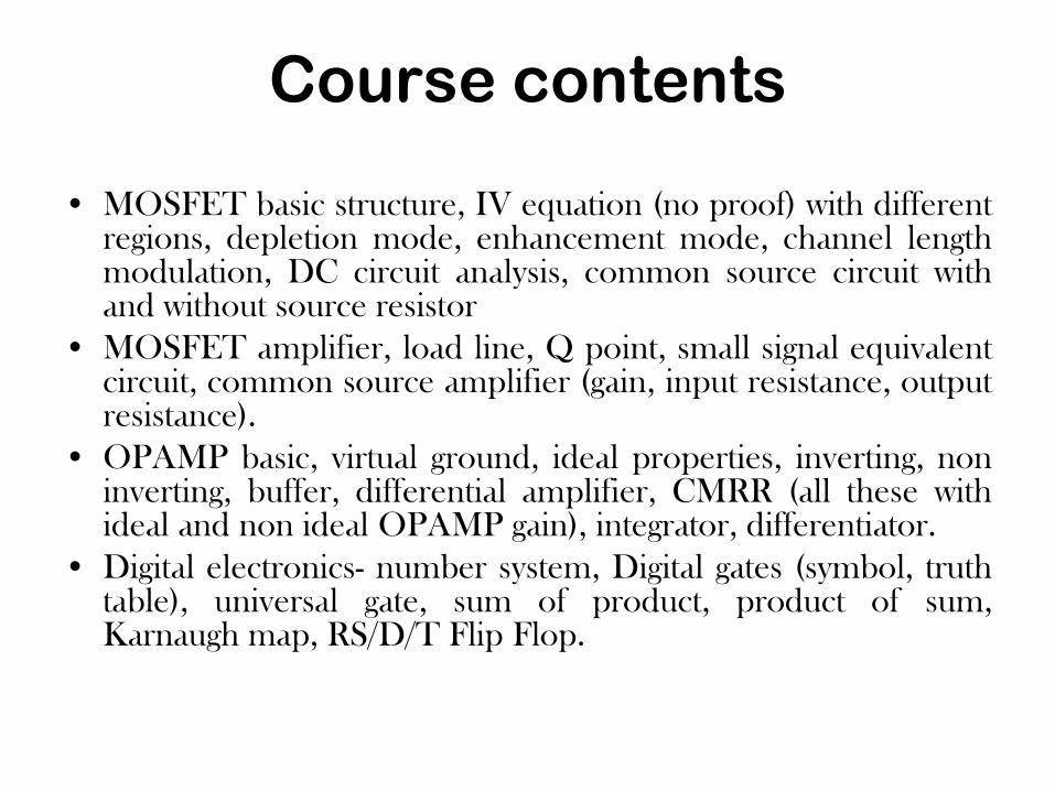
• MOSFET basic structure, IV equation (no proof) with differentregions, depletion mode, enhancement mode, channel lengthmodulation, DC circuit analysis, common source circuit withand without source resistor
• MOSFET amplifier, load line, Q point, small signal equivalentcircuit, common source amplifier (gain, input resistance, outputresistance).
• OPAMP basic, virtual ground, ideal properties, inverting, noninverting, buffer, differential amplifier, CMRR (all these withideal and non ideal OPAMP gain), integrator, differentiator.
• Digital electronics- number system, Digital gates (symbol, truthtable), universal gate, sum of product, product of sum,Karnaugh map, RS/D/T Flip Flop.
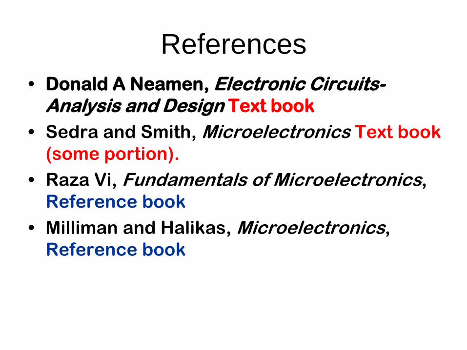
References• Donald A Neamen, Electronic Circuits-
Analysis and Design Text book• Sedra and Smith, Microelectronics Text book
(some portion).• Raza Vi, Fundamentals of Microelectronics,
Reference book• Milliman and Halikas, Microelectronics,
Reference book
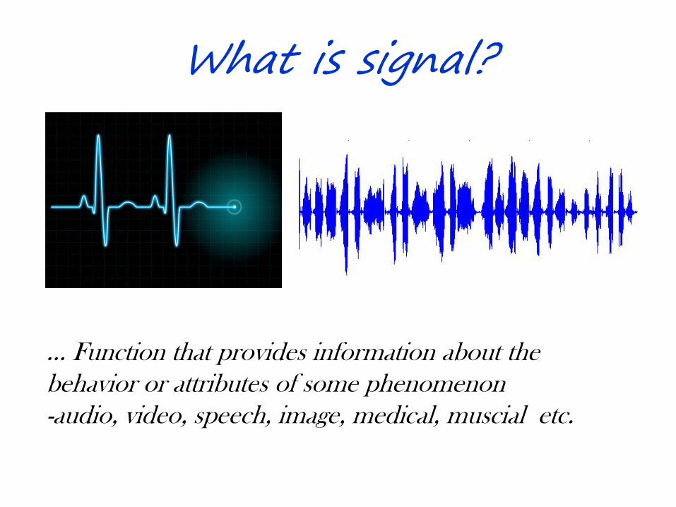
What is signal?
… Function that provides information about the behavior or attributes of some phenomenon-audio, video, speech, image, medical, muscial etc.
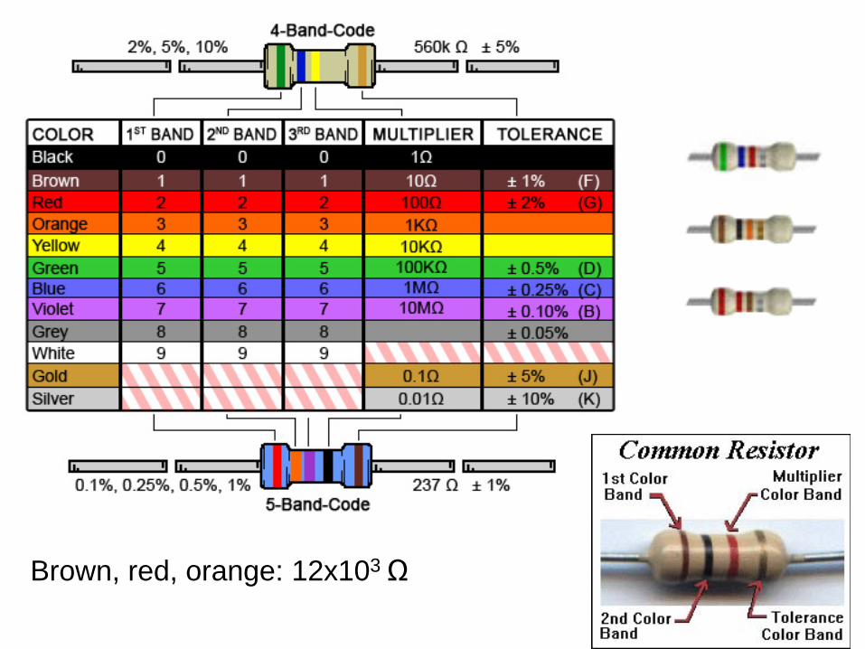
Brown, red, orange: 12x103 Ω
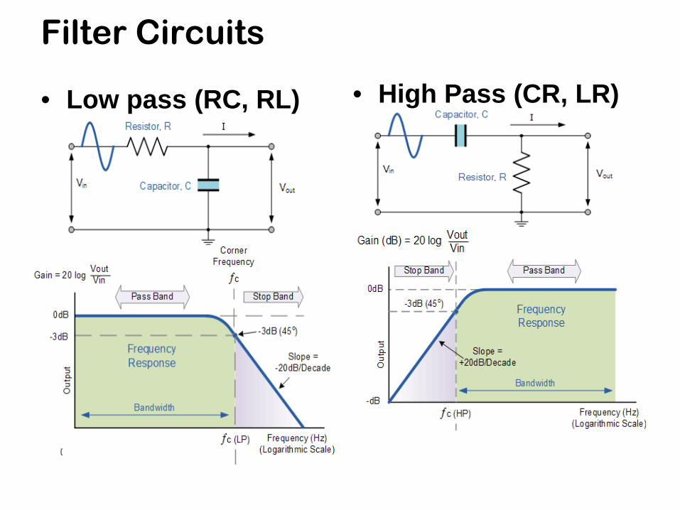
Filter Circuits
• Low pass (RC, RL) • High Pass (CR, LR)
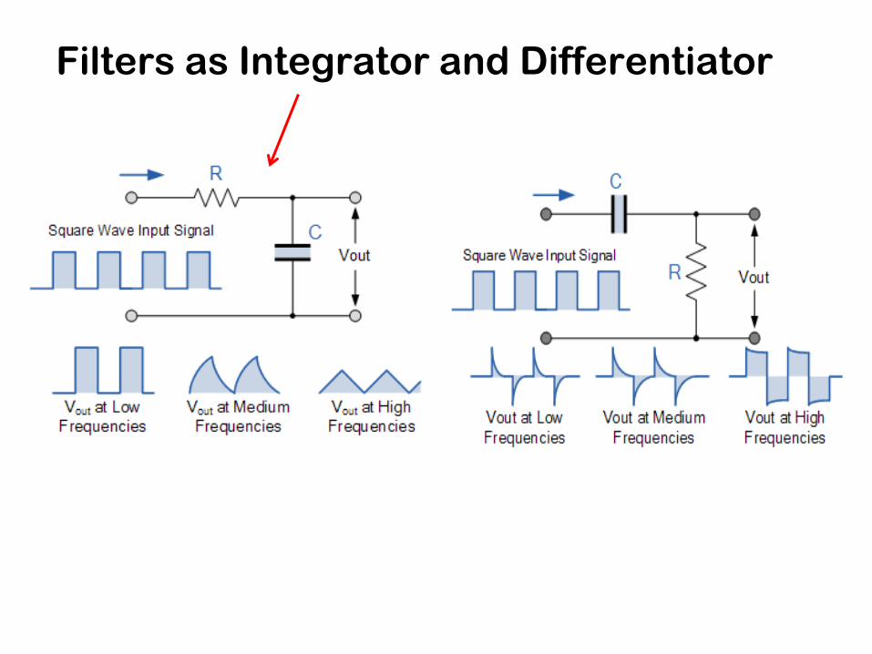
Filters as Integrator and Differentiator
Semiconductor physics
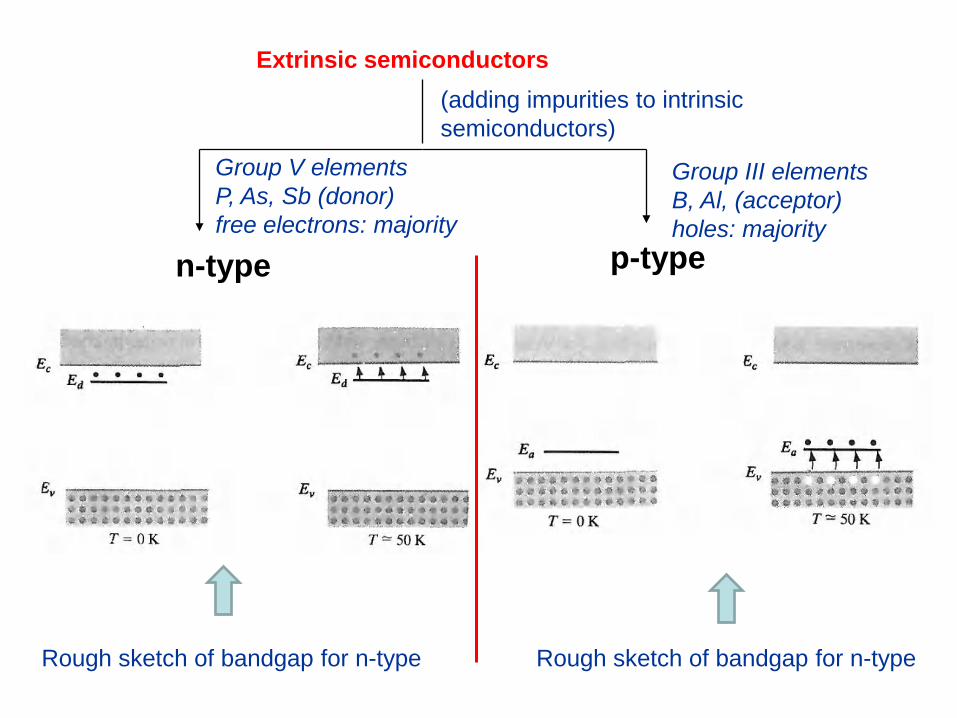
Extrinsic semiconductors
n-type p-type
(adding impurities to intrinsic semiconductors)
Group V elementsP, As, Sb (donor)free electrons: majority
Group III elementsB, Al, (acceptor)holes: majority
Rough sketch of bandgap for n-type Rough sketch of bandgap for n-type
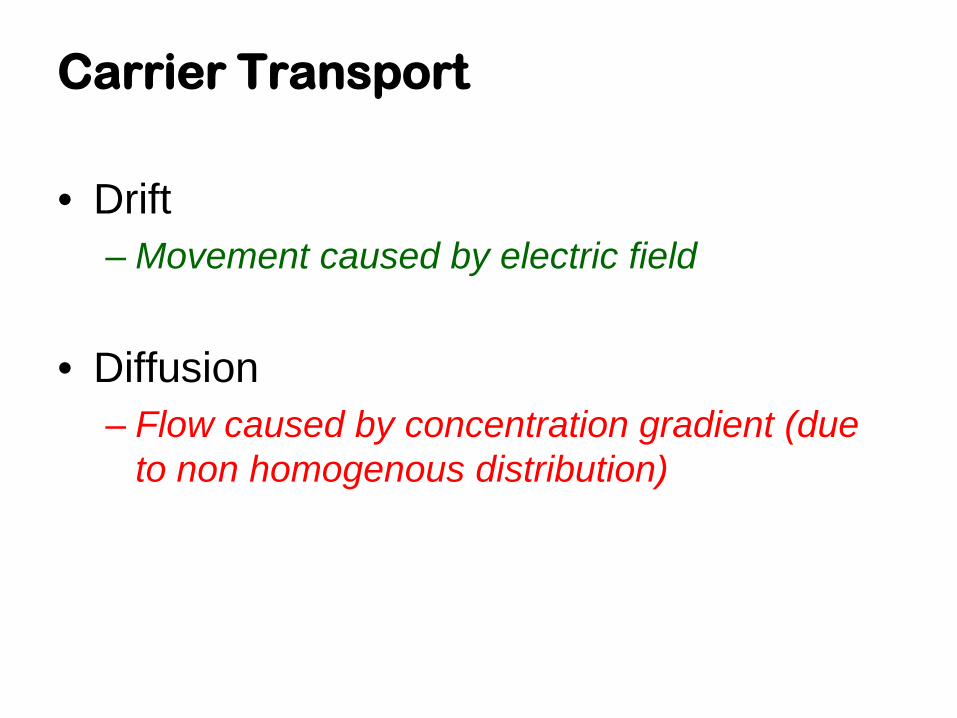
Carrier Transport
• Drift– Movement caused by electric field
• Diffusion– Flow caused by concentration gradient (due
to non homogenous distribution)
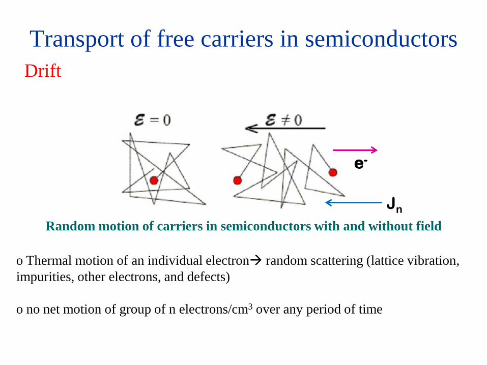
Transport of free carriers in semiconductorsDrift
Random motion of carriers in semiconductors with and without field
o Thermal motion of an individual electron random scattering (lattice vibration, impurities, other electrons, and defects)
o no net motion of group of n electrons/cm3 over any period of time
e-
Jn
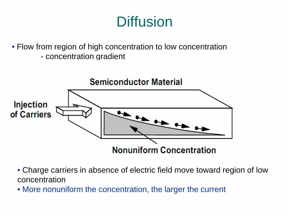
Diffusion• Flow from region of high concentration to low concentration
- concentration gradient
• Charge carriers in absence of electric field move toward region of low concentration• More nonuniform the concentration, the larger the current
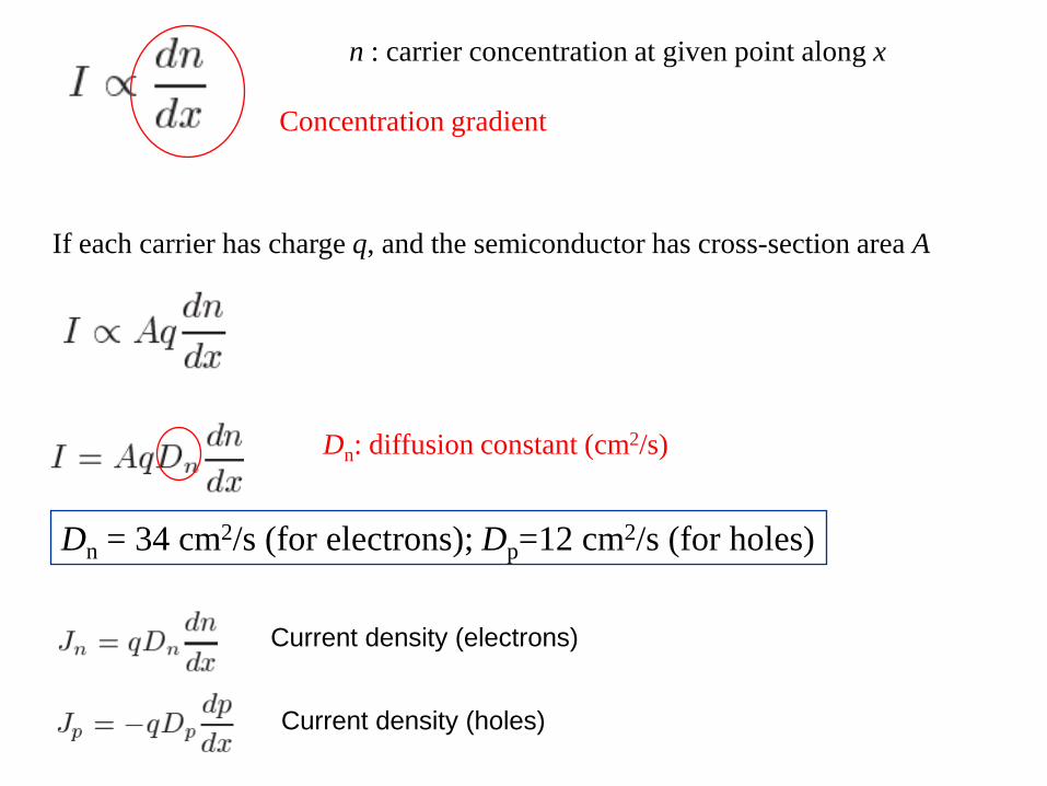
n : carrier concentration at given point along x
Concentration gradient
If each carrier has charge q, and the semiconductor has cross-section area A
Dn: diffusion constant (cm2/s)
Dn = 34 cm2/s (for electrons); Dp=12 cm2/s (for holes)
Current density (electrons)
Current density (holes)
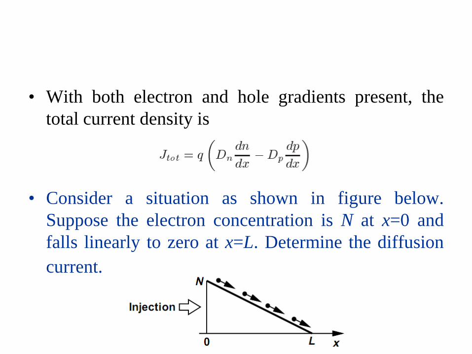
• With both electron and hole gradients present, thetotal current density is
• Consider a situation as shown in figure below.Suppose the electron concentration is N at x=0 andfalls linearly to zero at x=L. Determine the diffusioncurrent.
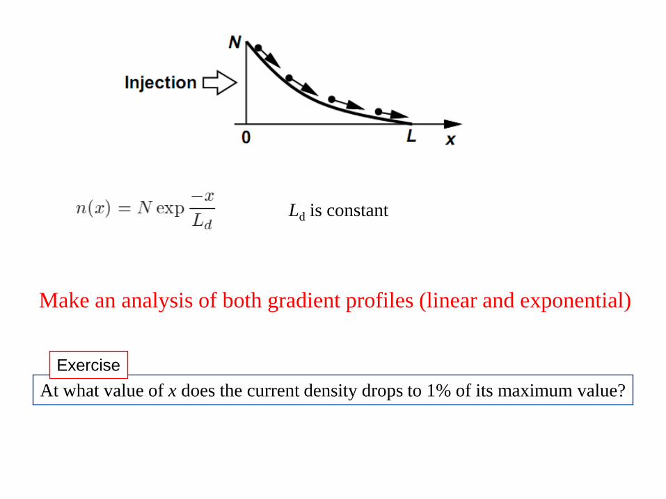
Ld is constant
Make an analysis of both gradient profiles (linear and exponential)
At what value of x does the current density drops to 1% of its maximum value?Exercise
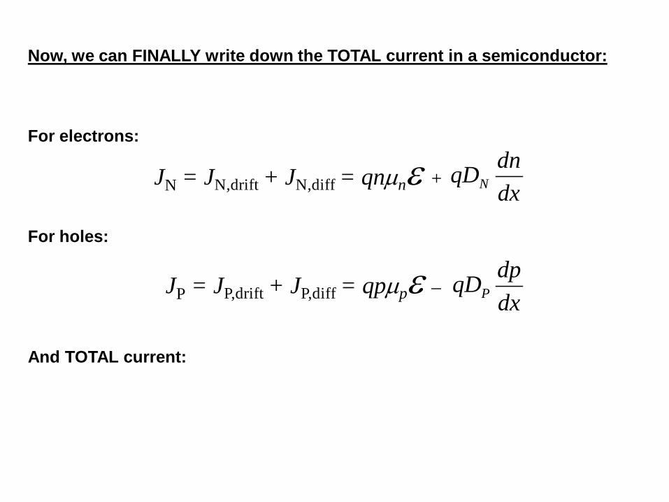
Now, we can FINALLY write down the TOTAL current in a semiconductor:
For electrons:
For holes:
And TOTAL current:
JN = JN,drift + JN,diff = qnµnε + dxdnqDN
JP = JP,drift + JP,diff = qpµpε –dxdpqDP
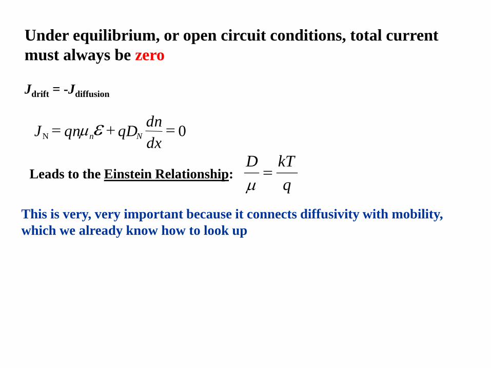
Under equilibrium, or open circuit conditions, total current must always be zero
Jdrift = -Jdiffusion
0=+=dxdnqDqnJ NnN µ ε
Leads to the Einstein Relationship:q
kTD=
µ
This is very, very important because it connects diffusivity with mobility, which we already know how to look up
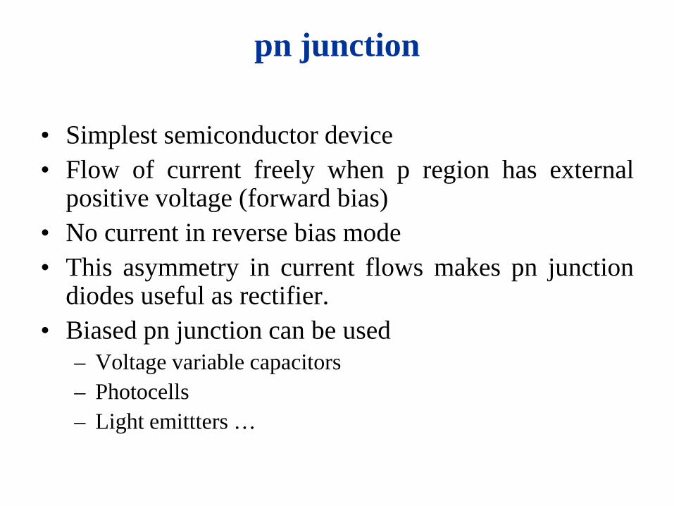
pn junction
• Simplest semiconductor device• Flow of current freely when p region has external
positive voltage (forward bias)• No current in reverse bias mode• This asymmetry in current flows makes pn junction
diodes useful as rectifier.• Biased pn junction can be used
– Voltage variable capacitors– Photocells– Light emittters …
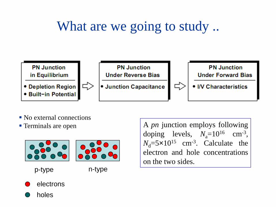
What are we going to study ..
No external connections Terminals are open
p-type n-type
electronsholes
A pn junction employs followingdoping levels, Na=1016 cm-3,Nd=5×1015 cm-3. Calculate theelectron and hole concentrationson the two sides.
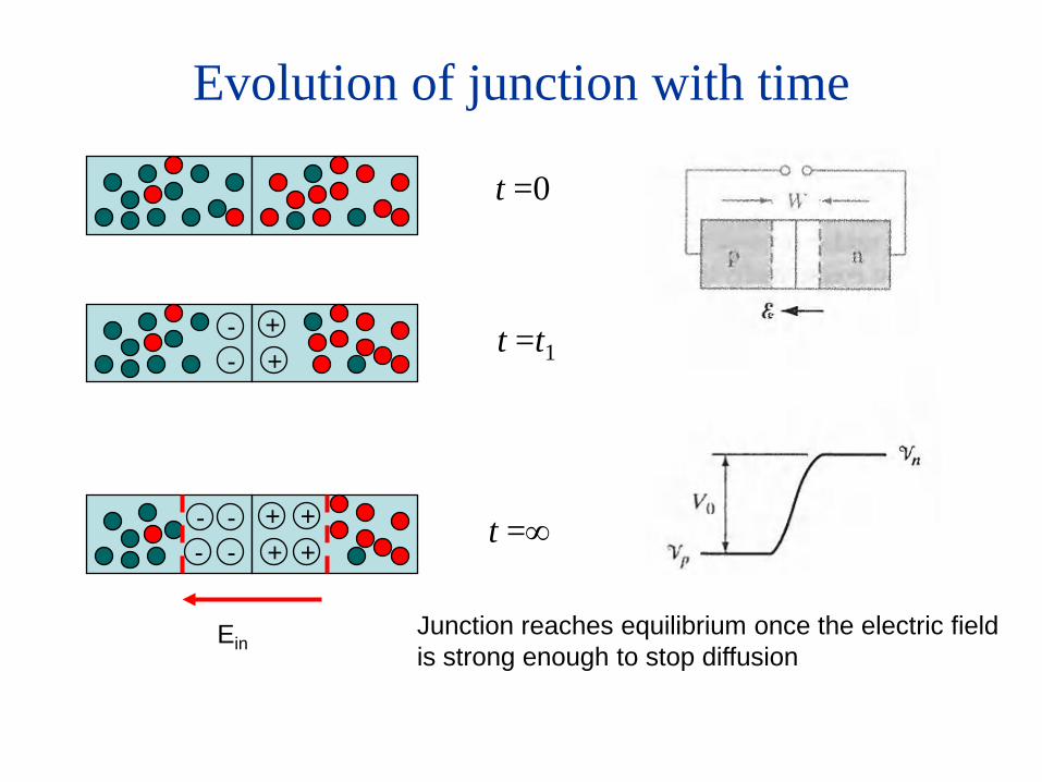
t =0
++
--
Evolution of junction with time
t =t1
t =∞++
---
-++
EinJunction reaches equilibrium once the electric field is strong enough to stop diffusion
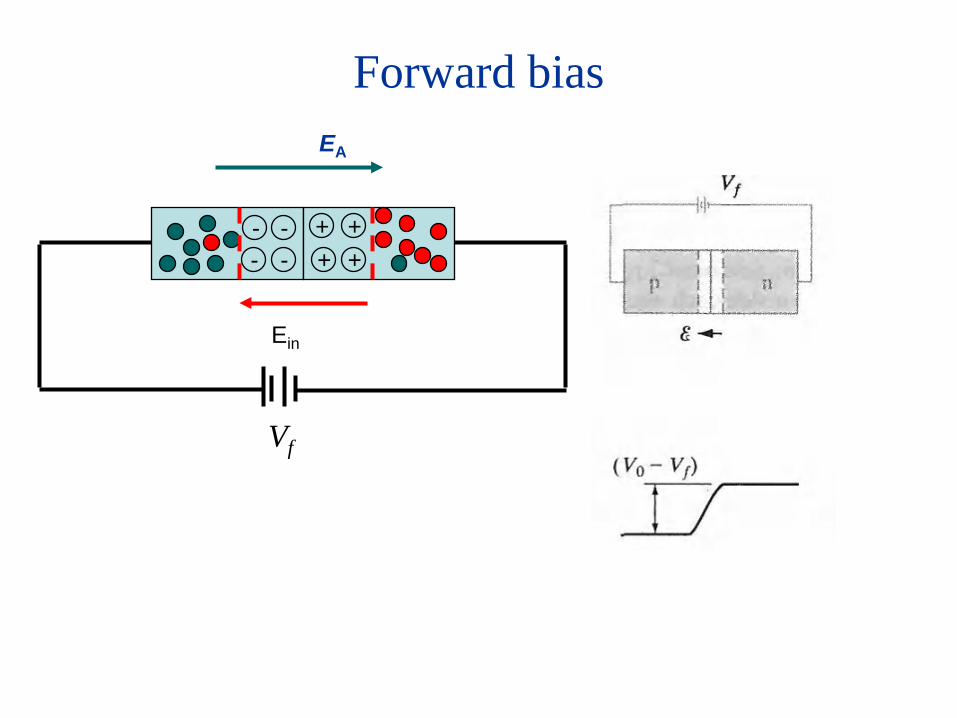
Forward bias
++
---
-++
Ein
Vf
EA
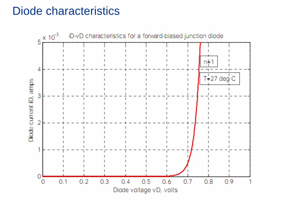
Diode characteristics
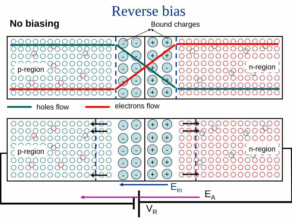
Reverse bias
- -
- -
- -
- -
- -
+ +
+ +
+ -
+ +
+ +
No biasing
p-region n-region
holes flow electrons flow
Bound charges
- -
- -
- -
- -
- -
+ +
+ +
+ -
+ +
+ +
p-region n-region
VR
Ein EA
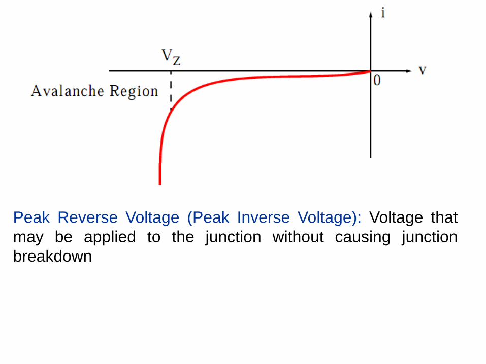
Peak Reverse Voltage (Peak Inverse Voltage): Voltage thatmay be applied to the junction without causing junctionbreakdown
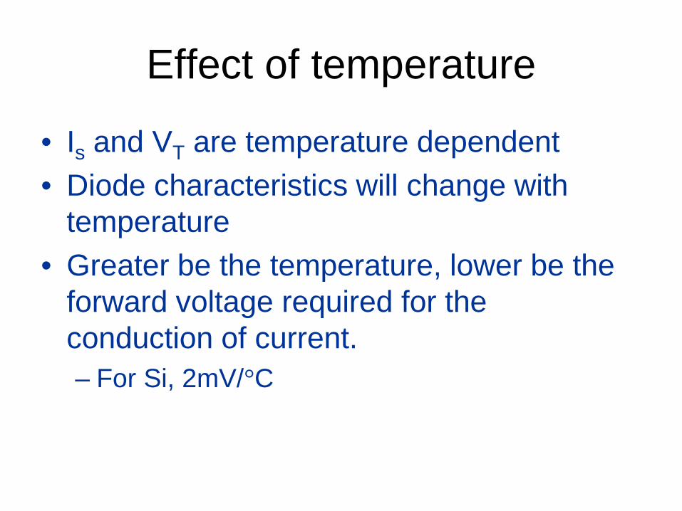
Effect of temperature
• Is and VT are temperature dependent• Diode characteristics will change with
temperature• Greater be the temperature, lower be the
forward voltage required for the conduction of current.– For Si, 2mV/°C
Breakdown in Diodes
• Zener breakdown• Avalance breakdown
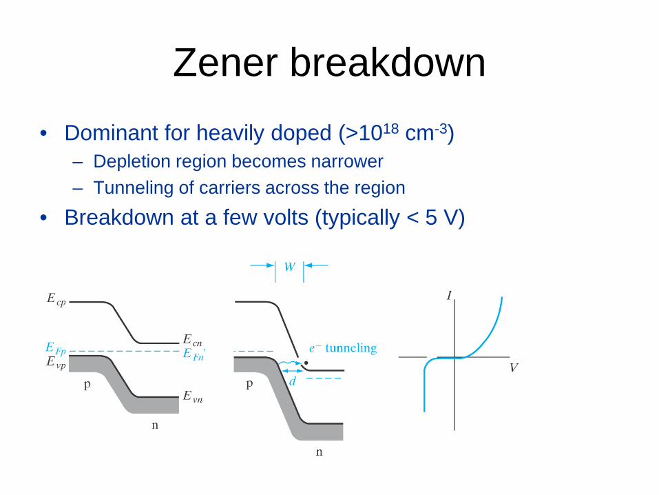
Zener breakdown• Dominant for heavily doped (>1018 cm-3)
– Depletion region becomes narrower– Tunneling of carriers across the region
• Breakdown at a few volts (typically < 5 V)
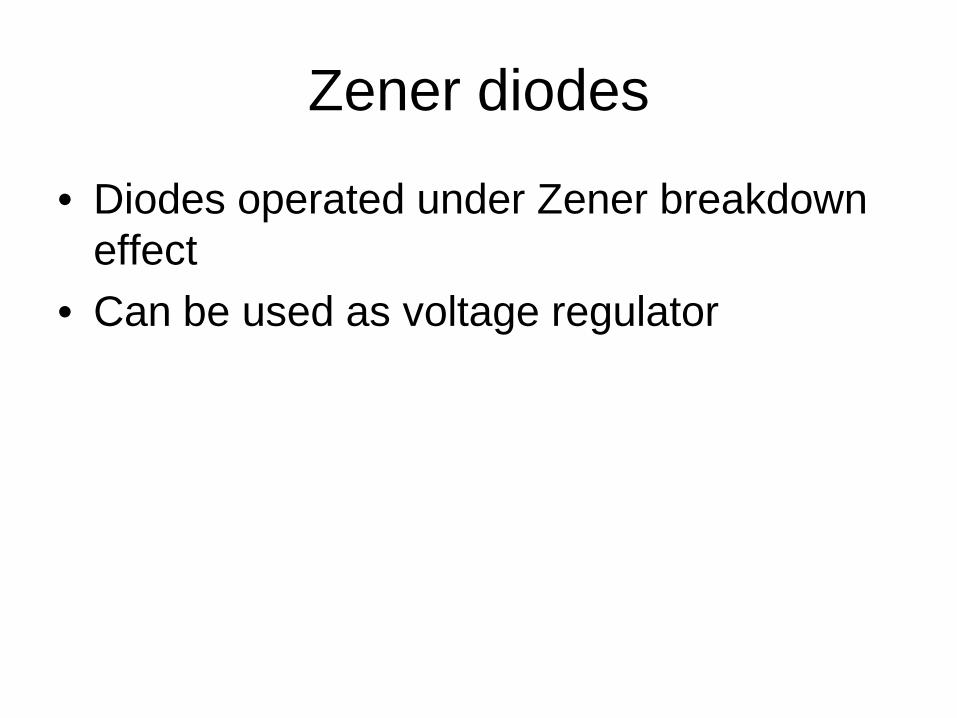
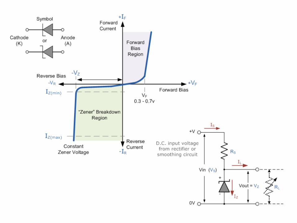
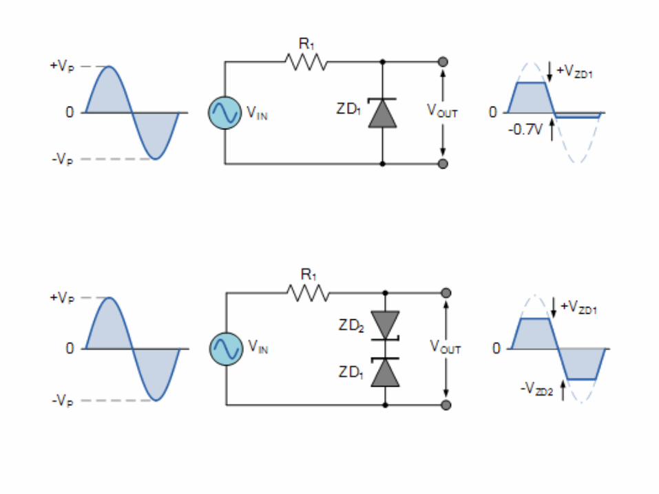
Zener diodes
• Diodes operated under Zener breakdown effect
• Can be used as voltage regulator
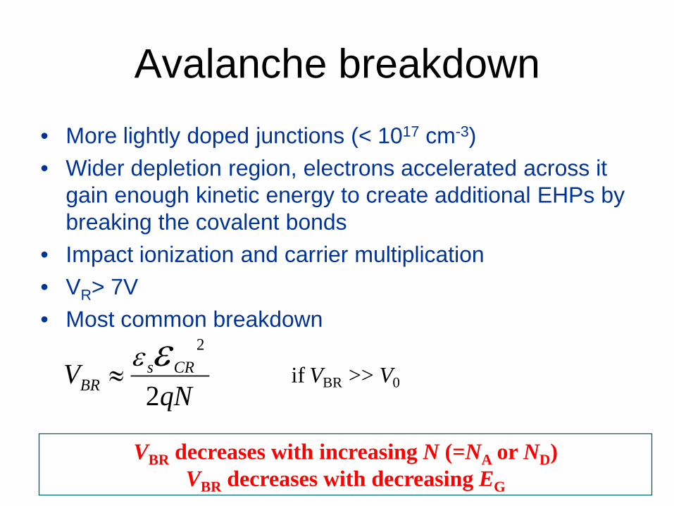
Avalanche breakdown• More lightly doped junctions (< 1017 cm-3)• Wider depletion region, electrons accelerated across it
gain enough kinetic energy to create additional EHPs by breaking the covalent bonds
• Impact ionization and carrier multiplication• VR> 7V• Most common breakdown
qNV CRs
BR 2
2εε≈ if VBR >> V0
VBR decreases with increasing N (=NA or ND)VBR decreases with decreasing EG
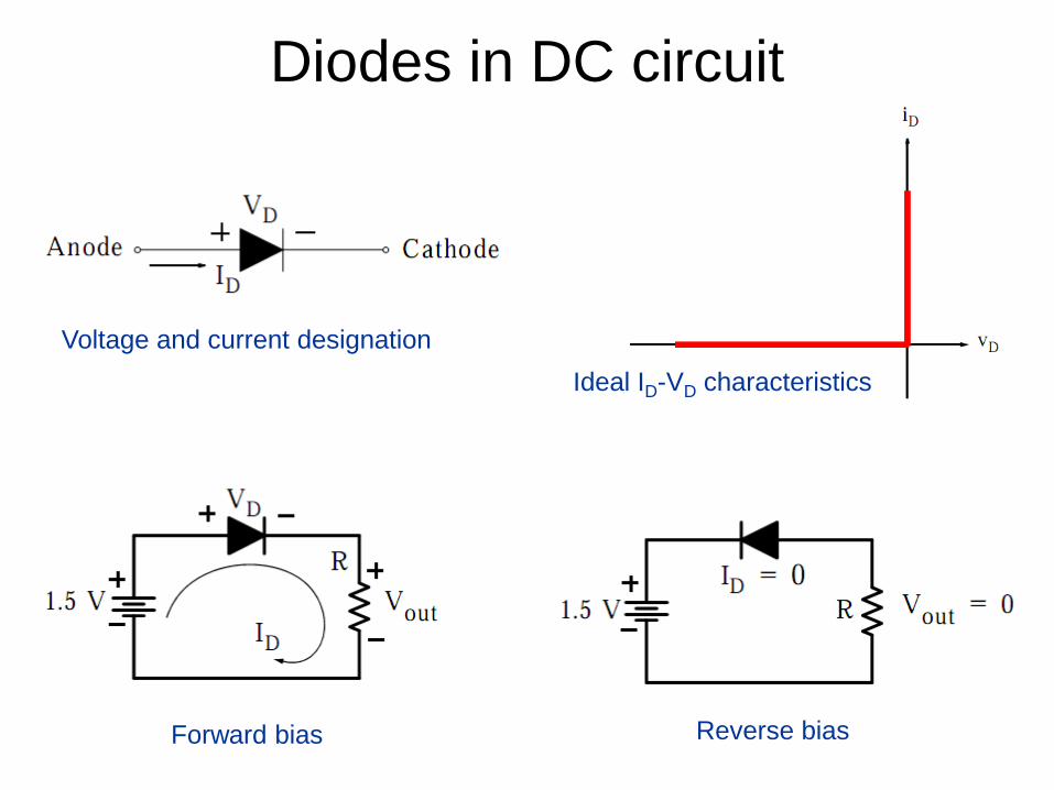
Diodes in DC circuit
Forward bias Reverse bias
Voltage and current designation Ideal ID-VD characteristics
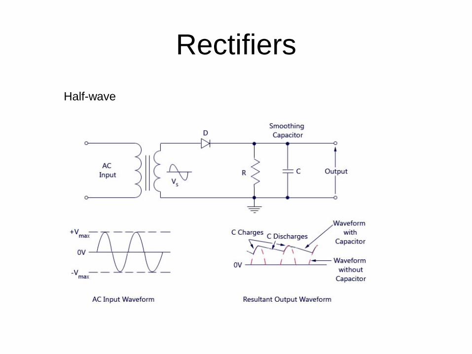
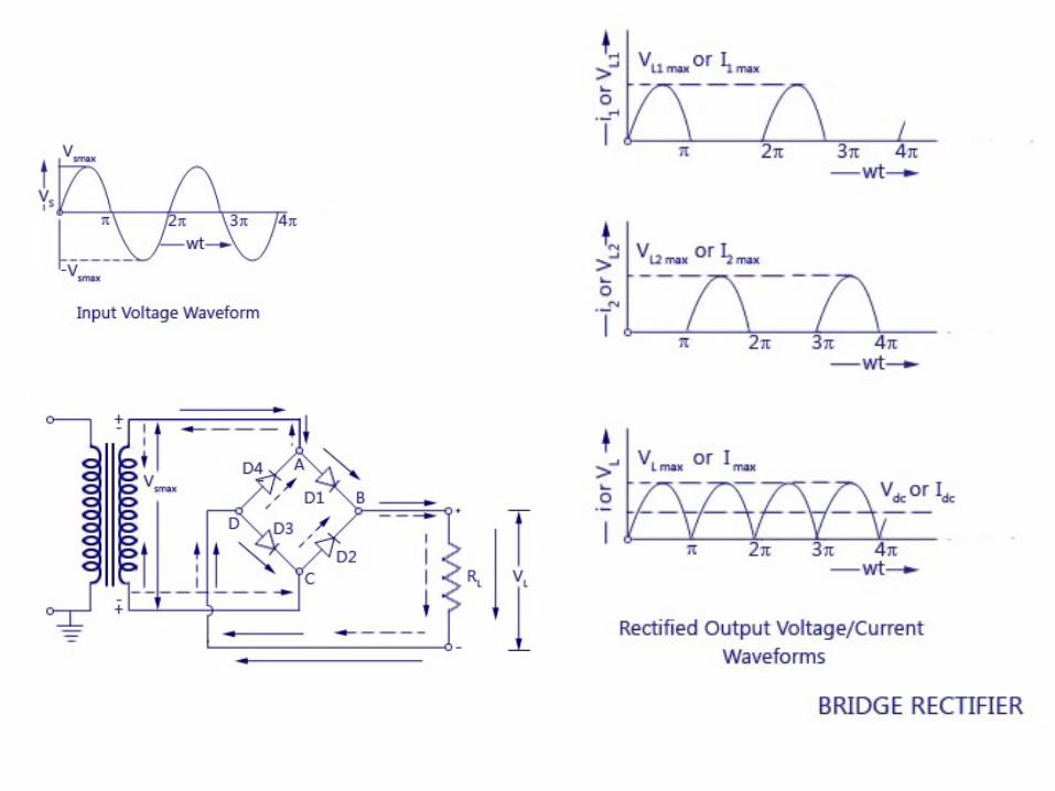
RectifiersHalf-wave
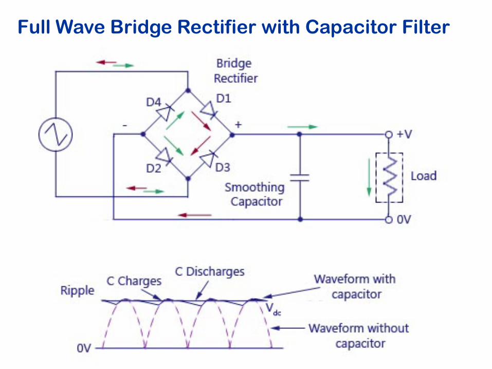
Full Wave Bridge Rectifier with Capacitor Filter
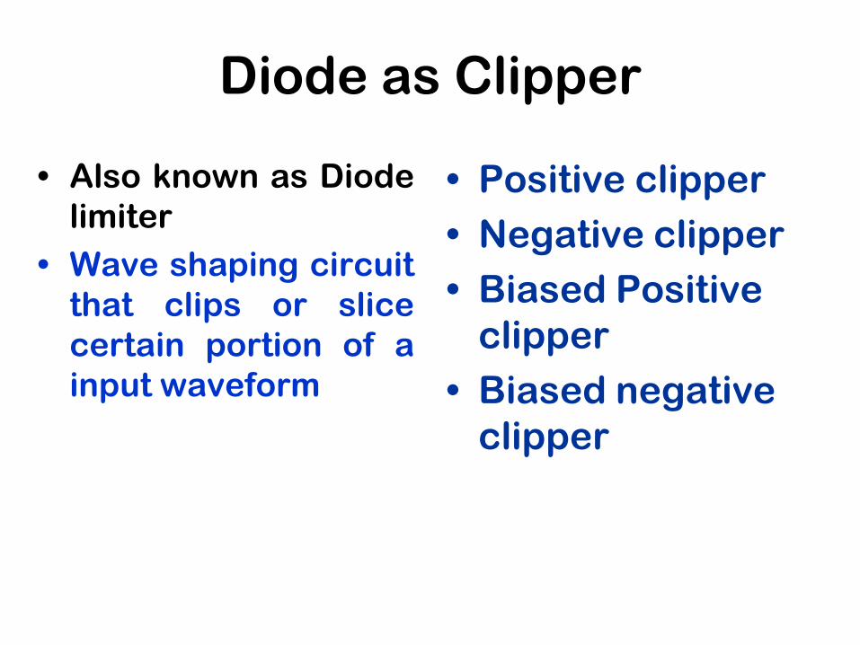
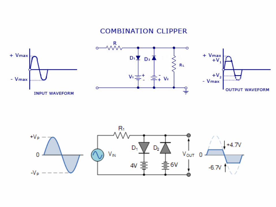
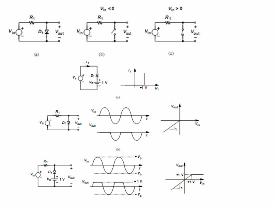
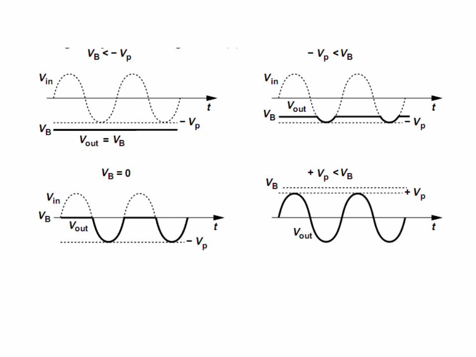
Diode as Clipper
• Also known as Diodelimiter
• Wave shaping circuitthat clips or slicecertain portion of ainput waveform
• Positive clipper• Negative clipper• Biased Positive
clipper• Biased negative
clipper
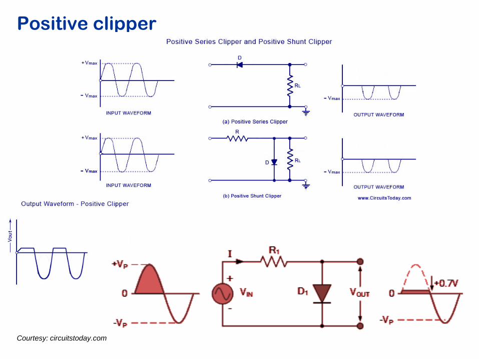
Positive clipper
Courtesy: circuitstoday.com
Courtesy: circuitstoday.com
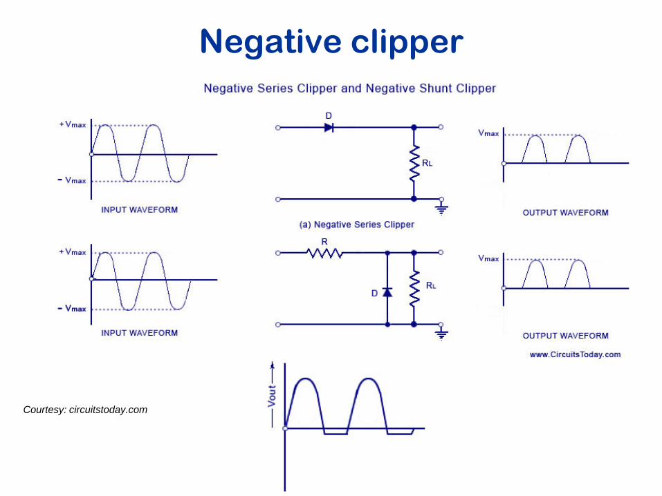
Negative clipper
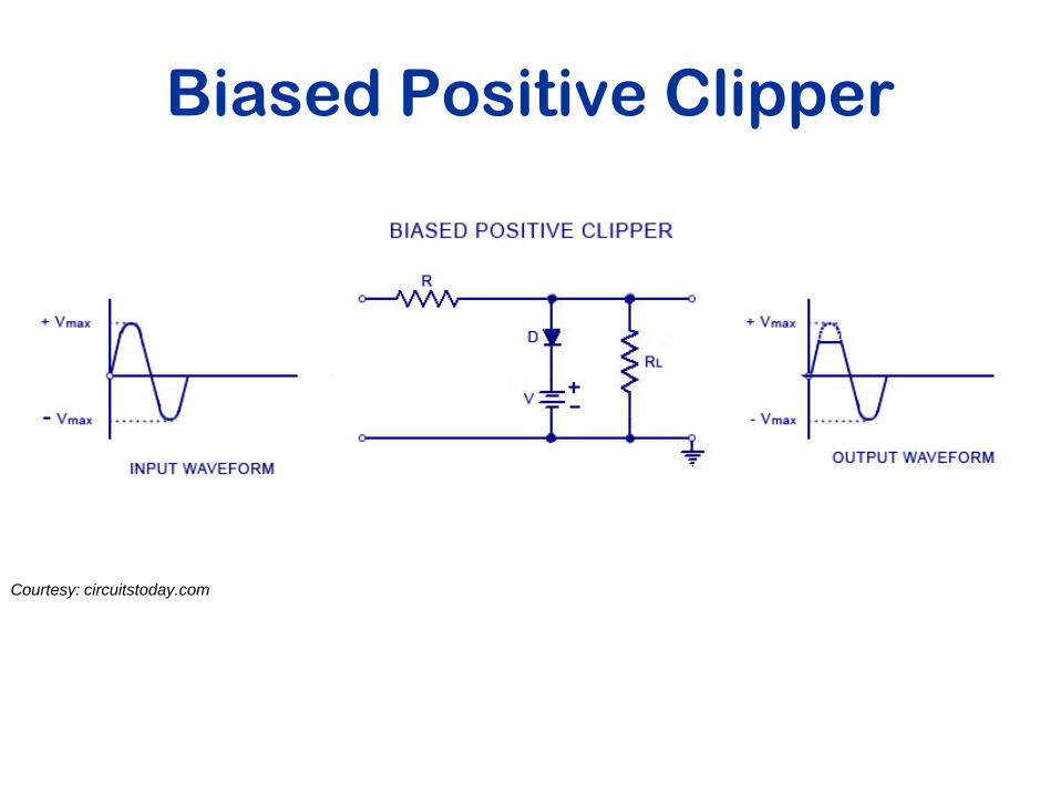
Biased Positive Clipper
Courtesy: circuitstoday.com
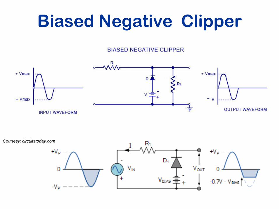
Biased Negative Clipper
Courtesy: circuitstoday.com
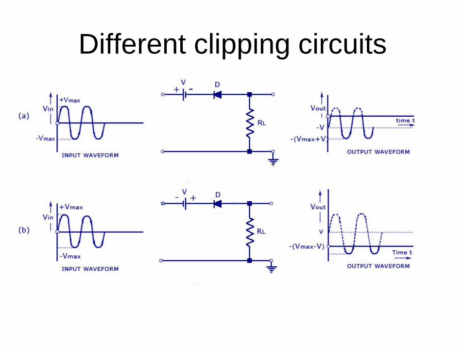
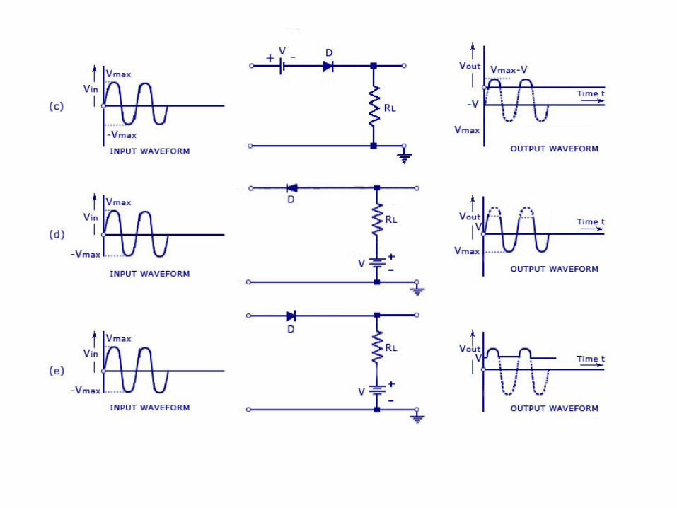
Different clipping circuits
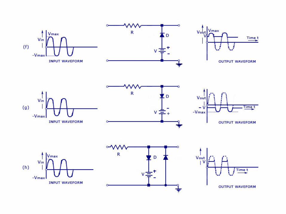
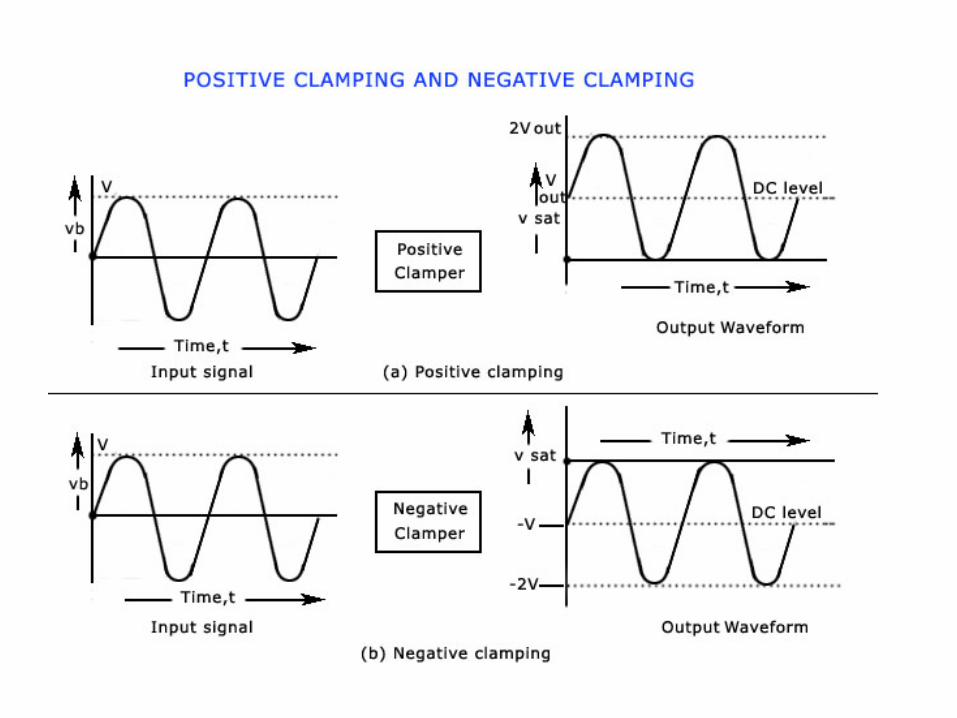
Diode as Clamper
• A clamping circuit isused to place either thepositive or negativepeak of a signal at adesired level.
• The dc component issimply added orsubtracted to/from theinput signal. Theclamper is alsoreferred to as an ICrestorer and ac signallevel shifter.