Embed Size (px)
Citation preview

Chapter 6
Practical Implementation
Issues
6.1 INTRODUCTION
The design of a wireless sensor network is more than the design of a com-munication protocol. The design of the actual network nodes is critical tothe success of the network (i.e., to how well the network meets the needsof the application). Several features of the design of wireless sensor net-work nodes are unique (or nearly so) to the design of small, battery-pow-ered wireless devices, and are not often encountered in the design of othertypes of electronic equipment. For example, in the design of a cellular tele-phone or other land mobile communications system, the primary cost tobe borne in mind during development is the cost of the system infrastruc-ture — the base stations, towers, switching equipment, etc. — both as aninitial capital outlay and then as monthly rental, depreciation, and mainte-nance expense. To make the system economically viable, this equipmentmust service the largest possible number of users to defray these fixedcosts among them to the point that the service is affordable. The cost ofthe individual mobile handset is, to a very large degree, irrelevant whencompared with the infrastructure cost; not only is its cost relatively lowwhen compared with the infrastructure cost, its maintenance cost is alsonegligible — and often borne by the user, in any event, in the form of elec-tricity to recharge the battery.
Because the system design has a goal to maximize the number of userssupported by the infrastructure equipment, sophisticated techniques (ofmodulation, coding, etc.) are employed to do this, even if the cost of thehandset is raised significantly — because the total cost to the user, whenthe system infrastructure costs are factored in, will be lower.
The situation with wireless sensor networks is quite different. Becauseno infrastructure is associated with the ad hoc networks they employ, theeconomics of wireless sensor networks only consider the cost of the indi-vidual network node. This greatly changes the design goal from that of the
AU1823_C06.fm Page 115 Monday, July 14, 2003 7:03 AM
©2004 CRC Press LLC
land mobile system designer. Instead of designing for the maximum possi-ble system capacity, the designer must design for the lowest possible unitcost (consistent with the other network goals, of course). This places thedesign emphasis squarely on the product cost of the network nodebecause its cost of operation (electricity, etc.) is trivial and focuses thedesigner’s attention on some network node features that typically receivelittle attention in other services.
This chapter discusses a few of these more unique features, includingsome subtleties involved in deciding how much of the network nodeshould be integrated (and into which chips), the importance of sensorinterfaces, and the interrelationship between time base accuracy and thepower consumption of the network node.
6.2 THE PARTITIONING DECISION
The conversion of a system block diagram into an end user product is acomplex one, with trade-offs evaluated and decisions made at several lev-els in the design process. The decisions are especially critical in the designof a wireless sensor network node, due to the enormous attention paid toproduct cost. A too-conservative integration strategy can price a manufac-turer out of the market, while a too-aggressive strategy may result in insur-mountable technical difficulties, or (perhaps worse) a functioning product,but one useful only in a market too small to produce a useful return on theengineering investment. Although some flexibility may be retained by pro-grammability, it nevertheless remains true that integration is a form ofproduct specialization, and, just as in biology, there is an optimum amountof specialization for a given velocity of environmental change.
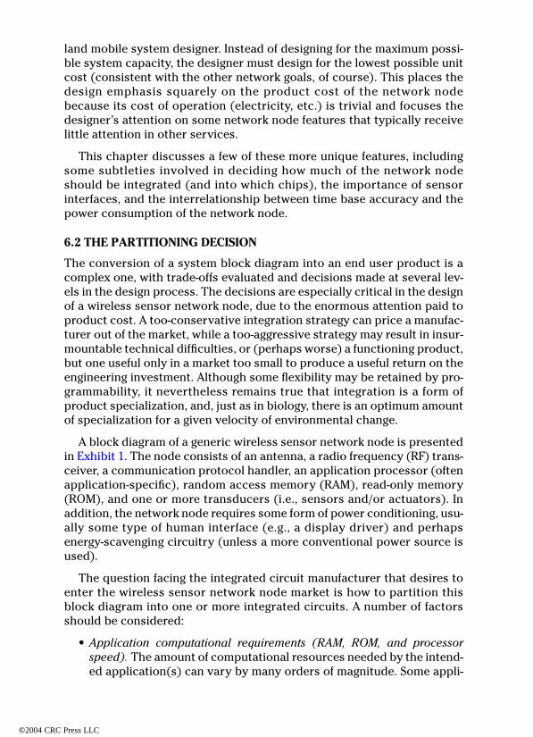
A block diagram of a generic wireless sensor network node is presentedin Exhibit 1. The node consists of an antenna, a radio frequency (RF) trans-ceiver, a communication protocol handler, an application processor (oftenapplication-specific), random access memory (RAM), read-only memory(ROM), and one or more transducers (i.e., sensors and/or actuators). Inaddition, the network node requires some form of power conditioning, usu-ally some type of human interface (e.g., a display driver) and perhapsenergy-scavenging circuitry (unless a more conventional power source isused).
The question facing the integrated circuit manufacturer that desires toenter the wireless sensor network node market is how to partition thisblock diagram into one or more integrated circuits. A number of factorsshould be considered:
•
Application computational requirements (RAM, ROM, and processorspeed).
The amount of computational resources needed by the intend-ed application(s) can vary by many orders of magnitude. Some appli-
AU1823_C06.fm Page 116 Monday, July 14, 2003 7:03 AM
©2004 CRC Press LLC
cations may require almost none at all; inputs to and from thetransducer are simply passed directly to the protocol handler as datawith just a slight amount of formatting required. Other applicationsmay require extensive computational resources — for instance, if theoperation of the transducer is complex or if significant post-process-ing of the data (e.g., a fast Fourier transform) is required. Additionalresources are required if the wireless sensor network is required toperform data fusion — the analysis and condensation of data receivedfrom other network nodes — in addition to processing its own data. Fi-nally, although the processing required of each transducer may besimple, a single network node may support a large number of trans-ducers. The device manufacturer must then choose between a rela-tively inexpensive design of limited capability, incorporating only asmall amount of RAM and ROM, or a more capable but more expensivedesign incorporating more RAM and ROM and a faster processor.
•
Ability to use host resources.
Often a wireless sensor network node isincorporated in other, larger systems, such as a personal digital assis-tant (PDA), cellular telephone, or even a fixed asset such as a buildingenvironmental controller. In these applications, resources (especiallycomputational resources) may be available from the host. Havingsuch resources available means that they do not have to be suppliedby the wireless sensor node itself; the designer may take advantage ofthis fact, remove duplicate resources from the network node design,and reduce its cost accordingly. The penalty, of course, is that the total
Exhibit 1. A Generic Wireless Sensor Network Node
AU1823_C06.fm Page 117 Monday, July 14, 2003 7:03 AM
©2004 CRC Press LLC
available market for this product has now shrunk to that with support-ing hosts.
•
Desired market flexibility.
The integration of specific energy scaveng-ing and power conditioning circuits reduces cost and improves effi-ciency, but limits the design to a particular power source. Separatingthe power source and conditioning circuits from the rest of the net-work node design enables a single design to be reused with multipleexternal sources and conditioning circuits, albeit at higher marginalproduct cost and lower overall efficiency. Integration of a particulartransceiver requires a new chip if use in a new band, or a new protocolin an existing band, is envisioned. For example, the manufacturer of afully integrated 900-MHz product line that wishes to expand its prod-uct line to include a 2450-MHz product must duplicate its entire line. Ifthe transceiver is not integrated with the rest of the network node, theexisting chips in the product line may remain, and only an interface-compatible 2450-MHz transceiver need be designed — a much easiertask. Having market flexibility is especially important in emerging, im-mature markets, such as those for wireless sensor networks, in whichthe largest volume niches may not be proven and standard designsnot yet adopted.
•
Product physical size goals.
Of course, a direct trade-off exists betweenthe level of system integration and final product physical size; howev-er, certain applications do not require the absolute minimum physicalsize of the network node circuits. For example, total system integra-tion will often result in a design that is smaller than its user interface.It is relatively pointless to reduce the network node circuit area to 1cm
2
if, for instance, a keypad and display are required for a user to en-ter a security code — especially if increasing integration is increasing-ly expensive due to the need for an expensive, specialized integratedcircuit (IC) process. Similar arguments can be made concerning therelative sizes of batteries and antennas.
•
Required time to market.
A critical point in the electronics industry istime to market. A fully integrated wireless sensor network node is acomplex, mixed-signal (i.e., containing both analog and digital cir-cuits) design that takes time to design, test, and debug. However, itscomponents — processors, transceivers, etc. — are either availableoff-the-shelf or are much simpler to design as stand-alone chips.Therefore, one desiring to enter the market and receive revenue quick-ly may choose a less integrated design to start, perhaps while workingon a more integrated design to follow as the market matures.
•
Network heterogeneity.
Many wireless sensor networks support multi-ple types of network nodes, having different capabilities. For example,the Institute of Electrical and Electronics Engineers (IEEE) 802.15.4standard
1
specifies two types of devices: a Full Function Device (FFD)
AU1823_C06.fm Page 118 Monday, July 14, 2003 7:03 AM
©2004 CRC Press LLC
and a Reduced Function Device (RFD). The FFD may be the master(called the “PAN Coordinator” in the IEEE 802.15.4 standard) of a starnetwork and, therefore, must have enough memory to store addressinformation of all devices in the network. In a star network, an RFDmay be only a slave, and thus needs memory only sufficient to storethe address of the network master. Most manufacturers would want tosell both types; to enable both FFD and RFD functionality, they mayelect to design one chip with programming to support either of thesefunctions. Because the RFD design then has the memory required forthe FFD, however, its cost of production is not as low as an RFD-onlydesign. To enable a low-cost RFD design, the manufacturer may electto design a second fully integrated RFD chip; however, an alternativecan be to design only one chip for both FFD and RFD, but not includingthe processing function. Instead, the chip can have an interface to anexternal microcontroller. This approach, although not having many ofthe benefits of full integration (small size, low cost, etc.) does have theadvantage of flexibility; the external microcontroller can be matchedto the processing needs at hand — whether for RFD, FFD, or even tosupport specific applications.
•
Digital logic.
To minimize costs, digital logic should be placed in the ICprocess with the highest possible complementary metal oxide semi-conductor (CMOS) gate density. This process usually supports onlyCMOS logic, i.e., without additional features such as bipolar devices(BiCMOS), high-quality integrated analog passive components, ormemory cells.
•
RF and analog performance.
IC processes optimized for RF and analogperformance usually include bipolar transistors, high-quality inductorsand capacitors, and large value resistors. Recent lithographic improve-ments in CMOS processes have made metal oxide semiconductor(MOS) devices useful at RF; however, their noise and device-matchingbehavior (two process features important for most RF and analog de-sign) are still inferior to that of bipolar devices.
•
Need for high-voltage operation.
State-of-the-art CMOS processes havelimited voltage capability; even a dual-oxide process often cannot sup-port devices switching more than 3.6 V or so. Many circuits, particu-larly energy scavenging, power conversion, and user interfacecircuits, may need to support higher voltages.
•
Need for high-current operation.
Some transducers may need signifi-cant amounts of current to operate. In addition, some actuators mayneed to switch high currents. A specialized IC process and specializedpackaging may be necessary to support these requirements.
•
Packaging and chip-to-chip interconnect.
Packaging and chip-to-chip in-terconnect is expensive. The fewer packages that must be used, thelower the material cost and the higher the overall yield of the factory
AU1823_C06.fm Page 119 Monday, July 14, 2003 7:03 AM
©2004 CRC Press LLC
process. Chip-to-chip interconnect requires at least two interconnec-tion pads (one on each chip); such pads, whether conventional wirebond pads or pads for any of the direct chip attach (DCA) schemes,take up prodigious amounts of die area — especially when their elec-trostatic discharge (ESD) protection circuitry is included.
•
High-speed signals.
High-speed signals off-chip can consume a lot ofpower. Due to the greater capacitance of off-chip interconnect, whencompared with integrated interconnect, designs using high-speed, off-chip signals can suffer a power consumption penalty.
With this many factors to consider, no one optimum design is recom-mended. Different markets and manufacturers weigh these factors differ-ently, and so the definition of optimum varies by market and the goals ofthe manufacturer. One may evaluate several partitionings of the blockdiagram in light of these factors, however.
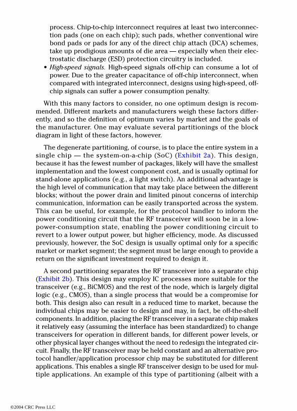
The degenerate partitioning, of course, is to place the entire system in asingle chip — the system-on-a-chip (SoC) (Exhibit 2a). This design,because it has the fewest number of packages, likely will have the smallestimplementation and the lowest component cost, and is usually optimal forstand-alone applications (e.g., a light switch). An additional advantage isthe high level of communication that may take place between the differentblocks; without the power drain and limited pinout concerns of interchipcommunication, information can be easily transported across the system.This can be useful, for example, for the protocol handler to inform thepower conditioning circuit that the RF transceiver will soon be in a low-power-consumption state, enabling the power conditioning circuit torevert to a lower output power, but higher efficiency, mode. As discussedpreviously, however, the SoC design is usually optimal only for a specificmarket or market segment; the segment must be large enough to provide areturn on the significant investment required to design it.
A second partitioning separates the RF transceiver into a separate chip(Exhibit 2b). This design may employ IC processes more suitable for thetransceiver (e.g., BiCMOS) and the rest of the node, which is largely digitallogic (e.g., CMOS), than a single process that would be a compromise forboth. This design also can result in a reduced time to market, because theindividual chips may be easier to design and may, in fact, be off-the-shelfcomponents. In addition, placing the RF transceiver in a separate chip makesit relatively easy (assuming the interface has been standardized) to changetransceivers for operation in different bands, for different power levels, orother physical layer changes without the need to redesign the integrated cir-cuit. Finally, the RF transceiver may be held constant and an alternative pro-tocol handler/application processor chip may be substituted for differentapplications. This enables a single RF transceiver design to be used for mul-tiple applications. An example of this type of partitioning (albeit with a
AU1823_C06.fm Page 120 Monday, July 14, 2003 7:03 AM
©2004 CRC Press LLC
CMOS RF transceiver) is the MC 13192 transceiver/microcomputer combina-tion described in Appendix C.
A third alternative is to move the chip partition between the protocolhandler and the application processor (Exhibit 2c). A multichip design
Exhibit 2. Some Possible Network Node Partitions
AU1823_C06.fm Page 121 Monday, July 14, 2003 7:03 AM
©2004 CRC Press LLC

based on this partition decouples the communication protocol and theapplication; a single application can operate on multiple protocols merelyby replacing the communication chip. Conversely, a manufacturer candesign a single communication chip, but optimize its solution for multipleapplications by offering several application processors, each with varyingamounts of memory and processing speed. A disadvantage of thisapproach is that the user must pay for two sets of memory: one for thecommunication chip and one for the application processor (unless anexternal memory arbitrator is employed, an expensive alternative); a sin-gle-chip approach using shared memory will usually be able to employ lesstotal memory. Memory is often a very significant fraction of componentcost in wireless sensor network nodes, therefore, the total amount of mem-ory a user must purchase is often an important factor to consider.
The previous partitionings did not explicitly place the power condition-ing circuits. An alternative partitioning is to separate the power condition-ing circuits from the rest of the node chips, as shown in Exhibit 2d for theerstwhile SoC design. This approach has several advantages:
1. The power supply specifications of the rest of the chipset can begreatly simplified; they will receive an external supply with a stan-dardized voltage provided by the power IC. This simplifies their de-sign.
2. A single chipset can be supplied by the mains, multiple types of bat-teries, or various energy scavenging techniques merely by using theappropriate power-conditioning (and maybe scavenging) chip. Thiscan open many markets without redesign of a large SoC.
3. The power-conditioning chip may be placed in an IC process bestsuited for its performance requirements, which may include rela-tively high voltages and the use of bipolar transistors and high qual-ity passive components.
A disadvantage of this approach, however, is the communication bottle-neck of interchip communication. At a minimum, the power-conditioningchip needs to understand the type of loads it must supply (which will varywith application processor types, for example), and the protocol handlerand application processor need to know the capabilities of the powersource to which they are connected (so that they will limit peak currentrequirements, for example). Further, to maximize the efficiency of the totalsystem, the power-conditioning chip needs to react to the state of the net-work node; similarly, the network node needs to react to the state of thepower-conditioning chip. For example, the power-conditioning chip canoperate most efficiently if it is given warning of impending large currentrequirements (as may occur when the RF transceiver becomes active). Inaddition, the protocol handler can take advantage of a loss-of-battery indi-cation from the power-conditioning circuit to cancel any activity proposed
AU1823_C06.fm Page 122 Monday, July 14, 2003 7:03 AM
©2004 CRC Press LLC
by the RF transceiver, and perhaps to store its present context in nonvola-tile memory prior to exhaustion of the secondary storage element. Thisinterchip information can result in the need for significant bandwidth atthe power-conditioning chip interface, leading to power consumptionproblems or the need for an excessive number of chip interconnects.
The power conditioning and user interface circuits often have similar ICprocess requirements, including the need for relatively high voltages. Thisleads to another possible partition: the combining of the power condition-ing and user interface circuits into a single support chip for the rest of thenetwork node. This is a marriage born of practicality; other than the needfor a similar IC process, the two functions have little in common. Certainly,from a marketing standpoint, it is rarely desirable to connect the user inter-face to the type of power supplying a network node; however, these factorsoften do not change. For example, it is entirely conceivable that a networknode powered by a AAA cell, with a small liquid crystal display (LCD) foruser interface, could be entirely satisfactory for a large portion of the con-sumer market. Viewed in this light, the development of a wireless sensornetwork node support IC can make economic sense.
A further partitioning decision concerns the location of RAM and ROM(nonvolatile memory). Many wireless sensor network protocols and thealgorithms employed in processing sensor data are not yet standardized;updates may be issued while the sensor network is in the field. Further, itis often to maintain information, such as neighbor lists or routing tables,during brief unpowered periods (e.g., while changing batteries). For thesereasons, simple ROM is not always desirable and some type of nonvolatilememory, such as flash memory, is preferred in wireless sensor networknodes. Although it is always desirable for power, cost, and size reasons tointegrate as much as possible, the integration of flash and other types ofelectrically erasable memory represent a problem. Often, the IC processeswith the densest general logic do not support embedded flash, due to itsmultiple gate and high voltage requirements. The processes that do sup-port embedded flash are often significantly more expensive per logic gatethan those that do not. It is therefore a quandary for the system designer;often, due to the commodity nature of flash memory, the economic solu-tion is a compromise design in which the RAM is embedded but the flashis not. Magnetoresistive random access memory (MRAM), an emergingnonvolatile memory technology, may offer an alternative to embeddedflash and RAM in many applications.
A complicating factor in the partitioning discussion is the use of a hostprocessor. Many of the complications arise from the distribution of soft-ware between the wireless sensor network node and the host itself. Similarto hardware partitioning, the questions raised in software partitioning canbe difficult.
AU1823_C06.fm Page 123 Monday, July 14, 2003 7:03 AM
©2004 CRC Press LLC
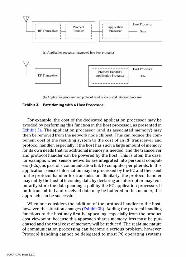
For example, the cost of the dedicated application processor may beavoided by performing this function in the host processor, as presented inExhibit 3a. The application processor (and its associated memory) maythen be removed from the network node chipset. This can reduce the com-ponent cost of the resulting system to the cost of an RF transceiver andprotocol handler, especially if the host has such a large amount of memoryfor its own needs that no additional memory is needed, and the transceiverand protocol handler can be powered by the host. This is often the case,for example, when sensor networks are integrated into personal comput-ers (PCs), as part of a communication link to computer peripherals. In thisapplication, sensor information may be processed by the PC and then sentto the protocol handler for transmission. Similarly, the protocol handlermay notify the host of incoming data by declaring an interrupt or may tem-porarily store the data pending a poll by the PC application processor. Ifboth transmitted and received data may be buffered in this manner, thisapproach can be successful.
When one considers the addition of the protocol handler to the host,however, the situation changes (Exhibit 3b). Adding the protocol handlingfunctions to the host may first be appealing, especially from the productcost viewpoint; because this approach shares memory, less must be pur-chased and the total cost of memory will be reduced. The real-time natureof communication processing can become a serious problem, however.Protocol handling cannot be delegated to most PC operating systems
Exhibit 3. Partitioning with a Host Processor
AU1823_C06.fm Page 124 Monday, July 14, 2003 7:03 AM
©2004 CRC Press LLC
because they usually cannot guarantee protocol timing to the accuracyneeded.
In non-PC implementations, software integration is also made more dif-ficult by the addition of protocol handling, especially if the host is runningother real-time (or near-real-time) processes. This is especially true ofembedded systems, such as those found in PDAs, cellular telephones, andother battery-powered portable devices, which already have strict limitson their computational resources. Interrupt handling and context switch-ing, for example, must be carefully evaluated to ensure that sufficientresources — in the form of RAM, nonvolatile memory, and instructionspeed — are always available for all real-time processes, even in the worst-case scenario when the host processor is most heavily loaded. Becauseeven the identification of the worst-case scenario may be difficult to deter-mine, guaranteeing that resources are always available for multiple real-time processes can be difficult.
At the opposite extreme, a lightly loaded but quite powerful host proces-sor is no panacea either. A powerful host processor that is frequently awak-ened to perform protocol-handling functions may have little trouble meet-ing the real-time requirements of the communication protocol. Unlessspecial care is taken in its design, however, it is likely not to be a power-effi-cient implementation. A system that is lightly loading a powerful host pro-cessor is usually doing so to improve its average power consumption. Thissituation can develop, for example, when the processor is being used toservice a second communication protocol, such as a cellular telephoneprotocol. Because the two protocols have independent timing require-ments, one will interrupt the sleep periods designed into the other. Thiscan result in the processor remaining active almost in perpetuity, and theaverage power consumption of the system rises dramatically.
Faced with these trade-offs, when a host processor is available, a com-promise is often in order. An attractive approach may be to employ a ded-icated protocol handler to off-load the host processor, but use theresources of the host processor for application data processing. This limitsthe timing requirements placed on the host as well as the total amount ofprocessing required (because wireless sensor networks are assumed tohave relatively low data throughput). This approach is also appealing inthat it largely separates the data-generation function from the data-trans-mission function of the node. Legacy wired and wireless systems, for exam-ple, may already have application processing built into their code; employ-ing a dedicated protocol handler enables a wireless sensor network nodeto be constructed with minimal attention paid to the existing applicationcode. Not only does this represent less work that must be done by the soft-ware engineer, it also reduces the possibility that software bugs will beintroduced into the existing code. Often, when faced with the choice
AU1823_C06.fm Page 125 Monday, July 14, 2003 7:03 AM
©2004 CRC Press LLC
between higher memory costs and higher software integration costs (withtheir associated quality concerns), the decision is to purchase memory.
The final partitioning decision concerns the location of the trans-ducer(s). Their location, and the means by which their information is com-municated to the rest of the wireless sensor network node, can be of spe-cial significance to the economic success of the design.
6.3 TRANSDUCER INTERFACES
For a manufacturer of wireless sensor network devices, the transducerinterfaces can be a major economic problem. The manufacturer achievesprofitability by achieving economies of scale (i.e., by manufacturing a largequantity of identical devices). In the electronics industry, this is done bysemiconductor integration, which requires very large sales (on the orderof millions of units) to defray the one-time costs of chip design, mask setgeneration, etc.; however, a nearly infinite variety of sensors and actuatorsare used. How may these be combined in a wireless sensor network prod-uct line so that the manufacturer achieves the sale of a large quantity ofidentical devices?
6.3.1 Integrated Sensors
One way of doing this is by identifying a selection of sensors that are capa-ble of satisfying a substantial portion of the market, then integrating themalong with the wireless sensor network transceiver. If, as is frequently thecase, the associated “actuator” in the application is just an electricalswitch, or information to be stored in RAM or passed on to a host com-puter, the node may be completely integrated. However, this approach hassome difficulties:
•
The sensors may be difficult to integrate
. Ideally, one would like sensorsthat are integratable on the same die as the wireless sensor networktransceiver, for a completely integrated solution; however, even if thisis technically feasible, it may drive the cost of the fabrication processup to the point that it is not practical. An alternative solution is toplace the sensor(s) in separate dice but in the same package as thetransceiver — a method that attains much of the usefulness of total in-tegration, if not all the cost benefits. In any event, many sensors stillcannot be integrated at all.
•
The system is inflexible.
From the user’s standpoint, a purchased net-work node is application-specific; it cannot be used for any other ap-plication. From the manufacturer’s standpoint, if a different sensor isneeded, even one of the same type but differing in specification (accu-racy, response time, etc.), nothing can be done short of designing andmanufacturing a new integrated circuit, a time-consuming and expen-
AU1823_C06.fm Page 126 Monday, July 14, 2003 7:03 AM
©2004 CRC Press LLC
sive task. Because the actuators in this example are either simpleswitches or, in the degenerate case, information itself, it is relativelyeasy to reprogram the nodes to perform multiple functions based onthe information received from the network (e.g., control the switchesin a different manner). Even here, however, significant limitations ex-ist. For example, the voltage and current capabilities of the switches ina completely integrated design will be limited to those compatiblewith a modern digital integrated circuit fabrication process. Thismeans that, unless extraordinary measures are taken, the current willbe limited to a few tenths of an ampere and the voltage to 3.6 V or so.This precludes the node from directly controlling household applianc-es, for example, although a logical output from the node can certainlycontrol a semiconductor switch on a second die (made in a high-cur-rent, high-voltage process) that, in turn, can control a household ap-pliance.
•
Legacy sensors, perhaps those associated with a previously installedwired sensor network, cannot be reused.
In some applications, for exam-ple, sensor networks in nuclear reactors, where access to placed sen-sors is difficult, this is a significant handicap.
Despite this (rather foreboding) list, some integratable sensors may findwide application. One example is a temperature sensor. Making a moder-ately precise and accurate temperature sensor of limited range in an inte-grated circuit is relatively easy; many possible designs are available, mostof which revolve around the temperature dependence of the voltage dropacross a forward-biased silicon diode, typically
-
2 mV/
∞
C.
2
Such a sensormay have wide application in areas as diverse as heating, ventilation, andair conditioning (HVAC) as well as industrial control, where the actuatorcan be a switch controlling a heater in a thermostat, for example, and inhealth monitoring, where the actuator may be a display, or simply datastored in a computer.
In most cases, however, it is not possible to integrate both sensor andactuator in all wireless sensor network nodes used in an application. Thisforces the node to have a transducer interface to the outside world. Thequestion then becomes how to design the interface to achieve the maxi-mum possible market penetration.
6.3.2 The External Interface
An old aphorism states, “If you try to please everyone, no one will like it,”and nowhere is this more true than in the design of an external transducerinterface. The manufacturer must put enough flexibility in the interface tomeet the needs of a large segment of the market, without adding so muchto the node that it becomes economically prohibitive to use in any oneapplication.
AU1823_C06.fm Page 127 Monday, July 14, 2003 7:03 AM
©2004 CRC Press LLC
To start, the manufacturer must decide if the transducer interface is tobe analog or digital. The output of most sensor elements is inherently ana-log, while the wireless sensor network transmits only digital data; there-fore, an analog-to-digital conversion must take place. Similarly, many actu-ators produce an analog output; digital-to-analog conversion is thereforenecessary. Placing analog-to-digital and digital-to-analog converters (ADCsand DACs) on the network node may reduce the total cost of the system,especially if multiple sensors are attached to each node and the converterscan be shared between them. Converters of more than moderate speed,accuracy, and precision are difficult to manufacture on a conventional dig-ital IC process, however, and add power consumption and die area (and,therefore, cost). A manufacturer of wireless sensor network nodes maychoose to reduce the cost of the product by incorporating neither ADCsnor DACs, instead using a digital transducer interface. This requires theuser to employ transducers that have internal (or inherent) ADCs andDACs, which may significantly limit the market of this network nodedesign.
If the decision is to employ a digital transducer interface, the next deci-sion is to decide if the interface will be a completely logical one, or if spe-cial-purpose outputs (essentially very large pad drivers, used as switches,etc.) will be included. The addition of special-purpose outputs may makethe network node capable of stand-alone operation in some high-volumebut low-margin applications (e.g., a wireless light switch), by eliminatingthe need for a second, special-purpose switching transistor in the systemdesign. A node with special-purpose outputs also may be capable of satis-fying some low-volume but high-margin applications (e.g., military sens-ing). The special-purpose outputs can greatly increase the size of the inte-grated circuit, however, driving up costs for those applications that do notuse them. The manufacturer must decide which market is to be addressed.
One compromise is to place a purely logical interface on the networknode IC, but place a second, special-purpose die controlled by the logicalinterface, in the same package. In this way, the network node IC may be pro-duced in high volume, while one of several relatively cheap (and easy todesign and fabricate) special-purpose chips may be mated to it as theapplication requires. This approach offers market flexibility at the cost ofmaking multiple special-purpose chips, and the cost associated with plac-ing multiple chips in the same package. A variation on this theme isemployed by thin-film ceramic module manufacturers, which may use thesame network node IC, but customize each design by modifying the sur-rounding components as needed for the application.
If the manufacturer decides that the transducer interface is to be a com-pletely logical one, decisions must still be made. The first decision is
AU1823_C06.fm Page 128 Monday, July 14, 2003 7:03 AM
©2004 CRC Press LLC
whether the interface should be in series or parallel. This decision hingeson the relative value in the implementation of speed versus size.
A parallel interface (an external bus) has the advantage of speed; witheight data pins, a byte (eight bits) can be transmitted in each clock cycle.Alternatively, at the same data rate, an eight-bit parallel interface may beclocked at one-eighth the clock rate of a serial interface; this may be anadvantage if the interface is a source of RF interference. (However, thelarger number of circuit board traces used by a parallel interface maynegate this advantage.) If the network node contains a microcontroller, themicrocontroller’s general-purpose input/output (GPIO) pins can be effi-ciently used in a parallel interface. In addition, sensors designed for aneight-bit microcontroller bus can be quite common; however, these bene-fits come at some cost. The parallel interface requires ten pins on the net-work node (eight data pins, one clock, and one control or enable pin),which also must be routed to the sensor(s). In very small implementations,routing these lines may be difficult, or require a more expensive multilayercircuit board. In very low-end applications, especially those in which a cus-tom integrated circuit (as opposed to an off-the-shelf microcontroller) isused, the ten pins needed for the sensor interface may double the pincount of the chip. Although the extra pins alone will drive up the productcost (due to the cost of wire bonding and packaging), the die area of thechip may now be pad-limited (i.e., determined by the number of wire bond-ing pads needed around its periphery, instead of by the area of the inte-grated circuits themselves). This will establish a lower limit on the size ofthe chip, regardless of the fabrication process employed.
A serial interface has the advantage of size. With a single data pin (plusone each for the clock and the control or enable pin), a serial interface issmall, with a minimal effect on both chip pad count and circuit board area.This makes it ideal for very small, low-cost products, although it also hasits drawbacks. Because the serial interface trades speed for size, it isslower; a careful analysis should be done to ensure that sufficient data canbe transferred across it under worst-case conditions. These can occur, forexample, in an emergency condition, when the wireless sensor network isrequesting frequent sensor updates or giving frequent commands to anactuator. Several types of serial interfaces are also available on the market,not all of which are compatible. This can be a serious problem when field-replaceable transducers are replaced by those from a different vendor.Often, the interfaces may appear to be compatible, but may differ in somedetail, such as implied addressing (i.e., their behavior when sequentialdata packets are sent to the same address). In addition, some serial inter-faces are proprietary. To avoid these issues, many transducer manufactur-ers do not manufacture products with serial interfaces; this limits the mar-ket of a serial-interface wireless sensor network node (unless an external
AU1823_C06.fm Page 129 Monday, July 14, 2003 7:03 AM
©2004 CRC Press LLC
series-to-parallel converter is employed). Another alternative is the use ofa mixed-mode interface, such as pulse-width modulation. Neither fullyanalog nor fully digital, pulse-width modulation encodes the transferreddata in the duty cycle of a square wave.
Once the series/parallel interface decision is made, the remaining issueis one of selecting speeds and standards. Speeds, when not set by the stan-dard, are usually limited by power, electromagnetic compatibility (EMC),and the application requirements.
Leakage current aside, the power consumed by a switching circuit ele-ment is
P = CV
2
f
where
P
= the power consumed by the switching element (in W)
C
= the capacitance of the element (in F)
V
= the voltage range over which the element is switching (in V)
f
= the frequency of the switching (in Hz)
Because the voltage term is squared, a voltage reduction has the great-est effect on power consumption of an interface. However, to be compati-ble with industry (i.e., available transducers), the selection of availablevoltages is limited to a few choices: 2.7 V, 1.8 V, or, in a few cases, 1.0 V. Thecapacitance is typically unknown to the chip designer. Because the trans-ducer to be used is typically not known (unless the chip is being designedfor a specific transducer), its load capacitance is also not known; to makematters worse, the capacitance of the interface lines between the chip andthe transducer, which can be significant (several tens of picofarads), isunknown as well.
This leaves the frequency of operation as the only parameter over whichthe designer has significant control. To minimize both power consumptionand the potential for the production of electromagnetic interference (seeChapter 9), the designer typically will attempt to minimize the requiredmaximum frequency of operation of the interface, consistent with meetingapplication requirements. The interface capacitance is unknown, there-fore, the designer can only state a maximum total capacitance that the chipwill support (based on the size of the driver circuit on the chip) and themaximum frequency of operation under that condition.
6.4 TIME BASE ACCURACY AND AVERAGE POWER CONSUMPTION
A subtle relationship exists between the accuracy of the time base used ina synchronous communication system, such as a wireless sensor networkemploying beacons, and the minimum attainable power consumption of
AU1823_C06.fm Page 130 Monday, July 14, 2003 7:03 AM
©2004 CRC Press LLC
that network. This relationship develops because of the time uncertaintythat develops between the transmitting and receiving nodes that, in turn,requires the receiving node to be active a larger fraction of time to ensurethat it is active when the message is sent from the transmitting node. Forwireless sensor networks incorporating a relatively short beacon period,for example, this time uncertainty may be negligible when compared withthe receiver warm-up time and the transmission time of the beacon itself.For networks that must employ a longer beacon period to reduce theiraverage power consumption, however, the effects of finite time base accu-racy produces a lower limit on the duty cycle of the receiving device and,therefore, its average power consumption.
The analysis that follows begins by assuming a simple, fixed, differencein period between the time base of the transmitter and receiver; any varia-tion in period (i.e., jitter) is neglected, as is any change in the time baseover time (i.e., drift). Later, the effect of these complicating factors is addedto the model. Further, it is assumed that receiving nodes are capable of syn-chronization to transmitting nodes, so that the beacon timers of receivingnodes are reset upon successful reception of a transmitted beacon, andany timing error between the nodes does not accumulate beyond a singlebeacon period.
Consider a transmitting node with a stated time base accuracy of
e
t
ppm.That is to say, if the desired beacon period is T
1
, the node will transmit bea-cons with a constant period somewhere in the range (T
1
¥
(1
-
e t ), T 1
¥
(1
+
e
t )). If a receiving node has just received a beacon from this transmitter, itsets a timer to wake itself up in time to receive the next beacon. The issueis to determine what value the receiving node should program in its timer,not only because of the transmitter time base error, but also because of thetime base of the receiving node itself is imperfect, with a stated time baseaccuracy of
e
r
ppm. If the receiving node is expecting the next beacon tooccur at time T
1
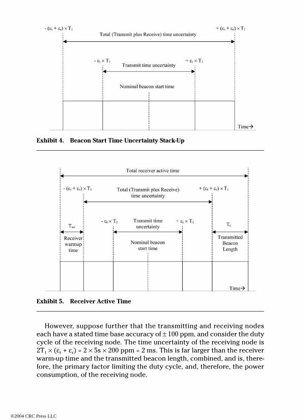
, the situation is as shown in Exhibit 4.
The beacon time uncertainty, as observed by the receiving node, is thesum of both transmitting and receiving node time base uncertainties, plac-ing the beacon in the range (T
1
¥ (1
-
(
e
t
+
e
r
)), T
1
¥
(1
+ (
e
t
+
e
r
))). Note thatthis does not include the time of the actual beacon transmission, T
c
, norany warm-up time associated with the receiver, T
wr
. When these factors areconsidered, the active time required of the receiving node to ensure recep-tion of the transmitted beacon is T
wr
+
2T
1
¥
(
e
t
+
e r
)
+ T
c
, as illustrated inExhibit 5.
As an example, suppose a system were designed to have a beacon trans-mission length of T
c
= 100
m
s and a period of T
1
= 5 s, using hardware thatrequires a warm-up period of T
wt
= 150
m
s prior to each transmission. Thetransmitted duty cycle is then (T
c
+
T
w
)/T
1
= 250
m
s/5 s = 50 ppm.
AU1823_C06.fm Page 131 Monday, July 14, 2003 7:03 AM
©2004 CRC Press LLC
However, suppose further that the transmitting and receiving nodeseach have a stated time base accuracy of
±
100 ppm, and consider the dutycycle of the receiving node. The time uncertainty of the receiving node is2T
1
¥
(
e
t
+
e
r
) = 2
¥
5s
¥
200 ppm = 2 ms. This is far larger than the receiverwarm-up time and the transmitted beacon length, combined, and is, there-fore, the primary factor limiting the duty cycle, and, therefore, the powerconsumption, of the receiving node.
Exhibit 4. Beacon Start Time Uncertainty Stack-Up
Exhibit 5. Receiver Active Time
AU1823_C06.fm Page 132 Monday, July 14, 2003 7:03 AM
©2004 CRC Press LLC
The foregoing analysis is somewhat pessimistic because it overesti-mates the average time the receiving node must be active. Several tech-niques can be employed to reduce this time.
The approach that may come to mind first is to employ a more accuratereference at the receiver (and the transmitter, if possible). This will cer-tainly reduce the time uncertainty at the receiving node; however, themore accurate reference may be expensive, so alternative techniques thatdo not raise hardware costs are preferred.
The first technique recognizes that the receiving node does not have tobe active for the entire time the beacon may be transmitted. It may be putback to sleep once the beacon is received. If this is done, and if the distri-bution of both transmitting and receiving node time base errors is symmet-rical about the desired value (i.e., no systematic offsets), the averageactive time of the receiver is Twr + T1 ¥ (et + er) + Tc; the beacon is receivedon average halfway through the total time uncertainty range at the receiv-ing node. Because the time uncertainty at the receiving node has the larg-est effect on the duty cycle (and, therefore, the power consumption) of thereceiving node, this is a significant improvement. In the example at hand,moving to this algorithm reduces the average receiver active time from2.25 ms to 1.25 ms, a reduction of 44 percent.
A further reduction may be realized by a more sophisticated algorithmat the receiver that attempts to model the effects of inaccuracy of bothtransmitter and receiver time bases. This can be done by recognizing thata high degree of correlation often exists between the apparent periods ofsequential beacons, especially if the jitter of the time base references islow, as is usually the case. Continuing the example, suppose that the timebase of the receiving node is 10 ppm slow. If the time base of the transmit-ting node has no error, the beacon will appear to arrive 10 ppm early to thereceiving node. If the time base of the transmitting node is 50 ppm fast,however, the beacon will appear to arrive 10 + 50 = 60 ppm early; sequen-tial beacon periods will appear to change only as the time references drift— if the time bases of both transmitting and receiving nodes are stable, allreceived beacons will appear to be 60 ppm early. The receiving node mayrecognize this correlation and compensate for it, by modifying the valueprogrammed into its wakeup timer, so that it awakes just prior to the(apparently early) beacon. (This is equivalent to automatic frequency con-trol, that is, to regulating its own time base to that of the transmitter.) Inthis case, the average active time of the receiving node can be reduced toTwr + Tbuffer + Tc, where Tbuffer is a small time buffer that accounts for anypossible drift between the transmitter and receiver time bases during thepreceding beacon period. Such drift may occur, for example, by a temper-ature change of one or both of the node time base references, by a mechan-
AU1823_C06.fm Page 133 Monday, July 14, 2003 7:03 AM
©2004 CRC Press LLC
ical shock to one or both of the references, or other means. Higher-ordermodeling of the drift may be employed, if desired, to minimize Tbuffer.
Note that this algorithm requires a learning period; at first, the receiverdoes not know the relative time base error of the transmitter, and so Tbuffer
must be very large so that a very wide time window is open to ensurereception of the beacon. Once a series of beacons is detected, however,Tbuffer may be greatly reduced and the window significantly narrowed.
Continuing the present example further, if Tbuffer is (arbitrarily and ratherconservatively) set to 50 ms, accounting for a 10 ppm drift between timebases in one beacon period, the average active time of the receiver is Twr +Tbuffer + Tc = 150 ms + 50 ms + 100 ms = 300 ms. The duty cycle of the receivingnode has been reduced from 2.25 ms/5 s = 500 ppm, using the initial unso-phisticated algorithm, to 300 ms/5 s = 60 ppm, an improvement of 88 per-cent. Because the active power consumption can be three orders of magni-tude greater than the sleep power consumption, this represents asignificant average power consumption savings.
From this analysis, it is clear that to attain very low duty cycles and,therefore, very low average power consumption in receiving nodes, thedesign of the time bases used by both transmitter and receiver, as well asthe design of the timing algorithm used by the receiver, are of criticalimportance, especially in systems requiring minimum implementationcost.
An interesting strategy to minimize both duty cycle and implementationcost is to specify a maximum any time reference value in the network of thedrift allowed during one beacon period. Note that this is slightly differentthan a simple time base accuracy specification; a time base accuracy spec-ification considers the time base error from a desired value, while a driftspecification considers the change in time base error between consecutivebeacon periods. This is done in the Bluetooth™ specification, for example.The strategy here is to enable the use of untuned or uncompensated refer-ence elements to minimize the product cost, while still enabling receivingnodes to track transmitting nodes (by limiting how much they may driftwithin a beacon period). Interestingly, there are bounds over which thistype of specification is useful: for very short beacon periods, any possibledrift is negligible, while for very long beacon periods, the drift specificationmay be more strict than the time base accuracy specification. For example,one may specify a maximum reference drift of 10 ms and a reference accu-racy of 100 ppm. For a beacon period greater than 10 s, the drift specifica-tion is the more stringent. This is especially significant in wireless sensornetworks, which may have lengthy beacon periods, but the nodes of whichmay be very small, with low thermal inertia. With such devices, a change oftemperature may be reflected in the reference within one beacon period.
AU1823_C06.fm Page 134 Monday, July 14, 2003 7:03 AM
©2004 CRC Press LLC
Because of these considerations, a time base drift specification should becarefully evaluated by the system designer to ensure its usefulness and toavoid unintended consequences.
6.5 CONCLUSION
The design of wireless sensor network nodes has a larger effect on the eco-nomic potential of the resulting network than does the design of nodes fornetworks containing infrastructure, such as a cellular telephone network.This is because, although the cost of nodes in the telephone network maybe justified by the value of the network provided by the infrastructure, thevalue of a wireless sensor network is determined solely by the nodes them-selves. Node implementation is, therefore, of primary importance in thedesign of a successful wireless sensor network.
The partitioning decisions that must be made at the start of a wirelesssensor network design effort are complex, and involve market forces, tech-nological capabilities, and organization strategy and business relation-ships; there is likely a market for which every possible partition is optimal.The task facing the designer, then, is to ensure that the partition chosen issuitable for the market at hand. Often, the goal is to achieve utility in asmany markets as possible, to maximize return on the engineering designtime invested; this multiple-market requirement only adds to the difficultyof the partitioning decision. In addition to the components of the commu-nication transceiver itself, the designer must consider the presence of anyhost processor, which may affect hardware/software trade-offs, the type ofpower source(s) available, and the type of interface(s) needed to commu-nicate with sensors and actuators.
One important but often overlooked factor in the design of wireless sen-sor network nodes is the effect finite stability of the node time base has onthe minimum attainable duty cycle, and, therefore, the minimum attainableaverage power consumption, of the network node. The resulting trade-offbetween the cost of the node time base and the attainable life of the battery(or other power source) must be made properly to achieve the desiredmarket success.
References
1. Institute of Electrical and Electronics Engineers, Inc., IEEE Std. 802.15.4-2003, IEEEStandard for Information Technology — Telecommunications and Information Ex-change between Systems — Local and Metropolitan Area Networks — Specific Re-quirements — Part 15.4: Wireless Medium Access Control (MAC) and Physical Layer(PHY) Specifications for Low Rate Wireless Personal Area Networks (WPANs). NewYork: IEEE Press. 2003.
2. Paul R. Gray and Robert G. Meyer, Analysis and Design of Analog Integrated Circuits,3rd ed. New York: John Wiley & Sons. 1993. p. 16.
AU1823_C06.fm Page 135 Monday, July 14, 2003 7:03 AM
©2004 CRC Press LLC