Embed Size (px)
Citation preview

Berkeley
Wireless Receiver Architectures
Prof. Ali M. Niknejad and Dr. Osama Shana’a
U.C. BerkeleyCopyright c© 2014 by Ali M. Niknejad
Niknejad Advanced IC’s for Comm

Outline
Review of key receiver specs
Complex baseband equivalent of a bandpass signal
Superheterodyne
Image Rejection Architectures
Direct-conversion
References
Niknejad Advanced IC’s for Comm

Review of Receiver Specifications
Niknejad Advanced IC’s for Comm

Receiver Specifications
Sensitivity, the weakest signal that can be detected by areceiver. Set by amount of Amplificaiton and Noise
Selectivity, or the ability to select one frequency band in thepresence of interfering signals in nearby frequency bands.Determined by the amount of Filtering and the receiverLinearity
Dynamic Range, or the linear range of a receiver signal thatcan be processed with minimal impact on the detection biterror rate (BER), related to the Linearity and Noise in thereceiver. Greatly improved with Variable Gain Control (orProgrammable Gain Control)
Niknejad Advanced IC’s for Comm

Receiver Goal #1: Amplification
ADCLNA
A detector works well with a fairly strong signal. For instance, if theinput referred noise/offset/LSB is 10’s mV, the input signal shouldbe 10X or more larger.
The weakest signals can be -100 dBm or lower, so a gain of > 90dBmay be needed. What happens when the input signal is 0 dBm???
In gaining up the signal, we have to keep the noise and distortionsmall relative to the signal power in order to meet the requiredSNDR.
SDR Concept (minimize RF gain): ADC spec of > 100dB ofdynamic range (> 17bit) with a sampling frequency of 2fRF .
Niknejad Advanced IC’s for Comm

Receiver Goal #2: Variable Amplification
ADCLNA VGA
Since the received power can vary greatly in dynamic range fromvery weak levels (-110 dBm) to fairly strong signals (0 dBm), thereceiver should ideally have variable gain of ∼ 0-100 dB.
Without variable gain, the dynamic range of a receiver is limitedsince the detector or ADC may have a limited range. For an ADC,it’s roughly 6 dB/bit, and the power consumption growsexponentially with the number of bits.
Variable gain at RF is difficult. But even if implemented, thesensitivity would be limited by the presence of interfering signals.
Niknejad Advanced IC’s for Comm

Receiver Goal #3: Freq. Translation
ADCLNA VGA
As the carrier frequency and the information signal are at verydisparate frequencies (say 1 GHz versus 1 MHz), we requiremodulation and demodulation.Also, we prefer to work at lower frequencies to save power.We would like to frequency translate our signal to “baseband”and perform filtering/gain rather than at RF. This means weshould “mix” the signal as soon as possible.We shall see that mixers are prone to frequency translatemany different frequencies to the same “IF”, and so they arerelatively noisy and require image rejection (NF ∼ 10 dB). Wemust precede the mixers with a low noise amplifier (LNA) toovercome this noise.
Niknejad Advanced IC’s for Comm

Receiver Goals #4: Filtering
ADCLNA VGA
Imagine trying to receive a signal at a power of -100 dBm inthe presence of an inband“jammer” or interference signal withpower -40 dBm.We would like to set the gain at 100 dB, but this wouldseverly compress the receiver due to the jammer.We must therefore apply a sharp filter to remove the jammingsignal before we apply all the gain.If these jammers (blockers/interferers) are not attenuated,they tend to reduce the gain of the signal (P−1dB), increasethe noise figure of the receiver (through mixing noise in otherbands to the same IF, especially phase noise), and produceintermodulation products that fall in band and reduce thesensitivity of a receiver
Niknejad Advanced IC’s for Comm

Filtering in Receivers
VCO
LNA
VGA
ADC
Niknejad Advanced IC’s for Comm

Receiver Summary
ADC
LNA
+-
+
ADC+-
+
LO_I
LO_Q
I
Q
High gain required to meet sensitivity (∼ 70dB)
DC offset cancellation is a must (due to mismatches)
Gain control to accommodate strong blockers
High linearity filtering stages to knock down blockers
Image rejection and harmonic rejection (cannot be filteredeasily)
Tunable baseband IF corner frequency (200 kHz 100 MHz)for different standards
Niknejad Advanced IC’s for Comm
Complex Baseband Representation
Niknejad Advanced IC’s for Comm

Complex Baseband
Any passband waveform can be written in the following form:
sp(t) = a(t) cos [ωct + θ(t)]
sp(t) = a(t) cosωct cos θ(t)− a(t) sinωct sin θ(t)
sp(t) =√
2sc(t) cosωct −√
2ss(t) sinωct
sc(t) , a(t) cos θ(t) = I (t)
ss(t) , a(t) sin θ(t) = Q(t)
a(t) = |s(t)| =√
s2c (t) + s2
s (t)
θ(t) = tan−1 ss(t)
sc(t)
Niknejad Advanced IC’s for Comm

Complex Baseband (cont)
We define the complex baseband signal and show that alloperations at passband have a simple equivalent at complexbaseband:
s(t) = sc(t) + jss(t) = I (t) + jQ(t)
sp(t) = Re{√
2s(t)e jωc t}
||s||2 = ||sp||2
Niknejad Advanced IC’s for Comm

Orthogonality
An important relationship is the orthogonality between themodulated I and Q signals: < xc , xs >=< Xc ,Xs >= 0
This can be proved as follows (Parseval’s Relation):
< Xc ,Xs >=
∫ ∞−∞
Xc(f )X ∗s (f )df
xc(t) =√
2sc(t) cosωct xs(t) =√
2ss(t) sinωct
xc(t) =1√2
(sc(t)e jωc t + sc(t)e−jωc t)
Xc(f ) =1√2
(Sc(f − fc) + Sc(f + fc))
Xs(f ) =1√2j
(Ss(f − fc)− Ss(f + fc))
Niknejad Advanced IC’s for Comm

Orthogonality
< Xc ,Xs >=
1
2j
∫ ∞−∞
((Sc(f − fc) + Sc(f + fc))× (S∗s (f − fc)− S∗s (f + fc))) df
In the above integral, if the carrier frequency is larger than thesignal bandwidth, then the frequency shifted signals do notoverlap
Sc(f − fc)S∗s (f + fc) ≡ 0
Sc(f + fc)S∗s (f − fc) ≡ 0
< Xc ,Xs >=1
2j
[∫ ∞−∞
Sc(f − fc)S∗s (f − fc)df −∫ ∞−∞
Sc(f + fc)S∗s (f + fc)df
]
< Xc ,Xs >=1
2j
[∫ ∞−∞
Sc(f )S∗s (f )df −∫ ∞−∞
Sc(f )S∗s (f )df
]= 0
Niknejad Advanced IC’s for Comm
Complex Baseband Spectrum
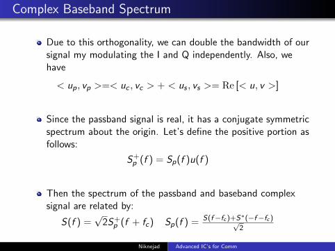
Due to this orthogonality, we can double the bandwidth of oursignal my modulating the I and Q independently. Also, wehave
< up, vp >=< uc , vc > + < us , vs >= Re [< u, v >]
Since the passband signal is real, it has a conjugate symmetricspectrum about the origin. Let’s define the positive portion asfollows:
S+p (f ) = Sp(f )u(f )
Then the spectrum of the passband and baseband complexsignal are related by:
S(f ) =√
2S+p (f + fc) Sp(f ) = S(f−fc )+S∗(−f−fc )√
2
Niknejad Advanced IC’s for Comm

Proof
Proof:
v(t) =√
2s(t)e jωc t
V (f ) =√
2S(f − fc)
Sp(t) = Re(v(t)) =v(t) + v(t)∗
2
Sp(f ) =V (f ) + V ∗(−f )
2=
S(f − fc) + S∗(−f − fc)√2
Niknejad Advanced IC’s for Comm

The Image Problem
LNA
LO
IF IFIF
mr (t) cos(ωLO+ωIF )t×cos(ωLO)t =1
2mr (t) (cos(2ωLO + ωIF )t + cos(ωIF )t)
mi (t) cos(ωLO−ωIF )t×cos(ωLO)t =1
2mi (t) (cos(2ωLO − ωIF )t + cos(ωIF )t)
After low-pass filtering the mixer output, the IF is given by
IFoutput =1
2(mi (t) + mr (t)) cos(ωIF )t
Niknejad Advanced IC’s for Comm

Image Problem (Freq Dom)
IF−IF LO−LO
IF−IF LO−LO
Positive Freq Exp Modulation
Negative Freq Exp Modulation
IF−IF LO−LO
Cosine Modulation
e+jωt
e−jωt
e+jωt
e−jωt
Complex modulation shifts in only one direction . . . realmodulation shifts up and down
Niknejad Advanced IC’s for Comm

Superheterodyne Architecture
Niknejad Advanced IC’s for Comm

Superheterodyne
LNA
O� chip
PassiveBPF
ImageFilter
IFFilter
The choice of the IF frequency dictated by:
If the IF is set too low, then we require a very high-Q imagereject filter, which introduces more loss and therefore highernoise figure in the receiver (not to mention cost).If the IF is set too high, then subsequent stages consume morepower (VGA and filters)Typical IF frequency is 100-200 MHz.
Niknejad Advanced IC’s for Comm

LO Planning in Superhet
LNA
O� chip
PassiveBPF
ImageFilter
IFFilter
PLL1
LO1
PLL2LO2
I
Q
Two separate VCOs and synthesizers are used. The IF LO is fixed,while the RF LO is variable to down-convert the desired channel tothe passband of the IF filter (SAW). This typically results in a 3-4chip solution with many off-chip components.
LO1 should never be made close to an integer multiple of LO2 forany channel. The Nth harmonic of the the fixed LO2 could leak intothe RF mixer and cause unwanted mixing.
IF
IF
LO2 LO1
n LO2
IF
nLO2 leaks into RF mixer
Niknejad Advanced IC’s for Comm

The 1/2 IF Problem
IF
LO
IF
½ IF
Assume that there is a blocker half-way between the LO and thedesired channel. Due to second-order non-linearity in the RFfront-end:[
mblocker (t) cos(ωLO +1
2ωIF )t
]2
= m2blocker (t)
1 + cos(2ωLO + ωIF )t
2
If the LO has a second-order component, then this signal will foldright on top of the desired signal at IF:
[m2
blocker (t) cos(2ωLO + ωIF )t]
cos(2ωLO)t = m2blocker (t) cos(ωIF )t + · · ·
Note: Bandwidth expansion of blocker due to squaring operation.Niknejad Advanced IC’s for Comm

Half-IF Continued
IF
DC
½ IF
IF
DC
½ IF
If the IF stage has strong second-order non-linearity, then thehalf-IF problem occurs through this mechanism:
2
[mblocker (t) cos(
1
2ωIF )t
]2
= m2blocker (t) + m2
blocker (t) cos(ωIF )t
This highlights the importance of frequency planning. Oneshould select the IF by making sure that there is no stronghalf-IF blocker. If one exists, then the second-ordernon-linearity must be carefully managed.
Niknejad Advanced IC’s for Comm

Secondary Image Issue
LO1 RFIF1LO2IM2IF2 IM2’DC
When we down-convert twice using a mixer, we have to makesure that the image in both the image bands is suppressed.The secondary mixer has an image that may fall in a bandclose to our desired signal, making the second image rejectiondifficult.
IM2 = IF1 − 2IF2 = IF1 − 2(IF1 − LO2) = −IF1 + 2LO2
IM ′2 = IM2 + LO1 = LO1 + 2LO2 − IF1
= LO1 + 2LO2 − (RF − LO1) = 2(LO1 + LO2)− RF
Note LO1 + LO2 = RF − IF2
IM ′2 = 2RF − 2IF2 − RF = RF − 2IF2
Niknejad Advanced IC’s for Comm

Dual-Conversion Single-Quad
LNA
O� chip
PassiveBPF
ImageFilter
IFFilter
PLL1
LO1
PLL2LO2
I
Q
Disadvantages:
Requires bulky off-chip SAW filtersAs before, two synthesizers are requiredTypically a three chip solution (RF, IF, and Synth)
Advantages:
Robust. The clear choice for extremely high sensitivity radiosHigh dynamic range SAW filter reduces/relaxes burden onactive circuits. This makes it much easier to design the activecircuitry.By the same token, the power consumption is lower
Niknejad Advanced IC’s for Comm

Image Reject Architectures
Niknejad Advanced IC’s for Comm

Complex Mixer
+
+
+
–
+
+
y = x ·z = (xr+jxi )·(zr+jzi )
yi = xizr + xrzi
yr = xrzr − xizi
y(t) = e jω0tx(t)
Y (ω) = X (ω − ω0)
A complex mixer is derived by simple substitution.
Note that a complex exponential only introduces a frequencyshift in one direction (no image rejection problems).
Niknejad Advanced IC’s for Comm

Hilbert Architecture
+90◦
IF
90◦
A
B
C
LNA
Image suppression by proper phase shifting.RF = mr (t) cos(ωLO + ωIF )t + mi (t) cos(ωLO − ωIF )t
A = RF×cos(ωLO t) =1
2mr (t) (cos(2ωLO + ωIF )t + cos(ωIF )t)+
1
2mi (t) (cos(2ωLO − ωIF )t + cos(ωIF )t)
B = RF×sin(ωLO t) =1
2mr (t) (sin(2ωLO + ωIF )t − sin(ωIF )t)+
1
2mi (t) (sin(2ωLO − ωIF )t + sin(ωIF )t)
C =1
2mr (t) (− cos(2ωLO + ωIF )t + cos(ωIF )t) +
1
2mi (t) (− cos(2ωLO − ωIF )t − cos(ωIF )t)
IF+ = A + C = mr (t) cos(ωIF t)
IF− = A− C = mi (t) cos(ωIF t)
Niknejad Advanced IC’s for Comm

Sine/Cosine Together
IF!IF LO!LO
IF!IF LO!LO
Cosine Modulation
Sine Modulation
IF!IF LO!LO
Delayed Sine Modulation
!/j
!/j!/j
!/j
Since the sine treats positive/negative frequencies differently(above/below LO), we can exploit this behavior
A 90◦ phase shift is needed to eliminate the image
90◦ phase shift equivalent to multiply by −jsign(f )
Niknejad Advanced IC’s for Comm

Hilbert Implementation
Advantages:
Remove the external image-reject SAW filterBetter integration
Requires extremely good matching of components (pathsgain/phase). Without trimming/calibration, only ∼40dBimage rejection is possible. Many applications require 60dB ormore.
Power hungry (more mixers and higher cap loading).
Note: A realimplementation uses45◦/135◦ phaseshifters for bettermatching/tracking.
+
135◦
IF
A
B
C
45◦
135◦
45◦
D
LNA
Niknejad Advanced IC’s for Comm

Gain/Phase Imbalance
A = RF × (1 + α) cos(ωLO t +φ
2) =
12mr (t)(1 + α)
(cos(2ωLO t + ωIF t + φ
2) + cos(ωIF t −
φ2
))
+
12mi (t)(1 + α)
(cos(2ωLO t − ωIF t + φ
2) + cos(ωIF t + φ
2))
B = RF × (1− α) sin(ωLO t −φ
2) =
12mr (t)(1− α)
(sin(2ωLO t + ωIF t −
φ2
)− sin(ωIF t −φ2
))
+
12mi (t)(1− α)
(sin(2ωLO t − ωIF t −
φ2
) + sin(ωIF t −φ2
))
C =
12mr (t)(1− α)
(− cos(2ωLO t + ωIF t −
φ2
) + cos(ωIF t −φ2
))
+
12mi (t)(1− α)
(− cos(2ωLO t − ωIF t −
φ2
)− cos(ωIF t −φ2
))
IF = A + C =mr (t)
2
((1 + α) cos(ωIF t −
φ
2) + (1− α) cos(ωIF t +
φ
2)
)+
mi (t)
2
((1 + α) cos(ωIF t +
φ
2)− (1− α) cos(ωIF t −
φ
2)
)
IF = mr (t)
[cos(ωIF t) cos(
φ
2)− α sin(ωIF t) sin(
φ
2)
]+ mi (t)
[α cos(ωIF t) cos(
φ
2)− sin(ωIF t) sin(
φ
2)
]
Niknejad Advanced IC’s for Comm

Image-Reject Ratio
IR(dB) = 10 log
(cos φ
2 − α sin φ2
α cos φ2 + sin φ
2
)2
IR ≈=α2 + φ2
4
0 1 2 3 4
0
2
4
6
8
10
Level of image rejection depends on amplitude/phasemismatch
Typical op-chip values of 30-40 dB achieved (< 5◦, < 0.6dB)
Niknejad Advanced IC’s for Comm

RF/IF Phase Shift, Fixed LO
+
90◦
IF
90◦A
B
LNA
A’
RF
RF’
–
RF = mr (t) cos(ωLO + ωIF )t + mi (t) cos(ωLO − ωIF )t
RF ′ = −mr (t) sin(ωLO + ωIF )t − mi (t) sin(ωLO − ωIF )t
A = RF×cos(ωLO t) = 12 mr (t) (cos(2ωLO + ωIF )t + cos(ωIF )t)+ 1
2 mi (t) (cos(2ωLO − ωIF )t + cos(ωIF )t)
A′LPF = −mr (t) sin(ωIF t)− mi (t) sin(ωIF t)
B = RF ′×cos(ωLO t) = 12 mr (t) (− sin(2ωLO + ωIF )t + sin(ωIF )t)+ 1
2 mi (t) (− sin(2ωLO − ωIF )t − sin(ωIF )t)
IF+ = B − A′ = mr (t) sin(ωIF t)
This requires a 90◦ phase shift across the band. It’s mucheasier to shift the phase of a single frequency (LO). Eventhough the LO is variable, it’s a narrowband signal.
Polyphase filters can be used to do this, but a broadbandimplementation requires many stages (high loss)
Niknejad Advanced IC’s for Comm

Weaver Architecture
+90◦ 90◦
IF
A
B
LNARF
C
D
LO1 LO2 –
+
RF = mr (t) cos(ωLO1+ ωIF1
)t + mi (t) cos(ωLO1− ωIF1
)t
IF1 = LO1 − RF
IF = LO2 − IF1 = LO2 − LO1 + RF = RF − (LO1 − LO2)
Eliminates the need for a phase shift in the signal path. Easier to implement phase shift inthe LO path.Can use a pair of quadrature VCOs. Requires 4X mixers!Sensitive to second image.
ALPF = cosωLO1t × RF =
mr
2cos(ωIF1
)t +mi
2cos(ωIF1
)t
BLPF = sinωLO1t × RF = −mr
2sin(ωIF1
)t +mi
2sin(ωIF1
)t
CLPF = A× cosωLO2t =mr
4cos(ωIF )t +
mi
4cos(ωIF )t
DLPF = B × sinωLO2t = −mr
4cos(ωIF )t +
mi
4cos(ωIF )t
IF = C − D =mr
2cosωIF t
Niknejad Advanced IC’s for Comm

Direct Conversion Architecture
Niknejad Advanced IC’s for Comm

Direct Conversion (Zero-IF)
LNA
LO
RFDC
DCωRF = ωLO = ω0
mr (t) cos(ωRF )t × cos(ωLO)t =1
2mr (t) (1 + cos(2ω0)t)
The most obvious choice of LO is the RF frequency, right?IF = LO − RF = DC ?
Why not?
Even though the signal is its own image, if a complexmodulation is used, the complex envelope is asymmetric andthus there is a “mangling” of the signal
Niknejad Advanced IC’s for Comm

Direct Conversion (cont)
90◦
LNA
I
Q
Use orthogonal mixing to prevent signal folding and retainboth I and Q for complex demodulation (e.g. QPSK or QAM)
Since the image and the signal are the same, the image-rejectrequirements are relaxed (it’s an SNR hit, so typically 20-25dB is adequate)
Niknejad Advanced IC’s for Comm

Problems with Zero-IF
LO = p(t) cos(ωLO t + φ(t))
LO×LO = p(t)2+p(t)2 cos(2ωLO t+2φ(t))
DC
Dynamic DC O�set
90◦
LNA
I
Q
Self-mixing of the LO signal is a big concern.
LO self-mixing degrades the SNR. The signal that reflectsfrom the antenna and is gained up appears at the input of themixer and mixes down to DC.
If the reflected signal varies in time, say due to a changingVSWR on the antenna, then the DC offset is time-varying
Niknejad Advanced IC’s for Comm
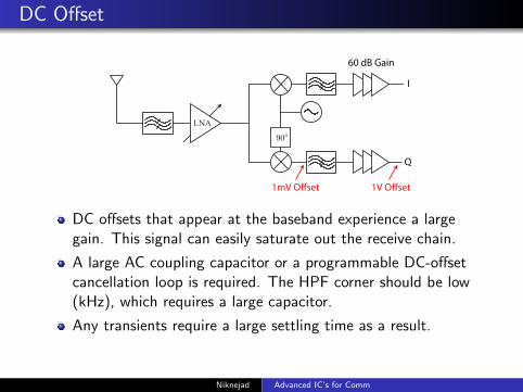
DC Offset
90◦
LNA
I
Q
60 dB Gain
1mV O�set 1V O�set
DC offsets that appear at the baseband experience a largegain. This signal can easily saturate out the receive chain.
A large AC coupling capacitor or a programmable DC-offsetcancellation loop is required. The HPF corner should be low(kHz), which requires a large capacitor.
Any transients require a large settling time as a result.
Niknejad Advanced IC’s for Comm

Sensitivity to 2nd Order Disto
Assume two jammers have a frequency separation of ∆f :
s1 = m1(t) cos(ω1t)
s2 = m2(t) cos(ω1t + ∆ωt)
(s1 + s2)2 = (m1(t) cosω1t)2 + (m2(t) cosω2t)2+
2m1(t)m2(t) cos(ω1t) cos(ω1 + ∆ω)t
LPF{(s1 + s2)2} = m1(t)2 + m2(t)2 + m1(t)m2(t) cos(∆ω)t
The two produce distortion at DC. The modulation of thejammers gets doubled in bandwidth.
If the jammers are close together, then their inter-modulationcan also fall into the band of the receiver.
Even if it is out of band, it may be large enough to saturatethe receiver.
Niknejad Advanced IC’s for Comm

Sensitivity to 1/f Noise
Since the IF is at DC, any low frequency noise, such as 1/fnoise, is particularly harmful.CMOS has much higher 1/f noise, which requires carefuldevice sizing to ensure good operation.Many cellular systems are narrowband and the entirebaseband may fall into the 1/f regime!Example: GSM has a 200 kHz bandwidth. Suppose that theflicker corner frequency is 100 kHz. The in-band noisedegradation is thus:
Noise Density
1/f Slope, 20dB/dec
1kHz
10 kHz
100 kHz
200 kHz
ni2
100 ni2 v2
ave =1
200kHz
∫ 100kHz
1kHz
a
fdf +
∫ 200kHz
100kHz
bdf
a = 1kHz · 100 · v2i
b = v2i
v2ave =
1
200kHz
[a ln
100k
1k+ b(200k− 100k)
]=
1
200kHz(11.5a + 100kb) = 6.25v2
i
Niknejad Advanced IC’s for Comm

Zero-IF Summary
DC offset and flicker noise a major concern. In addition to thedominant mechanisms described earlier, other source of DCoffset include:
Strong blocker signal can leak into mixers and self-mixNon 50% duty cycle of LO can cause output DC offset
Second order distortion a major concern and requires linearLNA/mixer.
Despite these limitations, the zero-IF has many advantages,such as elimination of the image rejection problem and theelimination of all external SAW filters. This has made it avery popular choice.
Niknejad Advanced IC’s for Comm

Low-IF and Double Conversion Architectures
Niknejad Advanced IC’s for Comm

Low IF Architecture
90◦
LNA
I
Q
Com
plex
Imag
eRe
ject
Filt
er
Instead of going to DC, go a low IF, low enough so that theIF circuitry and filters can be implemented on-chip, yet highenough to avoid problems around DC (flicker noise, offsets,etc). Typical IF is twice the signal bandwidth.
The image is rejected through a complex filter. Polyphasefilters are popular choices.
Niknejad Advanced IC’s for Comm

Sliding IF
LNA
Q
÷
cos(ω1t)
sin(ω2t)
cos(ω2t)
ω2 =ω1
N
I
Designing a receiver with two separate frequency synthesizers(PLL’s) that are not integer related requires double thehardware and may suffer from frequency pulling (interaction).Derive second LO by dividing first:
ωRF = ω1 + ω2 = ω1
(1 +
1
N
)This architecture is the sliding IF receiver, so called becausethe IF frequency is not fixed but moves.
Niknejad Advanced IC’s for Comm
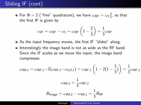
Sliding IF (cont)
For N = 2 (“free” quadrature), we have ωRF = ω132 , so that
the first IF is given by
ωIF = ωRF − ω1 = ωRF
(1− 2
3
)=
1
3ωRF
As the input frequency moves, the first IF “slides” along.
Interestingly the image band is not as wide as the RF band.Since the IF scales as we move the input, the image bandcompresses:
ωIM,1 = ωRF ,1−2(ωRF ,1−ωLO,1) = ωRF ,1
(1− 2(1− 2
3)
)=
1
3ωRF ,1
ωIM,2 =1
3ωRF ,2
BImage = ωIM,2 − ωIM,1 =1
3BRF
Niknejad Advanced IC’s for Comm

Double-Conversion Double-Quad
90◦
÷
90◦
+
+
+
–
+
+
I
Q
A
B
C
D
E
F
LNA
The dual-conversion double-quad architecture has theadvantage of de-sensitizing the receiver gain and phaseimbalance of the I and Q paths.
Niknejad Advanced IC’s for Comm

Analysis of Double/Double
Assuming ideal quadrature and no gain errors:
RF = mr (t) cos(ωLO1 + ωLO2 + ωIF )t + mi (t) cos(ωLO1 + ωLO2 − ωIF )t+
A = LPF{RF × cos(ωLO1t)} =1
2
{mr (t) cos(ωLO2 + ωIF )t+mi (t) cos(ωLO2 − ωIF )t
B = LPF{RF × sin(ωLO1t)} =1
2
{−mr (t) sin(ωLO2 + ωIF )t−mi (t) sin(ωLO2 − ωIF )t
C = LPF{A× cos(ωLO2t)} =1
2
{mr (t) cos(ωIF )t+mi (t) cos(ωIF )t
D = LPF{A× sin(ωLO2t)} =1
2
{mr (t) sin(ωIF )t+−mi (t) sin(ωIF )t
E = LPF{B × cos(ωLO2t)} =1
2
{mr (t) sin(ωIF )t+−mi (t) sin(ωIF )t
F = LPF{B × sin(ωLO2t)} =1
2
{−mr (t) cos(ωIF )t+−mi (t) cos(ωIF )t
I = C − F = (mr (t) + mi (t)) cos(ωIF )t
Q = D + E = (mr (t)− mi (t)) sin(ωIF )t
Niknejad Advanced IC’s for Comm
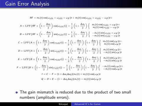
Gain Error Analysis
RF = mr (t) cos(ωLO1 + ωLO2 + ωIF )t + mi (t) cos(ωLO1 + ωLO2 − ωIF )t+
A = LPF{RF ×(
1 +∆a1
2
)cos(ωLO1t)} =
1
2
(1 +
∆a1
2
){mr (t) cos(ωLO2 + ωIF )t+mi (t) cos(ωLO2 − ωIF )t
B = LPF{RF ×(
1−∆a1
2
)sin(ωLO1t)} =
1
2
(1−
∆a1
2
){−mr (t) sin(ωLO2 + ωIF )t−mi (t) sin(ωLO2 − ωIF )t
C = LPF{A×(
1 +∆a2
2
)cos(ωLO2t)} =
1
2
(1 +
∆a1
2
)(1 +
∆a2
2
){mr (t) cos(ωIF )t+mi (t) cos(ωIF )t
D = LPF{A×(
1−∆a2
2
)sin(ωLO2t)} =
1
2
(1 +
∆a1
2
)(1−
∆a2
2
){mr (t) sin(ωIF )t+−mi (t) sin(ωIF )t
E = LPF{B ×(
1 +∆a2
2
)cos(ωLO2t)} =
1
2
(1−
∆a1
2
)(1 +
∆a2
2
){mr (t) sin(ωIF )t+−mi (t) sin(ωIF )t
F = LPF{B ×(
1−∆a2
2
)sin(ωLO2t)} =
1
2
(1−
∆a1
2
)(1−
∆a2
2
){−mr (t) cos(ωIF )t+−mi (t) cos(ωIF )t
I = C − F = (1 + ∆a1∆a2)(mr (t) + mi (t)) cos(ωIF )t
Q = D + E = (1− ∆a1∆a2)(mr (t)− mi (t)) sin(ωIF )t
The gain mismatch is reduced due to the product of two smallnumbers (amplitude errors).
Niknejad Advanced IC’s for Comm

Phase Error Analysis
RF = mr (t) cos(ωLO1 + ωLO2 + ωIF )t + mi (t) cos(ωLO1 + ωLO2 − ωIF )t+
A = LPF{RF × cos(ωLO1t + φ1)} =1
2
{mr (t) cos(ωLO2 + ωIF + φ1)t+mi (t) cos(ωLO2 − ωIF + φ1)t
B = LPF{RF × sin(ωLO1t − φ1)} =1
2
{−mr (t) sin(ωLO2 + ωIF − φ1)t−mi (t) sin(ωLO2 − ωIF − +φ1)t
C = LPF{A× cos(ωLO2t + φ2)} =1
2
{mr (t) cos(ωIF + φ1 + φ2)t+mi (t) cos(ωIF + φ1 + φ2)t
D = LPF{A× sin(ωLO2t − φ2)} =1
2
{mr (t) sin(ωIF − φ1 − φ2)t+−mi (t) sin(ωIF − φ1 − φ2)t
E = LPF{B × cos(ωLO2t + φ2)} =1
2
{mr (t) sin(ωIF + φ1 + φ2)t+−mi (t) sin(ωIF + φ1 + φ2)t
F = LPF{B × sin(ωLO2t − φ2)} =1
2
{−mr (t) cos(ωIF − φ1 − φ2)t+−mi (t) cos(ωIF − φ1 − φ2)t
I = C − F = (mr (t) + mi (t)) cos(φ1 + φ2) cos(ωIF t)
Q = D + E = (mr (t)− mi (t)) cos(φ1 + φ2) sin(ωIF )t
cos(φ1 + φ2) ≈(
1−(φ1 + φ2)2
2
)
The phase error impacts the I/Q channels in the same way,and as long as the phase errors are small, it has a minimalimpact on the gain of the I/Q channels.
Niknejad Advanced IC’s for Comm

Double-Quad Low-IF
90◦
90◦
+
+
+
–
+
+
I
Q
A
B
C
D
LNA
Essentially a complex mixer topology. Mix RF I/Q with LOI/Q to form baseband I/Q
Improved image rejection due to desensitization to quadraturegain and phase error.
Niknejad Advanced IC’s for Comm
References
1 Fundamental of Digital Communication, U. Madhow,Cambridge 2008 O. Shanaa, EECS 290C Course Notes, 2005.
2 A.A. Abidi, “Radio frequency integrated circuits for portablecommunications,” Proc. of CICC, pp. 151-158, May 1994.
3 A.A. Abidi, “Direct conversion radio transceivers for digitalcommunications,” Proc. of ISSCC, pp. 186-187, Feb. 1995.
4 J. Crols and M. Steyaert, “A single-chip 900MHz receiverfront-end with high performance low-IF topology,” IEEEJSSC, vol. 30, no. 12, pp. 1483-1492, Dec. 1995.
5 B. Razavi, RF Microelectronics, Prentice Halls, 1998. J. Crols,M. Steyaert, CMOS Wireless Transceiver Design, KluwerAcademic Publishers, 1997.
6 Practical RF System Design, Willian F. Egdan, Wiley-IEEEPress, 2003.
Niknejad Advanced IC’s for Comm