Embed Size (px)
Citation preview

Wireless Power Transmitter for up to 5W Applications
P9235A-RB Datasheet
© 2021 Renesas Electronics Corporation 1 November 9, 2021
CSP
CSN
VIN
PeakDetector
VDEM
Coil A
ssem
bly
P9235A-RB
SW_S
LDO33
LDO18
PREG
GPIO
A6
LED1
LED2
VIN_LDO
RSNS
GH_BRG1
SW_BRG1
GL_BRG1
GH_BRG2
SW_BRG2
GL_BRG2M ISOMOSI
LP
CP
L
Ext. MemoryFlash1
SSSCLK
Note:1. External memory is required for the P9235A-RB.
SCLSDA
GND
GPIO
A2
Description The P9235A-RB is a highly integrated, magnetic induction, wireless power transmitter supporting up to 5W of total wireless system power with in-band, bi-directional data communication requiring no additional circuitry. The P9235A-RB offers a pre-programmed bootloader that must be used in conjunction with an external flash memory that contains control firmware. This architecture allows the user to change the firmware in the external flash to meet application-specific requirements. Renesas also provides firmware to implement standard WPC coil configurations, such as the A11a addendum. The P9235A-RB includes an industry-leading 32-bit ARM® Cortex®-M0 processor offering a high level of programmability while consuming extremely low standby power. The transmitter features two open-drain LED outputs with pre-defined blinking patterns and five general-purpose input/output (GPIO) pins. The GPIOs can be firmware-defined for functions such as setting the current limit, setting FOD limits, driving additional coils, or sounding a buzzer, which supports a wide range of applications. The I2C serial communication allows the user to read information such as voltage, current, frequency, and fault conditions. The P9235A-RB includes an under-voltage lockout and thermal management circuit to safeguard the device under fault conditions. Together with the P9225-R receiver (RX), the P9235A-RB forms a complete 5W wireless power system solution with bi-directional data communication.
The P9235A-RB is available in a Pb-free, space-saving 5 × 5 mm 40-VFQFPN package. The product is rated over an operating temperature range of -40ºC to +85ºC.
Application Diagram
Features Power transfer up to 5W Wide input voltage range: 4.25V to 21V WPC compatible Integrated step-down switching regulator Embedded 32-bit ARM® Cortex®-M0 processor (trademark of
ARM, Ltd.) Integrated drivers for external power FETs Supports bi-directional data communication Simultaneous voltage and current demodulation scheme for
robust communication Integrated current sense amplifier Low standby power Dedicated remote temperature sensing Two LED outputs that can indicate power transfer and fault
conditions Foreign object detection (FOD) Active-low enable pin for electrical on/off Over-current and over-temperature protection Supports I2C interface SPI interface to access external flash memory -40 to +85°C ambient operating temperature range 40-VFQFPN, 5 × 5 mm RoHS-compliant package
Typical Applications Smart Watches Headsets Health and Fitness Monitors Portable Medical Applications

P9235A-RB Datasheet
© 2021 Renesas Electronics Corporation 2 November 9, 2021
Contents 1. Pin Information .............................................................................................................................................................................................4
1.1 Pin Assignments ................................................................................................................................................................................4 1.2 Pin Descriptions .................................................................................................................................................................................5
2. Specifications ...............................................................................................................................................................................................7 2.1 Absolute Maximum Ratings ...............................................................................................................................................................7 2.2 Thermal Characteristics .....................................................................................................................................................................7 2.3 Electrical Characteristics ....................................................................................................................................................................8
3. Typical Performance Characteristics ..........................................................................................................................................................10 4. Block Diagram ............................................................................................................................................................................................11 5. Theory of Operation ....................................................................................................................................................................................12
5.1 Foreign Object Detection .................................................................................................................................................................12 5.2 Input Voltage ....................................................................................................................................................................................12 5.3 General Purpose Input/Output – GPIO Pins ....................................................................................................................................12 5.4 Enable Pin ........................................................................................................................................................................................12 5.5 Voltage Demodulation – VDEM .......................................................................................................................................................13 5.6 Current Demodulation – IDEM Pin ...................................................................................................................................................13 5.7 External Memory ..............................................................................................................................................................................13 5.8 Thermal Protection ...........................................................................................................................................................................14 5.9 Integrated Step-Down Regulator ......................................................................................................................................................14 5.10 Linear Regulators – PREG, LDO33, and LDO18 Pins .....................................................................................................................14 5.11 Under-Voltage Lock-Out (UVLO) Protection ....................................................................................................................................14 5.12 LC Resonant Circuit .........................................................................................................................................................................15
6. Communication Interface ............................................................................................................................................................................15 6.1 Modulation/Communication ..............................................................................................................................................................15 6.2 Bit Decoding Scheme for ASK .........................................................................................................................................................16 6.3 Byte Decoding for ASK ....................................................................................................................................................................16 6.4 Packet Structure ..............................................................................................................................................................................17
7. Bi-Directional User Data Communication ...................................................................................................................................................17 7.1 Transferring Data from the P9235A-RB to the P9222-R ..................................................................................................................17 7.2 Reading Data Sent from the P9222-R .............................................................................................................................................17
8. I2C Interface ...............................................................................................................................................................................................18 9. Application Information ...............................................................................................................................................................................19
9.1 Power Dissipation and Thermal Requirements ................................................................................................................................19 9.2 P9235A-RB Evaluation Board v1.1 Schematic ................................................................................................................................20
10. Package Outline Drawings .........................................................................................................................................................................21 11. QFN Package Assembly ............................................................................................................................................................................21 12. Marking Diagram ........................................................................................................................................................................................21 13. Ordering Information ...................................................................................................................................................................................21 14. Revision History ..........................................................................................................................................................................................21

P9235A-RB Datasheet
© 2021 Renesas Electronics Corporation 3 November 9, 2021
List of Figures Figure 1. Pin Assignments – Top View ...............................................................................................................................................................4 Figure 2. P9235A-RB TX with 5V Input Supply and P9225-R RX Total System Efficiency Characteristics .....................................................10 Figure 3. P9235A-RB TX and P9225-R RX Startup Waveform into 1.2A Load Current (IOUT) with 5V Input & 1.2A Load Current (IOUT)....10 Figure 4. Voltage Mode Envelope Detector ......................................................................................................................................................13 Figure 5. Current Mode Envelope Detector ......................................................................................................................................................13 Figure 6. UVLO Threshold Definition ................................................................................................................................................................14 Figure 7. Example of Differential Bi-phase Encoding for FSK ..........................................................................................................................16 Figure 8. Example of Asynchronous Serial Byte Format for FSK .....................................................................................................................16 Figure 9. Bit Decoding Scheme ........................................................................................................................................................................16 Figure 10. Byte Decoding Scheme .....................................................................................................................................................................16 Figure 11. Communication Packet Structure ......................................................................................................................................................17 Figure 12. Timing Diagram for the User Data Transfer from the P9235A-RB to the P9222-R ...........................................................................17 Figure 13. I2C Access Read Protocol and Write Protocol ..................................................................................................................................18 Figure 14. P9235A-RB Typical Application Schematic .......................................................................................................................................20
List of Tables Table 1. Pin Descriptions ...................................................................................................................................................................................5 Table 2. Absolute Maximum Ratings Summary[a] ...............................................................................................................................................7 Table 3. Package Thermal Characteristics .........................................................................................................................................................7 Table 4. ESD Information ..................................................................................................................................................................................7 Table 5. Electrical Characteristics ......................................................................................................................................................................8

P9235A-RB Datasheet
© 2021 Renesas Electronics Corporation 4 November 9, 2021
1. Pin Information
1.1 Pin Assignments
Figure 1. Pin Assignments – Top View
40 39 38 37 36 35 34 33 32 31
11 12 13 14 15 16 17 18 19 20
LED2
VDDI
O
SDA
GPIO
A3
GPIO
A2
GPIO
A4
GPIO
A5
SCL
GPIO
A6
1
2
3
4
5
6
7
8
9
10
SW_S
GND
LDO33
VIN_LDO
LDO18
LED1
EN
GND
PREG
VIN
30
29
28
27
26
25
24
23
22
21
SW_BRG2
BST_BRG2
GH_BRG2
MOSI
MISO
SCLK
SW_BRG1
GL_BRG1
GND
GL_BRG2
CSP
CSN
IDEM
GND
VDEM
VBRG
_IN
DRV_
VIN
ISNS
_OUT
GH_B
RG1
BST_
BRG1
EP (Center Exposed Pad)
SS

P9235A-RB Datasheet
© 2021 Renesas Electronics Corporation 5 November 9, 2021
1.2 Pin Descriptions
Table 1. Pin Descriptions
Pin Number Name Type Description 1 EN Input Active low enable pin. When connected to logic high, the device shuts down and
consumes less than 25µA of current. When connected to logic low, the device is in normal operation.
2 GND – Ground connection.
3 PREG Output Regulated output voltage used for the internal device biasing. Connect a 1µF capacitor from this pin to ground. This pin should not be externally loaded.
4 VIN Input Input power supply. Connect a 10µF capacitor in parallel with a 0.1µF capacitor from this pin to ground.
5 SW_S Output Step-down regulator switch node. Connect one of the terminals of a 4.7µH inductor to this pin and connect the other inductor terminal to the output capacitors and the VIN_LDO pin 8.
6 GND – Ground connection.
7 LDO33 Output Regulated 3.3V output voltage used for internal device biasing. Connect a 1µF capacitor from this pin to ground. This pin should not be externally loaded.
8 VIN_LDO Input Low dropout input power supply. Connect this pin to a 5V source, either to the output of the 5V output step-down regulator or to the input power supply pin, VIN.
9 LDO18 Output Regulated 1.8V output voltage used for internal device biasing. Connect a 1µF capacitor from this pin to ground. This pin should not be externally loaded.
10 LED1 Output Open-drain output pin. Connect an LED to this pin.
11 LED2 Output Open-drain output pin. Connect an LED to this pin.
12 VDDIO Input Input power supply for internal biasing. This pin must be connected to LDO33.
13 SCL Input Serial clock line; open-drain pin. Connect a 5.1kΩ pull-up resistor to the LDO33 rail.
14 SDA Input/Output Serial data line; open-drain pin. Connect a 5.1kΩ pull-up resistor to the LDO33 rail.
15 GPIOA2 Input/Output General purpose input and output pin.
16 GPIOA3 Input/Output General purpose input and output pin.
17 GPIOA4 Input/Output General purpose input and output pin.
18 GPIOA5 Input/Output General purpose input and output pin.
19 GPIOA6 Input/Output General purpose input and output pin.
20 SS Output Slave select (active-low, output from master). This pin and the SCLK, MISO, and MOSI pins are used by the master P9235A-RB to access the slave external memory via the SPI interface; see section 5.7.
21 SCLK Output Serial clock (output from master).
22 MISO Input Master input, slave output (output from slave).
23 MOSI Output Master output, slave input (output from master).
24 GH_BRG2 Output Gate driver output for the high-side half bridge 2.

P9235A-RB Datasheet
© 2021 Renesas Electronics Corporation 6 November 9, 2021
Pin Number Name Type Description
25 BST_BRG2 Input Bootstrap pin for the half bridge 2. Connect an external capacitor from this pin to the SW_BRG2 pin to generate a drive voltage, which is higher than the input voltage.
26 SW_BRG2 Output Switch node for half bridge 2.
27 GL_BRG2 Output Gate driver output for the low-side half bridge 2.
28 GND – Ground return connection for half bridge 1 and half bridge 2 external FETs and associated components.
29 GL_BRG1 Output Gate driver output for the low-side half bridge 1.
30 SW_BRG1 Output Switch node for half bridge 1.
31 BST_BRG1 Input Bootstrap pin for half bridge 1. Connect an external capacitor from this pin to the SW_BRG1 pin to generate a drive voltage higher than the input voltage.
32 GH_BRG1 Output Gate driver output for the high-side half bridge 1.
33 DRV_VIN Input Input power supply for the internal gate drivers. Connect a 10µF capacitor from this pin to ground.
34 VBRG_IN Input Bridge voltage input voltage sense.
35 GND – Ground connection.
36 VDEM Input High-pass filter input. Voltage demodulation pin for data packets based on coil voltage variation; transmitted by power receiver.
37 IDEM Input High-pass input filter. Current demodulation pin for data packets based on coil current variation; transmitted by power receiver.
38 ISNS_OUT Output Differential (CSP - CSN) current-sense buffered output.
39 CSN Input Low-side input current sense (VBRIDGE).
40 CSP Input High-side input current sense (VIN).
EP – Exposed pad. Thermal pad for heat sinking purposes. Connect EP to GND plane.
P9235A-RB Datasheet
© 2021 Renesas Electronics Corporation 7 November 9, 2021
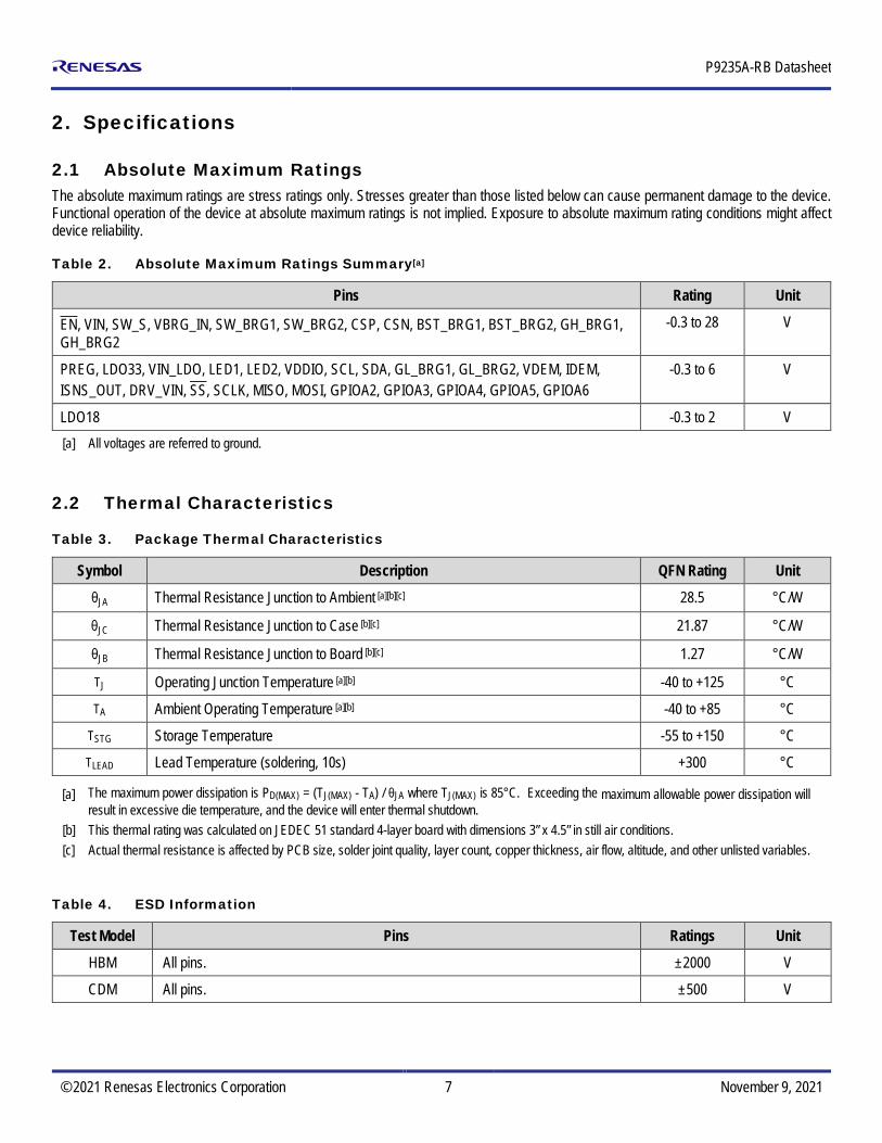
2. Specifications
2.1 Absolute Maximum Ratings The absolute maximum ratings are stress ratings only. Stresses greater than those listed below can cause permanent damage to the device. Functional operation of the device at absolute maximum ratings is not implied. Exposure to absolute maximum rating conditions might affect device reliability.
Table 2. Absolute Maximum Ratings Summary[a]
Pins Rating Unit
EN, VIN, SW_S, VBRG_IN, SW_BRG1, SW_BRG2, CSP, CSN, BST_BRG1, BST_BRG2, GH_BRG1, GH_BRG2
-0.3 to 28 V
PREG, LDO33, VIN_LDO, LED1, LED2, VDDIO, SCL, SDA, GL_BRG1, GL_BRG2, VDEM, IDEM, ISNS_OUT, DRV_VIN, SS, SCLK, MISO, MOSI, GPIOA2, GPIOA3, GPIOA4, GPIOA5, GPIOA6
-0.3 to 6 V
LDO18 -0.3 to 2 V [a] All voltages are referred to ground.
2.2 Thermal Characteristics
Table 3. Package Thermal Characteristics
Symbol Description QFN Rating Unit θJA Thermal Resistance Junction to Ambient [a][b][c] 28.5 °C/W
θJC Thermal Resistance Junction to Case [b][c] 21.87 °C/W
θJB Thermal Resistance Junction to Board [b][c] 1.27 °C/W
TJ Operating Junction Temperature [a][b] -40 to +125 °C TA Ambient Operating Temperature [a][b] -40 to +85 °C
TSTG Storage Temperature -55 to +150 °C TLEAD Lead Temperature (soldering, 10s) +300 °C
[a] The maximum power dissipation is PD(MAX) = (TJ(MAX) - TA) / θJA where TJ(MAX) is 85°C. Exceeding the maximum allowable power dissipation will result in excessive die temperature, and the device will enter thermal shutdown.
[b] This thermal rating was calculated on JEDEC 51 standard 4-layer board with dimensions 3” x 4.5” in still air conditions. [c] Actual thermal resistance is affected by PCB size, solder joint quality, layer count, copper thickness, air flow, altitude, and other unlisted variables.
Table 4. ESD Information
Test Model Pins Ratings Unit HBM All pins. ±2000 V
CDM All pins. ±500 V

P9235A-RB Datasheet
© 2021 Renesas Electronics Corporation 8 November 9, 2021
2.3 Electrical Characteristics
Table 5. Electrical Characteristics
Note: VIN = 5V, EN = LOW, TAMB = -40°C to +85°C, unless otherwise noted. Typical values are at 25°C.
Symbol Description Conditions Minimum Typical Maximum Unit Input Supplies and UVLO VIN Input Operating Range [a] 4.25 21 V
VIN_UVLO Under-Voltage Lockout VIN rising 4.0 V
VIN_UVHYS Under-Voltage Hysteresis VIN falling 0.5 V
IIN Operating Mode Input Current Power-transfer phase, Vin = 12V
10 mA
ISTD_BY Standby Mode Current Periodic ping 1 mA
ISHD Shut-Down Current EN = VIN = 21V 25 80 µA
Enable Pin Threshold (EN)
VIH Input Threshold HIGH 2.5 V
VIL Input Threshold LOW 0.5 V
IEN_LKG EN Pin Input Leakage Current VEN¯¯ = 0V -1 1 µA
VEN¯¯ = 5V 2.5 µA
Step-Down Regulator [b] with COUT = 33µF; L = 4.7µH
VOUT Step-Down Output Voltage Vin = 12V 4.5 5 5.5 V
N-Channel MOSFET Drivers
tLS_ON_OFF Low-Side Gate Driver Rise and Fall Times
CLOAD= 3nF; 10% to 90%, 90% to 10%
50 150 ns
tHS_ON_OFF High-Side Gate Driver Rise and Fall Times
CLOAD = 3nF; 10% to 90%, 90% to 10%
150 300 ns
Input Current Sense
VSEN_OFST Amplifier Output Offset Voltage Measured at the ISNS_OUT pin; VCSP = VCSN
0.6 V
ISENACC_TYP Measured Current Sense Accuracy [c]
VR_ISEN = 25mV, I = 1.25A ±3.5 %
Analog to Digital Converter N Resolution 12 Bit
Channel Number of Channels 10
VIN,FS Full Scale Input Voltage 2.4 V

P9235A-RB Datasheet
© 2021 Renesas Electronics Corporation 9 November 9, 2021
Symbol Description Conditions Minimum Typical Maximum Unit LDO18 [b]
VLDO18 1.8V LDO Regulator COUT = 1µF, VVIN_LDO = 5.5V 1.71 1.8 1.89 V
LDO33 [b] VLDO33 3.3V LDO Regulator COUT = 1µF, VVIN_LDO = 5.5V 3.15 3.3 3.45 V
PREG VPREG 5V LDO Regulator 5 V
Thermal Shutdown
TSD Thermal Shutdown Threshold rising 140 °C
Threshold falling 120 °C
General Purpose Input/Output (GPIO), SS, SCLK, MISO, and MOSI Current Leakage
ILKG Leakage Current -1 1 µA
Output Logic Levels for Open-Drain Pins (LED1, LED2, SCL, SDA)
VOH Output Logic HIGH 4 V
VOL Output Logic LOW I = 8mA 0.5 V
General Purpose Input/Output (GPIO), SS, SCLK, MISO, and MOSI Logic Levels
VIH Input Voltage HIGH Level 0.7 × VDDIO V
VIL Input Voltage LOW Level 0.3 × VDDIO V
ILKG Leakage Current 1 µA
VOH Output Logic HIGH I = 8mA, VDDIO = 3.3V 2.4 V
VOL Output Logic LOW I = 8mA, VDDIO = 3.3V 0.5 V
I2C Interface (SCL, SDA) fSCL_SLV Clock Frequency As I2C slave 400 kHz
CB Capacitive Load For each bus line 100 pF
CBIN SCL, SDA Input Capacitance 5 pF
ILKG Input Leakage Current V = GND and 3.3V -1 1 µA
[a] The input voltage operating range is dependent upon the type of transmitter power stage (full-bridge, half-bridge) and transmitting coil inductance. WPC specifications should be consulted for appropriate input voltage ranges by end-product type.
[b] Do not externally load. For internal biasing only. [c] A 20mΩ, 1% or better sense resistor and a 4.7Ω, 1% input filter resistor are required to meet the FOD specification.

P9235A-RB Datasheet
© 2021 Renesas Electronics Corporation 10 November 9, 2021
3. Typical Performance Characteristics
Figure 2. P9235A-RB TX with 5V Input Supply and P9225-R RX Total System Efficiency Characteristics
Figure 3. P9235A-RB TX and P9225-R RX Startup Waveform into 1.2A Load Current (IOUT) with 5V Input & 1.2A Load Current (IOUT)
30
35
40
45
50
55
60
65
70
75
80
85
90
0 0.2 0.4 0.6 0.8 1 1.2
Effic
ienc
y(%
)
VOUT Current(A)
Total System Efficiency P9235A-RB TX vs. RX P9225-R IOUT(A)

P9235A-RB Datasheet
© 2021 Renesas Electronics Corporation 11 November 9, 2021
4. Block Diagram
EN
BST_BRG2
Half B
ridge
Drive
rs Co
ntrol
32-Bit ARMProcessor
SCLSDA
BST_BRG1
GH_BRG1
SW_BRG1
GL_BRG1
Half B
ridge
Drive
rs Co
ntrol
GH_BRG2
SW_BRG2
GL_BRG2PW
M Ge
nera
toran
d FSK
Mod
ulator
CSN
CSP
+-
+-
ISNS
_OUT
ASKDecoder VBRG_IN
DRV_VIN
ISNS
DATAOTP
DATASRAM
I2C
VIN
5V Buck
LDO33
PREG
LDO18
LDO5VSW_S
VIN_LDO
LDO33
LDO18
5V
3.3V
1.8V
GND
GPIOA2GPIOA3
OSC
GPIOA4GPIOA5GPIOA6
GND
12
MUX
EP
VDDIO
I/OModule
ISNS
VIN
ADC
SCLKSS
MOSIMISO
VDEM
IDEM
I
LED1LED2

P9235A-RB Datasheet
© 2021 Renesas Electronics Corporation 12 November 9, 2021
5. Theory of Operation A wireless power charging system has a base station with one or more transmitters that make power available via DC-to-AC inverter(s) and transmit the power over a strongly-coupled inductor pair to a receiver in a mobile device. The amount of power transferred to the mobile device is controlled by the wireless power receiver by sending communication packets to the transmitter to increase, decrease, or maintain the power level. The communication from receiver to transmitter is purely digital and consists of logic 1’s and 0’s that ride on top of the power link that exists between the transmitter (TX) and receiver (RX) coil. Communication from transmitter to receiver is achieved by frequency shift keying (FSK) modulation over the power signal frequency, and amplitude shift keying (ASK) is used for the communication protocol from receiver to transmitter. A feature of the wireless charging system is the fact that when it is not delivering power, the transmitter is in Standby Mode. The transmitter remains in Standby Mode and periodically pings until it detects the presence of a receiver. Once a Baseline Power Profile (BPP) receiver is detected, such as the P9222-R, P9225-R, or equivalent, the transmitter will provide up to 5W of output power. The P9235A-RB contains features that ensure a high level of functionality and compliance with the WPC requirements, such as a power path that efficiently achieves power transfer, a simple and robust communication demodulation circuit, safety and protection circuits, configuration, and status indication circuits.
5.1 Foreign Object Detection When metallic objects, such as coins, keys, and paperclips, are exposed to alternating magnetic fields, the eddy current flowing through the object will heat it. The amount of heat generated is a function of the amplitude and frequency of the magnetic field, as well as the characteristics of the object, such as resistivity, size, and shape. In any wireless power system, the heat generated by the eddy current manifests itself as a power loss, reducing the overall system efficiency. If appropriate measures are not taken, the heating could lead to unsafe situations. The foreign object detection is performed during power transfer where the power-loss difference between the received power and transmitted power is constantly measured and compared to the WPC-specified threshold. If the difference is higher than the threshold set by the WPC specification, the P9235A-RB will identify it as an FOD and the system will shut down to avoid over-heating.
5.2 Input Voltage The P9235A-RB can support an input voltage from 4.5 to 21V. Depending on the reference design and the WPC coil configuration selection, the input voltage will be limited to a range of operating voltages defined by the WPC specification.
5.3 General Purpose Input/Output – GPIO Pins The P9235A-RB has 5 GPIOs, which can be repurposed in the firmware to do specific functions, such as setting the current limit or FOD limits, driving the additional coils, or sounding a buzzer.
5.4 Enable Pin The P9235A-RB can be disabled by applying a logic HIGH to the EN pin. When the voltage on the EN pin is pulled HIGH, operation is suspended and the P9235A-RB is placed in the low-current Shut-Down Mode. If pulled LOW, the P9235A-RB is enabled and active.

P9235A-RB Datasheet
© 2021 Renesas Electronics Corporation 13 November 9, 2021
5.5 Voltage Demodulation – VDEM In order to increase the communication reliability in any load condition, the P9235A-RB has integrated two demodulation schemes, one based on coil current information and the other based on coil voltage modulation. The voltage mode envelope detector is implemented using a discrete solution as depicted on Figure 4. This simple implementation achieves the envelope detector function low-pass filter as well as the DC filter function.
Figure 4. Voltage Mode Envelope Detector
Coil Voltage(VCOIL)
D1 R14
R11 C19
R13 C22
C17
PacketDecoder
ToRegisters
P9235A-RB
VDEMASK Decoder
5.6 Current Demodulation – IDEM Pin The current-mode detector takes the modulation information from the current sense resistor, which carries the coil current modulation information in addition to the averaged input current. An external discrete low-pass filter and DC filter between the ISNS_OUT and IDEM pins provide additional filtering. The packet decoder block is shared between the voltage-mode and current-mode detectors. The packet decoder selects either voltage-mode or current-mode signals depending upon which produces the best demodulated signal.
Figure 5. Current Mode Envelope Detector
CSP
CSN
VIN Vbridge
ISNS
_OUT
IDEM
PacketDecoder
ToRegisters
20mΩ
R18
P9235A-RB
R6
C9
C8
C7
ASK Decoder
5.7 External Memory The P9235A-RB requires an external flash memory in which firmware must be programmed. Control firmware is programmed into the external flash memory to set operation, control, and FOD parameters. The master P9235A-RB accesses the slave external memory using a standard SPI interface (SCLK, MISO, MOSI, and SS pins) to upload the firmware from the flash memory into the P9235A-RB internal SRAM. The W25X20CLUXIG is the recommended external flash memory. Smaller memory sizes can be used depending on the total firmware size.

P9235A-RB Datasheet
© 2021 Renesas Electronics Corporation 14 November 9, 2021
5.8 Thermal Protection The P9235A-RB integrates thermal shutdown circuitry to prevent damage resulting from excessive thermal stress that might be encountered under fault conditions. This circuitry will shut down or reset the P9235A-RB if the die temperature exceeds a threshold to prevent damage resulting from excessive thermal stress that might be encountered under fault conditions. An internal temperature protection block is enabled in the P9235A-RB that monitors the temperature inside the chip. If the die temperature exceeds 140°C, the P9235A-RB shuts down and resumes when the internal temperature drops below 120°C.
5.9 Integrated Step-Down Regulator The input capacitors must be connected as close as possible between the VIN pin and GND pin. Similarly, the output capacitors must be placed close to the inductor and GND. The output voltage is sensed by the VIN_LDO pin; therefore, the connection from the step-down output (VCC_5V) to the VIN_LDO pin should be made as wide and short as possible to minimize output voltage errors. The step-down regulator is the input voltage to the LDO18 and LDO33 linear regulators and is not recommended for powering an external load.
5.10 Linear Regulators – PREG, LDO33, and LDO18 Pins The P9235A-RB has three low-dropout (LDO) regulators used to bias the internal circuitry. The 5V pre-regulator (PREG) provides bias for the entire internal power management. The PREG requires a 1μF ceramic bypass capacitor connected from the PREG pin to GND. This capacitor must be placed very close to the PREG pin. The voltage regulator must not be externally loaded. The LDO33 and LDO18 are used to bias the internal digital circuit. The regulator’s input voltage is supplied through the VIN_LDO pin. Both regulators require a 1μF ceramic capacitor from the pin to GND. The voltage regulators must not be externally loaded.
5.11 Under-Voltage Lock-Out (UVLO) Protection The P9235A-RB has a 4V (typical, rising) under-voltage lockout circuit on the VIN pin. To guarantee proper functionality, the voltage on the VIN pin must rise above the UVLO threshold. If the input voltage stays below the UVLO threshold, the P9235A-RB is in Shut-Down Mode.
Figure 6. UVLO Threshold Definition
Shut-Down Mode
Shut-Down Mode
Normal Operating Mode
Time
VIN_UVHYS
VIN_UVLO
VIN[
V]

P9235A-RB Datasheet
© 2021 Renesas Electronics Corporation 15 November 9, 2021
5.12 LC Resonant Circuit The LC resonant circuit comprises the series primary resonant coil (LP) and series capacitance (CP) in the application circuit on page 1. The transmitter coil assembly is vendor specific, and it must comply with the WPC recommendation. The WPC specifications include the self-inductance value, DC resistance (DCR), Q-factor, size, and number of turns. The P9235A-RB is designed to support various Baseline Power Profile (BPP) coil configurations using half-bridge and full-bridge inverter topologies to drive the primary coil (LP) and a series capacitance (CP). Depending on the WPC coil configuration selection, the coil inductance and series capacitance will change. Near resonance, the voltage developed across the CP series capacitance could reach 70V peak (voltage will change depending on the coil configuration). High-voltage COG-type ceramic capacitors are highly recommended for their AC and DC characteristics and temperature stability. Film-type capacitors can also be used as recommended by Renesas.
6. Communication Interface
6.1 Modulation/Communication The WPC specification uses two-way communication for power transfer: receiver-to-transmitter and transmitter-to receiver. Receiver-to-transmitter communication is accomplished by the receiver modulating the load seen by the receiver's coil; the communication is purely digital and logic 1’s and 0’s carried on the power signal. Modulation is done with amplitude-shift keying (ASK) modulation using with a bit-rate of 2Kbps. To the P9235A-RB transmitter, this appears as an impedance change, which results in measurable variations of the transmitter’s coil. The P9235A-RB power transmitter demodulates this variation of the coil current or voltage to receive the packets. Transmitter-to-receiver communication is accomplished by frequency-shift keying (FSK) modulation over the power signal frequency. The P9235A-RB power transmitter has the capability to modulate FSK data from the power signal frequency and use it in order to establish the handshaking protocol with the power receiver. The P9235A-RB implements FSK communication when used in conjunction with WPC-compliant receivers, such as the Renesas P9222-R. The FSK communication protocol allows the transmitter to send data to the receiver using the power transfer link in the form of modulating the power transfer signal. This modulation appears in the form of a change in the base operating frequency (fOP) to the modulated operating frequency (fMOD) in periods of 256 consecutive cycles. Equation 1 is used to compute the modulated frequency based on any given operating frequency. Communication packets are transmitted from transmitter to receiver with less than 1% positive frequency deviation following any receiver-to-transmitter communication packet. The frequency deviation is calculated using Equation 1.
fMOD = 60000
60000fOP
− 3 [kHz] Equation 1
Where fMOD is the change in frequency in the power signal frequency; fOP is the base operating frequency of power transfer; and 60000kHz is the frequency of the internal oscillator responsible for counting the period of the power transfer signal. The FSK byte-encoding scheme and packet structure complies with the WPC specification. The FSK communication uses a bi-phase encoding scheme to modulate data bits into the power transfer signal. The start bit will consist of 512 consecutive fMOD cycles (or logic ‘0’). A logic ‘1’ value will be sent by sending 256 consecutive fOP cycles followed by 256 fMOD cycles or vice versa, and a logic ‘0’ is sent by sending 512 consecutive fMOD or fOP cycles.

P9235A-RB Datasheet
© 2021 Renesas Electronics Corporation 16 November 9, 2021
Figure 7. Example of Differential Bi-phase Encoding for FSK
tCLK = 256/fOP
ONE ZERO ONE ZERO ONE ONE ZERO ZERO
512 cycles 256 cycles
Each byte will comply with the start, data, parity, and stop asynchronous serial format structure shown in Figure 8:
Figure 8. Example of Asynchronous Serial Byte Format for FSK
Start StopParityb0 1 2 3 4 5 6 7b b b b b b b
6.2 Bit Decoding Scheme for ASK As required by the WPC, the P9235A-RB uses a differential bi-phase coding scheme to demodulate data bits onto the power signal. A clock frequency of 2kHz is used for this purpose. A logic ONE bit is coded using two narrow transitions, whereas a logic ZERO bit is encoded using one wider transition as shown in Figure 9:
Figure 9. Bit Decoding Scheme
t CLK
ONE ZERO ONE ZERO ONE ONE ZERO ZERO
6.3 Byte Decoding for ASK Each byte in the communication packet comprises 11 bits in an asynchronous serial format, as shown in Figure 10.
Figure 10. Byte Decoding Scheme
Start StopParityb0 1 2 3 4 5 6 7b b b b b b b
Each byte has a start bit, 8 data bits, a parity bit, and a single stop bit.

P9235A-RB Datasheet
© 2021 Renesas Electronics Corporation 17 November 9, 2021
6.4 Packet Structure The P9235A-RB communicates with the base station via communication packets. Each communication packet has the following structure:
Figure 11. Communication Packet Structure
Preamble Header Message Checksum
7. Bi-Directional User Data Communication Note: Only application firmware version 2.17, and higher, will allow Bi-Directional User Data Communication. To download the latest firmware update, visit the P9235A-RB-EVK reference design page. In customer-end systems, the transmitter and receiver boards must have an external microcontroller (MCU) or leverage an existing on-board application processor to orchestrate bi-directional communication. Using the I2C communication, the MCU on the transmitter board loads the user data into specific registers and triggers the communication. The P9235A-RB sends the data to the P9222-R using frequency shift keying (FSK) modulation. The P9222-R then receives the data and interrupts the MCU on the receiver when the data is ready to be read. The external MCU on the receiver follows the same procedure to send the data to the P9235A-RB using amplitude-shift keying (ASK) modulation. When new data is available to read, the P9235A-RB interrupts the external MCU on the transmitter board. Bi-directional user data communication is enabled only in the power transfer phase. The external MCU on the transmitter board can read the State register to determine whether the P9235A-RB is in the power transfer phase.
7.1 Transferring Data from the P9235A-RB to the P9222-R The external MCU on the transmitter board should determine the status of the communication channel before initiating a new transfer. The P9235A-RB provides SRAM registers of outgoing user data registers, header register, and communication trigger register (or command register). The external MCU on the transmitter should set communication trigger register after loading the appropriate user data into the header register and outgoing user data register. The P9235A-RB waits until it receives the Control Error Packet (CEP) from the P9222-R, as the receiver device has the master role within the communication process. Afterwards, the P9235A-RB sends the data into the channel by FSK (Frequency Shift Key) modulation. Error! Reference source not found. shows the timing diagram for the user data transfer from the P9235A-RB to the P9222-R.
Figure 12. Timing Diagram for the User Data Transfer from the P9235A-RB to the P9222-R
7.2 Reading Data Sent from the P9222-R When the P9235A-RB receives data from the P9222-R, the P9235A-RB will generate an interrupt to the external MCU on the transmitter by pulling down the interrupt pin. The MCU can respond to the interrupt and read the received data. After reading the data, the external MCU on the transmitter should clear the interrupt. If the external MCU on the transmitter does not handle interrupts, the MCU should constantly poll the data received flag to check whether there is any new incoming data. If the external MCU on the transmitter does not read data immediately after the interrupt is received, there is a risk that data could become corrupted/overwritten because of next new incoming data. The user can implement a higher-level handshaking protocol between the external MCU on transmitter and receiver to avoid data corruption.

P9235A-RB Datasheet
© 2021 Renesas Electronics Corporation 18 November 9, 2021
8. I2C Interface The P9235A-RB supports the standard I2C interface. The default I2C slave address is 0x61. Figure 13 shows the Read and Write protocol structure that the external I2C master must use to communicate with the P9235A-RB.
Figure 13. I2C Access Read Protocol and Write Protocol
From Master
From Slave
ACK ACK ACK
DataByte_1 A A DataByte_3 A
8 1 8 1 8 1
ACK
DataByte_0 A
8 1Clocks
. . . .DataByte_2
Start 61HEX 61HEXACK 06HEX ACK 80HEX ACK ACKR/W R/W
S Slave Address Sr Slave AddressA Memory AddressMSB0 A Memory Address
LSB A 1 A . . . .1 7 71 8 1 8 1 11 1Clocks
Read Protocol
P
ACK ACK
CmdByte_1 A A CmdFlag_1
8 1 8 1 8 1
ACK
CmdByte_0 A
8 1Clocks
CmdFlag_0 A/A
1
NAK
LSB = Least Significant ByteMSB = Most Significant Byte
A = Acknowledge (SDA LOW)A = Not Acknowledge (SDA HIGH)S = Start ConditionSr = Restart ConditionP = Stop Condition
From Master
From Slave
ACK ACK ACK
DataByte_1 A A DataByte_3 A
8 1 8 1 8 1
ACK
DataByte_0 A
8 1Clocks
. . . .DataByte_2
Write Protocol
P
ACK ACK
CmdByte_1 A A CmdFlag_1
8 1 8 1 8 1
ACK
CmdByte_0 A
8 1Clocks
CmdFlag_0 A/A
1
NAK
Start 61HEX ACK 06HEX ACK 80HEX ACKR/W
S Slave Address A Memory AddressMSB0 A Memory Address
LSB A . . . .1 7 1 8 1 8 11Clocks
LSB = Least Significant ByteMSB = Most Significant Byte
A = Acknowledge (SDA LOW)A = Not Acknowledge (SDA HIGH)S = Start ConditionSr = Restart ConditionP = Stop Condition

P9235A-RB Datasheet
© 2021 Renesas Electronics Corporation 19 November 9, 2021
9. Application Information
9.1 Power Dissipation and Thermal Requirements The P9235A-RB is offered in a 40-VFQFPN package that has a maximum power dissipation capability of approximately 1.2W. The number of thermal vias between the package and the printed circuit board determines the maximum power dissipation. The maximum power dissipation of the package is limited by the die’s specified maximum operating junction temperature, TJ(MAX), of 125°C, the maximum ambient operating temperature, TA, of 85°C, and the package thermal resistance, θJA. The junction temperature rises when the heat generated by the device’s power dissipation flows through the package thermal resistance. The VFQFPN package offers a typical thermal resistance, junction to ambient (θJA), of 28.5°C/W when the PCB layout guideline and surrounding devices are optimized. The techniques as noted in the PCB layout section of the P9235A-RB EVK User Manual (available on the P9235A-RB-EVK product page) must be followed when designing the printed circuit board layout. Take into consideration possible proximity to other heat-generating devices when placing the P9235A-RB and the bridge FET packages in a given application design. The ambient temperature around the power IC will also have an effect on the thermal limits of an application. The main factors influencing θJA (in the order of decreasing influence) are PCB characteristics, the size of the thermal pad attached to the die/package (VFQFPN), the thermal vias, and final system hardware construction. Board designers should keep in mind that the package thermal metric θJA is impacted by the characteristics of the PCB. Changing the design or configuration of the PCB changes the overall thermal resistivity and the board’s heat-sinking efficiency. The use of integrated circuits in low-profile and fine-pitch surface-mount packages requires special attention to power dissipation. Many system-dependent issues, such as thermal coupling, airflow, added heat sinks, convection surfaces, and the presence of other heat-generating components, affect the power-dissipation limits of a given component. In summary, the three basic approaches for enhancing thermal performance include: Improving the power dissipation capability of the PCB design Improving the thermal coupling of the component to the PCB Introducing airflow into the system The maximum power dissipation for a given situation should be calculated using Equation 2:
PD(MAX) =TJ(MAX) – TA
θJA
Equation 2
Where: PD(MAX) = Maximum Power Dissipation θJA = Package Thermal Resistance (°C/W) TJ(MAX) = Maximum Device Junction Temperature (°C) TA = Ambient Temperature (°C)
The maximum recommended operating junction temperature (TJ(MAX)) for the P9235A-RB device is 120°C. The thermal resistance of the 40-VFQFPN package is optimally θJA = 28.5°C/W. Operation is specified to a maximum steady-state ambient temperature (TA) of 85°C. Therefore, the maximum recommended power dissipation is calculated with Equation 3.
PD(MAX) =(120°C – 85°C)
28.5°C/W ≅ 1.2W Equation 3
All the previously mentioned thermal resistances are the values found when the P9235A-RB is mounted on a standard board of the dimensions and characteristics specified by the JEDEC 51 standard. To allow the maximum load current and to prevent thermal overload, the heat generated by the P9235A-RB solution must be dissipated into the PCB. All the available pins must be soldered to the PCB. GND pins (exposed paddle, EP) and bridge FET GND pins should be soldered to the PCB ground plane to improve thermal performance, with multiple vias connected to all layers of the PCB.

P9235A-RB Datasheet
© 2021 Renesas Electronics Corporation 20 November 9, 2021
9.2 P9235A-RB Evaluation Board v1.1 Schematic Note: The typical application schematic provides a basic guideline to understanding and building a functional small-power wireless power transmitter type as described in the WPC specifications. Other components not shown on the typical application schematic may be needed in order to comply with other requirements, such as EMC or thermal specifications.
Figure 14. P9235A-RB Typical Application Schematic
SCL
SCLK
R72
10k
0402
LED_
PATT
/FOD
_ADJ
THIS
DOC
UMEN
T CO
NTAI
NS I
NFOR
MATI
ON P
ROPR
IETA
RYTO
Ren
esas
Ele
ctro
nics
Ame
rica
, IN
C. (
REA)
.US
E OR
DIS
CLOS
URE
WITH
OUT
THE
WRIT
TEN
PERM
ISSI
ON O
F AN
OFF
ICER
OF
REA
IS
EXPR
ESSL
Y FO
RBID
DEN
R31
NP
R40
22 0402
R2 0 1206
L5 INDU
CTOR
VBRI
DGE
C24
NP 10V
0603
IDEM
VIN_
1
VSNS
_IN1
LDO3
3
C70
5.6nF
25V
0603
R47
22 0402
C76
NP
VDEM
1
CSP
R70
47K
0402
VIN_
SEL
FOD_ADJ
NOTE 1 - FOD_ADJ (GPIOA2) function is removed. Do not populate.
Use REA PRO GUI to change defaults.
NOTE 2 - LED_PATT (GPIOA3) function is removed. Do not populate.
Use REA PRO GUI to change defaults.
C20
680p
F10
V04
02
LDO1
8
C18
22nF
25V
0402
GPIO
A6
R27
NP
LED2
D2 BAV2
1WS
SOD-
323
VCC_
5V
LED1
21
C30
0.1uF
10V
0402
LDO3
3
R26
0.02
0805
C43
1uF
10V
0603
D3
NP
C7 10uF
10V
0603
SW_B
RG2
BRG1
_HG
VIN_
SNS
GND_
SNS
TS
U7
W25
X40C
LUXIG
CS#
1
DO2
WP#
3
GND
4DI
5CL
K6
HLD#
7VC
C8
EPAD9
TS
SDA
SW_B
RG1
Q7
AM79
30N
2
34
65 1
SW_B
RG1
GND4
MISO
R23
200K
0402
C3 NP 10V
0402
R9 0 1206
R59N
P
VIN
MISO
LX2
C8 0.1uF
10V
0402
GND1
LDO33
C56
10uF
10V
0603
R35
22 0402
C37
1uF
10V
0603
VIN
SW_B
RG1
Vcoil
R52
5.1k
0402
C44
100n
F50
V12
06
LDO3
3
NOTE 1
NOTE 2
Vsns
C66
0.1uF
10V
0402
LDO3
3
SCLK
R57
100K
0402
GND2
_TP
C27
NP 25V
0603
PLACE FLASH NEXT TO P923x
R60
10k
0402
SCL
ONLY
USE
C0G
CAP
S
C69
22nF
16V
0402
VCC_
5VSW
_BRG
2
C26
NP 25V
0603
R77N
P
C29
680p
F10
V04
02
OPTI
ONAL
FOD_
ADJ
VCC5
V
USB-
MICR
O CO
NNEC
TOR
R76
10k
0402
VCC_
5V
Vsns
GND
C81
NP 10V
0603
LED_PATT
R25
10 0402
C35
10uF
10V
0603
R36
100K
0402
SW_B
RG2
BRG2
_HG
SCL
R22
10 0402
VIN
LED_
PATT
C34
0.1uF
10V
0402
C51
NP
MOSI
GND_
SEL
SDA
C21
22nF
16V
0402
C42
10uF
10V
0603
C46
0.1uF
10V
0402
C47
100n
F50
V12
06
FOD_
ADJ
C67
0.1uF
10V
0402
C19
5.6nF
25V
0603
SDA
MOSI
P923
5A-R
B
U3 EN1
GND
2
PREG
3
VIN
4
SW_S
5
GND1
6
LDO3
37
VIN_
LDO
8
LDO1
89
LED1
10
LED211
VDDIO12
SS20
SCLK
21
MISO
22
MOSI
23
GH_B
RG2
24
BST_
BRG2
25
SW_B
RG2
26
GL_B
RG2
27
GND2
28
GL_B
RG1
29
SW_B
RG1
30
EP41
BST_ BRG131
GH_BRG132
DRV_VIN33
VBRG_IN34
GND335
VDEM136
IDEMI37
ISNS_OUT38
CSN39
CSP40
SCL13
SDA14
GPIOA215
GPIOA316
GPIOA417
GPIOA518
GPIOA619
SS
CSP
MISO
RED
tTH_C
oil1
0603
10K
R34
NP
GND2
C45
10uF
10V
0603
SCLK
SS
D-
CSN
CSN
R43
1K 0402
R61
10k
0402
D+
C48
100n
F50
V12
06
VIN_
SEL
SLD
SLDVC
CD-D+IDGND
J11
usb_
micro
_ab12345
67 89 1011
LED2
21
R44
22 0402
TS
MOSI
Vcoil
COIL
TEM
PERA
TURE
SEN
SING
BRG2
_LG
FLAS
H RE
QUIR
ED
C32
10uF
10V
0603
R45
100K
0402
Title
Size
Docu
ment
Numb
erRe
v
Date:
Shee
tof
1.1
P923
5A-R
B-DE
MO B
RD V
1.1
Custo
m
11
Wed
nesd
ay, A
pril 2
2, 20
20
R48
100K
0402
LDO3
3
LDO3
3PLACE THERMISTOR NEAR COIL ASSEMBLY
GND4
_TP
C50
1uF
6.3V
0603
C68
0.1uF
10V
0402
L1NP
123 4
BRG1
_LG
C77
NP
R20
2.4K
0603
R62N
P
C28
56pF
50V
0402
C38
0.1uF
10V
0402
C55
10uF
10V
0603
R50
5.1k
0402
R30
NP
C2 NP 10V
0603
R42
100K
0402
GPIO
A6
VDEM1
R39
0 0402
C59
47nF
16V
0603
R49
0 0402
CSN
C57
0.1uF
10V
0402
C53
1uF
6.3V
0603
LDO1
8
SW_B
RG2
J4
Prog
Con
n
11
22
33
44
55
R41
1K 0402
LDO3
3
Vcoil
C39
47nF
16V
0603
LDO3
3
LDO3
3
SDA
C49
100n
F50
V12
06
C33
0.1uF
10V
0402
EN
C31
10uF
10V
0603
GREEN
R46
680
0402
R16
NP
R58
10k
0402
R28
10k
0402
LX1
SW_B
RG1
R29 NP
CSP
GND3
LED1
LED_
PATT
C36
NP
Q5
AM79
30N
2
34
65 1
SCL
L4 4.7uH
0603
VBRI
DGE
P9235A-RB DEVELOPMENT BOARD V1.1

P9235A-RB Datasheet
© 2021 Renesas Electronics Corporation 21 November 9, 2021
10. Package Outline Drawings The package outline drawings are located at the end of this document and are accessible from the Renesas website (see package links in Ordering Information). The package information is the most current data available and is subject to change without revision of this document.
11. QFN Package Assembly Unopened dry packaged parts have a one-year shelf life. The HIC indicator card for newly opened dry packaged parts should be checked. If there is any moisture content, the parts must be baked for a minimum of 8 hours at 125˚C within 24 hours prior to the assembly reflow process.
12. Marking Diagram
Line 1: Company name and truncated part number. Line 2: 5A-RB is part of the part number indicating a pre-programmed bootloader IC,
which is followed by the package code. Line 3: “YYWW” is the last two digits of the year and two digits for the work week
that the part was assembled. “#” is the device step.“$” denotes the mark code.
13. Ordering Information Part Number Description and Package MSL Rating Carrier Type Temp. Range
P9235A-RBNDGI P9235A-RB Wireless Power Transmitter for 5W Applications with the Programmed Bootloader, 40-VFQFPN, 5 × 5 mm package
MSL1 Tray -40°C to +85°C
P9235A-RBNDGI8 P9235A-RB Wireless Power Transmitter for 5W Applications with the Programmed Bootloader, 40-VFQFPN, 5 × 5 mm package
MSL1 Reel -40°C to +85°C
14. Revision History Revision Date Description of Change
Nov 9, 2021 Added new sections, “Bi-Directional User Data Communication” and “Application Information” Updated the package outline drawings; however, no mechanical changes Completed other minor changes
Mar 8, 2019 Initial release.

Corporate HeadquartersTOYOSU FORESIA, 3-2-24 Toyosu,Koto-ku, Tokyo 135-0061, Japanwww.renesas.com
Contact InformationFor further information on a product, technology, the most up-to-date version of a document, or your nearest sales office, please visit:www.renesas.com/contact/
TrademarksRenesas and the Renesas logo are trademarks of Renesas Electronics Corporation. All trademarks and registered trademarks are the property of their respective owners.
IMPORTANT NOTICE AND DISCLAIMER
RENESAS ELECTRONICS CORPORATION AND ITS SUBSIDIARIES (“RENESAS”) PROVIDES TECHNICAL SPECIFICATIONS AND RELIABILITY DATA (INCLUDING DATASHEETS), DESIGN RESOURCES (INCLUDING REFERENCE DESIGNS), APPLICATION OR OTHER DESIGN ADVICE, WEB TOOLS, SAFETY INFORMATION, AND OTHER RESOURCES “AS IS” AND WITH ALL FAULTS, AND DISCLAIMS ALL WARRANTIES, EXPRESS OR IMPLIED, INCLUDING, WITHOUT LIMITATION, ANY IMPLIED WARRANTIES OF MERCHANTABILITY, FITNESS FOR A PARTICULAR PURPOSE, OR NON-INFRINGEMENT OF THIRD PARTY INTELLECTUAL PROPERTY RIGHTS.
These resources are intended for developers skilled in the art designing with Renesas products. You are solely responsible for (1) selecting the appropriate products for your application, (2) designing, validating, and testing your application, and (3) ensuring your application meets applicable standards, and any other safety, security, or other requirements. These resources are subject to change without notice. Renesas grants you permission to use these resources only for development of an application that uses Renesas products. Other reproduction or use of these resources is strictly prohibited. No license is granted to any other Renesas intellectual property or to any third party intellectual property. Renesas disclaims responsibility for, and you will fully indemnify Renesas and its representatives against, any claims, damages, costs, losses, or liabilities arising out of your use of these resources. Renesas' products are provided only subject to Renesas' Terms and Conditions of Sale or other applicable terms agreed to in writing. No use of any Renesas resources expands or otherwise alters any applicable warranties or warranty disclaimers for these products.
(Rev.1.0 Mar 2020)
© 2020 Renesas Electronics Corporation. All rights reserved.