Embed Size (px)
Citation preview
© 2011 ANSYS, Inc. April 27, 20151
Wireless Power Transfer System Design
Julius Saitz
ANSYS
© 2011 ANSYS, Inc. April 27, 20152
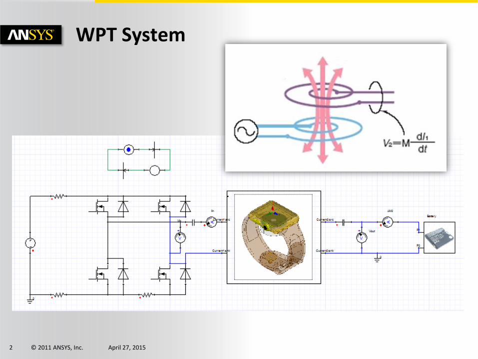
WPT System
© 2011 ANSYS, Inc. April 27, 20153
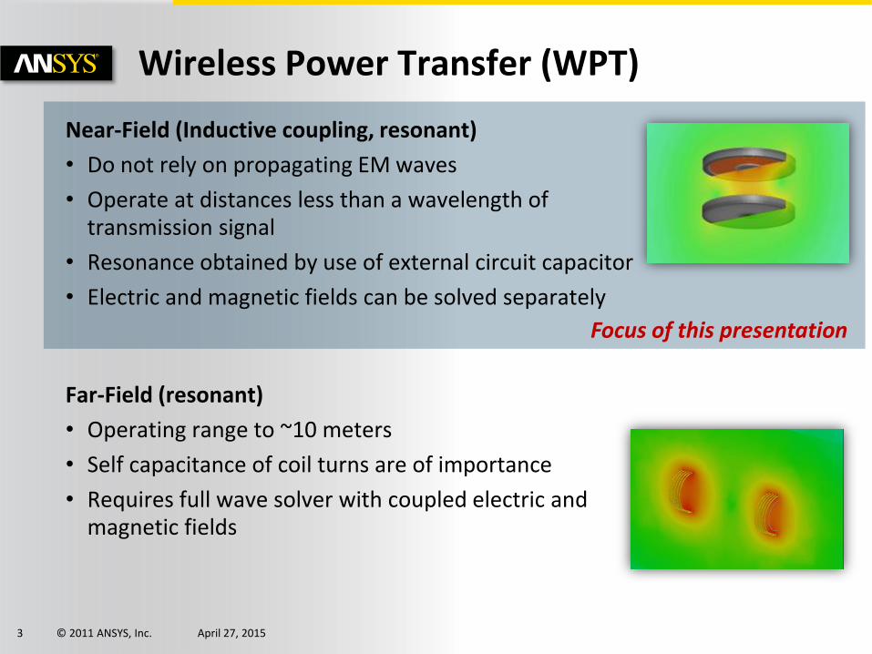
Near-Field (Inductive coupling, resonant)
• Do not rely on propagating EM waves
• Operate at distances less than a wavelength of transmission signal
• Resonance obtained by use of external circuit capacitor
• Electric and magnetic fields can be solved separately
Far-Field (resonant)
• Operating range to ~10 meters
• Self capacitance of coil turns are of importance
• Requires full wave solver with coupled electric and magnetic fields
Wireless Power Transfer (WPT)
Focus of this presentation
© 2011 ANSYS, Inc. April 27, 20154
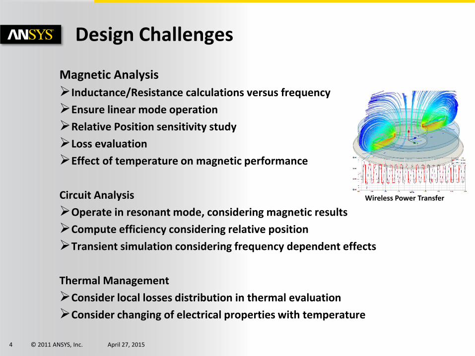
Magnetic Analysis
Inductance/Resistance calculations versus frequency
Ensure linear mode operation
Relative Position sensitivity study
Loss evaluation
Effect of temperature on magnetic performance
Circuit Analysis
Operate in resonant mode, considering magnetic results
Compute efficiency considering relative position
Transient simulation considering frequency dependent effects
Thermal Management
Consider local losses distribution in thermal evaluation
Consider changing of electrical properties with temperature
Design Challenges
Wireless Power Transfer
© 2011 ANSYS, Inc. April 27, 20155
Outline
Large Gap Transformer Design Using Computational Electromagnetics
Combination of Circuit and Magnetic Analysis for Resonance
Thermal Management

© 2011 ANSYS, Inc. April 27, 20156
Large Gap Transformer Design Using Computational Electromagnetics
© 2011 ANSYS, Inc. April 27, 20157
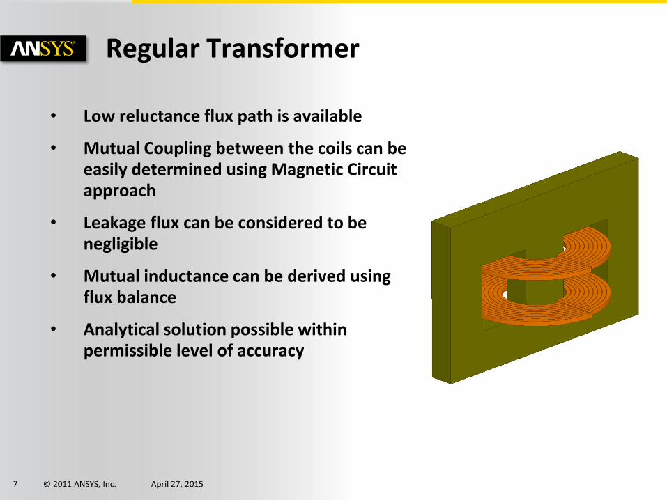
• Low reluctance flux path is available
• Mutual Coupling between the coils can be easily determined using Magnetic Circuit approach
• Leakage flux can be considered to be negligible
• Mutual inductance can be derived using flux balance
• Analytical solution possible within permissible level of accuracy
Regular Transformer
© 2011 ANSYS, Inc. April 27, 20158
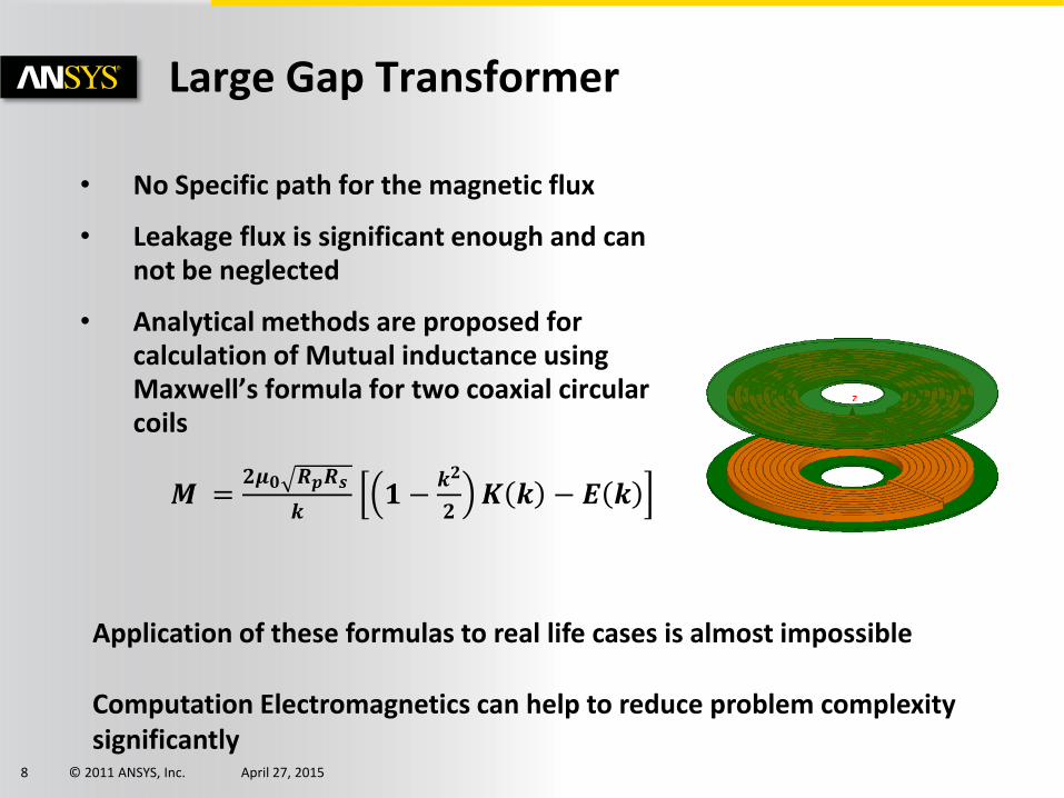
• No Specific path for the magnetic flux
• Leakage flux is significant enough and can not be neglected
• Analytical methods are proposed for calculation of Mutual inductance using Maxwell’s formula for two coaxial circular coils
Large Gap Transformer
𝑴 =𝟐𝝁𝟎 𝑹𝒑𝑹𝒔
𝒌𝟏 −
𝒌𝟐
𝟐𝑲 𝒌 − 𝑬 𝒌
Application of these formulas to real life cases is almost impossible
Computation Electromagnetics can help to reduce problem complexity significantly
© 2011 ANSYS, Inc. April 27, 20159
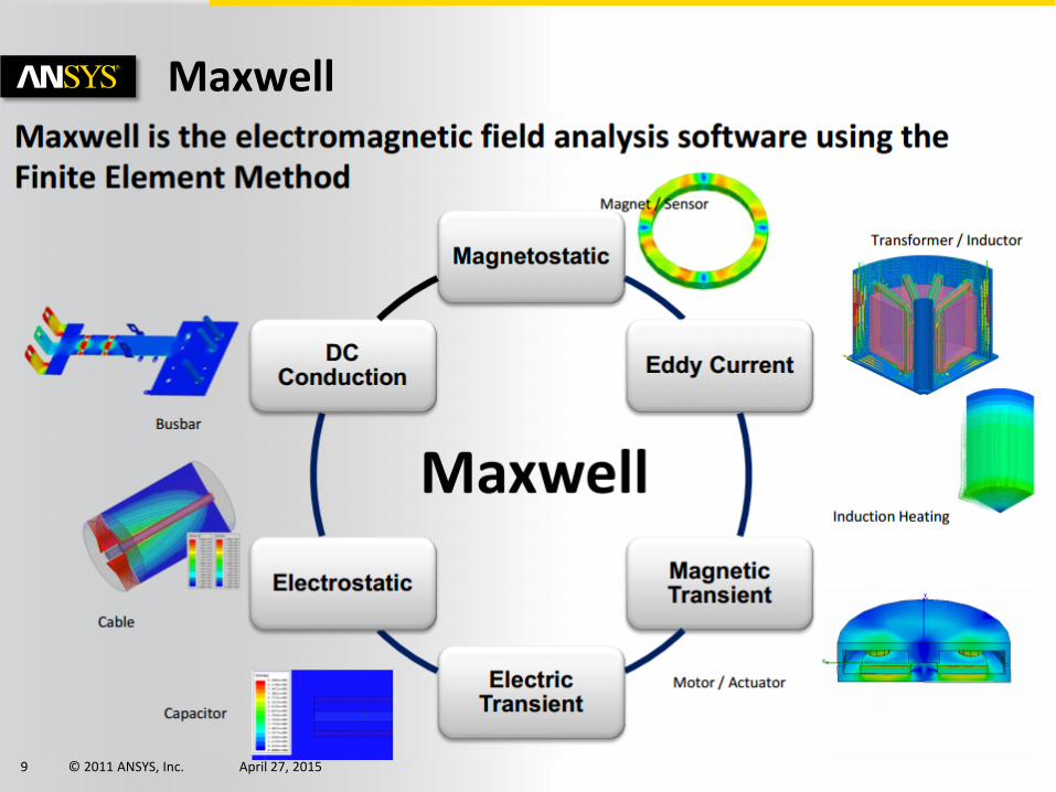
Maxwell
© 2011 ANSYS, Inc. April 27, 201510
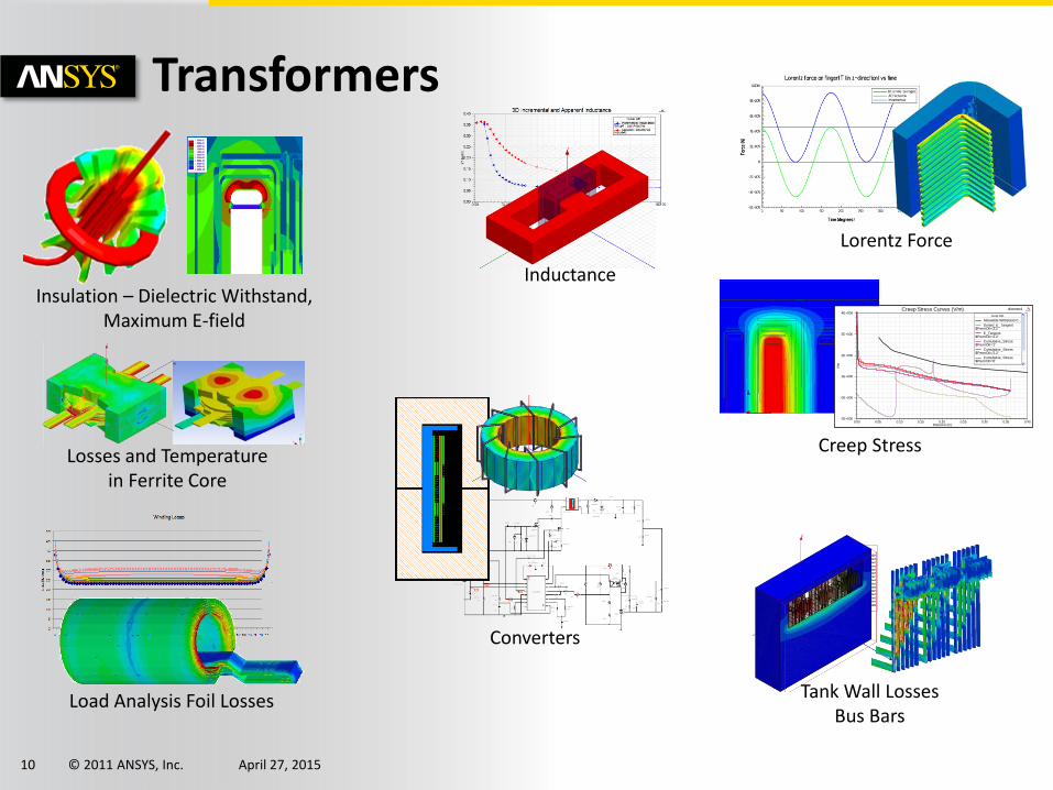
Transformers
Insulation – Dielectric Withstand, Maximum E-field
Load Analysis Foil Losses
Lorentz Force
Tank Wall Losses Bus Bars
Inductance
Losses and Temperature in Ferrite Core
Converters
Creep Stress
0.00 0.05 0.10 0.15 0.20 0.25 0.30 0.35 0.40Distance (m)
-1E+006
0E+000
1E+006
2E+006
3E+006
4E+006
V/m
xformer4Creep Stress Curves (V/m) ANSOFT
Curve Info
Allowable Withstand C...
Sorted_E_Tangent$PermOil='2.2'
E_Tangent$PermOil='2.2'
Cumulative_Stress$PermOil='1'
Cumulative_Stress$PermOil='2.2'
Cumulative_Stress$PermOil='6'
© 2011 ANSYS, Inc. April 27, 201511
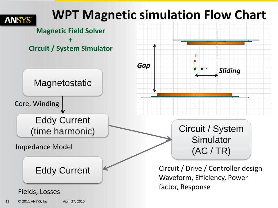
GapSliding
WPT Magnetic simulation Flow ChartMagnetic Field Solver
+ Circuit / System Simulator
Magnetostatic
Eddy Current
(time harmonic) Circuit / System
Simulator
(AC / TR)Impedance Model
Circuit / Drive / Controller designWaveform, Efficiency, Power factor, Response
Eddy Current
Fields, Losses
Core, Winding
© 2012 ANSYS, Inc. April 27, 201512
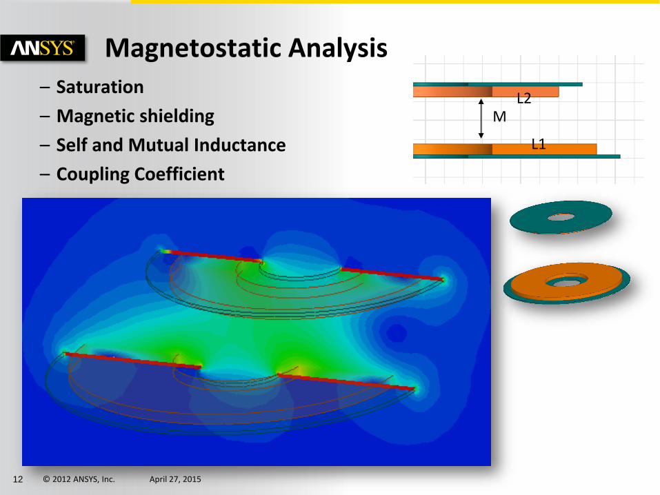
Magnetostatic Analysis– Saturation
– Magnetic shielding
– Self and Mutual Inductance
– Coupling Coefficient
M
L1
L2
© 2011 ANSYS, Inc. April 27, 201513
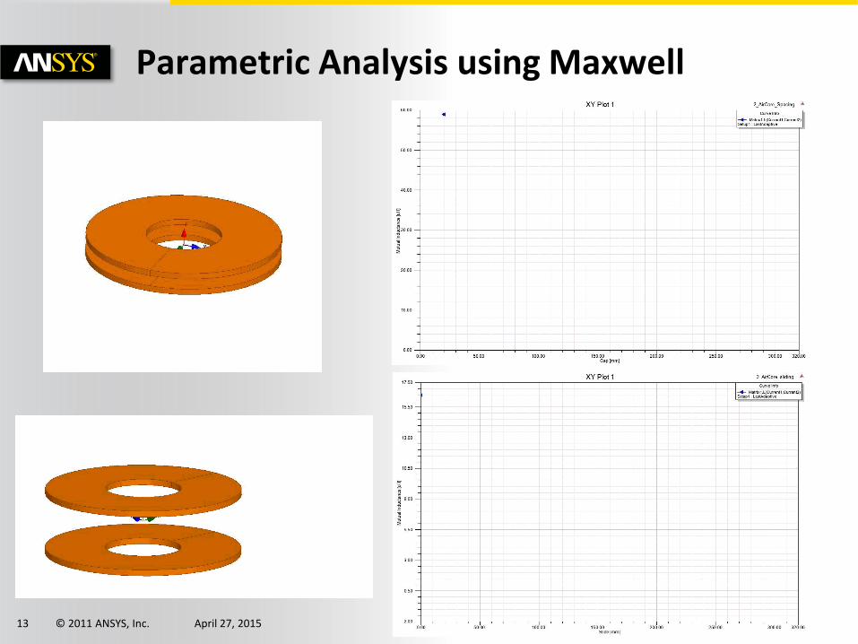
Parametric Analysis using Maxwell
© 2011 ANSYS, Inc. April 27, 201514
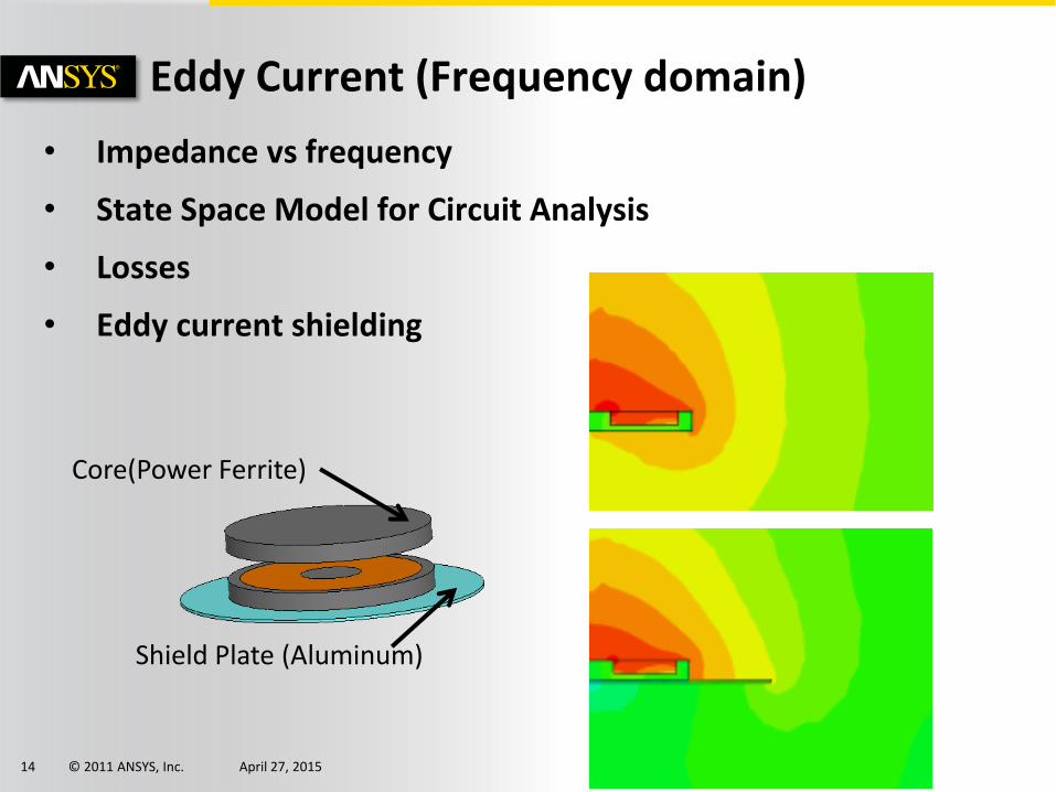
Eddy Current (Frequency domain)
• Impedance vs frequency
• State Space Model for Circuit Analysis
• Losses
• Eddy current shielding
Shield Plate (Aluminum)
Core(Power Ferrite)
© 2011 ANSYS, Inc. April 27, 201515
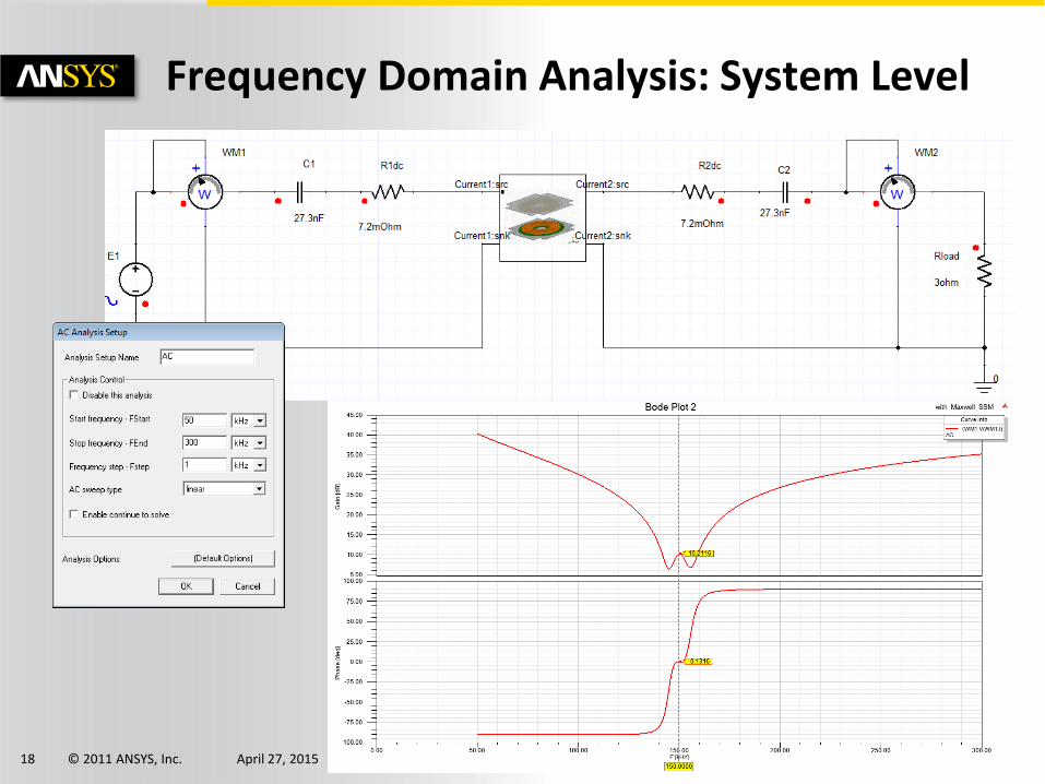
Combination of Circuit and Magnetic Analysis for Resonance
© 2012 ANSYS, Inc. April 27, 201516
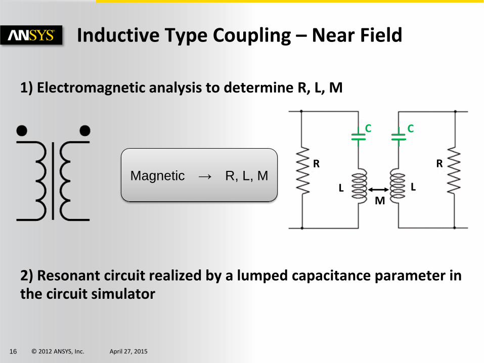
Inductive Type Coupling – Near Field
1) Electromagnetic analysis to determine R, L, M
Magnetic → R, L, MR
C C
R
LLM
2) Resonant circuit realized by a lumped capacitance parameter in the circuit simulator
© 2011 ANSYS, Inc. April 27, 201517
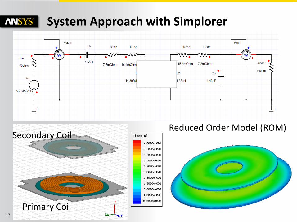
System Approach with Simplorer
Secondary Coil
Primary Coil
Reduced Order Model (ROM)
© 2011 ANSYS, Inc. April 27, 201518
Frequency Domain Analysis: System Level
© 2011 ANSYS, Inc. April 27, 201519
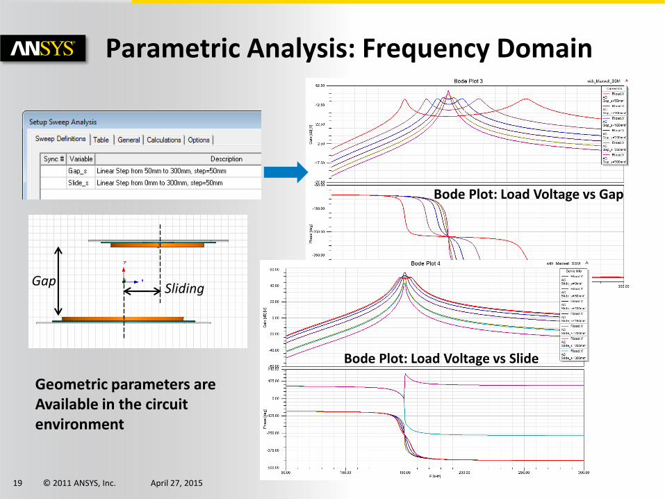
Parametric Analysis: Frequency Domain
Bode Plot: Load Voltage vs Gap
Bode Plot: Load Voltage vs Slide
GapSliding
Geometric parameters areAvailable in the circuit environment
© 2011 ANSYS, Inc. April 27, 201520
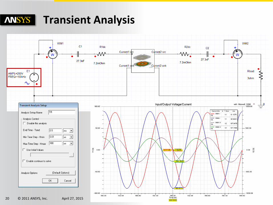
Transient Analysis
© 2011 ANSYS, Inc. April 27, 201521
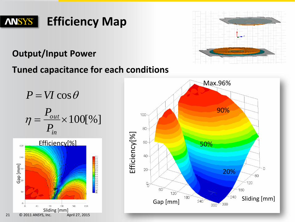
Efficiency Map
Output/Input Power
Tuned capacitance for each conditions
90%
50%
20%
[%]100
cos
in
out
P
P
VIP
Effi
cien
cy[%
]
Sliding [mm]Gap [mm]
Max.96%
Gap
[m
m]
Sliding [mm]
Efficiency[%]
© 2011 ANSYS, Inc. April 27, 201522
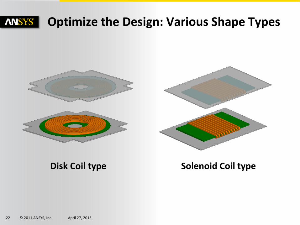
Optimize the Design: Various Shape Types
Disk Coil type Solenoid Coil type
© 2011 ANSYS, Inc.23
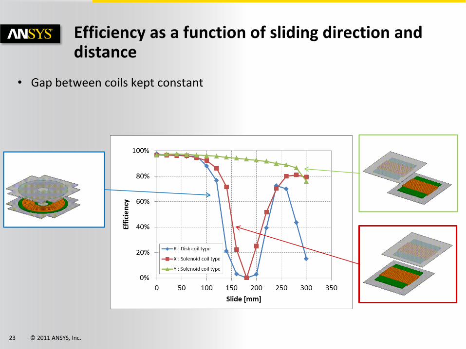
Efficiency as a function of sliding direction and distance
• Gap between coils kept constant
© 2011 ANSYS, Inc.24
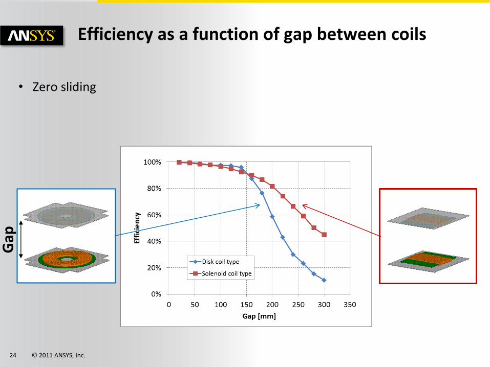
Efficiency as a function of gap between coils
• Zero sliding
Gap
© 2011 ANSYS, Inc. April 27, 201525
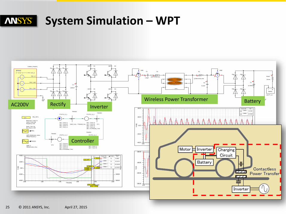
System Simulation – WPT
0
0
0
R1
(1/87-0.004) ohm
R2
(1/348-0.001) ohm
Cs
1.93uF
Cp
5.24uF
Rload
10ohm
W
+
WM1
W
+
WM2
D4
D3
D2
D1
IGBT4
IGBT3
IGBT2
IGBT1
C1
1000uF
TRANS4
DT4
TRANS3
SINE1.VAL > TRIANG1.VAL
TRANS2
DT1
TRANS1
SINE1.VAL < TRIANG1.VAL
STATE_11_4
SET: TSV4:=0SET: TSV3:=0SET: TSV2:=0
SET: TSV1:=0DEL: DT4##Dead_Time
STATE_11_3
SET: TSV4:=0SET: TSV3:=1SET: TSV2:=1
SET: TSV1:=0
STATE_11_2
SET: TSV4:=0
SET: TSV3:=0SET: TSV2:=0
SET: TSV1:=0DEL: DT1##Dead_Time
STATE_11_1
SET: TSV4:=1
SET: TSV3:=0SET: TSV2:=0
SET: TSV1:=1
TRIANG1
AMPL=1FREQ=Carrier_Freq
SINE1
AMPL=Modulation_IndexFREQ=Frequency
ICA:FML_INIT1
Modulation_Index:=0
Carrier_Freq:=10kFrequency:=10k
DC_Source:=200Dead_Time:=2u
~
3PHAS
~
~
A * sin (2 * pi * f * t + PHI + phi_u)
PHI = 0°
PHI = -120°
PHI = -240°
THREE_PHASE1
D5
D6
D7
D8
D9
D10 Battery
- +
LBATT_A1
D11
D12
D13
D14
C2
1e-006farad
0.00 0.25 0.50 0.75 1.00 1.25 1.50 1.75 2.00Time [ms]
-40.00
-20.00
0.00
20.00
40.00
Y1 [A
]
Curve Info rms
WM1.ITR 9.4139
WM2.ITR 10.5939
0.00 0.25 0.50 0.75 1.00 1.25 1.50 1.75 2.00Time [ms]
-300.00
-100.00
100.00
300.00
Y1 [V
]
Curve Info rms
WM1.VTR 154.9045
WM2.VTR 120.2425
1.90 1.92 1.94 1.96 1.98 2.00Time [ms]
-40.00
-20.00
0.00
20.00
40.00
Y1 [A
]
-200.00
-100.00
0.00
100.00
200.00
Y2 [V
]
MX1: 1.9753MX2: 1.9783
-6.0797
-1.2036-0.0090
131.1979
-0.51411.340627.9814
156.0455
0.0030
Curve Info Y Axis rms
WM1.ITR Y1 9.3501
WM2.ITR Y1 10.5176
WM1.VTR Y2 153.6594
WM2.VTR Y2 119.4615
Current_1st_1:src
Current_1st_2:src
Current_2nd_1:src
Current_2nd_2:src
Current_1st_1:snk
Current_1st_2:snk
Current_2nd_1:snk
Current_2nd_2:snk
0
0
0
R1
(1/87-0.004) ohm
R2
(1/348-0.001) ohm
Cs
1.93uF
Cp
5.24uF
Rload
10ohm
W
+
WM1
W
+
WM2
D4
D3
D2
D1
IGBT4
IGBT3
IGBT2
IGBT1
C1
1000uF
TRANS4
DT4
TRANS3
SINE1.VAL > TRIANG1.VAL
TRANS2
DT1
TRANS1
SINE1.VAL < TRIANG1.VAL
STATE_11_4
SET: TSV4:=0SET: TSV3:=0SET: TSV2:=0
SET: TSV1:=0DEL: DT4##Dead_Time
STATE_11_3
SET: TSV4:=0SET: TSV3:=1SET: TSV2:=1
SET: TSV1:=0
STATE_11_2
SET: TSV4:=0
SET: TSV3:=0SET: TSV2:=0
SET: TSV1:=0DEL: DT1##Dead_Time
STATE_11_1
SET: TSV4:=1
SET: TSV3:=0SET: TSV2:=0
SET: TSV1:=1
TRIANG1
AMPL=1FREQ=Carrier_Freq
SINE1
AMPL=Modulation_IndexFREQ=Frequency
ICA:FML_INIT1
Modulation_Index:=0
Carrier_Freq:=10kFrequency:=10k
DC_Source:=200Dead_Time:=2u
~
3PHAS
~
~
A * sin (2 * pi * f * t + PHI + phi_u)
PHI = 0°
PHI = -120°
PHI = -240°
THREE_PHASE1
D5
D6
D7
D8
D9
D10 Battery
- +
LBATT_A1
D11
D12
D13
D14
C2
1e-006farad
0.00 0.25 0.50 0.75 1.00 1.25 1.50 1.75 2.00Time [ms]
-40.00
-20.00
0.00
20.00
40.00
Y1 [A
]
Curve Info rms
WM1.ITR 9.4139
WM2.ITR 10.5939
0.00 0.25 0.50 0.75 1.00 1.25 1.50 1.75 2.00Time [ms]
-300.00
-100.00
100.00
300.00
Y1 [V
]
Curve Info rms
WM1.VTR 154.9045
WM2.VTR 120.2425
1.90 1.92 1.94 1.96 1.98 2.00Time [ms]
-40.00
-20.00
0.00
20.00
40.00
Y1 [A
]
-200.00
-100.00
0.00
100.00
200.00
Y2 [V
]
MX1: 1.9753MX2: 1.9783
-6.0797
-1.2036-0.0090
131.1979
-0.51411.340627.9814
156.0455
0.0030
Curve Info Y Axis rms
WM1.ITR Y1 9.3501
WM2.ITR Y1 10.5176
WM1.VTR Y2 153.6594
WM2.VTR Y2 119.4615
Current_1st_1:src
Current_1st_2:src
Current_2nd_1:src
Current_2nd_2:src
Current_1st_1:snk
Current_1st_2:snk
Current_2nd_1:snk
Current_2nd_2:snk
AC200V Rectify Inverter
Wireless Power Transformer Battery
Controller
© 2011 ANSYS, Inc. April 27, 201526
Thermal Management
© 2011 ANSYS, Inc. April 27, 201527
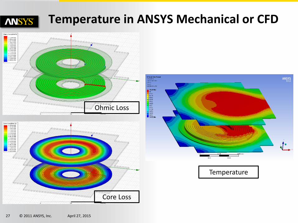
Temperature in ANSYS Mechanical or CFD
Core Loss
Ohmic Loss
Temperature
© 2012 ANSYS, Inc. April 27, 201528
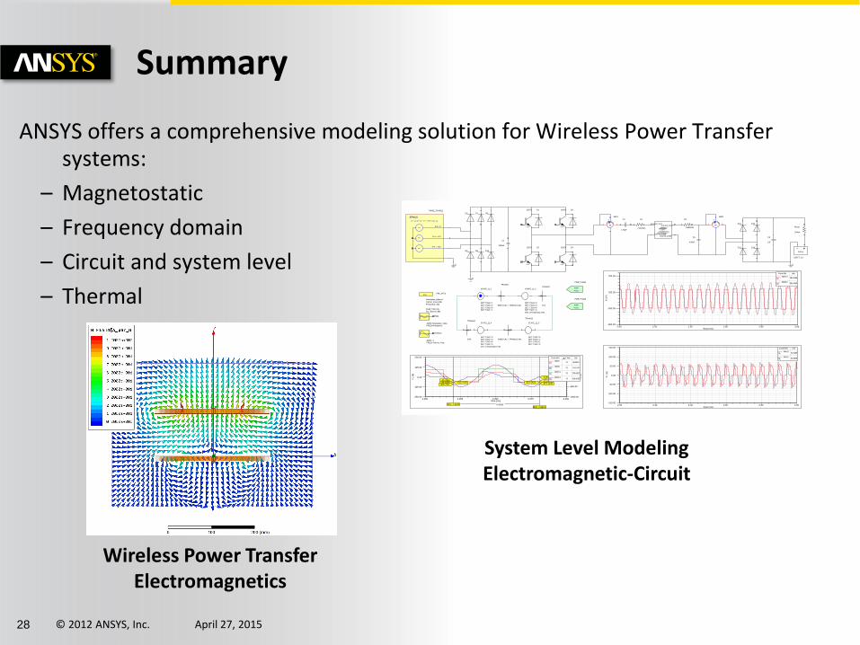
Summary
ANSYS offers a comprehensive modeling solution for Wireless Power Transfer systems:
– Magnetostatic
– Frequency domain
– Circuit and system level
– Thermal
Wireless Power TransferElectromagnetics
System Level ModelingElectromagnetic-Circuit
0
0
0
R1
7.2mOhm
R2
3.6mOhm
Cs
1.72uF
Cp
4.96uF
Rload
13ohm
W
+
WM1
W
+
WM2
D4
D3
D2
D1
IGBT4
IGBT3
IGBT2
IGBT1
C1
1000uF
TRANS4
DT4
TRANS3
SINE1.VAL > TRIANG1.VAL
TRANS2
DT1
TRANS1
SINE1.VAL < TRIANG1.VAL
STATE_11_4
SET: TSV4:=0
SET: TSV3:=0SET: TSV2:=0
SET: TSV1:=0
DEL: DT4##Dead_Time
STATE_11_3
SET: TSV4:=0
SET: TSV3:=1SET: TSV2:=1
SET: TSV1:=0
STATE_11_2
SET: TSV4:=0
SET: TSV3:=0
SET: TSV2:=0SET: TSV1:=0
DEL: DT1##Dead_Time
STATE_11_1
SET: TSV4:=1
SET: TSV3:=0
SET: TSV2:=0SET: TSV1:=1
TRIANG1
AMPL=1FREQ=Carrier_Freq
SINE1
AMPL=Modulation_IndexFREQ=Frequency
ICA:FML_INIT1
Modulation_Index:=0
Carrier_Freq:=20k
Frequency:=20k
DC_Source:=400
Dead_Time:=2u
~
3PHAS
~
~
A * sin (2 * pi * f * t + PHI + phi_u)
PHI = 0°
PHI = -120°
PHI = -240°
THREE_PHASE1
D5
D6
D7
D8
D9
D10 Battery
- +
LBATT_A1
D11
D12
D13
D14
C2
1uF
2.00 2.20 2.40 2.60 2.80 3.00Time [ms]
-150.00
-100.00
-50.00
0.00
50.00
100.00
150.00
Y1 [
A]
Curve Info rms
WM1.ITR 41.6165
WM2.ITR 34.8648
2.00 2.20 2.40 2.60 2.80 3.00Time [ms]
-800.00
-300.00
200.00
700.00
Y1 [
V]
Curve Info rms
WM1.VTR 281.0066
WM2.VTR 321.9453
2.900 2.925 2.950 2.975 3.000Time [ms]
-250.00
-125.00
0.00
125.00
250.00
Y1 [
A]
-1000.00
-500.00
0.00
500.00
873.02
Y2 [
V]
MX1: 2.9200
MX2: 2.9811
-408.7847-315.0105-64.8250
-40.2840
-377.1247-319.5653 -53.6971
-0.0037
0.0610
Curve Info Y Axis rms
WM1.ITR Y1 38.9542
WM2.ITR Y1 34.1140
WM1.VTR Y2 276.0822
WM2.VTR Y2 316.6292
PWR
Probe
PWR_Probe1
Current_1:srcCurrent_2:src
Current_1:snkCurrent_2:snk
PWR
Probe
PWR_Probe2