Embed Size (px)
DESCRIPTION
ece projects
Citation preview

WIRELESS ELECTRONIC
NOTICE BOARD USING GSM
1
CONTENTS
CHAPTER NO DESCRIPTION PAGE NO
1 ABSTRACT 4
2 INTRODUCTION 4
3 BLOCK DIAGRAM 5
4 BLOCK DIAGRAM DESCRIPTION
4.1 GSM MODEM 54.2 MICROCONTROLLER 64.3 LCD 6
5 COMPONENTS’ DETAILED EXPLANATION
5.1 MICROCONTROLLER 6 5.2 LCD INTERFACING 30 5.3 GSM MODEM 32 5.4 MAX 232 36
6 PCB DESIGN
6.1 INTRODUCTION 37 6.2 MANUFACTURING 37 6.3 SOFTWARE 37
6.4 PANELISATION 37 6.5 DRILLING 37
6.6 PLATING 38 6.7 ETCHING 38 6.8 SOLDER MASK 38
6.9 HOT AIR LEVELING 38
2

CHAPTER NO DESCRIPTION PAGE NO SOFTWARE
7 SOFTWARE TOOLS 7.1 KEIL 39 7.2 ASSEMBLING & RUNNING 42
AN 8051
8 OVERALL CIRCUIT DIAGRAM
9 OVERALL CIRCUIT DIAGRAM DESCRIPTION
10 ADVANTAGES 44
11 APPLICATIONS 44
12 CONCLUSION 44
13 BIBLIOGRAPHY 44
3

1. ABSTRACTNotice Board is primary thing in any institution / organization or public utility
places like bus stations, railway stations and parks. But sticking various notices day-to-day is a difficult process. This project deals with an advanced wireless notice board.
The main objective of this project is to develop a wireless notice board that displays messages sent from the user’s mobile. When a user sends a message from his mobile phone, it is received by a SIM loaded GSM modem at the receiver unit. The GSM modem is duly interfaced through level shifter IC for establishing RS232 communication protocol to the microcontroller. The message so received is thus sent to the microcontroller that further displays it on electronic notice board which is equipped with a LCD display interfaced to a microcontroller from 8051 family duly powered by a regulated power supply from mains supply of 230 volt ac.
Further development to this project can be done by providing message storage facility by non-volatile memory i.e. EEPROM attached to the microcontroller for retrieval of old messages if required. It can also be expanded to a bigger LCD screen.
2. Introduction:
Wireless communication has announced its arrival on big stage and the world is going mobile. We want to control everything and without moving an inch. This remote control electronic notice board is possible through Embedded systems. The use of "Embedded system in communication" has given rise to many interesting applications that ensures comfort and safety to human life. GSM(Global System for Mobile Communication) is globally accessed by more than 212 countries and territories. Global system for mobile communication is optimized for duplex voice telephony. GSM, initially developed for the replacement of first generation (1G) technology, now it is upgraded for second generation (2G) technology and third generation (3G) technology
In this technical paper sms based wireless e-notice board explains how to establish an effective and reliable communication between a mobile phone and a microcontroller using GSM modem. This GSM based e-notice board has various applications used in several domains including banks, stoke exchanges, traffic control, public advertisements, educational sector i.e., in schools and colleges etc. In all the above mentioned applications we will use a GSM MODEM, but with a little change in hardware. Along with this I will explain you how this applications are used in low time-to-market and how to upgrade the software resulting low NRE(Non recurring Engineering).This technical paper plays a prominent role in the state-of-the-art scenario to develop authentic and pocket friendly products where the real time market is relentlessly shrinking.
4
3. BLOCK DIAGRAM
4. Block Explanation:
4.1GSM modem:
Here GSM modem is used to send sms to the distance location.
5

4.2 Microcontroller :
Microcontroller will get the data from the user via GSM modem and display the text in the LCD.
4.3 LCD:
Here LCD is interfaced with the controller to view the text which is send by the user at any remote location.
5. COMPONENTS’ DETAILED EXPLANATION
5.1 MICROCONTROLLER
A microcontroller (also MCU or µC) is a functional computer system-on-a-chip. It contains a processor core, memory, and programmable input/output peripherals. Microcontrollers include an integrated CPU, memory (a small amount of RAM, program memory, or both) and peripherals capable of input and output. Microcontrollers are used in automatically controlled products and devices.
BASICS:A designer will use a Microcontroller to
Gather input from various sensors Process this input into a set of actions Use the output mechanisms on the Microcontroller to do something useful.
MEMORY TYPES:
RAM: Random access memory. Ram is a volatile (change) memory. It general purpose memory that can store data or programs. Ex: hard disk, USB device.
ROM: Read only memory. Rom is a non volatile memory. This is typically that is programmed at the factory to have certain values it cannot
be changed. Ex: cd...
6

ARCHITECTURE OF AT89S52
7
8051 Architecture:
8051 Architecture contains the following: CPU ALU I/O ports RAM ROM 2 Timers/Counters General Purpose registers Special Function registers Crystal Oscillators Serial ports Interrupts PSW Program Counter Stack pointer
8051 Addressing Modes
An "addressing mode" refers to how you are addressing a given memory location. In summary, the addressing modes are as follows, with an example of each:
Immediate Addressing MOV A,#20hDirect Addressing MOV A,30hIndirect Addressing MOV A,@R0External Direct MOVX A,@DPTRCode Indirect MOVC A,@A+DPTR
Each of these addressing modes provides important flexibility.
Immediate Addressing
Immediate addressing is so-named because the value to be stored in memory immediately follows the operation code in memory. That is to say, the instruction itself dictates what value will be stored in memory.
For example, the instruction:
MOV A,#20h This instruction uses Immediate Addressing because the Accumulator will be loaded with the value that immediately follows; in this case 20 (hexidecimal).
8

Immediate addressing is very fast since the value to be loaded is included in the instruction. However, since the value to be loaded is fixed at compile-time it is not very flexible.
Direct Addressing
Direct addressing is so-named because the value to be stored in memory is obtained by directly retrieving it from another memory location. For example:
MOV A,30h This instruction will read the data out of Internal RAM address 30 (hexidecimal) and store it in the Accumulator.
Direct addressing is generally fast since, although the value to be loaded isn’t included in the instruction, it is quickly accessable since it is stored in the 8051’s Internal RAM. It is also much more flexible than Immediate Addressing since the value to be loaded is whatever is found at the given address--which may be variable.
Also, it is important to note that when using direct addressing any instruction which refers to an address between 00h and 7Fh is referring to Internal Memory. Any instruction which refers to an address between 80h and FFh is referring to the SFR control registers that control the 8051 microcontroller itself.
The obvious question that may arise is, "If direct addressing an address from 80h through FFh refers to SFRs, how can I access the upper 128 bytes of Internal RAM that are available on the 8052?" The answer is: You can’t access them using direct addressing. As stated, if you directly refer to an address of 80h through FFh you will be referring to an SFR. However, you may access the 8052’s upper 128 bytes of RAM by using the next addressing mode, "indirect addressing."
Indirect Addressing
Indirect addressing is a very powerful addressing mode which in many cases provides an exceptional level of flexibility. Indirect addressing is also the only way to access the extra 128 bytes of Internal RAM found on an 8052.
Indirect addressing appears as follows:
MOV A,@R0
9

This instruction causes the 8051 to analyze the value of the R0 register. The 8051 will then load the accumulator with the value from Internal RAM which is found at the address indicated by R0.
For example, let’s say R0 holds the value 40h and Internal RAM address 40h holds the value 67h. When the above instruction is executed the 8051 will check the value of R0. Since R0 holds 40h the 8051 will get the value out of Internal RAM address 40h (which holds 67h) and store it in the Accumulator. Thus, the Accumulator ends up holding 67h.
Indirect addressing always refers to Internal RAM; it never refers to an SFR. Thus, in a prior example we mentioned that SFR 99h can be used to write a value to the serial port. Thus one may think that the following would be a valid solution to write the value ‘1’ to the serial port:
MOV R0,#99h ;Load the address of the serial portMOV @R0,#01h ;Send 01 to the serial port -- WRONG!!
This is not valid. Since indirect addressing always refers to Internal RAM these two instructions would write the value 01h to Internal RAM address 99h on an 8052. On an 8051 these two instructions would produce an undefined result since the 8051 only has 128 bytes of Internal RAM.
External Direct
External Memory is accessed using a suite of instructions which use what I call "External Direct" addressing. I call it this because it appears to be direct addressing, but it is used to access external memory rather than internal memory.
There are only two commands that use External Direct addressing mode:
MOVXA,@DPTRMOVX @DPTR,A
As you can see, both commands utilize DPTR. In these instructions, DPTR must first be loaded with the address of external memory that you wish to read or write. Once DPTR holds the correct external memory address, the first command will move the contents of that external memory address into the Accumulator. The second command will do the opposite: it will allow you to write the value of the Accumulator to the external memory address pointed to by DPTR.
10

External Indirect
External memory can also be accessed using a form of indirect addressing which I call External Indirect addressing. This form of addressing is usually only used in relatively small projects that have a very small amount of external RAM. An example of this addressing mode is:
MOVX @R0,A Once again, the value of R0 is first read and the value of the Accumulator is written to that address in External RAM. Since the value of @R0 can only be 00h through FFh the project would effectively be limited to 256 bytes of External RAM. There are relatively simple hardware/software tricks that can be implemented to access more than 256 bytes of memory using External Indirect addressing; however, it is usually easier to use External Direct addressing if your project has more than 256 bytes of External RAM.
8051 Program Flow
When an 8051 is first initialized, it resets the PC to 0000h. The 8051 then begins to execute instructions sequentially in memory unless a program instruction causes the PC to be otherwise altered. There are various instructions that can modify the value of the PC; specifically, conditional branching instructions, direct jumps and calls, and "returns" from subroutines. Additionally, interrupts, when enabled, can cause the program flow to deviate from its otherwise sequential scheme.
Conditional Branching
The 8051 contains a suite of instructions which, as a group, are referred to as "conditional branching" instructions. These instructions cause program execution to follow a non-sequential path if a certain condition is true.
Take, for example, the JB instruction. This instruction means "Jump if Bit Set." An example of the JB instruction might be:
JB 45h,HELLONOP
HELLO: ....In this case, the 8051 will analyze the contents of bit 45h. If the bit is set program execution will jump immediately to the label HELLO, skipping the NOP instruction. If the bit is not set the conditional branch fails and program execution continues, as usual, with the NOP instruction which follows.
11

Conditional branching is really the fundamental building block of program logic since all "decisions" are accomplished by using conditional branching. Conditional branching can be thought of as the "IF...THEN" structure in 8051 assembly language.
An important note worth mentioning about conditional branching is that the program may only branch to instructions located within 128 bytes prior to or 127 bytes following the address which follows the conditional branch instruction. This means that in the above example the label HELLO must be within +/- 128 bytes of the memory address which contains the conditional branching instruction.
Direct Jumps
While conditional branching is extremely important, it is often necessary to make a direct branch to a given memory location without basing it on a given logical decision. This is equivalent to saying "Goto" in BASIC. In this case you want the program flow to continue at a given memory address without considering any conditions.
This is accomplished in the 8051 using "Direct Jump and Call" instructions. As illustrated in the last paragraph, this suite of instructions causes program flow to change unconditionally.
Consider the example:
LJMP NEW_ADDRESS...
NEW_ADDRESS: ....The LJMP instruction in this example means "Long Jump." When the 8051 executes this instruction the PC is loaded with the address of NEW_ADDRESS and program execution continues sequentially from there.
The obvious difference between the Direct Jump and Call instructions and the conditional branching is that with Direct Jumps and Calls program flow always changes. With conditional branching program flow only changes if a certain condition is true.
There are two other instructions which cause a direct jump to occur: the SJMP and AJMP commands. Functionally, these two commands perform the exact same function as the LJMP command--that is to say, they always cause program flow to continue at the address indicated by the command.
12
However, SJMP and AJMP differ in the following ways:
The SJMP command, like the conditional branching instructions, can only jump to an address within +/- 128 bytes of the SJMP command.
The AJMP command can only jump to an address that is in the same 2k block of memory as the AJMP command. That is to say, if the AJMP command is at code memory location 650h, it can only do a jump to addresses 0000h through 07FFh (0 through 2047, decimal).
You may be asking yourself, "Why would I want to use the SJMP or AJMP command which have restrictions as to how far they can jump if they do the same thing as the LJMP command which can jump anywhere in memory?" The answer is simple: The LJMP command requires three bytes of code memory whereas both the SJMP and AJMP commands require only two. Thus, if you are developing an application that has memory restrictions you can often save quite a bit of memory using the 2-byte AJMP/SJMP instructions instead of the 3-byte instruction.
Recently, I wrote a program that required 2100 bytes of memory but I had a memory restriction of 2k (2048 bytes). I did a search/replace changing all LJMPs to AJMPs and the program shrunk downto 1950 bytes. Thus, without changing any logic whatsoever in my program I saved 150 bytes and was able to meet my 2048 byte memory restriction.
NOTE: Some quality assemblers will actually do the above conversion for you automatically. That is, they’ll automatically change your LJMPs to SJMPs whenever possible. This is a nifty and very powerful capability that you may want to look for in an assembler if you plan to develop many projects that have relatively tight memory restrictions.
Direct Calls
Another operation that will be familiar to seasoned programmers is the LCALL instruction. This is similar to a "Gosub" command in Basic.
When the 8051 executes an LCALL instruction it immediately pushes the current Program Counter onto the stack and then continues executing code at the address indicated by the LCALL instruction.
Returns from Routines
Another structure that can cause program flow to change is the "Return from Subroutine" instruction, known as RET in 8051 Assembly Language.
13

The RET instruction, when executed, returns to the address following the instruction that called the given subroutine. More accurately, it returns to the address that is stored on the stack.
The RET command is direct in the sense that it always changes program flow without basing it on a condition, but is variable in the sense that where program flow continues can be different each time the RET instruction is executed depending on from where the subroutine was called originally.
Interrupts
An interrupt is a special feature which allows the 8051 to provide the illusion of "multi-tasking," although in reality the 8051 is only doing one thing at a time. The word "interrupt" can often be subsituted with the word "event."
An interrupt is triggered whenever a corresponding event occurs. When the event occurs, the 8051 temporarily puts "on hold" the normal execution of the program and executes a special section of code referred to as an interrupt handler. The interrupt handler performs whatever special functions are required to handle the event and then returns control to the 8051 at which point program execution continues as if it had never been interrupted.
The topic of interrupts is somewhat tricky and very important. For that reason, an entire chapter will be dedicated to the topic. For now, suffice it to say that Interrupts can cause program flow to change.
8051 Tutorial: Instruction Set, Timing, and Low-Level Info
In order to understand--and better make use of--the 8051, it is necessary to understand some underlying information concerning timing.
The 8051 operates based on an external crystal. This is an electrical device which, when energy is applied, emits pulses at a fixed frequency. One can find crystals of virtually any frequency depending on the application requirements. When using an 8051, the most common crystal frequencies are 12 megahertz and 11.059 megahertz--with 11.059 being much more common. Why would anyone pick such an odd-ball frequency? There’s a real reason for it--it has to do with generating baud rates and we’ll talk more about it in the Serial Communication chapter. For the remainder of this discussion we’ll assume that we’re using an 11.059Mhz crystal.
Microcontrollers (and many other electrical systems) use crystals to syncrhronize operations. The 8051 uses the crystal for precisely that: to synchronize it’s operation.
14

Effectively, the 8051 operates using what are called "machine cycles." A single machine cycle is the minimum amount of time in which a single 8051 instruction can be executed. although many instructions take multiple cycles.
A cycle is, in reality, 12 pulses of the crystal. That is to say, if an instruction takes one machine cycle to execute, it will take 12 pulses of the crystal to execute. Since we know the crystal is pulsing 11,059,000 times per second and that one machine cycle is 12 pulses, we can calculate how many instruction cycles the 8051 can execute per second:
11,059,000 / 12 = 921,583 This means that the 8051 can execute 921,583 single-cycle instructions per second. Since a large number of 8051 instructions are single-cycle instructions it is often considered that the 8051 can execute roughly 1 million instructions per second, although in reality it is less--and, depending on the instructions being used, an estimate of about 600,000 instructions per second is more realistic.
For example, if you are using exclusively 2-cycle instructions you would find that the 8051 would execute 460,791 instructions per second. The 8051 also has two really slow instructions that require a full 4 cycles to execute--if you were to execute nothing but those instructions you’d find performance to be about 230,395 instructions per second.
It is again important to emphasize that not all instructions execute in the same amount of time. The fastest instructions require one machine cycle (12 crystal pulses), many others require two machine cycles (24 crystal pulses), and the two very slow math operations require four machine cycles (48 crystal pulses).
NOTE: Many 8051 derivative chips change instruction timing. For example, many optimized versions of the 8051 execute instructions in 4 oscillator cycles instead of 12; such a chip would be effectively 3 times faster than the 8051 when used with the same 11.059 Mhz crystal.
Since all the instructions require different amounts of time to execute a very obvious question comes to mind: How can one keep track of time in a time-critical application if we have no reference to time in the outside world?
Luckily, the 8051 includes timers which allow us to time events with high precision--which is the topic of the next chapter.
15

8051 Timers
The 8051 comes equipped with two timers, both of which may be controlled, set, read, and configured individually. The 8051 timers have three general functions: 1) Keeping time and/or calculating the amount of time between events, 2) Counting the events themselves, or 3) Generating baud rates for the serial port.
The three timer uses are distinct so we will talk about each of them separately. The first two uses will be discussed in this chapter while the use of timers for baud rate generation will be discussed in the chapter relating to serial ports.
How does a timer count?
How does a timer count? The answer to this question is very simple: A timer always counts up. It doesn’t matter whether the timer is being used as a timer, a counter, or a baud rate generator: A timer is always incremented by the microcontroller.
Programming Tip: Some derivative chips actually allow the program to configure whether the timers count up or down. However, since this option only exists on some derivatives it is beyond the scope of this tutorial which is aimed at the standard 8051. It is only mentioned here in the event that you absolutely need a timer to count backwards, you will know that you may be able to find an 8051-compatible microcontroller that does it.
USING TIMERS TO MEASURE TIME
Obviously, one of the primary uses of timers is to measure time. We will discuss this use of timers first and will subsequently discuss the use of timers to count events. When a timer is used to measure time it is also called an "interval timer" since it is measuring the time of the interval between two events.
How long does a timer take to count?
First, it’s worth mentioning that when a timer is in interval timer mode (as opposed to event counter mode) and correctly configured, it will increment by 1 every machine cycle. As you will recall from the previous chapter, a single machine cycle consists of 12 crystal pulses. Thus a running timer will be incremented:
11,059,000 / 12 = 921,583 921,583 times per second. Unlike instructions--some of which require 1 machine cycle, others 2, and others 4--the timers are consistent: They will always be incremented once per machine cycle.
16

Thus if a timer has counted from 0 to 50,000 you may calculate: 50,000 / 921,583 = .0542
.0542 seconds have passed. In plain English, about half of a tenth of a second, or one-twentieth of a second.
Obviously it’s not very useful to know .0542 seconds have passed. If you want to execute an event once per second you’d have to wait for the timer to count from 0 to 50,000 18.45 times. How can you wait "half of a time?" You can’t. So we come to another important calculation.
Let’s say we want to know how many times the timer will be incremented in .05 seconds. We can do simple multiplication:
.05 * 921,583 = 46,079.15. This tells us that it will take .05 seconds (1/20th of a second) to count from 0 to 46,079. Actually, it will take it .049999837 seconds--so we’re off by .000000163 seconds--however, that’s close enough for government work. Consider that if you were building a watch based on the 8051 and made the above assumption your watch would only gain about one second every 2 months. Again, I think that’s accurate enough for most applications--I wish my watch only gained one second every two months!
Obviously, this is a little more useful. If you know it takes 1/20th of a second to count from 0 to 46,079 and you want to execute some event every second you simply wait for the timer to count from 0 to 46,079 twenty times; then you execute your event, reset the timers, and wait for the timer to count up another 20 times. In this manner you will effectively execute your event once per second, accurate to within thousandths of a second.
Thus, we now have a system with which to measure time. All we need to review is how to control the timers and initialize them to provide us with the information we need.
Timer SFRs
As mentioned before, the 8051 has two timers which each function essentially the same way. One timer is TIMER0 and the other is TIMER1. The two timers share two SFRs (TMOD and TCON) which control the timers, and each timer also has two SFRs dedicated solely to itself (TH0/TL0 and TH1/TL1).
We’ve given SFRs names to make it easier to refer to them, but in reality an SFR has a numeric address. It is often useful to know the numeric address that corresponds to an SFR name.
17

The SFRs relating to timers are:
SFR Name Description SFR Address
TH0 Timer 0 High Byte 8Ch
TL0 Timer 0 Low Byte 8Ah
TH1 Timer 1 High Byte 8Dh
TL1 Timer 1 Low Byte 8Bh
TCON Timer Control 88h
TMOD Timer Mode 89h
When you enter the name of an SFR into an assembler, it internally converts it to a number. For example, the command:
MOV TH0,#25h moves the value 25h into the TH0 SFR. However, since TH0 is the same as SFR address 8Ch this command is equivalent to:
MOV 8Ch,#25h Now, back to the timers. First, let’s talk about Timer 0.
Timer 0 has two SFRs dedicated exclusively to itself: TH0 and TL0. Without making things too complicated to start off with, you may just think of this as the high and low byte of the timer. That is to say, when Timer 0 has a value of 0, both TH0 and TL0 will contain 0. When Timer 0 has the value 1000, TH0 will hold the high byte of the value (3 decimal) and TL0 will contain the low byte of the value (232 decimal). Reviewing low/high byte notation, recall that you must multiply the high byte by 256 and add the low byte to calculate the final value. That is to say:
TH0 * 256 + TL0 = 10003 * 256 + 232 = 1000
Timer 1 works the exact same way, but it’s SFRs are TH1 and TL1. Since there are only two bytes devoted to the value of each timer it is apparent that the maximum value a timer may have is 65,535. If a timer contains the value 65,535 and is subsequently incremented, it will reset--or overflow--back to 0.
The TMOD SFR
Let’s first talk about our first control SFR: TMOD (Timer Mode). The TMOD SFR is used to control the mode of operation of both timers. Each bit of the SFR gives the microcontroller specific information concerning how to run a timer.
18

The high four bits (bits 4 through 7) relate to Timer 1 whereas the low four bits (bits 0 through 3) perform the exact same functions, but for timer 0.
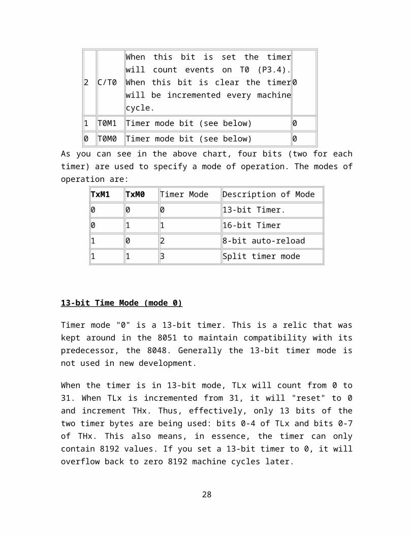
The individual bits of TMOD have the following functions: TMOD (89h) SFR
Bit Name Explanation of Function Timer
7 GATE1When this bit is set the timer will only run when INT1 (P3.3) is high. When this bit is clear the timer will run regardless of the state of INT1.
1
6 C/T1When this bit is set the timer will count events on T1 (P3.5). When this bit is clear the timer will be incremented every machine cycle.
1
5 T1M1 Timer mode bit (see below) 1
4 T1M0 Timer mode bit (see below) 1
3 GATE0When this bit is set the timer will only run when INT0 (P3.2) is high. When this bit is clear the timer will run regardless of the state of INT0.
0
2 C/T0When this bit is set the timer will count events on T0 (P3.4). When this bit is clear the timer will be incremented every machine cycle.
0
1 T0M1 Timer mode bit (see below) 0
0 T0M0 Timer mode bit (see below) 0
As you can see in the above chart, four bits (two for each timer) are used to specify a mode of operation. The modes of operation are:
TxM1 TxM0 Timer Mode Description of Mode
0 0 0 13-bit Timer.
0 1 1 16-bit Timer
1 0 2 8-bit auto-reload
1 1 3 Split timer mode
13-bit Time Mode (mode 0)
Timer mode "0" is a 13-bit timer. This is a relic that was kept around in the 8051 to maintain compatibility with its predecessor, the 8048. Generally the 13-bit timer mode is not used in new development.
19
When the timer is in 13-bit mode, TLx will count from 0 to 31. When TLx is incremented from 31, it will "reset" to 0 and increment THx. Thus, effectively, only 13 bits of the two timer bytes are being used: bits 0-4 of TLx and bits 0-7 of THx. This also means, in essence, the timer can only contain 8192 values. If you set a 13-bit timer to 0, it will overflow back to zero 8192 machine cycles later.
Again, there is very little reason to use this mode and it is only mentioned so you won’t be surprised if you ever end up analyzing archaeic code which has been passed down through the generations (a generation in a programming shop is often on the order of about 3 or 4 months).
16-bit Time Mode (mode 1)
Timer mode "1" is a 16-bit timer. This is a very commonly used mode. It functions just like 13-bit mode except that all 16 bits are used. TLx is incremented from 0 to 255. When TLx is incremented from 255, it resets to 0 and causes THx to be incremented by 1. Since this is a full 16-bit timer, the timer may contain up to 65536 distinct values. If you set a 16-bit timer to 0, it will overflow back to 0 after 65,536 machine cycles.
8-bit Time Mode (mode 2)
Timer mode "2" is an 8-bit auto-reload mode. What is that, you may ask? Simple. When a timer is in mode 2, THx holds the "reload value" and TLx is the timer itself. Thus, TLx starts counting up. When TLx reaches 255 and is subsequently incremented, instead of resetting to 0 (as in the case of modes 0 and 1), it will be reset to the value stored in THx.
For example, let’s say TH0 holds the value FDh and TL0 holds the value FEh. If we were to watch the values of TH0 and TL0 for a few machine cycles this is what we’d see:
Machine Cycle TH0 Value TL0 Value
1 FDh FEh
2 FDh FFh
3 FDh FDh
4 FDh FEh
5 FDh FFh
6 FDh FDh
7 FDh FEh
20

As you can see, the value of TH0 never changed. In fact, when you use mode 2 you almost always set THx to a known value and TLx is the SFR that is constantly incremented.
What’s the benefit of auto-reload mode? Perhaps you want the timer to always have a value from 200 to 255. If you use mode 0 or 1, you’d have to check in code to see if the timer had overflowed and, if so, reset the timer to 200. This takes precious instructions of execution time to check the value and/or to reload it. When you use mode 2 the microcontroller takes care of this for you. Once you’ve configured a timer in mode 2 you don’t have to worry about checking to see if the timer has overflowed nor do you have to worry about resetting the value--the microcontroller hardware will do it all for you.
The auto-reload mode is very commonly used for establishing a baud rate which we will talk more about in the Serial Communications chapter.
Split Timer Mode (mode 3)
Timer mode "3" is a split-timer mode. When Timer 0 is placed in mode 3, it essentially becomes two separate 8-bit timers. That is to say, Timer 0 is TL0 and Timer 1 is TH0. Both timers count from 0 to 255 and overflow back to 0. All the bits that are related to Timer 1 will now be tied to TH0.
While Timer 0 is in split mode, the real Timer 1 (i.e. TH1 and TL1) can be put into modes 0, 1 or 2 normally--however, you may not start or stop the real timer 1 since the bits that do that are now linked to TH0. The real timer 1, in this case, will be incremented every machine cycle no matter what.
The only real use I can see of using split timer mode is if you need to have two separate timers and, additionally, a baud rate generator. In such case you can use the real Timer 1 as a baud rate generator and use TH0/TL0 as two separate timers.
The TCON SFR Finally, there’s one more SFR that controls the two timers and provides valuable information about them.
21

The TCON SFR has the following structure: TCON (88h) SFR
Bit NameBit Address
Explanation of Function Timer
7 TF1 8FhTimer 1 Overflow. This bit is set by the microcontroller when Timer 1 overflows.
1
6 TR1 8EhTimer 1 Run. When this bit is set Timer 1 is turned on. When this bit is clear Timer 1 is off.
1
5 TF0 8DhTimer 0 Overflow. This bit is set by the microcontroller when Timer 0 overflows.
0
4 TR0 8ChTimer 0 Run. When this bit is set Timer 0 is turned on. When this bit is clear Timer 0 is off.
0
As you may notice, we’ve only defined 4 of the 8 bits. That’s because the other 4 bits of the SFR don’t have anything to do with timers--they have to do with Interrupts and they will be discussed in the chapter that addresses interrupts.
A new piece of information in this chart is the column "bit address." This is because this SFR is "bit-addressable." What does this mean? It means if you want to set the bit TF1--which is the highest bit of TCON--you could execute the command:
MOV TCON, #80h ... or, since the SFR is bit-addressable, you could just execute the command:
SETB TF1 This has the benefit of setting the high bit of TCON without changing the value of any of the other bits of the SFR. Usually when you start or stop a timer you don’t want to modify the other values in TCON, so you take advantage of the fact that the SFR is bit-addressable.
Initializing a Timer
Now that we’ve discussed the timer-related SFRs we are ready to write code that will initialize the timer and start it running.
As you’ll recall, we first must decide what mode we want the timer to be in. In this case we want a 16-bit timer that runs continuously; that is to say, it is not dependent on any external pins.
We must first initialize the TMOD SFR. Since we are working with timer 0 we will be using the lowest 4 bits of TMOD. The first two bits, GATE0 and C/T0 are both 0 since we want the timer to be independent of the external pins.
22

16-bit mode is timer mode 1 so we must clear T0M1 and set T0M0. Effectively, the only bit we want to turn on is bit 0 of TMOD. Thus to initialize the timer we execute the instruction:
MOV TMOD,#01h Timer 0 is now in 16-bit timer mode. However, the timer is not running. To start the timer running we must set the TR0 bit We can do that by executing the instruction:
SETB TR0 Upon executing these two instructions timer 0 will immediately begin counting, being incremented once every machine cycle (every 12 crystal pulses).
Reading the Timer
There are two common ways of reading the value of a 16-bit timer; which you use depends on your specific application. You may either read the actual value of the timer as a 16-bit number, or you may simply detect when the timer has overflowed.
Reading the value of a Timer
If your timer is in an 8-bit mode--that is, either 8-bit AutoReload mode or in split timer mode--then reading the value of the timer is simple. You simply read the 1-byte value of the timer and you’re done.
However, if you’re dealing with a 13-bit or 16-bit timer the chore is a little more complicated. Consider what would happen if you read the low byte of the timer as 255, then read the high byte of the timer as 15. In this case, what actually happened was that the timer value was 14/255 (high byte 14, low byte 255) but you read 15/255. Why? Because you read the low byte as 255. But when you executed the next instruction a small amount of time passed--but enough for the timer to increment again at which time the value rolled over from 14/255 to 15/0. But in the process you’ve read the timer as being 15/255. Obviously there’s a problem there.
You read the high byte of the timer, then read the low byte, then read the high byte again. If the high byte read the second time is not the same as the high byte read the first time you repeat the cycle. In code, this would appear as:
REPEAT: MOV A,TH0MOV R0,TL0CJNE A,TH0,REPEAT
23

In this case, we load the accumulator with the high byte of Timer 0. We then load R0 with the low byte of Timer 0. Finally, we check to see if the high byte we read out of Timer 0--which is now stored in the Accumulator--is the same as the current Timer 0 high byte. If it isn’t it means we’ve just "rolled over" and must reread the timer’s value--which we do by going back to REPEAT. When the loop exits we will have the low byte of the timer in R0 and the high byte in the Accumulator.
Another much simpler alternative is to simply turn off the timer run bit (i.e. CLR TR0), read the timer value, and then turn on the timer run bit (i.e. SETB TR0). In that case, the timer isn’t running so no special tricks are necessary. Of course, this implies that your timer will be stopped for a few machine cycles. Whether or not this is tolerable depends on your specific application.
Detecting Timer Overflow
Often it is necessary to just know that the timer has reset to 0. That is to say, you are not particularly interest in the value of the timer but rather you are interested in knowing when the timer has overflowed back to 0.
Whenever a timer overflows from it’s highest value back to 0, the microcontroller automatically sets the TFx bit in the TCON register. This is useful since rather than checking the exact value of the timer you can just check if the TFx bit is set. If TF0 is set it means that timer 0 has overflowed; if TF1 is set it means that timer 1 has overflowed.
We can use this approach to cause the program to execute a fixed delay. As you’ll recall, we calculated earlier that it takes the 8051 1/20th of a second to count from 0 to 46,079. However, the TFx flag is set when the timer overflows back to 0. Thus, if we want to use the TFx flag to indicate when 1/20th of a second has passed we must set the timer initially to 65536 less 46079, or 19,457. If we set the timer to 19,457, 1/20th of a second later the timer will overflow. Thus we come up with the following code to execute a pause of 1/20th of a second:
MOV TH0,#76;High byte of 19,457 (76 * 256 = 19,456)MOV TL0,#01;Low byte of 19,457 (19,456 + 1 = 19,457)MOV TMOD,#01;Put Timer 0 in 16-bit modeSETB TR0;Make Timer 0 start countingJNB TF0,$;If TF0 is not set, jump back to this same instruction
In the above code the first two lines initialize the Timer 0 starting value to 19,457. The next two instructions configure timer 0 and turn it on. Finally, the last instruction JNB TF0,$, reads "Jump, if TF0 is not set, back to this same instruction."
24

The "$" operand means, in most assemblers, the address of the current instruction. Thus as long as the timer has not overflowed and the TF0 bit has not been set the program will keep executing this same instruction. After 1/20th of a second timer 0 will overflow, set the TF0 bit, and program execution will then break out of the loop.
Timing the length of events
The 8051 provides another cool toy that can be used to time the length of events.
For example, let's say we're trying to save electricity in the office and we're interested in how long a light is turned on each day. When the light is turned on, we want to measure time. When the light is turned off we don't. One option would be to connect the lightswitch to one of the pins, constantly read the pin, and turn the timer on or off based on the state of that pin. While this would work fine, the 8051 provides us with an easier method of accomplishing this.
Looking again at the TMOD SFR, there is a bit called GATE0. So far we've always cleared this bit because we wanted the timer to run regardless of the state of the external pins. However, now it would be nice if an external pin could control whether the timer was running or not. It can. All we need to do is connect the lightswitch to pin INT0 (P3.2) on the 8051 and set the bit GATE0. When GATE0 is set Timer 0 will only run if P3.2 is high. When P3.2 is low (i.e., the lightswitch is off) the timer will automatically be stopped.
Thus, with no control code whatsoever, the external pin P3.2 can control whether or not our timer is running or not.
USING TIMERS AS EVENT COUNTERS
We've discussed how a timer can be used for the obvious purpose of keeping track of time. However, the 8051 also allows us to use the timers to count events.
How can this be useful? Let's say you had a sensor placed across a road that would send a pulse every time a car passed over it. This could be used to determine the volume of traffic on the road. We could attach this sensor to one of the 8051's I/O lines and constantly monitor it, detecting when it pulsed high and then incrementing our counter when it went back to a low state. This is not terribly difficult, but requires some code.
25

Let's say we hooked the sensor to P1.0; the code to count cars passing would look something like this:
JNB P1.0,$ ;If a car hasn't raised the signal, keep waitingJB P1.0,$ ;The line is high which means the car is on the sensor right nowINC COUNTER ;The car has passed completely, so we count it
As you can see, it's only three lines of code. But what if you need to be doing other processing at the same time? You can't be stuck in the JNB P1.0,$ loop waiting for a car to pass if you need to be doing other things. Of course, there are ways to get around even this limitation but the code quickly becomes big, complex, and ugly.
Luckily, since the 8051 provides us with a way to use the timers to count events we don't have to bother with it. It is actually painfully easy. We only have to configure one additional bit.
Let's say we want to use Timer 0 to count the number of cars that pass. If you look back to the bit table for the TCON SFR you will there is a bit called "C/T0"--it's bit 2 (TCON.2). Reviewing the explanation of the bit we see that if the bit is clear then timer 0 will be incremented every machine cycle. This is what we've already used to measure time. However, if we set C/T0 timer 0 will monitor the P3.4 line. Instead of being incremented every machine cycle, timer 0 will count events on the P3.4 line. So in our case we simply connect our sensor to P3.4 and let the 8051 do the work. Then, when we want to know how many cars have passed, we just read the value of timer 0--the value of timer 0 will be the number of cars that have passed.
So what exactly is an event? What does timer 0 actually "count?" Speaking at the electrical level, the 8051 counts 1-0 transitions on the P3.4 line. This means that when a car first runs over our sensor it will raise the input to a high ("1") condition. At that point the 8051 will not count anything since this is a 0-1 transition. However, when the car has passed the sensor will fall back to a low ("0") state. This is a 1-0 transition and at that instant the counter will be incremented by 1.
It is important to note that the 8051 checks the P3.4 line each instruction cycle (12 clock cycles). This means that if P3.4 is low, goes high, and goes back low in 6 clock cycles it will probably not be detected by the 8051. This also means the 8051 event counter is only capable of counting events that occur at a maximum of 1/24th the rate of the crystal frequency. That is to say, if the crystal frequency is 12.000 Mhz it can count a maximum of 500,000 events per second (12.000 Mhz * 1/24 = 500,000). If the event being counted occurs more than 500,000 times per second it will not be able to be accurately counted by the 8051.
26

DESCRIPTION OF AT89S52:
The AT89S52 is a low-power, high-performance CMOS 8-bit microcomputer with 4K bytes of Flash programmable and erasable read only memory (PEROM). The device is manufactured using Atmel’s high-density nonvolatile memory technology and is compatible with the industry-standard MCS-51 instruction set and pinout. The on-chip Flash allows the program memory to be reprogrammed in-system or by a conventional nonvolatile memory programmer. By combining a versatile 8-bit CPU with Flash on a monolithic chip, the Atmel AT89S52 is a powerful microcomputer which provides a highly-flexible and cost-effective solution to many embedded control applications.
The AT89S52 provides the following standard features: 4K bytes of Flash, 128 bytes of RAM, 32 I/O lines, two 16-bit timer/counters, five vector two-level interrupt architecture, a full duplex serial port, and on-chip oscillator and clock circuitry. In addition, the AT89S52 is designed with static logic for operation down to zero frequency and supports two software selectable power saving modes. The Idle Mode stops the CPU while allowing the RAM, timer/counters, serial port and interrupt system to continue functioning. The Power-down Mode saves the RAM contents but freezes the oscillator disabling all other chip functions until the next hardware reset.
OSCILLATOR CHARACTERISTICS:XTAL1 and XTAL2 are the input and output, respectively, of an inverting
amplifier which can be configured for use as an on-chip oscillator; Either a quartz crystal or ceramic resonator may be used. To drive the device from an external clock source, XTAL2 should be left unconnected while XTAL1 is driven. There are no requirements on the duty cycle of the external clock signal, since the input to the internal clocking circuitry is through a divide-by-two flip-flop, but minimum and maximum voltage high and low time specifications must be observed.
IDLE MODE:In idle mode, the CPU puts itself to sleep while all the on chip peripherals remain
active. The mode is invoked by software. The content of the on-chip RAM and all the special functions registers remain unchanged during this mode. The idle mode can be terminated by any enabled interrupt or by a hardware reset. It should be noted that when idle is terminated by a hard ware reset, the device normally resumes program execution, from where it left off, up to two machine cycles before the internal reset algorithm takes control. On-chip hardware inhibits access to internal RAM in this event, but access to the port pins is not inhibited. To eliminate the possibility of an unexpected write to a port pin when Idle is terminated by Reset, the instruction following the one that invokes Idle should not be one that writes to a port pin or to external memory.
27
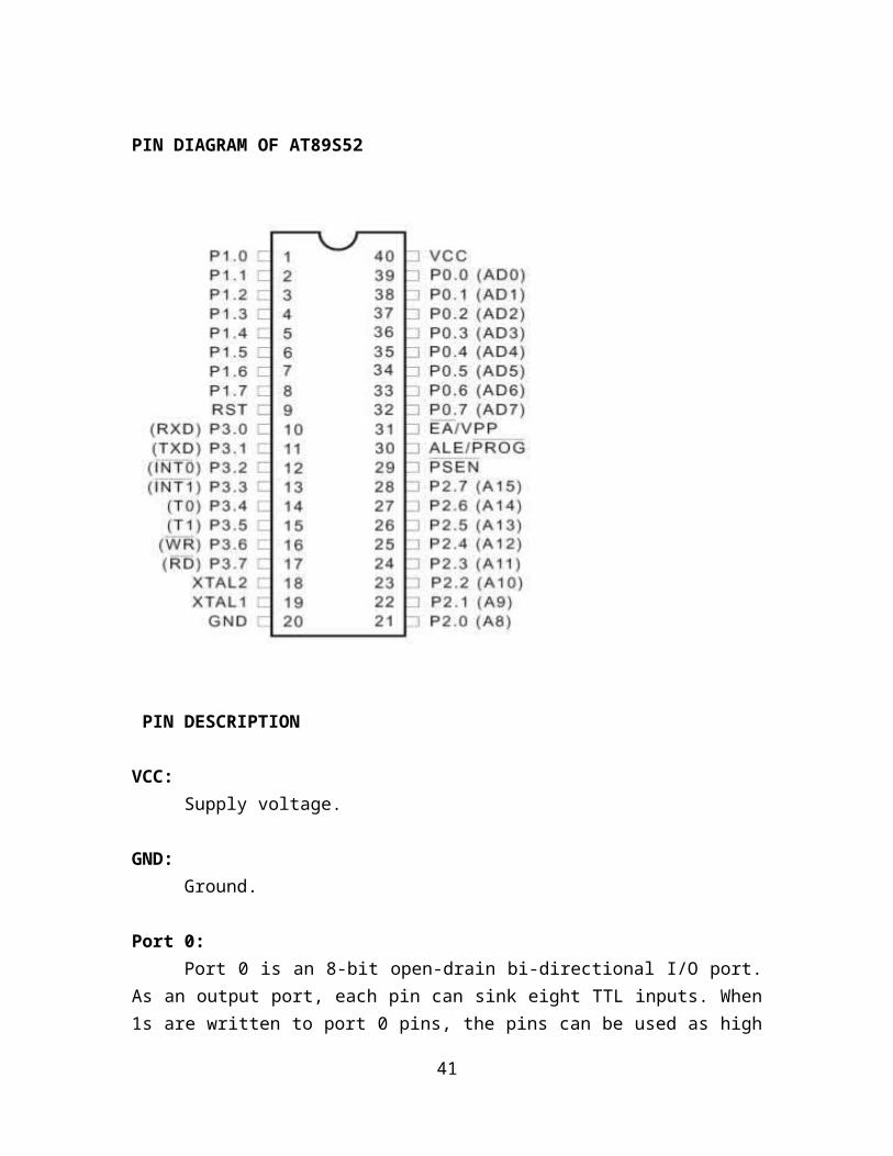
PIN DIAGRAM OF AT89S52
PIN DESCRIPTION
VCC:Supply voltage.
GND:Ground.
Port 0:Port 0 is an 8-bit open-drain bi-directional I/O port. As an output port, each pin
can sink eight TTL inputs. When 1s are written to port 0 pins, the pins can be used as high impedance inputs. Port 0 may also be configured to be the multiplexed low order address/data bus during accesses to external program and data memory. In this mode P0 has internal pull-ups. Port 0 also receives the code bytes during Flash programming, and outputs the code bytes during program verification. External pull-ups are required during program verification.Port 1:
28

Port 1 is an 8-bit bi-directional I/O port with internal pull-ups. The Port 1 output buffers can sink/source four TTL inputs. When 1s are written to Port 1 pins they are pulled high by the internal pull-ups and can be used as inputs. As inputs, Port 1 pins that are externally being pulled low will source current (IIL) because of the internal pull-ups. Port 1 also receives the low-order address bytes during Flash programming and verification.
Port 2:Port 2 is an 8-bit bi-directional I/O port with internal pull-ups. The Port 2 output
buffers can sink/source four TTL inputs. When 1s are written to Port 2 pins they are pulled high by the internal pull-ups and can be used as inputs.Port 2 pins that are externally being pulled low will source current (IIL) because of the internal pull-ups.
RST:Reset input a high on this pin for two machine cycles while the oscillator is
running resets the device.
ALE/PROG:
Address Latch Enable output pulse for latching the low byte of the address during accesses to external memory. This pin is also the program pulse input (PROG) during Flash programming. In normal operation ALE is emitted at a constant rate of 1/6 the oscillator frequency, and may be used for external timing or clocking purposes. Note, however, that one ALE pulse is skipped during each access to external Data Memory.
PSEN:Program Store Enable is the read strobe to external program memory. When the
AT89S52 is executing code from external program memory, PSEN is activated twice each machine cycle, except that two PSEN activations are skipped during each access to external data memory.
EA/VPP:External Access Enable. EA must be strapped to GND in order to enable the
device to fetch code from external program memory locations starting at 0000H up to FFFFH. Note, however, that if lock bit 1 is programmed, EA will be internally latched on reset. EA should be strapped to VCC for internal program executions. This pin also receives the 12volt programming enable voltage (VPP) during Flash programming, for parts that require 12-volt VPP.
XTAL1:
29

Input to the inverting oscillator amplifier and input to the internal clock operating circuit.
XTAL2:Output from the inverting oscillator amplifier.
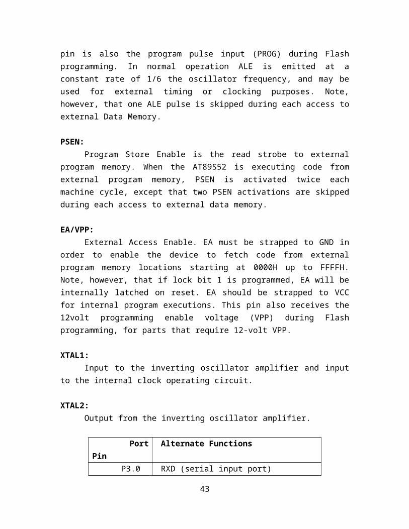
Port Pin Alternate Functions P3.0 P3.1 P3.2 P3.3 P3.4 P3.5 P3.6 P3.7
RXD (serial input port) TXD (serial output port) INT0 (external interrupt 0) INT1 (external interrupt 1) T0 (timer 0 external input) T1 (timer 1 external input) WR (external data memory write strobe) RD (external data memory read strobe)
5.2 LCD interfacing with Microcontrollers
Introduction
The most commonly used Character based LCDs are based on Hitachi's HD44780 controller or other which are compatible with HD44580. In this tutorial, we will discuss about character based LCDs, their interfacing with various microcontrollers, various interfaces (8-bit/4-bit), programming, special stuff and tricks you can do with these simple looking LCDs which can give a new look to your application.For Specs and technical information HD44780 controller
Pin DescriptionThe most commonly used LCDs found in the market today are 1 Line, 2 Line or 4 Line LCDs which have only 1 controller and support at most of 80 charachers, whereas LCDs supporting more than 80 characters make use of 2 HD44780 controllers.
Most LCDs with 1 controller has 14 Pins and LCDs with 2 controller has 16 Pins (two pins are extra in both for back-light LED connections). Pin description is shown in the table below.
30

Figure 1: Character LCD type HD44780 Pin diagram
Pin No. Name DescriptionPin no. 1 VSS Power supply (GND)Pin no. 2 VCC Power supply (+5V)Pin no. 3 VEE Contrast adjust
Pin no. 4 RS0 = Instruction input1 = Data input
Pin no. 5 R/W0 = Write to LCD module1 = Read from LCD module
Pin no. 6 EN Enable signalPin no. 7 D0 Data bus line 0 (LSB)Pin no. 8 D1 Data bus line 1Pin no. 9 D2 Data bus line 2Pin no. 10 D3 Data bus line 3Pin no. 11 D4 Data bus line 4Pin no. 12 D5 Data bus line 5Pin no. 13 D6 Data bus line 6Pin no. 14 D7 Data bus line 7 (MSB)
Table 1: Character LCD pins with 1 Controller
Pin No. Name DescriptionPin no. 1 D7 Data bus line 7 (MSB)Pin no. 2 D6 Data bus line 6Pin no. 3 D5 Data bus line 5Pin no. 4 D4 Data bus line 4Pin no. 5 D3 Data bus line 3Pin no. 6 D2 Data bus line 2
31

Pin no. 7 D1 Data bus line 1Pin no. 8 D0 Data bus line 0 (LSB)Pin no. 9 EN1 Enable signal for row 0 and 1 (1stcontroller)
Pin no. 10 R/W0 = Write to LCD module1 = Read from LCD module
Pin no. 11 RS0 = Instruction input1 = Data input
Pin no. 12 VEE Contrast adjustPin no. 13 VSS Power supply (GND)Pin no. 14 VCC Power supply (+5V)Pin no. 15 EN2 Enable signal for row 2 and 3 (2ndcontroller)Pin no. 16 NC Not Connected
Table 2: Character LCD pins with 2 Controller
5.3 GSM Modem:
A GSM modem is a specialized type of modem which accepts a SIM card, and operates over a subscription to a mobile operator, just like a mobile phone. From the mobile operator perspective, a GSM modem looks just like a mobile phone.
When a GSM modem is connected to a\controller and it allows the controller to use the GSM modem to communicate over the mobile network.
While these GSM modems are most frequently used to provide mobile internet connectivity, many of them can also be used for sending and receiving SMS and MMS messages.
A GSM modem can be a dedicated modem device with a serial, USB connection, or it can be a mobile phone that provides GSM modem capabilities.
For the purpose of this document, the term GSM modem is used as a generic term to refer to any modem that supports one or more of the protocols in the GSM evolutionary family, including the 2.5G technologies GPRS and EDGE (also known as Enhanced Global evolution) is a data system used on top of GSM networks. It provides nearly three times faster speeds than the outdated GPRS system..
32

A GSM modem exposes an interface that allows applications such as SMS to send and receive messages over the modem interface.
To perform these tasks, a GSM modem must support an “extended AT command set” for sending/receiving SMS messages.
GSM modems can be a quick and efficient way to get started with SMS. In most parts of the world, GSM modems are a cost effective solution for receiving SMS messages, because the sender is paying for the message delivery.
A GSM modem can be a dedicated modem device with a serial, USB connection, such as the Falcom Samba 75. (Other manufacturers of dedicated GSM modem devices include Wavecom, Multitech and iTegno.
A GSM modem could also be a standard GSM mobile phone with the appropriate cable and software driver to connect to a serial port or USB port on your computer. Any phone that supports the “extended AT command set” for sending/receiving SMS messages, as defined in ETSI GSM 07.05 and/or 3GPP TS 27.005, can be supported by the Now SMS & MMS Gateway. Note that not all mobile phones support this modem interface.
It should also be noted that not all phones support the modem interface for sending and receiving SMS messages.
In particular, most smart phones, including Blackberries, iPhone, and Windows Mobile devices, do not support this GSM modem interface for sending and receiving SMS messages at all at all.
Additionally, Nokia phones that use the S60 (Series 60) interface, which is Symbian based, only support sending SMS messages via the modem interface, and do not support receiving SMS via the modem interface.
Send SMS using AT commands
Some advanced GSM modems like WaveCom and Multitech, support the SMS text mode. This mode allows you to send SMS messages using AT commands
Check if your GSM phone or modem supports SMS text mode
To check if your modem supports this text mode, you can try the following command:
AT+CMGF=1 <ENTER>(Message Format)
33
If the modem reponds with "OK" this mode is supported. Please note that using this mode it is onluy possible to send simple text messages. It is not possible to send multipart, Unicode, data and other types of messages.
Setting up the modem
If the modem contains a SIM card with is secured with a PIN code, we have to enter this pin code first:
AT+CPIN="0000" <ENTER> (replace 0000 with your PIN code).
Please not that in most cases you have only 3 attemps to set the correct PIN code. After setting the PIN code, wait some seconds before issueing the next command to give the modem some time to register with the GSM network.
In order to send a SMS, the modem has to be put in SMS text mode first using the following command:
AT+CMGF=1 <ENTER>
In text mode there are some additional parameters that can be set. Using the following command we can read the current values:
Sending the message
To send the SMS message, type the following command:
AT+CMGS="9976715594"(send message)CMD1: DB 'AT',0AH,0DH,0CMD2: DB 'AT+CMGF=1',0AH,0DH,0CMD3: DB 'AT+CMGS="9976715594"',0AH,0DH,0CMD41: DB 'vibration detected ',0AH,0DH,0CMD42: DB 'high temperature',0AH,0DH,0CMD43: DB 'motor stop ',0AH,0DH,0CMD5: DB 1AH,0
Receiving SMS using AT commands:
Receiving A GSM phone or modem receives messages automatically. Basically you are just retrieving the messages from the memory of the device or SIM card. To select the message storage used to read the messages from, you have to use the "AT+CPMS"
34

command. You can select one of the following message storages, not all storages are supported on every device.
Storage ID Description
SMRead SMS messages from the SIM card. This storage is supported on every GSM phone, because a SIM card should always be present. Usually a SIM card can store up to 15 messages.
MERead SMS messages from the modem or mobile phone memory. The number of messages that can be stored here depends on the size of the phones memory.
MTRead SMS messages from all storages on the mobile phone. For instance when the phone supports "ME" and "SM", the "MT" memory combines the "ME" and "SM" memories as if it was a single storage.
BMThis storage is only used to read stored incoming cell broadcast messages. It is normally not used to store SMS messages.
SRWhen you enable status reports when sending SMS messages, the status reports that are received are stored in this memory. These reports can read the same way as SMS messages.
To find out which storages are supported by your mobile phone, use the command line below:
AT+CPMS=?(preferred message storage)
The modem will respond with a list of supported storages, for instance:
+CPMS: (("SM","BM","SR"),("SM"))
The storage can be selected using the following command:
AT+CPMS=<read>[,<send>,<receive>] <ENTER>
The first parameter sets the storage to read from the second optional specifies the storage to send messages from and the last optional parameter tells the device where to store newly received messages.
For example, to read messages from the SIM card use:
AT+CPMS="SM" <ENTER>
The modem should respond with the following string:
35

+CPMS: <used_space>,<max_space> <ENTER>
The used space indicates the number of messages currently in this memory, the max_space the number of messages that can be stored.
AT+CMGR(Receive message)
5.4 MAX-232:
MAX 232:Since Rs-232 is not compatible with microcontroller, we need a line driver
(voltage converter) to convert the RS-232’s signal to TTL voltage level that will be acceptable to the 8051’s TXD and RXD pins.
One example of such a convertor is MAX 232 from maxin corp.The MAX 232 converts from RS 232 voltage levels to TTL voltage levels and
vice versa. One advantage of the MAX232 chip is that it uses a +15V power source which is same as the source voltage for the 8051.
In other words with a single +15v power supply we can power both the 8051 and MAX 232 with no need for the dual power supplies that we common in older system.
The MAX 232 has two sets of line drivers for transferring & receiving data. The line drivers used for TxD are called T1 & T2.
8051 MAX 23211 11 14 2 5
10 12 13 3
The line drivers for RxD are designated as R1 & R2. In Many application only one of each is used. For example, T1 & R1 are used together for TxD and RxD of the 8051 and the second set is left unused.
36
TXD (P3.1)
TXD (P3.0)
Max 232 requires four capacitors ranging from 1 to 22µF. The most widely used value for these capacitors are 22µF.
6. PCB DESIGNDesign and Fabrication of Printed circuit boards
6.1 INTRODUCTION:
Printed circuit boards, or PCBs, form the core of electronic equipment domestic and industrial. Some of the areas where PCBs are intensively used are computers, process control, telecommunications and instrumentation.
6.2 MANUFATCURING:
The manufacturing process consists of two methods; print and etch, and print, plate and etch. The single sided PCBs are usually made using the print and etch method. The double sided plate through – hole (PTH) boards are made by the print plate and etch method.The production of multi layer boards uses both the methods. The inner layers are printed and etch while the outer layers are produced by print, plate and etch after pressing the inner layers.
6.3 SOFTWARE:The software used in our project to obtain the schematic layout is MICROSIM.
6.4 PANELISATION:Here the schematic transformed in to the working positive/negative films. The circuit is repeated conveniently to accommodate economically as many circuits as possible in a panel, which can be operated in every sequence of subsequent steps in the PCB process. This is called penalization. For the PTH boards, the next operation is drilling.
6.5 DRILLING:
PCB drilling is a state of the art operation. Very small holes are drilled with high speed CNC drilling machines, giving a wall finish with less or no smear or epoxy, required for void free through whole plating.
6.6 PLATING:
37

The heart of the PCB manufacturing process. The holes drilled in the board are treated both mechanically and chemically before depositing the copper by the electro less copper platting process.
6.7 ETCHING:
Once a multiplayer board is drilled and electro less copper deposited, the image available in the form of a film is transferred on to the out side by photo printing using a dry film printing process. The boards are then electrolytic plated on to the circuit pattern with copper and tin. The tin-plated deposit serves an etch resist when copper in the unwanted area is removed by the conveyor’s spray etching machines with chemical etch ants. The etching machines are attached to an automatic dosing equipment, which analyses and controls etch ants concentrations
6.8 SOLDERMASK:
Since a PCB design may call for very close spacing between conductors, a solder mask has to be applied on the both sides of the circuitry to avoid the bridging of conductors. The solder mask ink is applied by screening. The ink is dried, exposed to UV, developed in a mild alkaline solution and finally cured by both UV and thermal energy.
6.9 HOT AIR LEVELLING:
After applying the solder mask, the circuit pads are soldered using the hot air leveling process. The bare bodies fluxed and dipped in to a molten solder bath. While removing the board from the solder bath, hot air is blown on both sides of the board through air knives in the machines, leaving the board soldered and leveled. This is one of the common finishes given to the boards. Thus the double sided plated through whole printed circuit board is manufactured and is now ready for the components to be soldered.
7 SOFTWARE TOOLS
7.1 KEIL Assembler:
38

Keil development tools for the 8051 Microcontroller Architecture support every level of software developer from the professional applications engineer to the student just learning about embedded software development.
The industry-standard Keil C Compilers, Macro Assemblers, Debuggers, Real-time Kernels, Single-board Computers, and Emulators support all 8051 derivatives and help you get your projects completed on schedule
The Keil 8051 Development Tools are designed to solve the complex problems facing embedded software developers.
When starting a new project, simply select the microcontroller you use from the Device Database and the µVision IDE sets all compiler, assembler, linker, and memory options for you.
Numerous example programs are included to help you get started with the most popular embedded 8051 devices.
The Keil µVision Debugger accurately simulates on-chip peripherals (I²C, CAN, UART, SPI, Interrupts, I/O Ports, A/D Converter, D/A Converter, and PWM Modules) of your 8051 device.
Simulation helps you understand hardware configurations and avoids time wasted on setup problems. Additionally, with simulation, you can write and test applications before target hardware is available.
When you are ready to begin testing your software application with target hardware, use the MON51, MON390, MONADI, or FlashMON51 Target Monitors, the ISD51 In-System Debugger, or the ULINK USB-JTAG Adapter to download and test program code on your target system.
It's been suggested that there are now as many embedded systems in everyday use as there are people on planet Earth. Domestic appliances from washing machines to TVs, video recorders and mobile phones, now include at least one embedded processor. They are also vital components in a huge variety of automotive, medical, aerospace and military systems. As a result, there is strong demand for programmers with 'embedded' skills, and many desktop developers are moving into this area.
We look at the inside of 8051. We demonstrate some of the widely used registers of the 8051 with simple instruction such as MOV and ADD.
39

We discuss about assembly language & machine language programming and define terms such as mnemonics, op-code, and operand etc.
The process of assembling and creating a ready to run program for the 8051.
Step by step execution of an 8051 program and role of program counter.
Then we look about some widely used assembly language directives, pseudo code and data types related to the 8051.
We discuss about flag bits and how they are affected by arithmetic instructions.Inside 8051:
Registers:D7 D6 D5 D4 D3 D2 D1 D0 In the cpu, registers are used to store information temporarily that information could be a byte of data to be processed or address pointing to the data to be processed or address pointing to the data to be fetched.The majority of 8051 registers are 8 bit register. The 8 bit register are classified into
MSB (Most Significant Bit)LSB (Lost Significant Bit)
With an 8 bit data type, any data longer than 8 bits must be broken into 8 chunks before it is processed.
The most widely used registers of the 8051 are AC(Accumulator), B,R0,R1,R2,R3,R4,R5,R6,R7, DPTR(Data Pointer) and PC(program counter).
All of the above registers are 8 bits except DPTR and PC.MOV (Instruction):
The MOV instruction copies data from one location to another. It has the following format.
MOV destination, source, copy source to destination.
Example:MOV A, #55H; Load value 55H into register A
MOV R0, A; copy contacts of A into R0MOV R1, A; copy contacts of A into R1
1. Value can be loaded directly into any of the registers A, B or R0 – R7. However to indicate that it is an immediate value it must be proceeded with a pound sign (#).
40
MOV A, #23HMOV R0, #12HMOV R5, #0F9HMOV R5, #F9H will cause error.
‘0’ is used between # and F to indicate that F is hex number and not a letter.2. If the values 0 to F are moved to 8-bit register, the rest of the bits are assumed to be zero. For example, in MOV, #5 the result will be A=05; that is A = 0000 0101.3. Moving a Value that is too large into a register will cause error.MOV A, #7F2H 7F2H > 8 bits (FFH)4. A value to be loaded into a register must be proceeded with a pound sign (#) otherwise it must be load from a memory location.For example “MOV A, 17H”It means to MOV A the value hold in memory location 17H, which could have any value.In order to load the value 17H into the accumulator we must write “MOV A, # 17HNotice that the absence of the # sign will not cause an error by the assembler. Since it is a valid instruction. However the result would not be what the programmer intended.ADD Instruction:ADD A, source; add the source operand to the accumulatorMOV A, #25HMOV R2, #34HADD A, R2 ; Add R2 to the accumulator
; ( A = 25+34)A=59H
INTRODUCTION TO 8051 ASSEMBLY PROGRAMMING
o While the CPU can work only in binary, it can do so at a very high speed.o A program consists of 0’s and 1’s is called Machine language.o In the earlier days of the computer, programmers coded programs in machine
language.o Eventually, assembly languages were developed that provided mnemonics for the
machine code instructions, other features that made programming faster and less error.
o Assembly language programs must be translated into machine code by a program called Assembler.
o Assembly language is referred to as a low-level language because it deals directly with the internal structure of the CPU.
41
o Assembler is used to translate an assembly language program into machine code for the operation code.
o Today one can use many different programming languages such as BASIC, PASCAL, C, C++, JAVA etc., and these languages are called as High-level languages.
o The high level languages are translated into machine code by a program called Compiler.
7.2 Assembling and Running an 8051 Program:
1. First we use an editor to type in a program. Many excellent editors are available that can be used to create and edit the program. We are using assembly language .asm as the extension.
2. The “asm” source file containing the program code created in step1 typed to 8051 assembler. The assembler converts the instruction into machine code. The assembler will produce an object file and list file. The extension for the object file is “obj” while extension for the list files “lst”.
3. Assembler requires a third step called linking. The link program tasks one or more object file and produce an absolute file with the extension “abs”.
4. Next the “abs” file is fed into a program called “OH” (object to hex converter) which creates a file extension “hex” that is ready to burn into ROM.
8051 Data types and directives
DB (Define Byte)
The DB directive is the most widely used data directive in the assembler. It is used to define 8 bit data.
When DB is used to define data, the numbers can be in decimal, binary, hex or ASCII formats.
To indicate ASCII, simply phase the characters in quotation marks (‘like this’).
The assembler will assign the code for the numbers or characters automatically.
ORG 00HDATA1: DB 28; decimal (1c in hex)
42
DATA2: DB 00110101B; binary (35 in hex)DATA3: DB 39H; hex
Assembler directives
ORG (Origin):The ORG directive is used to indicate the beginning of the address.
EQU (Equate):o This is used to define a constant without occupying a memory
location.
o The EQU directive does not set aside storage for a data item but associate a constant value with a data label so that when the label appears in the program; its constant value will be substituted for the label.
Example:COUNT EQU 25-------------------MOV R3, COUNT
When executing the instruction “MOV R3, 3 COUNT” the register R3 will be loaded with the value25.Assume that there is a constant (fixed value) used in many different places in the program, and the programmer wants to change its value throughout. By the use of EQU, the programmer can change its once and the assembler will change all of its occurrences, rather than search the entire program trying to find every occurrence.
END directive:This indicates to the assembler to the end of the source (asm) file.
10.Advantages:
1. Using GSM mobile we can send message to any distant located e-notice board from any remote area.
43

2. By interfacing the GSM modem with mobile phone ,we can send text message from any remote area. 3. GSM MODEM, SIM, LCD(Liquid Crystal Display), microcontroller ,power supply and also some connecting wires are the common peripherals required for developing any GSM based applications.
As the components required for the application are available at pocket friendly prices and due to their ease of accessibility enhanced GSM based applications.
11.Applications1) Industrial Applications2) Domestic Applications
12. Conclusion :
The display boards are one of the major communications medium for mass media. Local language can be added as a variation in this project. This can be achieved by using graphics and other decoding techniques. Also we realize that this project saves time, energy and hence environment. Cost of printing and photocopying is also reduced as information can be given to a large number of people from our fingertips. Thus we can conclude that this project is just a start, an idea to make use of GSM in communications to a next level.
13. Bibliography :
[1] Artificial Intelligence – Elain Rich & Kevin Knight, Tata Mc Graw Hill, 2nd Edition. [2] The 8051 microcontroller by Kenneth J.Ayala. [3] A. Clark and R. Harun, Assessment of kalman-_lter channel estimators for an HF radio link," IEE Proceedings, vol. 133, pp. 513{521, Oct 1986. [4] www.keil.com/forum/docs
44