Embed Size (px)
Citation preview
Wireless data and Wireless data and powerpower
Brian McKinney
Michael Vincent

What we are doing Ultimate goal is to create a device capable of precisely
stimulating tissue in-vivo without connection to outside Lack of external connection implies IC needs to derive
both power and data from RF signal
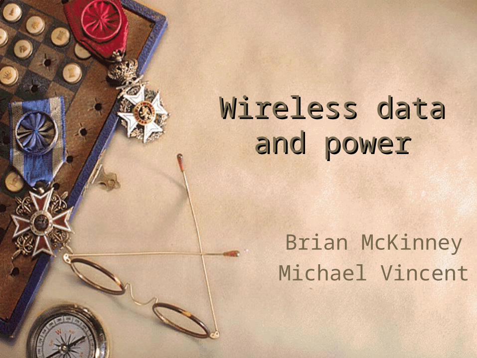
Test Bench
Not a mixed signal IC but needed for simulation and testing purposes
Generates random data Frames random data (e.g. start/stop and parity
bits) Modulates carrier (ASK) with framed data

Regulator
“Buck” type step down switching regulator

Ramp Generator
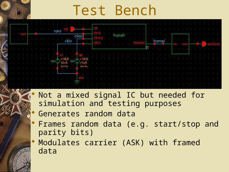
Comparator
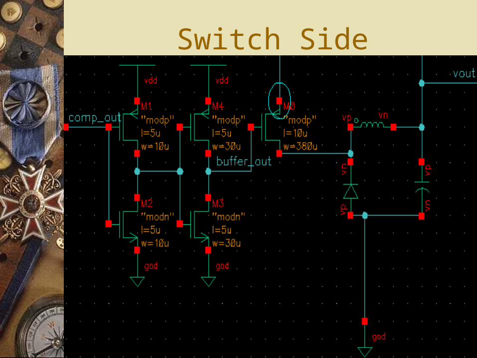
Switch Side
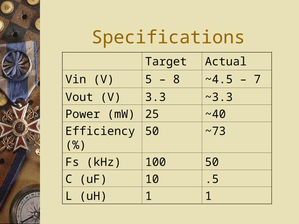
SpecificationsTarget Actual
Vin (V) 5 – 8 ~4.5 – 7
Vout (V) 3.3 ~3.3
Power (mW) 25 ~40
Efficiency (%) 50 ~73
Fs (kHz) 100 50
C (uF) 10 .5
L (uH) 1 1
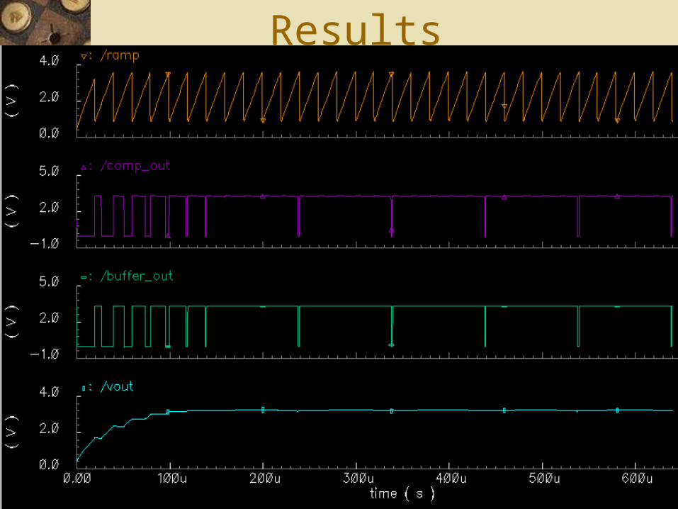
Results
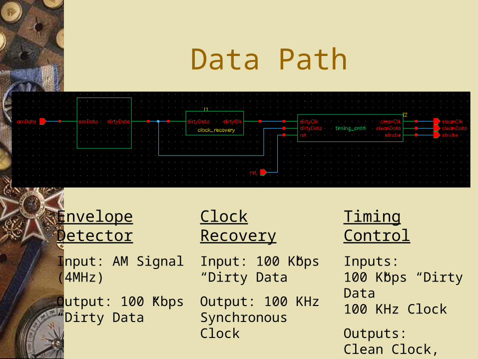
Data Path
Envelope Detector
Input: AM Signal (4MHz)
Output: 100 Kbps “Dirty Data”
Clock Recovery
Input: 100 Kbps “Dirty Data”
Output: 100 KHz Synchronous Clock
Timing Control
Inputs: 100 Kbps “Dirty Data”100 KHz Clock
Outputs: Clean Clock, Clean Data, Frame Strobe

Behavioral Simulation

Bandpass Filter
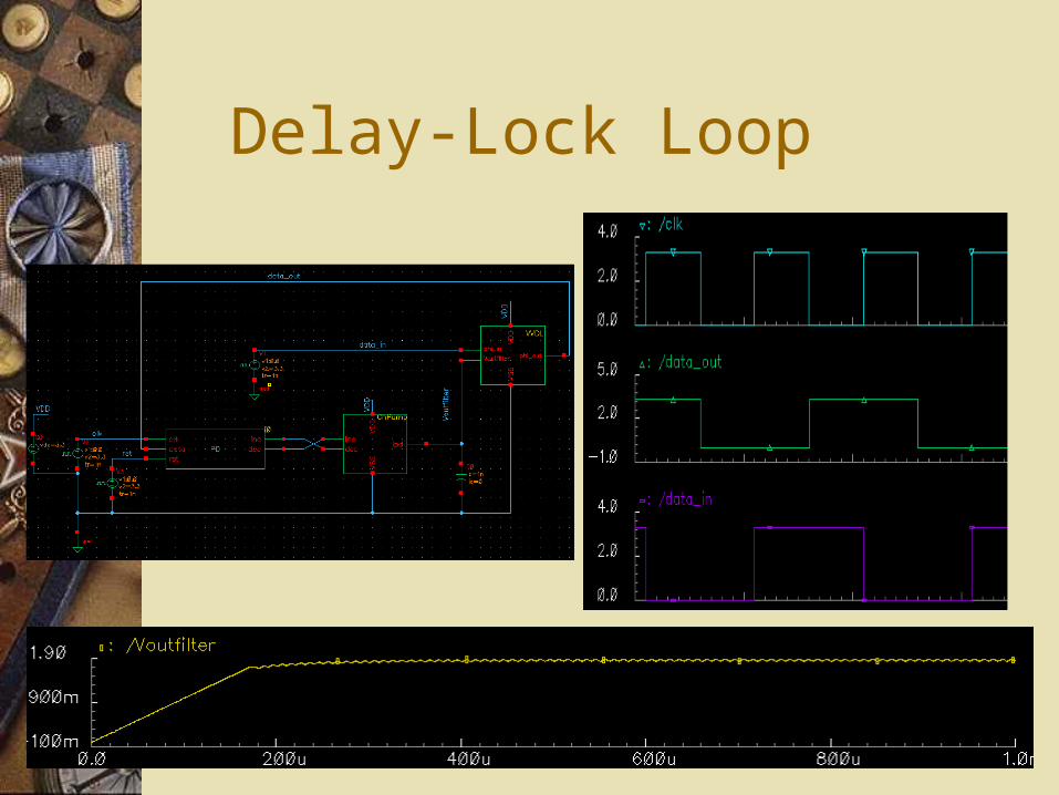
Delay-Lock Loop

PLL Theory
FVCOPD
FVCOPD
data
clk
KKKs
KKKsH
)(
Vsrad
VDD
ffK
sRCK
VDDK
VCO
F
PD
319,8
1
1
radV 1.0504
minmax
RCKK
RCs
s
RCKK
sHVCOPD
VCOPD
data
clk
2
)(
65.02
1
2.12
n
nL
VCOPDn
RC
msTRCN
KK
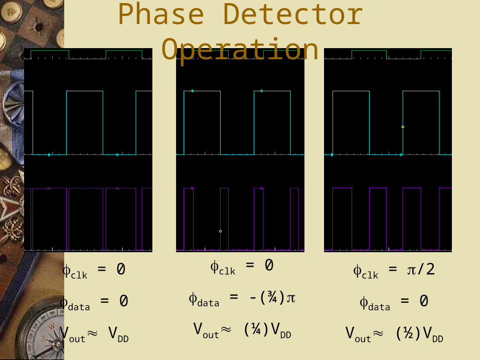
Phase Detector Operation
clk = 0
data = 0
Vout VDD
clk = 0
data = -(¾)
Vout (¼)VDD
clk = /2
data = 0
Vout (½)VDD
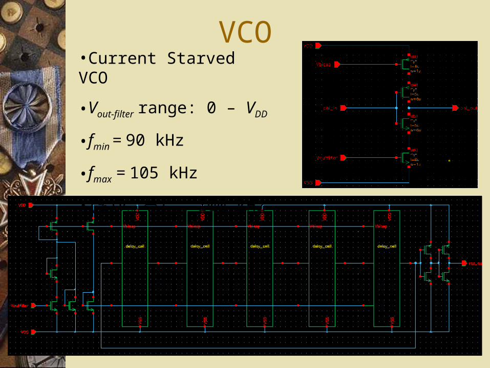
VCO•Current Starved VCO
•Vout-filter range: 0 – VDD
•fmin = 90 kHz
•fmax = 105 kHz
•(½)VDD ftyp = 100 kHz
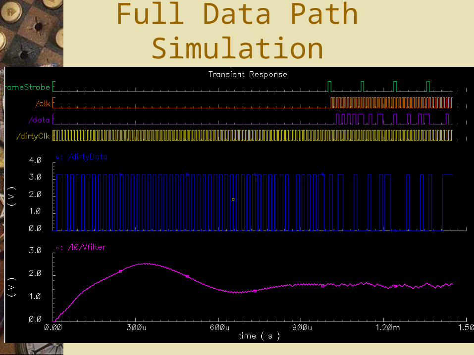
Full Data Path Simulation

Conclusions and Q&A