Embed Size (px)
Citation preview

Wire Bonding IssuesAlan Honma, CERN PH-DT
◆ The CERN bond lab ◆ 5 Selected problems ◆ The ATLAS IBL repair (problem #6) ◆ Conclusion
14 October 2015 UK Wire Bonders Forum

14 October 2015 A. Honma, UK Wire Bonders Forum 2
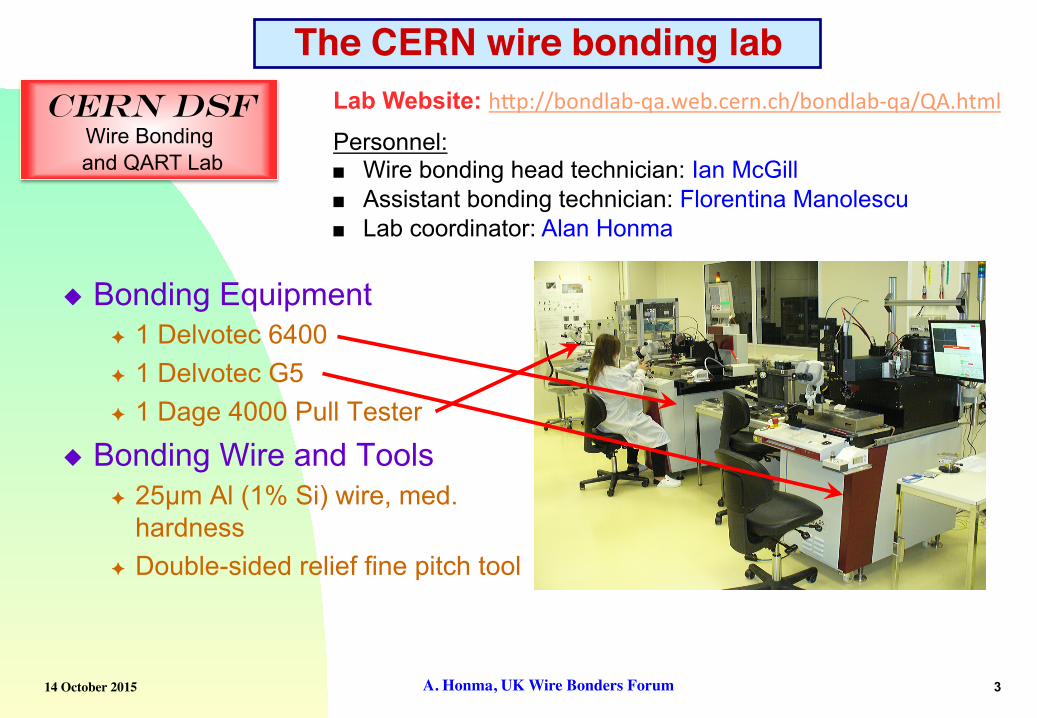
The CERN wire bonding lab
CERN DSF Wire Bonding
and QART Lab
The PH Departmental Silicon Facility (DSF)
Bonding lab
Quality Assurance and Reliability Testing (QART) lab
Shared Clean Room Facilities
Rad det
RD
50
Air Treatment Plant Room
Bonding and
QART
QA
RT Shared DSF Clean Room
ALICE, LHCb, CMS, QART
QART
Bonding and QART Lab Clean Room
Located in B186 ground floor:
14 October 2015 A. Honma, UK Wire Bonders Forum 3
◆ Bonding Equipment ✦ 1 Delvotec 6400 ✦ 1 Delvotec G5 ✦ 1 Dage 4000 Pull Tester
◆ Bonding Wire and Tools ✦ 25µm Al (1% Si) wire, med.
hardness ✦ Double-sided relief fine pitch tool
The CERN wire bonding labCERN DSF
Wire Bonding and QART Lab
Lab Website: h"p://bondlab-‐qa.web.cern.ch/bondlab-‐qa/QA.html
Personnel: ■ Wire bonding head technician: Ian McGill ■ Assistant bonding technician: Florentina Manolescu ■ Lab coordinator: Alan Honma
14 October 2015 A. Honma, UK Wire Bonders Forum 4
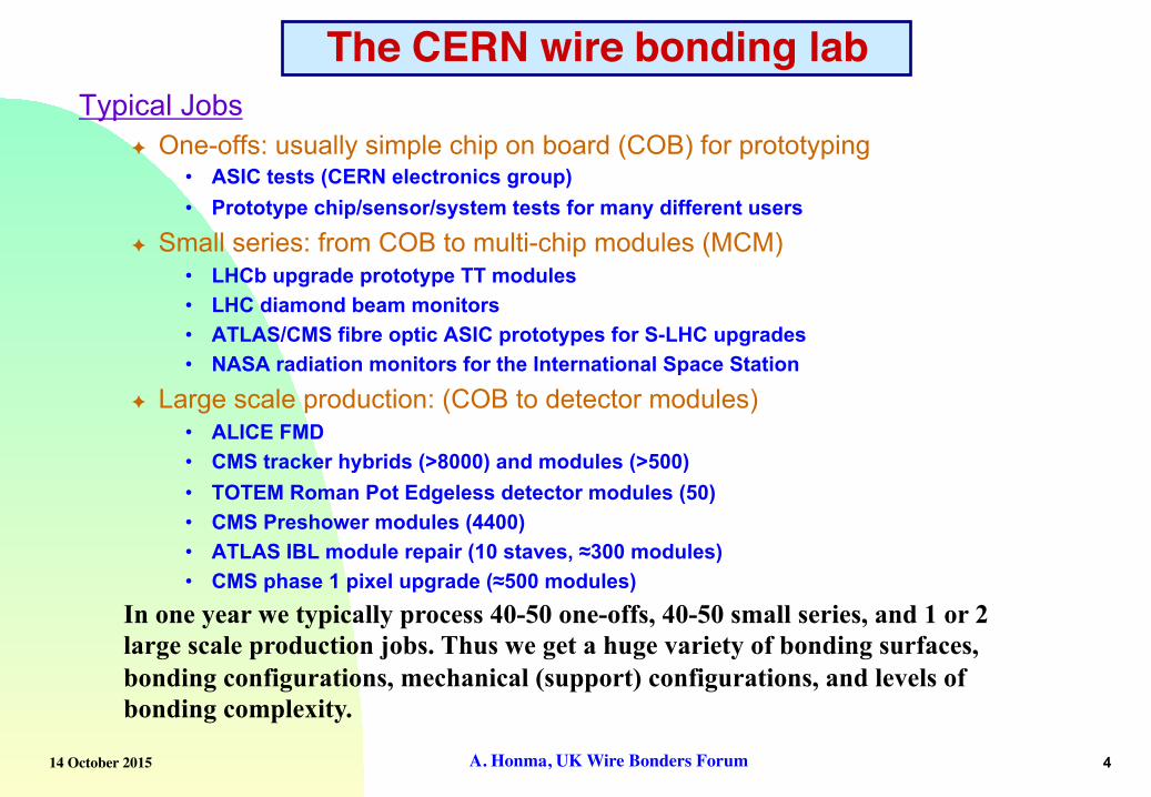
Typical Jobs ✦ One-offs: usually simple chip on board (COB) for prototyping
• ASIC tests (CERN electronics group) • Prototype chip/sensor/system tests for many different users
✦ Small series: from COB to multi-chip modules (MCM) • LHCb upgrade prototype TT modules • LHC diamond beam monitors • ATLAS/CMS fibre optic ASIC prototypes for S-LHC upgrades • NASA radiation monitors for the International Space Station
✦ Large scale production: (COB to detector modules) • ALICE FMD • CMS tracker hybrids (>8000) and modules (>500) • TOTEM Roman Pot Edgeless detector modules (50) • CMS Preshower modules (4400) • ATLAS IBL module repair (10 staves, ≈300 modules) • CMS phase 1 pixel upgrade (≈500 modules)
The CERN wire bonding lab
In one year we typically process 40-50 one-offs, 40-50 small series, and 1 or 2 large scale production jobs. Thus we get a huge variety of bonding surfaces, bonding configurations, mechanical (support) configurations, and levels of bonding complexity.
14 October 2015 A. Honma, UK Wire Bonders Forum 5
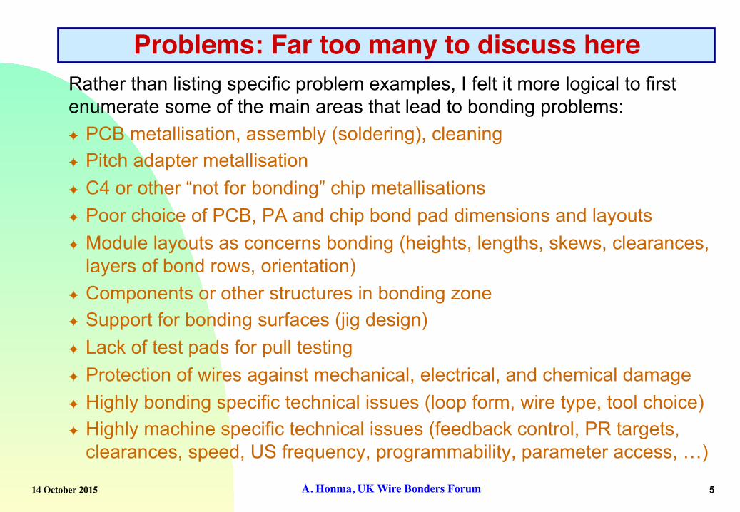
Rather than listing specific problem examples, I felt it more logical to first enumerate some of the main areas that lead to bonding problems: ✦ PCB metallisation, assembly (soldering), cleaning ✦ Pitch adapter metallisation ✦ C4 or other “not for bonding” chip metallisations ✦ Poor choice of PCB, PA and chip bond pad dimensions and layouts ✦ Module layouts as concerns bonding (heights, lengths, skews, clearances,
layers of bond rows, orientation) ✦ Components or other structures in bonding zone ✦ Support for bonding surfaces (jig design) ✦ Lack of test pads for pull testing ✦ Protection of wires against mechanical, electrical, and chemical damage ✦ Highly bonding specific technical issues (loop form, wire type, tool choice) ✦ Highly machine specific technical issues (feedback control, PR targets,
clearances, speed, US frequency, programmability, parameter access, …)
Problems: Far too many to discuss here
14 October 2015 A. Honma, UK Wire Bonders Forum 6
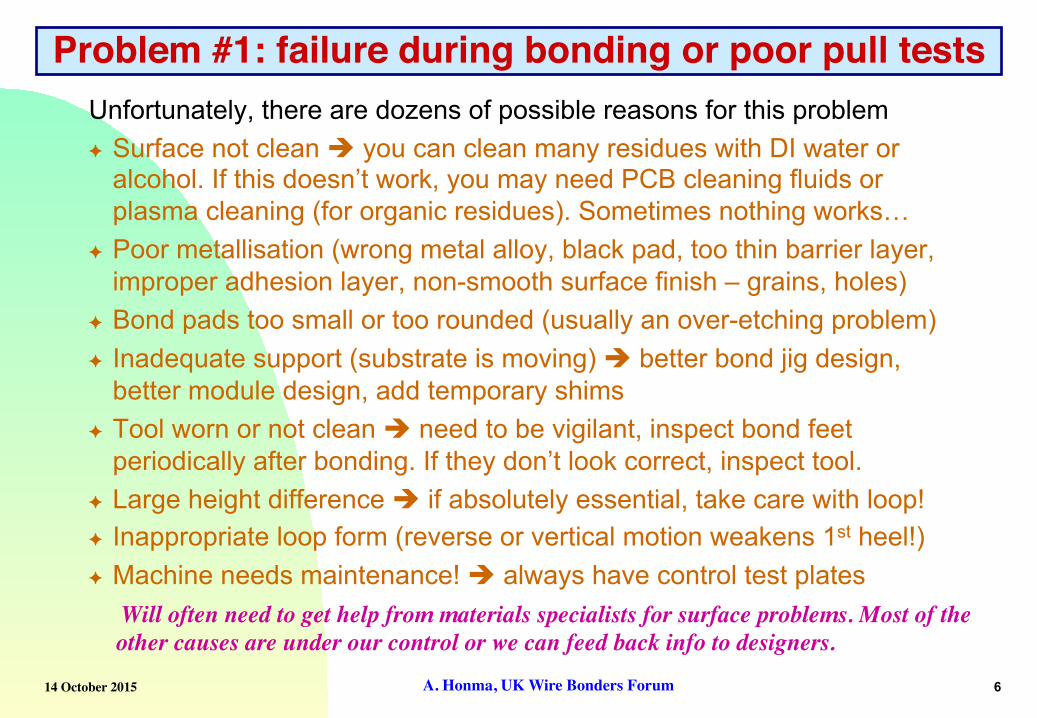
Unfortunately, there are dozens of possible reasons for this problem ✦ Surface not clean è you can clean many residues with DI water or
alcohol. If this doesn’t work, you may need PCB cleaning fluids or plasma cleaning (for organic residues). Sometimes nothing works…
✦ Poor metallisation (wrong metal alloy, black pad, too thin barrier layer, improper adhesion layer, non-smooth surface finish – grains, holes)
✦ Bond pads too small or too rounded (usually an over-etching problem) ✦ Inadequate support (substrate is moving) è better bond jig design,
better module design, add temporary shims ✦ Tool worn or not clean è need to be vigilant, inspect bond feet
periodically after bonding. If they don’t look correct, inspect tool. ✦ Large height difference è if absolutely essential, take care with loop! ✦ Inappropriate loop form (reverse or vertical motion weakens 1st heel!) ✦ Machine needs maintenance! è always have control test plates
Problem #1: failure during bonding or poor pull tests
Will often need to get help from materials specialists for surface problems. Most of the other causes are under our control or we can feed back info to designers.
14 October 2015 A. Honma, UK Wire Bonders Forum 7
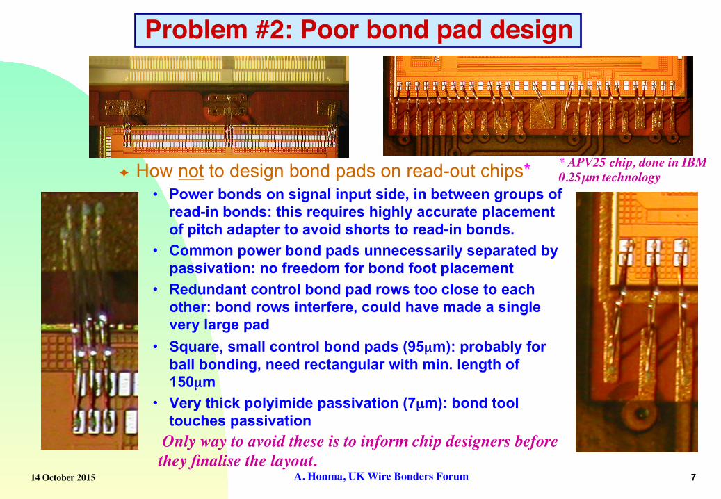
✦ How not to design bond pads on read-out chips* • Power bonds on signal input side, in between groups of
read-in bonds: this requires highly accurate placement of pitch adapter to avoid shorts to read-in bonds.
• Common power bond pads unnecessarily separated by passivation: no freedom for bond foot placement
• Redundant control bond pad rows too close to each other: bond rows interfere, could have made a single very large pad
• Square, small control bond pads (95µm): probably for ball bonding, need rectangular with min. length of 150µm
• Very thick polyimide passivation (7µm): bond tool touches passivation
Problem #2: Poor bond pad design
* APV25 chip, done in IBM 0.25µm technology
Only way to avoid these is to inform chip designers before they finalise the layout.
14 October 2015 A. Honma, UK Wire Bonders Forum 8
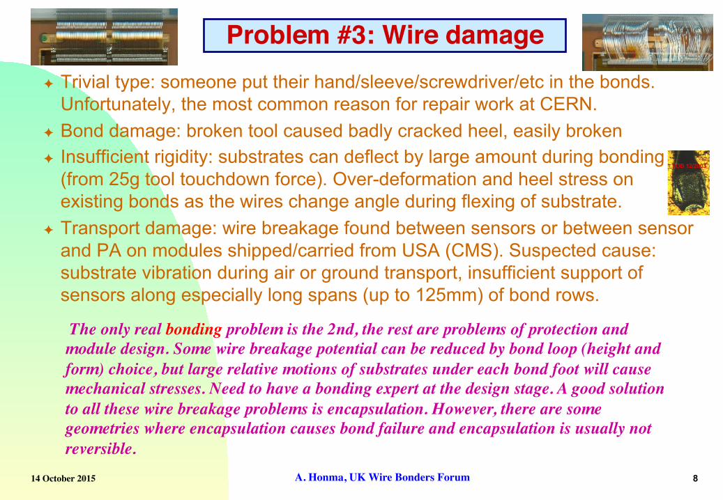
✦ Trivial type: someone put their hand/sleeve/screwdriver/etc in the bonds. Unfortunately, the most common reason for repair work at CERN.
✦ Bond damage: broken tool caused badly cracked heel, easily broken ✦ Insufficient rigidity: substrates can deflect by large amount during bonding
(from 25g tool touchdown force). Over-deformation and heel stress on existing bonds as the wires change angle during flexing of substrate.
✦ Transport damage: wire breakage found between sensors or between sensor and PA on modules shipped/carried from USA (CMS). Suspected cause: substrate vibration during air or ground transport, insufficient support of sensors along especially long spans (up to 125mm) of bond rows.
Problem #3: Wire damage
The only real bonding problem is the 2nd, the rest are problems of protection and module design. Some wire breakage potential can be reduced by bond loop (height and form) choice, but large relative motions of substrates under each bond foot will cause mechanical stresses. Need to have a bonding expert at the design stage. A good solution to all these wire breakage problems is encapsulation. However, there are some geometries where encapsulation causes bond failure and encapsulation is usually not reversible.
14 October 2015 A. Honma, UK Wire Bonders Forum 9
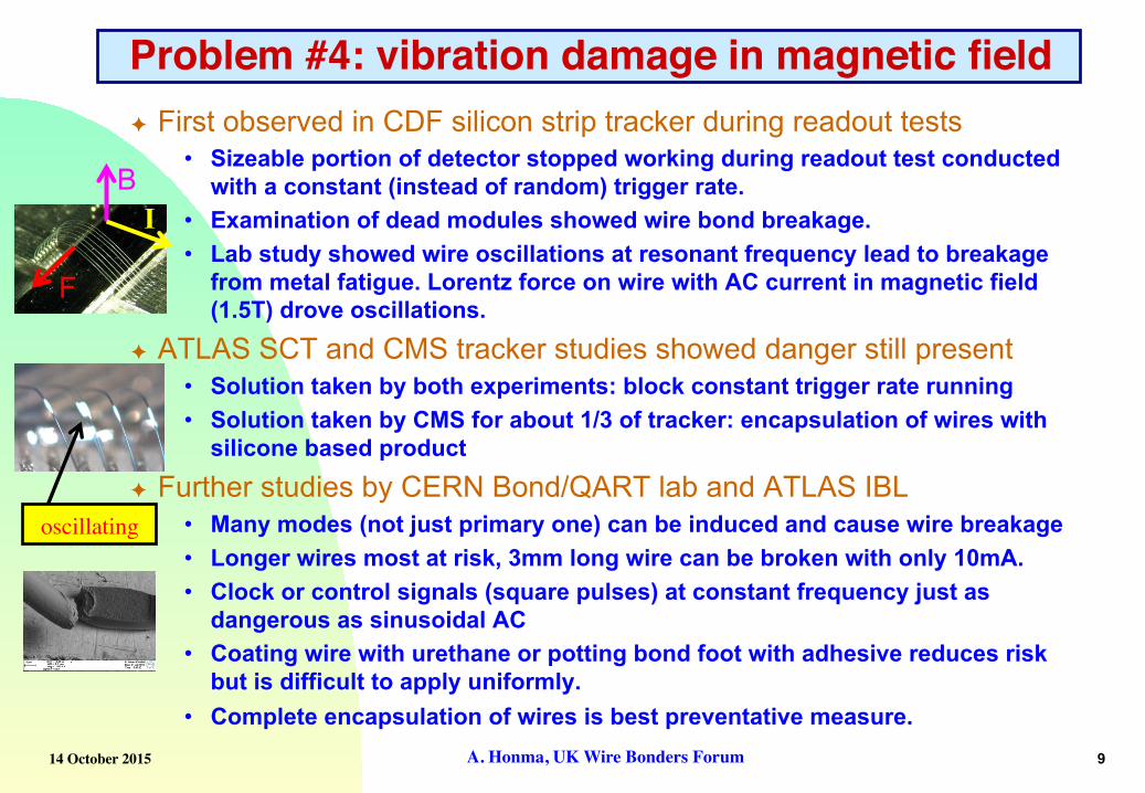
✦ First observed in CDF silicon strip tracker during readout tests • Sizeable portion of detector stopped working during readout test conducted
with a constant (instead of random) trigger rate. • Examination of dead modules showed wire bond breakage. • Lab study showed wire oscillations at resonant frequency lead to breakage
from metal fatigue. Lorentz force on wire with AC current in magnetic field (1.5T) drove oscillations.
✦ ATLAS SCT and CMS tracker studies showed danger still present • Solution taken by both experiments: block constant trigger rate running • Solution taken by CMS for about 1/3 of tracker: encapsulation of wires with
silicone based product ✦ Further studies by CERN Bond/QART lab and ATLAS IBL
• Many modes (not just primary one) can be induced and cause wire breakage • Longer wires most at risk, 3mm long wire can be broken with only 10mA. • Clock or control signals (square pulses) at constant frequency just as
dangerous as sinusoidal AC • Coating wire with urethane or potting bond foot with adhesive reduces risk
but is difficult to apply uniformly. • Complete encapsulation of wires is best preventative measure.
Problem #4: vibration damage in magnetic field
B I
F
oscillating
14 October 2015 A. Honma, UK Wire Bonders Forum 10
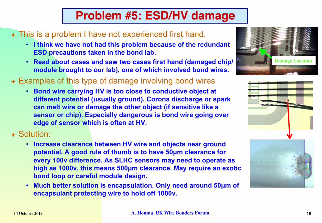
✦ This is a problem I have not experienced first hand. • I think we have not had this problem because of the redundant
ESD precautions taken in the bond lab. • Read about cases and saw two cases first hand (damaged chip/
module brought to our lab), one of which involved bond wires. ✦ Examples of this type of damage involving bond wires
• Bond wire carrying HV is too close to conductive object at different potential (usually ground). Corona discharge or spark can melt wire or damage the other object (if sensitive like a sensor or chip). Especially dangerous is bond wire going over edge of sensor which is often at HV.
✦ Solution: • Increase clearance between HV wire and objects near ground
potential. A good rule of thumb is to have 50µm clearance for every 100v difference. As SLHC sensors may need to operate as high as 1000v, this means 500µm clearance. May require an exotic bond loop or careful module design.
• Much better solution is encapsulation. Only need around 50µm of encapsulant protecting wire to hold off 1000v.
Problem #5: ESD/HV damage
Damage Location
14 October 2015 A. Honma, UK Wire Bonders Forum 11
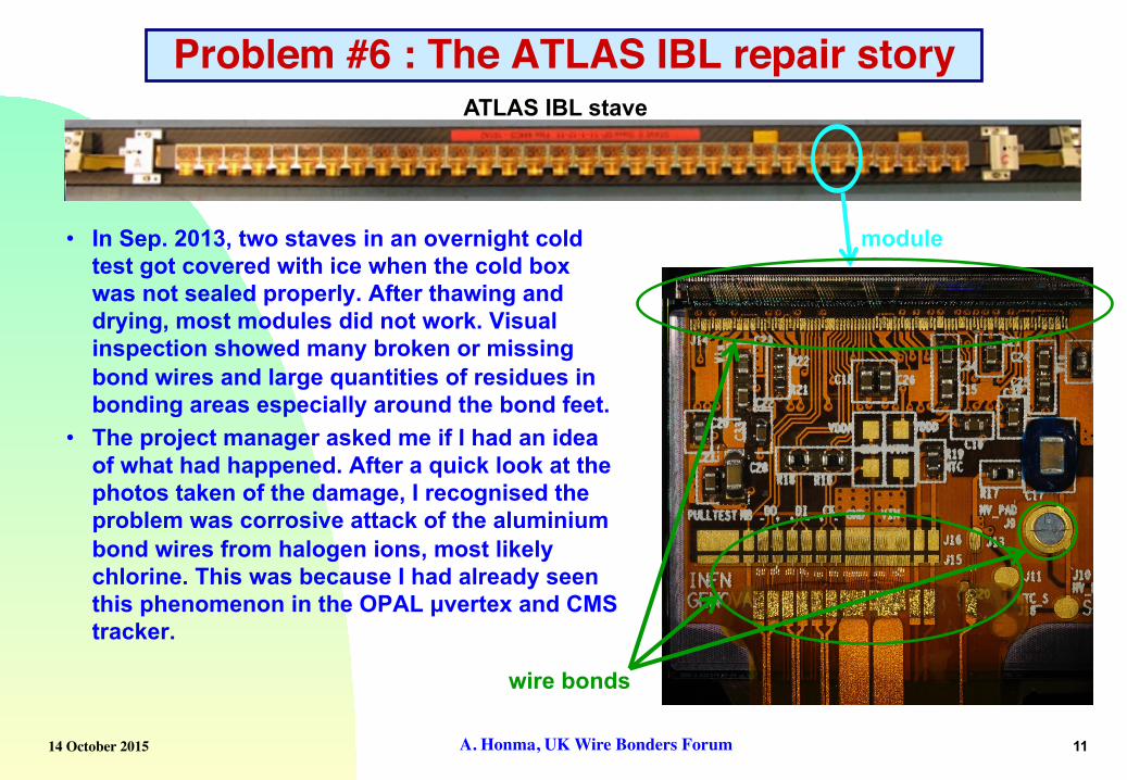
• In Sep. 2013, two staves in an overnight cold test got covered with ice when the cold box was not sealed properly. After thawing and drying, most modules did not work. Visual inspection showed many broken or missing bond wires and large quantities of residues in bonding areas especially around the bond feet.
• The project manager asked me if I had an idea of what had happened. After a quick look at the photos taken of the damage, I recognised the problem was corrosive attack of the aluminium bond wires from halogen ions, most likely chlorine. This was because I had already seen this phenomenon in the OPAL µvertex and CMS tracker.
Problem #6 : The ATLAS IBL repair storyATLAS IBL stave
module
wire bonds
14 October 2015 A. Honma, UK Wire Bonders Forum 12
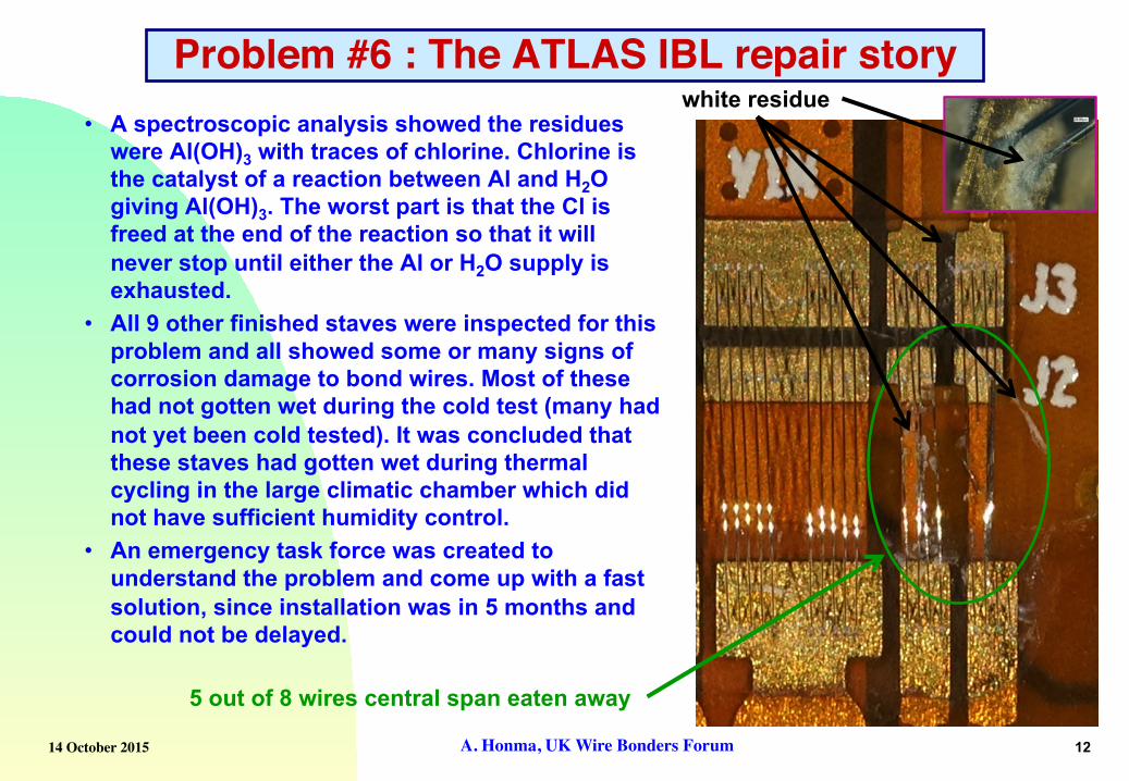
• A spectroscopic analysis showed the residues were Al(OH)3 with traces of chlorine. Chlorine is the catalyst of a reaction between Al and H2O giving Al(OH)3. The worst part is that the Cl is freed at the end of the reaction so that it will never stop until either the Al or H2O supply is exhausted.
• All 9 other finished staves were inspected for this problem and all showed some or many signs of corrosion damage to bond wires. Most of these had not gotten wet during the cold test (many had not yet been cold tested). It was concluded that these staves had gotten wet during thermal cycling in the large climatic chamber which did not have sufficient humidity control.
• An emergency task force was created to understand the problem and come up with a fast solution, since installation was in 5 months and could not be delayed.
Problem #6 : The ATLAS IBL repair story
5 out of 8 wires central span eaten away
white residue
14 October 2015 A. Honma, UK Wire Bonders Forum 13
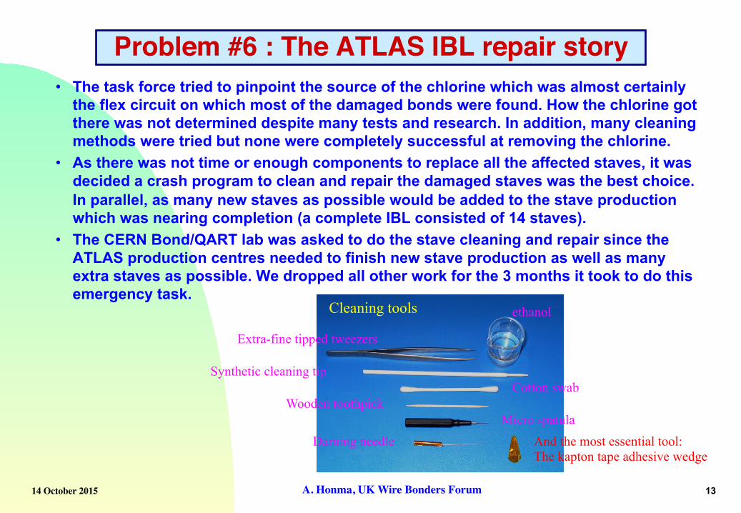
• The task force tried to pinpoint the source of the chlorine which was almost certainly the flex circuit on which most of the damaged bonds were found. How the chlorine got there was not determined despite many tests and research. In addition, many cleaning methods were tried but none were completely successful at removing the chlorine.
• As there was not time or enough components to replace all the affected staves, it was decided a crash program to clean and repair the damaged staves was the best choice. In parallel, as many new staves as possible would be added to the stave production which was nearing completion (a complete IBL consisted of 14 staves).
• The CERN Bond/QART lab was asked to do the stave cleaning and repair since the ATLAS production centres needed to finish new stave production as well as many extra staves as possible. We dropped all other work for the 3 months it took to do this emergency task.
Problem #6 : The ATLAS IBL repair story
Cleaning tools
ethanol
Extra-fine tipped tweezers
Synthetic cleaning tip Cotton swab
Wooden toothpick Micro spatula
Darning needle And the most essential tool: The kapton tape adhesive wedge
14 October 2015 A. Honma, UK Wire Bonders Forum 14
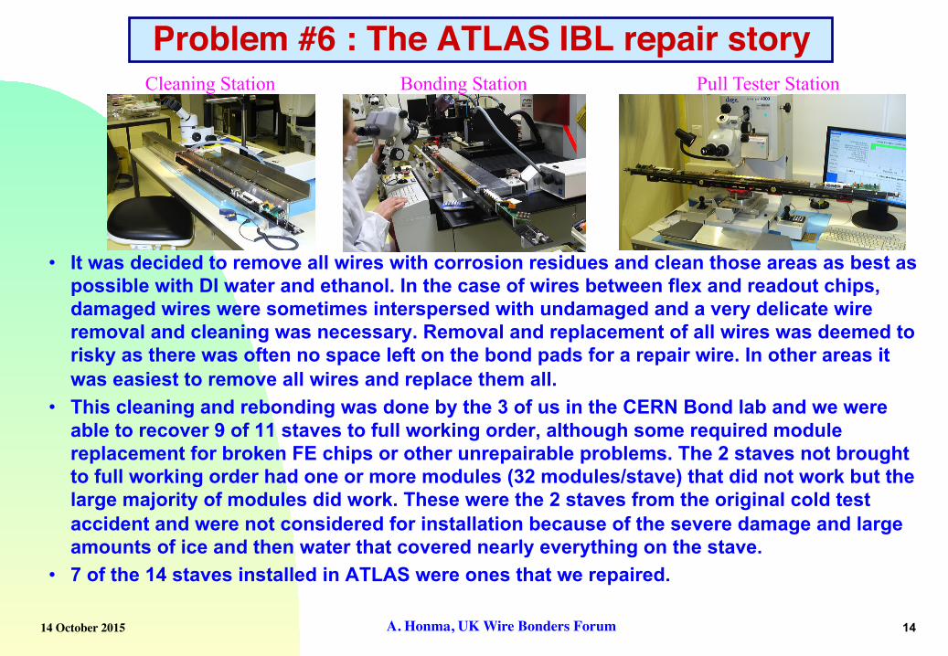
• It was decided to remove all wires with corrosion residues and clean those areas as best as possible with DI water and ethanol. In the case of wires between flex and readout chips, damaged wires were sometimes interspersed with undamaged and a very delicate wire removal and cleaning was necessary. Removal and replacement of all wires was deemed to risky as there was often no space left on the bond pads for a repair wire. In other areas it was easiest to remove all wires and replace them all.
• This cleaning and rebonding was done by the 3 of us in the CERN Bond lab and we were able to recover 9 of 11 staves to full working order, although some required module replacement for broken FE chips or other unrepairable problems. The 2 staves not brought to full working order had one or more modules (32 modules/stave) that did not work but the large majority of modules did work. These were the 2 staves from the original cold test accident and were not considered for installation because of the severe damage and large amounts of ice and then water that covered nearly everything on the stave.
• 7 of the 14 staves installed in ATLAS were ones that we repaired.
Problem #6 : The ATLAS IBL repair storyCleaning Station Bonding Station Pull Tester Station
14 October 2015 A. Honma, UK Wire Bonders Forum 15
• In parallel to the repair work, studies were made of coating the wires with urethane or potting the bond feet with an adhesive material used in the outer ATLAS pixel detector. It was decided not to try to coat or pot because these methods could not get the extensive testing (mostly irradiation tests) needed to check if they were both safe and effective.
• Note that the coating and potting studies were also done to try to protect the wires from potential vibration damage in the magnetic field as described in “Problem #4”.
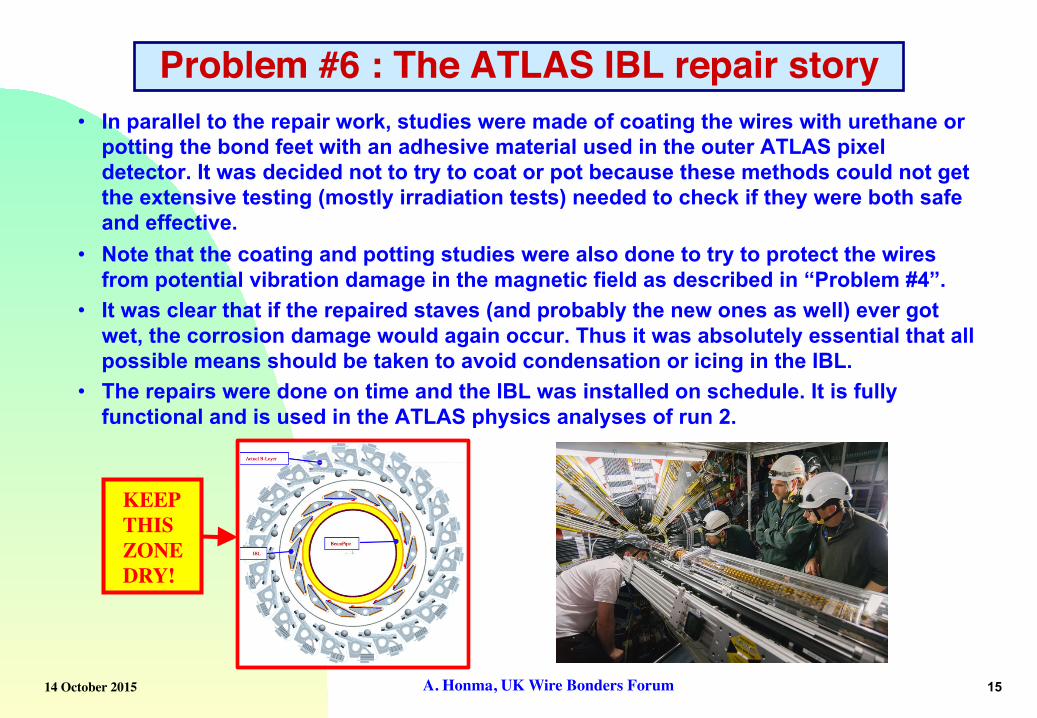
• It was clear that if the repaired staves (and probably the new ones as well) ever got wet, the corrosion damage would again occur. Thus it was absolutely essential that all possible means should be taken to avoid condensation or icing in the IBL.
• The repairs were done on time and the IBL was installed on schedule. It is fully functional and is used in the ATLAS physics analyses of run 2.
Problem #6 : The ATLAS IBL repair story
KEEP THIS ZONE DRY!
14 October 2015 A. Honma, UK Wire Bonders Forum 16
Conclusions✦ I have given 6 examples of bonding problems we have encountered, but
the list is long. To name a few other important ones we have experienced: • whiskering • cratering • dendrite growth (on bond pads) • touching wires • overcurrent (fusing)
✦ Workshops like this are a good means of sharing experience • Avoid making the same mistake • Get insight from others on solutions to difficult bonding situations • Move away from the “us versus them” attitude. Our detectors are very costly, we
can ill afford to have a major failure – it hurts us all. ✦ The CERN Bond/QART lab is in service to our field:
• Please feel free to ask for advice (especially of Ian for technical questions!) • We are happy to have visits and technical discussions • We try to be a “repository” for bonding information, all input is welcome