Embed Size (px)
Citation preview

ISSN 1064�2269, Journal of Communications Technology and Electronics, 2016, Vol. 61, No. 6, pp. 551–573. © Pleiades Publishing, Inc., 2016.Original Russian Text © V.Yu. Shishkov, A.A. Zyablovskii, E.S. Andrianov, A.A. Pukhov, A.P. Vinogradov, A.V. Dorofeenko, S.A. Nikitov, A.A. Lisyanskii, 2016, publishedin Radiotekhnika i Elektronika, 2016, Vol. 61, No. 6, pp. 509–533.
551
INTRODUCTION
The development of communication technologiesnecessitates the construction of devices for conversionof electrical signals into optical signals for the trans�mission in optical communication channels. The fol�lowing requirements must be satisfied for such devices:relatively high modulation frequency of signals, lowgeneration threshold, narrow directional pattern ofoutput signal, and low production costs. Lasers withcavities based on a defect mode in photonic crystal(vertical�cavity surface emitting (VCSE) lasers) [1–4]and distributed�feedback (DFB) lasers are used atpresent for such purposes. Sources of coherent radia�tion based on composite materials containing plasmonnanostructures [5–11] may serve as alternativesources. The modulation frequency that is higher thanthat of the VCSE and DFB lasers is the main advantageof the alternative sources.
Normally, a VCSE laser consists of two 1D photo�
nic crystals1 (Bragg mirrors) with a resonant cavity in
between [12–20] and amplifying medium that isplaced in the resonant cavity. The laser generation insuch devices takes place along the direction that is per�pendicular to the layer plane.
The amplifying medium in a VCSE laser representsa thin layer of a narrow�band�gap semiconductor thatis placed between two layers of a wide�band�gap semi�conductor. Such a heterostructure works as a quantumwell when the amplifying layer is relatively thin [12].The total energy of carriers in quantum wells is a sumof discrete levels that emerge owing to the space quan�tization along the direction that is perpendicular to the
1 See Appendix 1 for the properties of photonic crystals.
layer and a continuous component that describes themotion along the layer:
(1)
where p are the momenta of carrier along the layer, mis the effective mass of carrier, l is the layer thickness,and n is the integer.
Radiative transitions of electron from the conduc�tion band to the valence band serve as working levels inquantum wells. The photon frequency in quantumwells is a sum of the band gap of bulk semiconductorand a discrete quantity related to the finite thickness ofthe semiconductor film. The dependence of the tran�sition frequency on the film thickness can be used toaccurately tune the transition frequency to the cavitymode [12].
When the thickness of the resonant cavity is onehalf of the wavelength of the generated radiation, thesingle�mode lasing is easily reached in VCSE lasers[17, 21]. The VCSE laser can be stabilized with respectto thermal fluctuations owing to a relatively high Qfactor of the vertical cavity. The amplification band is
highly sensitive to the thermal fluctuations [15].2 If the
2 Temperature variations lead to variations in the thickness of lay�ers in the VCSE�laser structure, so that the mode frequency ofthe cavity and frequency of amplification band are varied. Thefrequency of cavity mode is inversely proportional to the layerthickness, and the frequency of the amplification band isinversely proportional to the squared thickness owing to spacequantization of the energy of carriers. Therefore, the frequencyof the amplification band is significantly more sensitive to varia�tions in temperature in comparison with the frequency of thecavity mode.
π= +
�tot
2 2 22
2,
2 2
pE n
m ml
Wide�Aperture Planar LasersV. Yu. Shishkova, b, A. A. Zyablovskiia, b, E. S. Andrianova, b, A. A. Pukhova, b, c, A. P. Vinogradova, b, c,
A. V. Dorofeenkoa, b, c, S. A. Nikitova, d, and A. A. Lisyanskiie, f
aDukhov All�Russia Research Institute of Automatics, Sushchevskaya ul. 22, Moscow, 127055 RussiabMoscow Institute of Physics and Technology (State University), Institutskii per. 9, Dolgoprudnyi, Moscow oblast, 141700 Russia
cInstitute for Theoretical and Applied Electrodynamics, Russian Academy of Sciences, Izhorskaya ul. 13, Moscow, 125412 Russia
dKotel’nikov Institute of Radio Engineering and Electronics, Russian Academy of Sciences, Mokhovaya ul. 11, str. 7, Moscow, 125009 Russia
eQueens College, The City University of New York, 65�30 Kissena Blvd., Queens, NY 11367�1597 USAfThe Graduate Center, The City University of New York, 365 Fifth Avenue, New York, NY 10016 USA
e�mail: [email protected] January 27, 2015
Abstract—Wide�aperture planar lasers (vertical�cavity surface emitting lasers, distributed feedback lasers,2D spaser arrays, and plasmon lasers on stopped�light mode) are reviewed. Structure, parameters (directionalpattern and amplitude modulation frequency), and physical principles of such lasers are discussed.
DOI: 10.1134/S1064226916050107
REVIEW
552
JOURNAL OF COMMUNICATIONS TECHNOLOGY AND ELECTRONICS Vol. 61 No. 6 2016
SHISHKOV et al.
amplification band is significantly broader than thecavity band, the latter determines the laser frequency(frequency pulling) [12, 22, 23]. Such a frequency sta�bility is an advantage of vertical�cavity lasers in opto�electronic applications in which the laser frequencymust be tuned to the waveguide mode of optical fiber.
A DFB laser may serve as an alternative to a VCSElaser. In the DFB lasers, the laser mode is generatedowing to multiple scattering by periodic photonic�crystal structure rather than reflection from cavitymirrors.
The DFB lasers that are employed in optoelectron�ics contain plates of 2D photonic crystal (PC) inwhich amplifying medium is used as a matrix [24]. Thewave vector of the laser mode in such systems belongsto the plate plane and the generated radiation is emit�
ted along the perpendicular direction.3 The emission
from the PC surface takes place due to the fact that thespatial spectrum of the Bloch wave contains wavenumbers the tangential components of which are lessthan the wave number in surrounding space. Thewidth of the directional pattern of the emitter is deter�mined by the size of the emitting aperture, in particu�lar, the transverse size of the PC plate. Therefore, thesize of the PC plate must be significantly greater than
the wavelength.4 An increase in the PC size leads to a
decrease in loss related to the emission from the endsurfaces of the plate and, hence, a decrease in the las�ing threshold.
Note the nonlinearity of the regime of developedgeneration. In this case, the permittivity of the activematrix depends on the field intensity and is modulatedwith the period of the Bloch wave. In general, theperiod of the Bloch wave is incommensurable with thePC period and the development of lasing causes dis�tortions of the PC periodicity. Thus, the mode ceasesto be the mode of the Bloch wave, the scattering bysingle cells looses long�range order, and the direc�tional pattern becomes broader. In the exceptionalcase, the lasing in the DFB laser takes place at fre�quencies in the vicinity of the boundary of the PCband gap, so that the period of the Bloch wave almostcoincides with the PC period and the modulation ofthe active medium caused by the generated wave doesnot lead to violations of the PC periodicity.
The closeness of the laser frequency to the edge ofthe band gap determines the physical scenario of las�ing. Owing to the Bragg reflection, the Bloch wave atthe edge of the band gap is transformed into a standingwave, so that the conditions for the cavityless lasing aresatisfied. This circumstance accounts for the term dis�tributed�feedback lasers.
3 In the first DFB lasers, the radiation was emitted along thedirection of generation. However, such a configuration cannotbe used to construct a radiation source with a relatively narrowdirectional pattern.
4 A narrow beam is needed for efficient delivery of the optical sig�nal of the DFB laser to optical fiber.
Thus, the modes at the boundary of the PC bandgap exhibit the lowest lasing threshold, the radiation ofsuch modes is emitted along the direction that isorthogonal to the plane of the PC plate, and the devel�opment of lasing at frequencies in the vicinity of theboundary of the PC band gap does not destroy the PCperiodicity.
1. SIMPLIFIED MODEL OF DFB LASER
To illustrate the above analysis, we consider a DFBlaser (Fig. 1). We assume that the plate made of theamplifying medium is placed in lossless medium withpermittivity εlm.
To describe the interaction of electromagnetic fieldand amplifying medium, we use the system of theMaxwell–Bloch equations [25] that is represented inthe following way for the propagation along the direc�tion that is perpendicular to layers [25, 26]:
(2)
(3)
(4)
Here, E is the electric field, P is the polarization, n isthe population inversion of the gain medium, is thepopulation inversion that is reached in the medium inthe absence of electromagnetic field, ωQD is the transi�
tion frequency of quantum dots (QDs), is thesquare of the dipole moment of the transition in thegain medium, and τp and τinv are the characteristicrelaxation times of polarization and population inver�sion. The system of the Maxwell–Bloch equations wasderived in [25] on the assumption that the amplifyingmedium represents an ensemble of two�level systemsthe population inversion in which results from externalaction. The two�level systems were described using thequantum�mechanical equations for the density matrixthat are reduced to equations for polarization P andpopulation inversion n. The electromagnetic field inthe system was analyzed on the assumption that quan�tum fluctuations can be disregarded owing to a rela�tively large number of photons in the system and thatthe field can be described with the aid of classicalMaxwell equations. The field amplification resultsfrom the stimulated transitions in the amplifyingmedium, and the energy transition from the amplify�ing medium to the electromagnetic wave is describedusing a term on the right�hand side of Eq. (2). Such anapproximation is known as the semiclassical approxi�mation [25].
( )2 2 2
2 2 2 2 24 ,
xE E Px c t c t
ε∂ ∂ π∂− =
∂ ∂ ∂
ω∂ ∂+ + ω = −τ ∂∂
�
�
QDQD
p
22
2
2
22 ,d nEP P P
tt
( )∂ ∂+ − =
∂ τ ω ∂�inv QD0
1 2 .n Pn n Et t
0n
2d�

JOURNAL OF COMMUNICATIONS TECHNOLOGY AND ELECTRONICS Vol. 61 No. 6 2016
WIDE�APERTURE PLANAR LASERS 553
Maxwell–Bloch equations (2)–(4) make it possi�ble to describe the interaction of electromagnetic fieldand amplifying medium. For relatively low fields
= , population inversion is
virtually constant and field�independent. In this case,the field and polarization can be analyzed using linearequations (2)–(4) and the amplifying medium can be
0n n−⎛⎜⎝
∂τ
ω⎞⎟∂ ⎠�
inv
QD0
2 PE nt
�
described with the aid of permittivity with negative fre�quency�dependent imaginary part:
(5)
where εpl is the permittivity of the plate in the absence
of the amplifying medium, α = and β =
( )αω τ
ε ω = ε −
− ω τ + ω − ω
pam p
QD
QD
l
p2 2
2,
2i
π τ
��p
204 ,d n
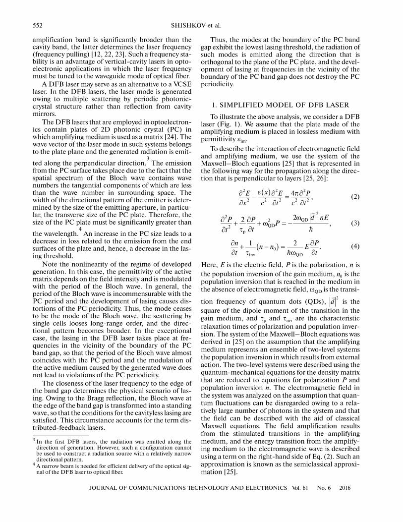
(а)
x
z
y
(b)
x
h
y
(c)
d1 d2
εamδh
εm
ε1 ε2
d1 d2
k1xω
c��� ε1= k2x
ω
c��� ε2=
Fig. 1. (a) Scheme of the DFB laser consisting of an amplifying layer that contains a periodic grating of nanoribbons, (b) schemeof a unit cell of the DFB laser, and (c) a cell of an auxiliary 1D PC with effective permittivities of layers and .1ε 2ε

554
JOURNAL OF COMMUNICATIONS TECHNOLOGY AND ELECTRONICS Vol. 61 No. 6 2016
SHISHKOV et al.
[26, 27], and εam is the permittivity of theamplifying medium that is used to fabricate the PCplate.
A periodic structure of nanoribbons (Fig. 1a) withpermittivity εm is introduced into the film to producethe distributed feedback in the DFB laser. Film thick�ness is h, the distance between nanoribbons is thewidth of nanoribbon is and the height of nanorib�bon is (Fig. 1b). The lower surface of the film lieson the xy plane.
A waveguide mode that is scattered by nanoribbonsmay propagate inside the film. The system under studyis periodic along the x direction, and its single cellconsists of two sections (Fig. 1b). The first section rep�resents a homogeneous dielectric waveguide withthickness h and permittivity εam that is placed intomedium with permittivity εlm. The second section isthe homogeneous (with respect to the x axis) two�layerwaveguide consisting of the layer with thickness with permittivity εam and the layer with thickness and permittivity εm that is placed into medium withpermittivity εlm. Such a system can be analyzed usingan auxiliary 1D PC the single cell of which consists oftwo layers with effective permittivities ε1 and ε2
(Fig. 1c). The effective permittivity and impedance ofthe ith layer (i = 1, 2) can be calculated as =
and = where is the wave vectorof the TE�polarized wave that propagates along the ith
section of the waveguide (Fig. 1b).5
To find quantity , we solve the boundaryeigenvalue problem. The distributions of the electricand magnetic fields in the waveguide (Fig. 1b) aregiven by
(6)
where is the wave number along the waveguideaxis,
5 Such a polarization configuration is chosen with allowance forthe fact that the dipole moments of nanoribbons are induced byelectric field, so that a narrow directional pattern with the maxi�mum along the normal to the PC can be obtained only for theTE polarization.
τ τ
��inv p
2 2d
1,d
2,dhδ
h h− δ
hδ
iε
2 2 2ixc k ω iZ ,iε ( )ixk ω
( )2xk ω
( ) ( )
( ) [ )
+γ
γ −γ
γ − γ
−γ
⎧ ≤⎪
+ ∈ δ⎪= ⎨
+ ∈ δ⎪⎪
≥⎩
lm
mode mode
am am
lm
mode mode
am am
lm
2
2
2
2
, 0,
, 0, ,
, , ,
,
x
x
x
x
ik x z
ik x z z
y ik x i z i z
ik x z
e z
e a e b e z hE
e a e b e z h h
b e z h
,x yH E z= ∂ ∂
2xk
( ) ( )( )
ω ωγ = − ε γ = − ε
ωγ = ε −
lm lm mode mode
am am
2 22 22 2
222
, ,x x
x
k kc c
kc
are the wave numbers along the z axis in the externalmedium, nanoribbon of the auxiliary waveguide, andactive medium of the auxiliary waveguide, respectively.Amplitudes, amode, bmode, aam, bam, and blm are foundfrom the boundary conditions at the edges of layers.With allowance for the boundary conditions, the dis�persion relation for wave vector is written as
(7)
We must assume that δh = 0 in expression (7) tocalculate wave vector at the fragment of thewaveguide outside the nanoribbon. In calculations, weuse parameters εlm, εam, εmode, h, and δh from experi�ments on DFB lasers [9, 28] and obtain
and imaginary parts of ε1 and ε2 that do notdepend on the pump intensity. Below, we study theworking regimes of the DFB laser at different Imε1
and Imε2.The properties of 1D PC are well known (see
Appendix 1). The lasing threshold in PC is determinedby the condition [26, 29]
(8)
where N is the number of PC cells, d is the length ofthe PC cell, r is the reflection coefficient for the PC–vacuum interface, and kB is the Bloch wave numberin the PC. Expression (8) can be divided into ampli�tude and phase conditions for lasing. The amplitudecondition
(9)
Makes it possible to determine the minimum popula�tion inversion n0 that is needed for lasing. Note thatBloch wave vector depends on the permittivityof active layers that, in turn, nonlinearly depends onpopulation inversion n0. In the DFB laser, the reflec�tion from the end surfaces of the plate is insignificant,since the standing mode emerges in the system due tomultiple scattering by the PC periodic structure.Indeed, an increase in the number of the PC cellsalways leads to the scenario in which so thatthe loss related to the emission from the end surfacesof the PC can be neglected. In this case, expression (9)is reduced to equation
(10)
In other words, the lasing threshold for the PC with is determined only by the loss related to emis�
sion along the direction perpendicular to the PC plane
( )2xk ω
( ) ( )( )
( ) ( )( )
( )(
( ))
( ) ( )( )
γ γ γ − δ − γ γ − δ
× γ γ δ + γ γ δ
= γ γ γ − δ
− γ γ − δ
× γ γ δ + γ γ δ
am am am lm am
lm mode mode mode
mode am am
lm am
lm mode mode mode
sinh cosh
cosh sinh
sin ( ) cos ( )
cos ( )
sin ( )
.
h h h h
h h
h h
h h
h h
( )1xk ω
1 ,e 5R 1.ε =
2Re 1.1,ε =
( ) =B2 exp 2 1,r ik Nd
( ) =B 0ln
Im .r
k n dN
( )B 0k n
ln ,N r�
=BIm 0.k
L λ�
JOURNAL OF COMMUNICATIONS TECHNOLOGY AND ELECTRONICS Vol. 61 No. 6 2016
WIDE�APERTURE PLANAR LASERS 555
and the internal loss in the PC�cell material. The con�dition can easily be satisfied at the boundaryof the band gap where the PC impedance is written asZPC ≈ iZPC (see Appendix 1), so that the absolute valueof the reflection coefficient for the PC–insulatorinterface is represented as
Using expression (8), we derive the phase condition
(11)
where n is the integer. Expression (11) makes it possi�ble to determine the radiation frequency of the DFBlaser. It is seen that the lasing takes place when the
phase shift related to a single passage through the sys�tem is a multiple of π.
At frequencies that are close to the second bound�
ary of the band gap, we have = +
where Using formula (11), we obtain
(12)
where Note that m = ±1 for PC modes thatare closest to the band gap.
To find threshold population inversion fromexpression (10), we must determine the dependence ofquantity on the PC parameters with the aidof the Rytov equation [30] (see Appendix 1):
(13)
Threshold parameter is implicitly determinedusing equation
(14)
Expression (14) is an exact expression for the lasingthreshold but, for estimations, we employ the systemof Maxwell–Bloch equations (2)–(4). We assume thatthe lasing in the PC takes place in the vicinity of theQD transition frequency ωQD. Then, electric field Eand polarization P are represented as
where E and P are the real quantities and and are the complex functions the variations in
which are substantially slower than variations in expo�nential function Using such a condition,we represent the Maxwell–Bloch equations as
(15)
(16)
(17)
At the initial stage of lasing, the population inversionis approximately since the field amplitude is insuf�ficient for significant changes of the population inver�sion. In this case, nonlinear system of equations (15)–(17) is reduced to the linear system
(18)
(19)
Thus, slow amplitudes of the field and polarizationcan be represented as
where function satisfies the equation
and, hence, serves as the mode of cavity that repre�sents a finite sample of PC. Finally, we derive the fol�lowing system of equations for variables and :
(20)
(21)
lnN r�
−= ≈
+
PC am
PC am
1.Z Z
rZ Z
( ) ( )ω + = πBRe arg ,k Nd r n
( )ωBRe k 2dπ ( ),kδ ω
( ) 2 .kdπ
δ ω �
( )( )arg
,m r
kL d
π − πδ ω = �
.m n N= −
thr0n
( )ωBIm k
( )
( ) ( ) ( ) ( )⎛ ⎛ ⎛ ⎞ ⎞⎞
− +⎜ ⎜ ⎜ ⎟ ⎟⎟⎝ ⎝ ⎝ ⎠ ⎠⎠ω =
+B
1 21 1 2 2 1 1 2 2
2 1
1 2
1Im arccos cos cos sin sin2
Im .
Z Zk d k d k d k d
Z Zk
d d
thr0n
( ) ( )
( ) ( )
⎛ ⎛⎜ ⎜⎝ ⎝
⎛ ⎞ ⎞⎞− + =⎜ ⎟ ⎟⎟
⎝ ⎠ ⎠⎠
1 1 2 2
1 21 1 2 2
2 1
Im arccos cos cos
1 sin sin 0.2
k d k d
Z Zk d k d
Z Z
( ) ( ) ( ) ( )= ω + − ωQD QD*, exp , exp ,E e x t i t e x t i t
( ) ( ) ( ) ( )= ω + − ωQD QD*, exp , exp ,P p x t i t p x t i t
( ),e x t( ),p x t
( )ωQDexp .i t
( )( ) ( )
( )( )
ω∂+ ε
∂
ω ε ω∂− = π
∂
QD
QD QD
22
2 2
2
2 2
,,
2 ,4 , ,
e x tx e x t
x c
e x ti p x t
tc c
( ) ( ) ( )∂+ = −
∂ τ
�
�p
2,, ,
,i d ne x tp x t p x t
t
( )( )( ) ( ) ( )( )
∂+ − =
∂ τ �inv0
, 1 4, Im , , .n x t
n x t n e x t p x tt
0,n
( )( ) ( )
( )( )
ω∂+ ε
∂
ω ε ω∂− = π
∂
QD
QD QD
22
2 2
2
2 2
,,
2 ,4 , ,
e x tx e x t
x c
e x ti p x t
tc c
( ) ( ) ( )∂+ = −
∂ τ
�
�inv
20 ,, ,
.i d n e x tp x t p x t
t
( ) ( ) ( ) ( ) ( ) ( )= = σmode mode, , , ,e x t e x a t p x t e x t
( )modee x
( )( )( ) ( )
ω∂+ ε =
∂
QDmodemode
22
2 2Re 0,
e xx e x
x c
( )a t ( )tσ
( )( ) ( )
( ) ( ) ( )( ) ( ) ( )
∂ε
∂
ω= − π ω σ + ε
mode
QDQD mode mode2 Im ,
2
a tx e x
t
i t e x x a t e x
( )( )
( ) ( ) ( ) ( )
∂σ
∂
= − σ +τ
�
�
mode
mode modep
201 .
te x
tn
t e x i d a t e x
556
JOURNAL OF COMMUNICATIONS TECHNOLOGY AND ELECTRONICS Vol. 61 No. 6 2016
SHISHKOV et al.
We average spatial factors in expressions (20) and (21)with respect to the mode of the linear PC correspond�ing to frequency ωQD:
Thus, we derive equations that make it possible to find
functions and with effective factors:
( ) ( ) ( )
( ) ( )=
∫∫mode mode
mode mode
mode mode
*.
*
e x f x e x dxe f e
e x e x dx
( )a t ( )tσ
(22)
(23)
The matrix representation of the system of equations (22)and (23) is
(24)
π ω ωε∂= − σ +
∂ ε ε
QD QDmode mode
mode mode mode mode
2 Im,
2
i e ea at e e e e
∂σ= − σ +
∂ τ
�
�mode mode
p
2
01 .
di e n e a
t
,a a
Wt⎛ ⎞ ⎛ ⎞∂ =⎜ ⎟ ⎜ ⎟σ σ∂ ⎝ ⎠ ⎝ ⎠
where
( )ω ε ε − π ω ε⎛ ⎞= ⎜ ⎟⎜ ⎟− τ⎝ ⎠
��
QD mode mode mode mode QD mode mode
mode mode p
20
Im 2 2.
1
e e e e i e eW
i d e n e
The solution to Eq. (24) is written as
(25)
where and λi are eigenvectors and eigenvaluesof matrix W, respectively, and ci are the amplitudes of
( ) ( )1 21 1 2 2
1 2
exp exp ,a a a
c t c t⎛ ⎞ ⎛ ⎞ ⎛ ⎞= λ + λ⎜ ⎟ ⎜ ⎟ ⎜ ⎟σ σ σ⎝ ⎠ ⎝ ⎠ ⎝ ⎠
( ),i ia σ
eigenvectors that depend on the initial conditions. Ifthe real part of either eigenvalue is positive, the ampli�tude of the corresponding eigenvector of matrix Winfinitely increases with time, which corresponds tothe presence of lasing. The eigenvalues of matrix W aregiven by
(26)
±
⎛ ⎞ω ελ = − +⎜ ⎟
τ ε⎝ ⎠
⎛ ⎞ ⎛ ⎞ω ε εω± + − − πω⎜ ⎟ ⎜ ⎟
τ ε τ ε ε⎝ ⎠ ⎝ ⎠
�
QD mode mode
p mode mode
QD mode mode mode mode mode modeQD
p mode mode p mode mode mode mode
22 00
Im12
Im Im1 4 2 .2 2
e e
e e
e e e e e n ed
e e e e e e
Eigenvalue λ– always has negative real part. The realpart of eigenvalue λ+ may have any sign. At relatively
small , we have whereas > 0 when0n+
λ <Re 0 Re+
λ
parameter is above the threshold level. Therefore,
threshold pump level can be calculated using for�mula = 0. Thus, we obtain
(27)
It is seen that the lasing threshold depends onweighted imaginary part of permittivity
and population inversion with the mode of the linear PC. Con�
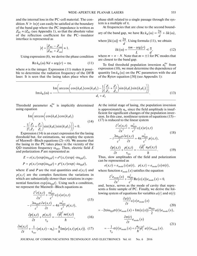
dition (27) shows that the lasing is started when theloss and gain averaged over the cavity mode are equal.Hence, the lasing threshold decreases when the field isconcentrated in the layers with amplification. For theabove PC parameters and the frequencies that arelower (higher) than the second band gap, the field inthe crystal is concentrated in the gain (loss) layers, sothat the threshold population inversions below andabove the band gap are significantly different (Fig. 2).Such a dependence is a manifestation of the Bor�rmann effect in the PC [31, 32].
To find the field amplitude above the lasing thresh�old, we must take into account nonlinear effects in the
0nthr0n
Re+
λ
ε
=
πτ
��
thr mode modemode mode
p
0 2
Im.
4
e ee n e
d
εmode modeIme e
mode mode0e n e
8
6
4
2
160140120110 130 150ωτ0
10–4n0
BG
Fig. 2. Plot of threshold population inversion of lasing vs.frequency (BG is the band gap corresponding to a linearPC and = + ).0τ 1(dπ 2)d c
JOURNAL OF COMMUNICATIONS TECHNOLOGY AND ELECTRONICS Vol. 61 No. 6 2016
WIDE�APERTURE PLANAR LASERS 557
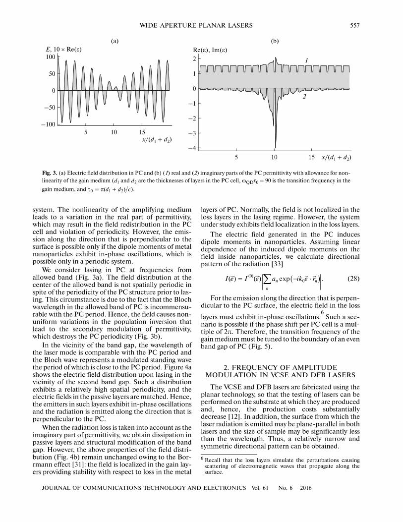
system. The nonlinearity of the amplifying mediumleads to a variation in the real part of permittivity,which may result in the field redistribution in the PCcell and violation of periodicity. However, the emis�sion along the direction that is perpendicular to thesurface is possible only if the dipole moments of metalnanoparticles exhibit in�phase oscillations, which ispossible only in a periodic system.
We consider lasing in PC at frequencies fromallowed band (Fig. 3a). The field distribution at thecenter of the allowed band is not spatially periodic inspite of the periodicity of the PC structure prior to las�ing. This circumstance is due to the fact that the Blochwavelength in the allowed band of PC is incommensu�rable with the PC period. Hence, the field causes non�uniform variations in the population inversion thatlead to the secondary modulation of permittivity,which destroys the PC periodicity (Fig. 3b).
In the vicinity of the band gap, the wavelength ofthe laser mode is comparable with the PC period andthe Bloch wave represents a modulated standing wavethe period of which is close to the PC period. Figure 4ashows the electric field distribution upon lasing in thevicinity of the second band gap. Such a distributionexhibits a relatively high spatial periodicity, and theelectric fields in the passive layers are matched. Hence,the emitters in such layers exhibit in�phase oscillationsand the radiation is emitted along the direction that isperpendicular to the PC.
When the radiation loss is taken into account as theimaginary part of permittivity, we obtain dissipation inpassive layers and structural modification of the bandgap. However, the above properties of the field distri�bution (Fig. 4b) remain unchanged owing to the Bor�rmann effect [31]: the field is localized in the gain lay�ers providing stability with respect to loss in the metal
layers of PC. Normally, the field is not localized in theloss layers in the lasing regime. However, the systemunder study exhibits field localization in the loss layers.
The electric field generated in the PC inducesdipole moments in nanoparticles. Assuming lineardependence of the induced dipole moments on thefield inside nanoparticles, we calculate directionalpattern of the radiation [33]
(28)
For the emission along the direction that is perpen�dicular to the PC surface, the electric field in the loss
layers must exhibit in�phase oscillations.6 Such a sce�
nario is possible if the phase shift per PC cell is a mul�tiple of 2π. Therefore, the transition frequency of thegain medium must be tuned to the boundary of an evenband gap of PC (Fig. 5).
2. FREQUENCY OF AMPLITUDE MODULATION IN VCSE AND DFB LASERS
The VCSE and DFB lasers are fabricated using theplanar technology, so that the testing of lasers can beperformed on the substrate at which they are producedand, hence, the production costs substantiallydecrease [12]. In addition, the surface from which thelaser radiation is emitted may be plane�parallel in bothlasers and the size of sample may be significantly lessthan the wavelength. Thus, a relatively narrow andsymmetric directional pattern can be obtained.
6 Recall that the loss layers simulate the perturbations causingscattering of electromagnetic waves that propagate along thesurface.
( )(0)0( ) ( ) exp .n n
n
I e I e a ik e r= − ⋅∑� � � �
100
50
0
–50
–10010 155
x/(d1 + d2)
E, 10 × Re(ε)(a)
2
1
–2
–3
–4
10 155 x/(d1 + d2)
Re(ε), Im(ε)
(b)
0
–1
1
2
Fig. 3. (a) Electric field distribution in PC and (b) (1) real and (2) imaginary parts of the PC permittivity with allowance for non�linearity of the gain medium ( and are the thicknesses of layers in the PC cell, ωQDτ0 = 90 is the transition frequency in the
gain medium, and = + ).1d 2d
0τ 1(dπ 2)d c

558
JOURNAL OF COMMUNICATIONS TECHNOLOGY AND ELECTRONICS Vol. 61 No. 6 2016
SHISHKOV et al.
The DFB and VCSE lasers are used in optoelec�tronics for the transformation of electric signal. Animportant characteristic for such applications is thefrequency of amplitude modulation in the presence ofrelatively small variations in the pump intensity that donot provide transition to the below�threshold regime[24, 34]. The frequency of the amplitude modulationis given by [24, 35] (see Appendix 2)
(29)
where is the photon number density inthe laser mode in the stationary state, s is the number
βω = +
τ τ τ
stmode
amen en sp
2 0 ,g S F
=
stmodeS s V
of photons in a mode, is the mode volume, isthe gain, = is the field�energy decay time inthe cavity, is the spontaneous decay time of the gainmedium in free space, is the Purcell factor of thecavity mode, and β is the ratio of the rate of spontane�ous decay to the cavity mode to the total rate of spon�taneous decay. The mode volume is calculated as
(30)
where the integration is performed over the entire
space and denotes the maximum value
of the expression in parentheses in the entire space.
For both VCSE and DFB lasers, we have owing to a relatively large number of modes to whichQDs may emit. Therefore, we may approximate themodulation frequency as
(31)
It is seen that the frequency of the amplitude mod�ulation in the VCSE and DFB lasers is limited.Indeed, an increase in results from an increase innumber s of photons in the cavity mode that can bereached using an increase in either Q factor or popula�tion inversion. An increase in the Q factor leads to adecrease in the modulation frequency, so that such amethod for an increase in the number of photons isinapplicable. An increase in population inversion nleads to an increase in the modulation frequency.However, the maximum possible population inversionis equal to the number density of atoms in the amplify�ing medium. In addition, the pump current that isneeded for the generation of population inversion
modeV 0gτen Q ω
τsp
modeF
( ) ( )
( ) ( )( )ε
=
ε
∫mode
max
2
2,
E dVV
E
r r
r r
( )εmax
2( ) ( )Er r
1β �
ωω =am
mode0 .sgV Q
ωmode
40
20
0
–20
–40155 2010
x/(d1 + d2)
E, Re ε(а)
10
5
0
–5
–10
155 2010x/(d1 + d2)
E, Re ε
(b)
Fig. 4. Electric field distribution in PC for = (a) 0.0 and (b) 0.5 and transition frequency in gain medium ωQDτ0 = 137 ( =
+ ).2Im ε 0τ
1(dπ 2)d c
0.10–0.05–0.10 0.05
1.0
0.8
0.6
0.4
0.2
α, rad
1
2
Iem(ωQDτ0 = 137), 1013 × Iem(ωQDτ0 = 90)
Fig. 5. Directional pattern of radiation for a periodic grat�ing of NPs at ωQDτ0 = (1) 90 and (2) 137. The angle plot�ted on the abscissa axis is measured relative to the directionperpendicular to the PC plane, the number of PC cells is
N = 40, the population inversion is and thethicknesses of the layers in the PC cell are d1 and d2.
30 10 ,n −
=

JOURNAL OF COMMUNICATIONS TECHNOLOGY AND ELECTRONICS Vol. 61 No. 6 2016
WIDE�APERTURE PLANAR LASERS 559
n = n0 exponentially increases with increasing n0 [12].Thus, the modulation frequency can hardly beincreased using an increase in the population inver�sion. Note that a relatively high photon density in thecavity may cause overheating and the damage of gainmedium.
An alternative approach to an increase in frequencyωam employs a decrease in laser mode volume Vmode. Inthis case, the modulation frequency increases due toan increase in both photon density in the mode andspontaneous decay rate. Indeed, the rate of spontane�ous decay of atom to the cavity mode differs from thedecay rate in free space by Purcell factor [24]
(32)
which is inversely proportional to the mode volume.In conventional VCSE and DFB lasers, the mode
volume is Vmode ≥ where S is the emitting sur�face and n is the refractive index for the cavity mode.Thus, the maximum frequency of the amplitude mod�ulation is fundamentally limited in the VCSE andDFB lasers [12]. Wide�aperture sources of coherentradiation based on spasers are being developed atpresent to eliminate the above limitation.
3. SPASERS AND PLASMON DFB LASERS
3.1. Spasers
There has been considerable recent interest in thesources of coherent radiation based on compositematerials containing plasmon nanostructures as alter�natives to lasers with cavities based on PCs [5–11].The key element of such structures is the generator ofcoherent plasmons (spaser) that was theoretically pre�dicted in 2003 [10, 36] and experimentally imple�mented in 2009 [37, 38]. A spaser schematically repre�sents a quantum–plasmon device consisting ofinversely excited QDs, atoms, or molecules that inter�act with plasmon nanoparticles [10, 36], plasmonwaveguides [37, 38], or surfaces. The working princi�ple of spaser is similar to the working principle of laserbased on the amplification provided by populationinversion and the feedback provided by the stimulatedemission of quantum system. The conditions for thestimulated emission of the inverse quantum system inthe presence of the wave field that is generated in thesame system are provided in the cavity that localizesthe generated mode. Surface plasmons of nanoparti�cles the localization of which on a nanoparticle pro�vides the conditions for positive feedback serve as theemitted field in the spaser. In other words, the genera�tion of near�fields of nanoparticles takes place in aspaser. The amplification of surface plasmons resultsfrom the nonradiative energy transfer [39] from QDs.The process is based on the near�field interaction of aQD and a plasmon nanoparticle. Such a process canbe considered as the basic process, since the probabil�
( )=
π λmode
mode2 3
3 ,4
QFV n
( )2 ,S nλ
ity of the nonradiative excitation of plasmon is greaterthan the probability of radiative emission of photon byfactor (krNP–QD)–3, where rNP–QD � λ is the distancebetween the centers of nanoparticle and QD and
Ohmic loss IJ and the loss related to the far�field emission of electromagnetic fields Iem are themain losses in the spaser. The ohmic loss in nanoparti�cle increases proportionally to the nanoparticle volume
(IJ ~ VNP ~ ), and the emission loss is proportional to
the squared volume of nanoparticle (Iem ~ ~ rNP is the radius of nanoparticle). Thus, the emission(ohmic) loss dominates at relatively large (small) sizesof nanoparticles when rNP ≥ 50 nm (rNP ≤ 20 nm).
The Purcell factor Fmode � 1 must be taken intoaccount in spaser owing to a relatively small volume ofthe laser mode Vmode ≈ VNP �λ3. If the frequency of thegain medium is tuned to the resonance with a mode ofnanoparticle (e.g., dipole mode), the rate of spontane�ous decay to such a mode is significantly higher thanthe total rate of the decay to the remaining modes
(see Appendix 2). Therefore, frequency of theamplitude modulation ωam in spaser may be signifi�cantly higher than the frequency in conventionallasers [40].
The main disadvantage of spasers that impedestheir application as sources of far�field electromag�netic radiation is related to (i) low efficiency of theconversion of pump current energy into the radiationenergy due to relatively high ohmic loss in nanoparti�cle and (ii) relatively wide directional pattern. The lat�ter is due to the fact that the size of spaser is substan�tially less than the wavelength of emitted radiation, sothat the directional pattern of a single spaser coincideswith the directional pattern of a single dipole.
The sources of coherent radiation with a relativelynarrow directional pattern can be based on the plas�mon DFB lasers [19, 40] that employ the matching ofplanar distributed emitters (2D arrays of spasers[16, 17, 28, 30]) and the systems based on light stopping.
3.2. Plasmon DFB Lasers
Plasmon DFB lasers slightly differ from conventionalDFB lasers. Therefore, they exhibit the main advantagesand disadvantages of the conventional systems.
The lasing in plasmon DFB lasers takes place atwaveguide modes that propagate along the surface ofthe system, and the radiation is emitted along thedirection that is perpendicular to the generation plane.The positive feedback in the system results from mul�tiple scattering by a periodic grating of perturbations
(metal nanoparticles or holes in metal film).7
The plasmon DFB lasers are divided into twoclasses. The lasers of the first class are based on dielec�
7 The grating of perturbations serves as the PC.
2 .k = π λ
NP3r
NP2V NP
6 ,r
( 1)β ≈
560
JOURNAL OF COMMUNICATIONS TECHNOLOGY AND ELECTRONICS Vol. 61 No. 6 2016
SHISHKOV et al.
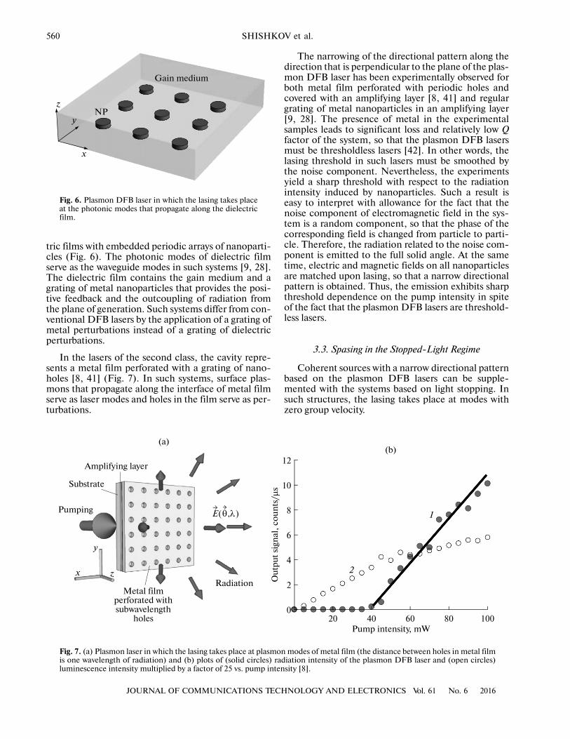
tric films with embedded periodic arrays of nanoparti�cles (Fig. 6). The photonic modes of dielectric filmserve as the waveguide modes in such systems [9, 28].The dielectric film contains the gain medium and agrating of metal nanoparticles that provides the posi�tive feedback and the outcoupling of radiation fromthe plane of generation. Such systems differ from con�ventional DFB lasers by the application of a grating ofmetal perturbations instead of a grating of dielectricperturbations.
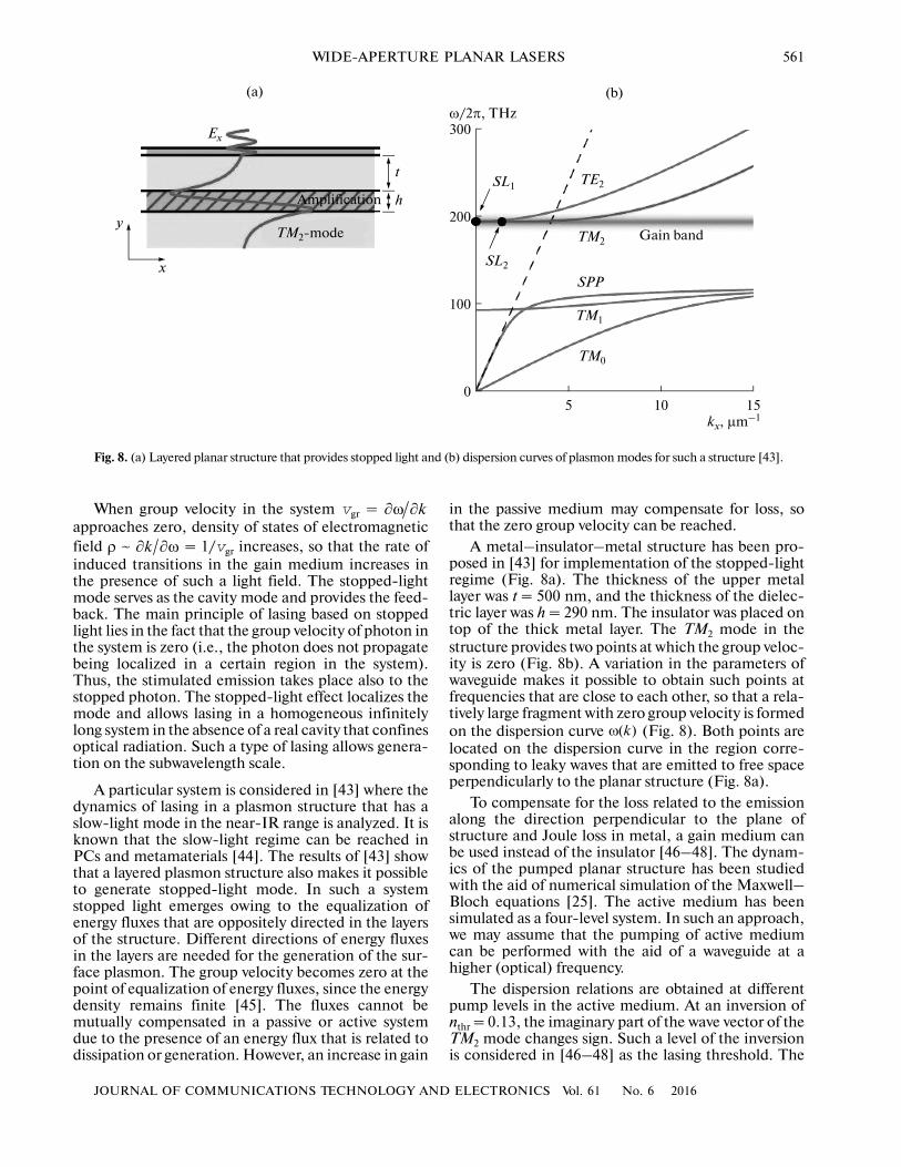
In the lasers of the second class, the cavity repre�sents a metal film perforated with a grating of nano�holes [8, 41] (Fig. 7). In such systems, surface plas�mons that propagate along the interface of metal filmserve as laser modes and holes in the film serve as per�turbations.
The narrowing of the directional pattern along thedirection that is perpendicular to the plane of the plas�mon DFB laser has been experimentally observed forboth metal film perforated with periodic holes andcovered with an amplifying layer [8, 41] and regulargrating of metal nanoparticles in an amplifying layer[9, 28]. The presence of metal in the experimentalsamples leads to significant loss and relatively low Qfactor of the system, so that the plasmon DFB lasersmust be thresholdless lasers [42]. In other words, thelasing threshold in such lasers must be smoothed bythe noise component. Nevertheless, the experimentsyield a sharp threshold with respect to the radiationintensity induced by nanoparticles. Such a result iseasy to interpret with allowance for the fact that thenoise component of electromagnetic field in the sys�tem is a random component, so that the phase of thecorresponding field is changed from particle to parti�cle. Therefore, the radiation related to the noise com�ponent is emitted to the full solid angle. At the sametime, electric and magnetic fields on all nanoparticlesare matched upon lasing, so that a narrow directionalpattern is obtained. Thus, the emission exhibits sharpthreshold dependence on the pump intensity in spiteof the fact that the plasmon DFB lasers are threshold�less lasers.
3.3. Spasing in the Stopped�Light Regime
Coherent sources with a narrow directional patternbased on the plasmon DFB lasers can be supple�mented with the systems based on light stopping. Insuch structures, the lasing takes place at modes withzero group velocity.
12
10
8
6
4
2
010040 6020 80
Pump intensity, mW
(b)
1
2
Out
put
sign
al,
coun
ts/µ
s
(а)
Amplifying layer
Substrate
Pumping
RadiationMetal film
perforated withsubwavelength
holes
zx
y
E θ λ,( )
Fig. 7. (a) Plasmon laser in which the lasing takes place at plasmon modes of metal film (the distance between holes in metal filmis one wavelength of radiation) and (b) plots of (solid circles) radiation intensity of the plasmon DFB laser and (open circles)luminescence intensity multiplied by a factor of 25 vs. pump intensity [8].
Gain medium
x
z
yNP
Fig. 6. Plasmon DFB laser in which the lasing takes placeat the photonic modes that propagate along the dielectricfilm.
JOURNAL OF COMMUNICATIONS TECHNOLOGY AND ELECTRONICS Vol. 61 No. 6 2016
WIDE�APERTURE PLANAR LASERS 561
When group velocity in the system vgr = approaches zero, density of states of electromagneticfield ~ = 1/vgr increases, so that the rate ofinduced transitions in the gain medium increases inthe presence of such a light field. The stopped�lightmode serves as the cavity mode and provides the feed�back. The main principle of lasing based on stoppedlight lies in the fact that the group velocity of photon inthe system is zero (i.e., the photon does not propagatebeing localized in a certain region in the system).Thus, the stimulated emission takes place also to thestopped photon. The stopped�light effect localizes themode and allows lasing in a homogeneous infinitelylong system in the absence of a real cavity that confinesoptical radiation. Such a type of lasing allows genera�tion on the subwavelength scale.
A particular system is considered in [43] where thedynamics of lasing in a plasmon structure that has aslow�light mode in the near�IR range is analyzed. It isknown that the slow�light regime can be reached inPCs and metamaterials [44]. The results of [43] showthat a layered plasmon structure also makes it possibleto generate stopped�light mode. In such a systemstopped light emerges owing to the equalization ofenergy fluxes that are oppositely directed in the layersof the structure. Different directions of energy fluxesin the layers are needed for the generation of the sur�face plasmon. The group velocity becomes zero at thepoint of equalization of energy fluxes, since the energydensity remains finite [45]. The fluxes cannot bemutually compensated in a passive or active systemdue to the presence of an energy flux that is related todissipation or generation. However, an increase in gain
k∂ω ∂
ρ k∂ ∂ω
in the passive medium may compensate for loss, sothat the zero group velocity can be reached.
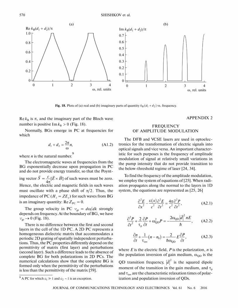
A metal–insulator–metal structure has been pro�posed in [43] for implementation of the stopped�lightregime (Fig. 8a). The thickness of the upper metallayer was t = 500 nm, and the thickness of the dielec�tric layer was h = 290 nm. The insulator was placed ontop of the thick metal layer. The TM2 mode in thestructure provides two points at which the group veloc�ity is zero (Fig. 8b). A variation in the parameters ofwaveguide makes it possible to obtain such points atfrequencies that are close to each other, so that a rela�tively large fragment with zero group velocity is formedon the dispersion curve (Fig. 8). Both points arelocated on the dispersion curve in the region corre�sponding to leaky waves that are emitted to free spaceperpendicularly to the planar structure (Fig. 8a).
To compensate for the loss related to the emissionalong the direction perpendicular to the plane ofstructure and Joule loss in metal, a gain medium canbe used instead of the insulator [46–48]. The dynam�ics of the pumped planar structure has been studiedwith the aid of numerical simulation of the Maxwell–Bloch equations [25]. The active medium has beensimulated as a four�level system. In such an approach,we may assume that the pumping of active mediumcan be performed with the aid of a waveguide at ahigher (optical) frequency.
The dispersion relations are obtained at differentpump levels in the active medium. At an inversion ofnthr = 0.13, the imaginary part of the wave vector of theTM2 mode changes sign. Such a level of the inversionis considered in [46–48] as the lasing threshold. The
( )kω
300
200
100
010 155
kx, μm–1
(b)
TE2
Gain band
SPP
TM2
TM1
TM0
SL1
SL2
ω/2π, THz
(a)
x
y
Amplification
Ex
TM2�mode
t
h
Fig. 8. (a) Layered planar structure that provides stopped light and (b) dispersion curves of plasmon modes for such a structure [43].

562
JOURNAL OF COMMUNICATIONS TECHNOLOGY AND ELECTRONICS Vol. 61 No. 6 2016
SHISHKOV et al.
narrowing of the laser line has been demonstrated. Inthe steady�state regime, the inversion in the activemedium n ~ 0.5 (Fig. 9a) is significantly greater thatthreshold level nthr calculated above. Such an increaseis due to the additional compensation for loss uponlasing (i.e., partial propagation of energy along thewaveguide that results from both group�velocity dis�persion and the formation of spatial wells caused bynonuniform distribution of electric field (Fig. 9b)).
Note that, in this case, the real part of the wave vec�tor is close to zero, so that the atomic oscillations inthe gain medium are matched in the spot the size ofwhich is inversely proportional to the real part of thewave number. In fact, the size of the lasing spot isdetermined by the pumping area and has subwave�length size, which impedes the formation of a narrowdirectional pattern.
Note also a possibility of spasing in the stopped�light regime for the plasmon mode that is located onthe dispersion curve outside the light cone and doesnot emit to free space. For example, the point withzero group velocity is observed for the TM1 mode inthe waveguide with a similar (metal–insulator–metal)structure and specific parameters of layers. In thiscase, the waves with k ≈ k2 (k2 is the wave number ofthe TM1 mode with zero group velocity) are involvedin the formation of the laser mode. Therefore, theelectromagnetic field of such a mode is modulated at afrequency of about In this case, the emission isabsent and the near�field is generated. Thus, such aregime can be called spasing in the absence of cavity.
3.4. Phase�Matching of a 2D Array of Spasers
2D spaser arrays can also be used for the develop�ment of coherent sources with relatively narrow direc�tional patterns. In accordance with the recent theoret�ical predictions of [5, 6, 49–51], the interaction of
2 .k∼π
spasers in a planar array may lead to phase matching ofthe field oscillations on single spasers and the narrow�ing of the directional pattern along the direction per�pendicular to the plane of array.
In fact, such systems represent PCs a unit cell ofwhich contains a scatterer surrounded by activemedium. The plasmon resonance emerges in the scat�terer at a certain frequency, a single cell is transformedinto a spaser, and the system becomes similar to thesystem of [49–51]. The difference lies in the fact thatthe analysis cannot be restricted to the dipole–dipoleinteraction of the spasers.
Two substantially different methods can be used formode locking in the 2D spaser array.
A rectangular grating of plasmon nanoparticleswith complicated shapes (Fig. 10) that are placed onthe surface of the active medium has been consideredin [5, 6]. For certainty, we assume that the gratingbelongs to the xy plane and the edges of grating areparallel to the x and y axes.
Owing to the periodicity of the grating, the field insuch a system can be represented as a series in terms ofstanding waves with wave numbers
where dx and dy are the distances between the neigh�boring nanoparticles along the x and y axes, respec�tively; Lx and Ly are the sizes of the system along theaxes; and nx and ny are the integers that range from 0 to
and from 0 to , respectively.The shape of nanoparticles in [5, 6] corresponds to
the minimum radiation intensity of the grating ofnanoparticles when the field distribution in the systemcoincides with the standing wave with = (phase matching). For such a shape of nanoparticles,the threshold pumping for the phase�matched mode is
{ }, , ,yxx y x y
x y
ddk k n n
L L
⎧ ⎫ππ= ⎨ ⎬⎩ ⎭
x xL d y yL d
{ },x yk k { }0,0
1.0
0.8
0.6
0.4
0.2
6040200 3010 50t, ps
Am
plit
ude,
arb
. un
its
2
1
(а) (b)
Rate of stimulatedemission
400 nm5.0
2.5
0
x
y
1012 s –
1
Fig. 9. (a) Plots of (1) field energy and (2) population inversion vs. time and (b) field distribution inside the waveguide uponlasing [43].

JOURNAL OF COMMUNICATIONS TECHNOLOGY AND ELECTRONICS Vol. 61 No. 6 2016
WIDE�APERTURE PLANAR LASERS 563
lower than the pumping for any mode of the system. Inany system of several spasers, which represents a mul�timode laser, the mode competition results in the sur�vival of the mode with the lowest pumping thresholdand the phase�matched distribution of currents isestablished in the system. Note two significant disad�vantages of such a method (the application of nano�particles with complicated shapes (Fig. 10a) and theminimization of the radiation intensity for the abovetype of phase matching) that impede the developmentof an efficient source of coherent radiation.
A method for the phase�matching of the oscilla�tions of dipole moments of single nanoparticles in a2D spaser array that is free of the above disadvantageshas been proposed in [49–51]. In such a method, atleast two nanoparticles interact with each QD in thespaser array [49–51]. Such interaction in the system ofspasers leads to the phase matching of the oscillationsof spasers that is maintained when the radiative loss istaken into account. The radiation power of an array ofphase�matched spasers per unit solid angle along thedirection perpendicular to the plane of array is propor�tional to the square of the number of spasers N2. Suchan increase is due to superradiance [52] at small sizesof the system (significantly less than the wavelength)and the narrowing of the directional pattern at largesizes. Thus, the system may serve as an efficient sourceof directional coherent radiation.
We consider a particular 2D periodic array of spas�ers. Two inverse QDs that are located in the vicinity ofa metal ellipsoid nanoparticle (NP) (Fig. 11a) serve asa model of spaser [49–51]. For simplicity, we assumethat the quantum system is a two�level system and theellipsoid nanoparticles that have dipole plasmonmodes serve as cavities. The eigenfrequencies of thedipole modes with different orientations are differentowing to the nonspherical shape of the nanoparticles.We assume that the frequency of the mode with the
dipole mode that is oriented along the major axis ofellipsoid coincides with the QD transition frequencyand the frequencies of the remaining dipole modessubstantially differ from the transition frequency and,hence, are not excited upon lasing in the system.
Let single spasers [49–51] form a 2D rectangulargrating. For definiteness, we assume that the gratingbelongs to the xy plane and the edges of the grating areparallel to the x and y axes (Fig. 11c). We also assumethat the distances between the nanoparticles along the xand y axes (δx and δy in Fig. 11b) are significantly lessthan the wavelength ( = = = in [49–51])and the system under study has a square shape with
side L and number of spasers N.8
The spaser dynamics is described using a system ofthree equations for amplitude of NP dipole moment a,polarization σ, and population inversion D of QD[53]. In the 2D array, the spaser with number =
interacts with the local field = that is generated by the spaser with
number = The projection of the local fieldof a single dipole along the direction of the dipolemoment of the nanoparticle is represented as
(33)
where is the wave number in vacuum, is theunit vector that is parallel to the NP dipole moment,
is the vector that connects spaser with number
8 A p–n junction can be used in practice as amplifying mediuminstead of QDs. In this case, the p–n junction is formed on aspecific substrate (e.g., InP) and, then, metal (gold or silver)NPs are deposited on the p–n junction.
Δ xδ yδ 20λ
n�
( ),x yn n n m ma−
Ω ⋅� � �
( )( )Ω − Δ ⋅ �
� �
mn m am�
( ), .x ym m
( )( )
( ) ( )( )
−
⎛ ⋅ −Ω = τ ⎜
⎝
⎞⋅ − ⋅ −− − ⎟
⎠
� �
�
� � � �
rad
21
3
2 22
0 02
3 1
3 1 1exp ,
x
x x
e eeR
R
e e e eik k ikR
RR
0k c= ω xe�
eR�
m�
Metalnanowire
Array of cavities
PumpingLaser
radiation
Gain medium
k
HE
β1
Laserradiation
β2
(а) (b)
Fig. 10. Schemes of (a) NP and (b) NP array [5].

564
JOURNAL OF COMMUNICATIONS TECHNOLOGY AND ELECTRONICS Vol. 61 No. 6 2016
SHISHKOV et al.
δxQD
x
yz
δyQD
δy δy
δx
δx
NP
QD
QD
NP
NPNP NP
NP
xz
y
(c)
(b)(а)
Fig. 11. (a) Scheme of a unit cell of a spaser array: ellipsoid NP that interacts with two QDs. (b) Mutual positions of neighboringNPs in the spaser array. (c) Phased array of spasers (the arrows show NPs (ellipsoids) and QDs (spheres) that interact with thecentral NP).

JOURNAL OF COMMUNICATIONS TECHNOLOGY AND ELECTRONICS Vol. 61 No. 6 2016
WIDE�APERTURE PLANAR LASERS 565
and spaser with number , and is the radiativedecay rate. For a spherical nanoparticle with radius rNP
in free space, we have = [53]. In
general, parameter depends on the environmentand shape of NP. At the frequency of the dipole reso�
nance ωres, parameter is related to polarizability:
For the calculation of the local field, we restrictconsideration to the dipole–dipole interaction (withallowance for the retardation effect (33)) of thenanoparticles and disregard the interaction withhigher multipoles. The expression for the local fieldis typical of free space, and a single effect that isrelated to the metal film and taken into account is thewave decay in free space (we have k = inexpression (33), and and in thenumerical simulation). When such a decay is nottaken into account, the NP interaction in a perfectsystem is not reduced to the interaction of neighbor�ing NPs, the finiteness of the sizes of structurebecomes significant, and we obtain nonuniformityover the array of local fields that are exerted on spas�ers and several instabilities. As for the remainingeffects, the qualitative influence of the local field onthe system under study is absent.
In the approximation of rotating wave [54–58], thesystem of interacting spasers is described using the sys�tem of nonlinear differential equations
(34)
(35)
n�
−
τrad1
−
τrad1 ( )
ω=ω
∂ε ∂ωres
NP3
02k r
−
τrad1
−
τrad1
( )α ω
−
−
ω=ω
τ = −∂α ∂ω
res
rad
31 0
12 .3
k
+' "k ik
' 0k k= " ' 0.2k k =
−
−
− = ≠
+ τ = − Ω σ + Ω∑ ∑� � � � � �
� � � �
� dnp r1
1
,n n m n m m
n m m n
a a i i a
−
− =
σ + τ σ = Ω ∑� � � �
� �
� dqd r1
1
,n n m m
n m
i a D
(36)
where is the dipole moment of the th nanoparti�cle, is the dipole moment and is the populationinversion of the th QD, and D0 is the external pumpintensity that is assumed to be equal for all QDs. Therelaxation times of polarization (transverse relaxation)and population inversion (longitudinal relaxation) ofQDs are τdqd and τiqd, respectively. The lifetime of theplasmon mode is determined by the Joule and radia�
tive losses: = + (in the calculations, we use
= ).In the system of equations (34)–(36), we take into
account the interaction of NPs (the second term onthe right�hand side in Eq. (34)) and the interaction ofNP with four neighboring QDs (the first term on theright�hand side in Eq. (34)). We also take into accountthe radiative loss that increases with an increase in thenumber of spasers. The system of equations (34)–(36)does not take into account the spontaneous emissionof QDs that is important in the vicinity of the generationthreshold. Hence the above system of equations can beused only substantially above the lasing threshold.
The numerical solution of the system of equa�tions (34)–(36) at that is significantly greater thana certain threshold level shows that the oscillations ofdipole moments of single spasers in the spaser arrayreach a stationary level with almost uniform phase dis�tribution over the array (Fig. 12). In the arrays with anumber of spasers N of about 102, we can reach almostperfect phase matching of the oscillations of dipolemoments in the system (Fig. 12a). In relatively large
systems , we obtain perturbations in thevicinity of boundaries along the direction that is paral�lel to the oscillations of dipole moments (Fig. 12b).Such an edge effect has a scale of about one wave�length in vacuum. When the sizes of the system are sig�
( )−
− =
+ τ − = Ω σ − σ∑� � � � � �
� �
�
iqd r1
0 1
1
* *2 ( ),n n m n m n
n m
D D D i a a
na � n�
nσ �
nD�
n�
−
τdnp1 −
τJ1 −
τrad1
−
τJ1 −
τ rad127
RΩ
2( 10 )N �
54
3
2
1 5
43
20
xy
arga
π
(a)
0
50
100 0
50
100
xy
arga
3π
(b)
π
Fig. 12. Distributions of the oscillation phases of dipole moments over the spaser array for (a) 5 × 5 and (b) 100 × 100 spaser arraysat (spaser numbers are plotted on the x and y axes, and the phase of the dipole moment is plotted on the z axis).Ω ≠r 0

566
JOURNAL OF COMMUNICATIONS TECHNOLOGY AND ELECTRONICS Vol. 61 No. 6 2016
SHISHKOV et al.
nificantly greater than the wavelength, the influence ofthe edge effects on the radiation intensity of a spaserarray and the directional pattern is negligible.
The phase�matched regime of oscillations of thedipole moments in the spaser array is reached owing tothe interaction of NPs and QDs of the neighboring NPs.
In the phase�matched regime, the far�field interac�tion of spasers leads to an increase in the radiation inten�sity. Such an effect is more developed for the systems withsmall sizes for which expression (33) is rep�resented as
(37)
where ≈ When the dipoles oscillate withidentical phases and amplitudes, the last term inexpression (34) can be divided into two parts:
(38)
The second term on the right�hand side in expres�sion (38) leads to an increase in the loss rate for the
th plasmon by a factor of . Hence, the effec�
tive decay rate is + and Eq. (34) can be rep�resented as
(39)
Thus, the dipole moments of NPs at pro�vide identical contributions to the radiation intensity
of each NP: = In this case, the total radi�
0( 1)k R �
( )( )
−
⎛ ⎞⋅ −Ω ≈ τ +⎜ ⎟
⎝ ⎠
� �
�
rad
21
3
3 13 ,2
xe eeR i
R
( )Im eR�
−
τrad1 .
( )
− − −
≠ ≠ ≠
−
−
≠
Ω = Ω − Ω
= Ω − − τ
∑ ∑ ∑
∑
� � � � � � � � �
� � � � � �
� � � �
� �
1
Re Im
Re 1 .
n m m m n m m n m
m n m n m n
m n m m R
m n
i a ia a
ia a N
�
n ( )1N −
−
τJ1 −
τrad1N
( )− −
−
− = ≠
+ τ + τ
= − Ω σ + Ω∑ ∑� �
� � � �
� � � �
� J rad
r
1 1
1
1
Re .
n n
m n m m
n m m n
a N a
i i a
0 1k R �
−
τrad_eff1 −
τrad1 .N
ation intensity of N NPs is proportional to the squareof the total number N2, which is typical of the superra�diance [52]. Note that such a dependence is obtainedwith the aid of the expression for the total field ofdipole with allowance for retardation (33). Therefore,all terms must be taken into account in expression (33)to correctly describe the effect of radiation on theoscillation dynamics of dipole moments in the spaserarray.
The radiation power of the spaser array can beobtained using the equations of energy balance thatfollow from expression (39) for the stationary regime:
(40)
In accordance with expression (37), we have ≈
for Thus, the term in sum
can be taken into account as = The left�hand side of Eq. (40) is proportional to the energy lossin the system. The first term on the right�hand sidecorresponds to the Joule loss, and the second termcorresponds to radiative loss I:
(41)
where q is the electron charge. Figure 13a presents thedependence of the power of radiative loss on the num�ber of spasers in the array.
At relatively small sizes of the system, the spasers
exhibit the in�phase oscillations ( for the aboveparameters) (Fig. 12a). In this case, the radiationintensity per one spaser linearly increases with anincrease in the number of spasers: = ~ For
( )
− =
−
−
⎡ ⎤Ω σ + Ω σ⎢ ⎥⎣ ⎦
= τ + Ω
∑ ∑
∑ ∑
� � � �
� � �
� � � � �
� � �
r r
J
1
1
21
,
* *Im( ) Im( )
*Im Re( ).
n n n m
n m n
n n m n m
n n m
a a
a a a
( )Im eR�
−
τrad1
0 1.k R � n m=
� �
,n m∑ � �
Im n m−Ω � �
−
τrad1 .
( )2
2
,
*Im Re( ),n m n m
n m
mI a aq
−
ω= Ω∑ � � � �
� �
210N <
1I I N .N
80
60
40
20
0800040000 60002000
40
30
20
10
40200 3010 50
N
I/N
8000
6000
4000
2000
0800040000 60002000 N
I/N(a) (b)
Fig. 13. Plots of (a) integral (with respect to angle) radiation intensity and (b) radiation intensity per one spaser along the directionthat is perpendicular to the plane of array vs. number of spasers: (dashed lines) perfectly matched system and (solid line) real sys�tem. The inset shows the dependence for a relatively small number of spasers.

JOURNAL OF COMMUNICATIONS TECHNOLOGY AND ELECTRONICS Vol. 61 No. 6 2016
WIDE�APERTURE PLANAR LASERS 567
such arrays, the radiation intensity coincides with theradiation intensity of a perfectly phase�matched sys�tem (see inset to Fig. 13a). With a further increase inthe size of the array, the radiation intensity decreasesdue to the formation of boundary states (Fig. 12b). Afurther increase leads to the phase�matching of themajor part of the array (Fig. 12b). For the number of
spasers , the radiation intensity of the sys�tem under study becomes approximately equal to theradiation intensity of a perfectly matched system andthe total radiation intensity decreases. Such a decreaseresults from the destructive interference of the dipolemoments of spasers that are located in different partsof the system. The equality of the radiation intensitiesof the system under study and the perfectly matchedsystem is due to negligible influence of the edge effectsat relatively large sizes of the spaser array.
For practical applications, the total radiationintensity of the system of spasers is less important thanthe radiation intensity per unit solid angle along thedirection perpendicular to the plane of array (i.e., theradiation power that is measured using a small detectorthat is placed above the plane of spaser array). We cancalculate the total radiation power of the system ofdipoles taking into account the interaction in the sys�tem via the total radiation field. However, such anapproach is inapplicable in the calculation of theangular distribution of the radiation intensity. Such adistribution can be obtained with the aid of the elec�trodynamic analysis of radiation for the calculated dis�tribution of amplitudes and phases of NP dipolemoments in the phase�matched spaser array. In other,words, we consider a system of spasers as a phasedantenna array. The angular distribution of the radia�tion of such an antenna can be obtained using the Fou�rier transform of the current distribution over its aper�ture [33]. For the system under study, we must use thedistribution of phases and amplitudes of dipolemoments over the system of spasers. Thus, the angulardistribution of the radiation intensity is given by
(42)
where is the unit vector along the direction of emis�sion, is the coordinate vector of the th dipole in the
array, and = is the radiationintensity of a single dipole along vector The integra�tion of expression (42) over all directions e yieldsexpression (41). Along the direction that is perpendic�
ular to the plane, we have = and
obtain dependence for the phase�matchedsystem with any size.
Such a conclusion is proven by the results ofnumerical calculation (Fig. 13b). It is of interest that alinear increase in ratio is determined by twoeffects. At relatively small sizes of the system (L < λ),
35 10N > ×
( ) ( ) ( )20
0exp ,n n
n
I e I e a ik e r= − ⋅∑ � �
�
� � � �
e�
nr��
n�
( )0I e�
( )18 −
π24
0 [ ]xck e e×
� �
.e�
( )I e�
( )0I e� ∑ �
�
2
nna
I N N∼
I N
such an increase results from an increase in the inte�gral radiation intensity due to the superradiance [52].At , an increase in ratio is caused by thenarrowing of the directional pattern due to an increasein the aperture of the emitting system (Fig. 14).
The numerical study of the 2D spaser array showsthat the interactions of NPs with QDs of the neighbor�ing NPs leads to the phase�matching of the oscilla�tions of dipole moments of single spasers. A modewith the lowest threshold with respect to pumpingDthr normally survives in multimode lasers in thepresence of mode competition [49, 50, 54–59]. Forthe system of spasers, the threshold with respect topumping is given by
Such a threshold is identical to the threshold of asingle spaser [53] with effective parameters Ωr, τdnp,and mismatch δ
(43)
(44)
(45)
where is the wave number of the eigen�mode of dipole oscillations in the spaser array.
Quantity depends on three factors
, and The first term
exhibits minimum at Indeed, in the phase�matched mode, the fields of the neighboring NPsinterfere on QDs, so that the corresponding interac�tions and energy transfer reach maximum levels for thephase�matched mode. Such an effect has been ana�lyzed in [50]. On the other hand, the second term
increases with increasing owing to anincrease in the radiative loss, so that quantity Dthr
increases. With regard to this factor, the mismatchedmode must have the lowest threshold. At the same
time, the third term tends to unity
when parameter increases.Thus, the stationary mode in the system results
from the competition of two effects: phase�matchingrelated to the nonlinear dipole–dipole interaction ofNPs with neighboring QDs and mismatching relatedto an increase in the radiation intensity.
The first effects dominates at realistic parameters.
Hence, the mode with has the lowest thresholdand will be observed in the stationary regime.
The above theory can be used only for an infinite2D array of spasers, since, in accordance with theassumption, the threshold and frequency of lasing areidentical for all of spasers in the array. A system with
L > λ I N
( ) ( )− − −
= Ω τ τ + δ τ
�
thr r eff dnp eff dqd eff dnp eff2 1 1 2 2_ _ _1 .D k
( )Ω = Ω Δ + Δr eff r_ 2 cos cos ,x yk k
( )− − −
τ = τ + Δ Ω∫�
�
dnp eff J1 1 2 2
_ ,eR d R
( ) ( )−
−
δ ≈ τ Δ Δ − Δeff rad31
03 2 cos cos ,x yk k k
( ),x yk k k=
�
�
thr( )D k −
Ωr eff2_ ,
−
τdnp eff1
_ ( )+ δ τeff dnp eff2 2
_1 . −
Ωr_eff2
0.k =
�
−
τdnp eff1
_ k�
( )+ δ τeff dnp eff2 2
_1−
τdnp eff1
_
0k =
�

568
JOURNAL OF COMMUNICATIONS TECHNOLOGY AND ELECTRONICS Vol. 61 No. 6 2016
SHISHKOV et al.
finite sizes exhibits edge effects at the boundaries(Fig. 12b) that lead to a decrease in the radiationintensity when the size of structure is on the order ofwavelength (Fig. 13a).
The edge effects are due to the shift of the fre�quency of the plasmon resonance of NPs at theboundaries relative to the resonance frequency of NPsat the center of the array. Indeed, the frequency of theNP plasmon resonance depends on the environment.At the center of the system, the environments areidentical and, hence, the shifts of the resonance fre�quency are also identical. For the spasers at the bound�aries, the environment differs from that at the center ofthe system, so that the frequency of the NP plasmonresonance at the boundary differs from the resonancefrequency of the same NP that is located at the center.
To compensate for the edge effects in the array, wemust change the mutual positions of NPs at the edgesof the system in such a way that the frequencies of plas�mon resonances become identical. Figure 15 showsthe positions of NPs at the boundary of the array atwhich the resonance frequencies are identical forall NPs.
In the resulting system, the presence of boundarydoes not affect the phase distribution of dipole
(а)
z
x
y z
x
y
(b)
Fig. 14. Directional pattern for the phase�matched spaser array for the system of (a) 5 × 5 and (b) 100 × 100 spasers.
α–α –α
–α–α
–β1
α
α
2α
–β2
Fig. 15. Position of NPs in the vicinity of the boundary ofthe phase�matched spaser array at which the field on NPsdoes not depend on the NP position in the array at α =
β1 = and β2 =
where = and are the distances between theneighboring NPs along the directions that are perpendicu�lar and parallel to the boundary of array, respectively.
3 ,d yδ�
( )31.263 ,6d yδ�
( )30.736 ,4d yδ�
xδ 23δy yδ

JOURNAL OF COMMUNICATIONS TECHNOLOGY AND ELECTRONICS Vol. 61 No. 6 2016
WIDE�APERTURE PLANAR LASERS 569
moments. The results of numerical simulation provesuch a conclusion (Fig. 16).
Thus, the radiation intensity of the system understudy and a perfectly matched system coincide at anynumber of spasers in the array (Fig. 17).
CONCLUSIONS
Modern plasmon wide�aperture lasers [9, 28, 41]predominantly represent plasmon DFB lasers. Suchlasers exhibit the generation of the Bloch wave at theedge of the second band gap. Plasmon DFB lasers arefree of strict limitations on the frequency of the ampli�tude modulation that are typical of DFB and VCSElasers. Thus, the former, can be used in optoelectron�ics for transformation of electric signal into opticalsignals and vice versa.
Devices based on cooperative phase�matching ofemitters with the generation of a wave with zero tan�gential wave vector may serve as alternatives to theplasmon DFB lasers. Note, for example, lasers withcavities on the stopped�light mode and 2D spaserarrays.
The main principle of lasing with the aid of stoppedlight is based on the fact that the group velocity of pho�tons in such devices is zero, so that photons do notpropagate and appear to be localized in certain regioninside the system. The resulting stimulated emissiontakes place to the same stopped photons, so that thelasing can be obtained in homogeneous infinitely longmedium in the absence of a real cavity that confinesthe radiation. Such an effect allows lasing on the sub�wavelength scale.
In a 2D spaser array, the interaction of NPs via QDsof the neighboring spasers may lead to the phase�matching of the oscillations of dipole moments of sin�gle NPs. When the aperture of the array is sufficient,
the directional pattern becomes relatively narrow andthe total radiation intensity increases by two orders ofmagnitude due to superradiance. Such devices areinteresting for applications in systems of open opticalcommunications. In particular, the first optical phasedarray can be developed.
APPENDIX 1
BAND STRUCTURE OF PC
PCs represent structures in which the permittivityexhibits periodic variation along one, two, or threeaxes in space. PCs are classified as 1D, 2D, and 3Dwith respect to the number of directions along whichthe permittivity is varied.
The properties of a linear 1D PC are well studied,the electric�field distribution in such a structure satisfiesthe Floquet–Bloch theorem: =
where = and kB is the Bloch wave num�ber. When the PC consists of two alternating layerswith thicknesses and , permittivities ε1 and ε2, andpermeabilities μ1 and μ2, respectively, the Bloch wavenumber can be calculated using the Rytov formula [30]
(A1.1)
where k1 = and k2 = are the wavevectors in the first and second media, respectively, andZ1 and Z2 are the corresponding impedances. Thepresence of band gaps (BGs) in the spectrum is animportant property of PCs. Electromagnetic waveswith frequencies from BG exponentially decay in thedepth of PC, the real part of the Bloch wave number
( )yE x ( ) ( )Bexp ,ik x f x
( )f x ( )f x L+
1d 2d
( )( ) ( ) ( )
( ) ( )
+ =
⎛ ⎞− +⎜ ⎟
⎝ ⎠
B 1 2 1 1 2 2
1 21 1 2 2
2 1
cos cos cos
1 sin sin ,2
k d d k d k d
Z Zk d k d
Z Z
ω ε μ1 1 c 2 2 cω ε μ
1020
30400
1
2
3
1020
3040
y
x
aargπ
���������
Fig. 16. Distribution of the oscillation phases of dipolemoments over the spaser plane for the 40 × 40 spaser arrayin which the edge effects along the x axis are compensatedfor (see Fig. 15).
25
20
15
10
5
4002000 300100N
I/N
Fig. 17. Plots of radiation intensity per one spaser in thephase�matched array vs. number of spasers for (dashedline) perfectly matched and (solid line) real systems.
570
JOURNAL OF COMMUNICATIONS TECHNOLOGY AND ELECTRONICS Vol. 61 No. 6 2016
SHISHKOV et al.
is π, and the imaginary part of the Bloch wavenumber is positive (Fig. 18).
Normally, BGs emerge in PC at frequencies forwhich
(A1.2)
where n is the natural number.9
The electromagnetic waves at frequencies from theBG exponentially decrease upon propagation in PCand do not provide energy transfer, so that the Poynt�
ing vector = of such waves must be zero.
Hence, the electric and magnetic fields in such wavesmust oscillate with a phase shift of Thus, theimpedance of PC ( = ) for such waves from BG
is an imaginary quantity: = 0.
The group velocity in PC vgr = stronglydepends on frequency. At the boundary of BG, we havevgr → 0 (Fig. 18).
There is no difference between the first and secondlayers in the cell of the 1D PC. A 2D PC represents ahomogeneous dielectric matrix that accommodates aperiodic 2D grating of spatially independent perturba�tions. Thus, the PC properties differently depend on thepermittivity of matrix (first layer) and perturbations(second layer). Such a difference leads to the absence ofcomplete BG for both polarizations in 2D PCs. Thenumerical calculations show that the complete BG isformed only when the permittivity of the perturbationsis less than the permittivity of the matrix [59].
9 A PC for which and is an exception.
BRe k>BIm 0k
1 22 ,d d nπ+ =
ω
1 1ε � ε ∼2 1
S�
[ ]4c E H×
π
� �
2.π
zH yZE
PCRe Z
d dkω
APPENDIX 2
FREQUENCY OF AMPLITUDE MODULATION
The DFB and VCSE lasers are used in optoelec�tronics for the transformation of electric signals intooptical signals and vice versa. An important character�istic for such purposes is the frequency of amplitudemodulation of signal at relatively small variations inthe pump intensity that do not provide transition tothe below�threshold regime of laser [24, 34].
To find the frequency of the amplitude modulation,we employ the system of equations of [25]. When radi�ation propagates along the normal to the layers in 1Dsystem, the equations are represented as [25, 26]
(A2.1)
(A2.2)
(A2.3)
where E is the electric field, P is the polarization, n isthe population inversion of gain medium, ωQD is the
QD transition frequency, is the squared dipolemoment of the transition in the gain medium, and τp
and τinv are the characteristic relaxation times of polar�ization and population inversion of QDs.
( )2 2 2
2 2 2 2 24 ,
xE E Px c t c t
ε∂ ∂ π∂− =
∂ ∂ ∂
ω∂ ∂+ + ω = −τ ∂∂
�
�
QDQD
p
22
2
2
22 ,d nEP P P
tt
( )∂ ∂+ − =
∂ τ ω ∂�inv QD0
1 2 ,n Pn n Et t
2d�
1.0
0.8
0.6
0.4
0.2
020 31 4
ω, rel. units
Re kB(d1 + d2)/π(а)
0.5
0.4
0.3
0.2
0.1
020 31 4
ω, rel. units
Im kB(d1 + d2)/π
0.6
0.7
(b)
Fig. 18. Plots of (a) real and (b) imaginary parts of quantity vs. frequency.( )+B 1 2k d d
JOURNAL OF COMMUNICATIONS TECHNOLOGY AND ELECTRONICS Vol. 61 No. 6 2016
WIDE�APERTURE PLANAR LASERS 571
The electric field and polarization can be written as
(A2.4)
(A2.5)
where is the mode of the system that satisfiesequation
and ωmode is the mode frequency. Variations in complexfunctions and are significantly slower than vari�ations in exponential function We assumethat which is valid for the VCSE anddielectric DFB lasers. Thus, expressions (A2.1)–(A2.3)can be represented as
(A2.6)
(A2.7)
(A2.8)
We substitute expression (A2.7) in expressions (A2.6)and (A2.8), multiply expression (A2.6) by , andaverage spatial factors in expressions (A2.6) and(A2.8) with respect to the mode of the system corre�sponding to frequency ωmode:
Thus, we derive equations to determine number den�
sity of photons in the cavity = and number density of carriers :
(A2.9)
(A2.10)
( ) ( ) ( )
( ) ( ) ( )
= ω
+ − ω
mode mode
mode mode*
exp
* exp ,
E a t e x i t
a t e x i t
( ) ( ) ( )
( ) ( ) ( )
= σ ω
+ σ − ω
mode mode
mode mode*
exp
* exp ,
P t e x i t
t e x i t
( )modee x
( )( ) ( )
∂ ω+ ε =
∂
mode modemode
2 2
2 20,
e xx e x
x c
( )a t ( )tσ
( )ωmodeexp .i tτ ωp mode ,Q�
( )( ) ( ) ( ) ( )
∂ε = − π ω σ
∂mode mode mode2 ,
a te x x i e x t
t
( ) ( ) ( )− ω
σ =
ω −ω + ω τ
��QD
QD mode mode p
2
2 2
2, ,
2
dt a t n x t
i
( )( )( )
( ) ( ) ( ) ( ) ( ) ( )( )
∂+ −
∂ τ
ω= − σ − σ
ω�
inv
modemode mode
QD
* *
0, 1 ,
2 * .
n x tn x t n
t
ie x e x a t t a t t
( )*a t
( ) ( ) ( )
( ) ( )=
∫∫mode mode
mode mode
*.
*
e x f x e x dxf
e x e x dx
( )S t ( )2a tε
− −
ω� mode1 1
( )N t
( )
( )πω ω τ∂
=∂ εω −ω + ω τ
��mode QD p
QD mode mode p
22
22 2 2 2
8,
4
dS SNt
( )
( )
( )
∂+ −
∂ τ
πω τ=
εω −ω + ω τ
��
inv
mode p
QD mode mode p
0
23
22 2 2 2
1
8.
4
N N Nt
d SN
If Eqs. (A2.9) and (A2.10) can berepresented as
(A2.11)
(A2.12)
where
We restrict consideration to the scenario in whichthe frequency of cavity coincides with the frequency ofthe gain band (ωmode = ωQD) and obtain
(A2.13)
(A2.14)
The Maxwell–Bloch equations do not take intoaccount spontaneous decays in the system. To takeinto account such processes, we supplement the equa�tions with the corresponding terms [19, 24]:
(A2.15)
(A2.16)
where is the gain, τen = is the decay time of thefield energy in the cavity, τsp is the spontaneous decaytime of the gain medium in free space, is thespontaneous decay rate to the laser mode, and Frem/τsp
is the spontaneous decay rate to the remaining modes.The amplitude modulation of the signal results
from the time�dependence of quantity N0. In the pres�ence of relatively weak amplitude modulation, thefield and population inversion weakly depend on timeand appear to be above the lasing threshold at any timemoment, so that quantities , and canbe represented as
(A2.17)
(A2.18)
(A2.19)
where , and are the stationary states of thesystem of equations (A2.15) and (A2.16). We substituteEqs. (A2.17)–(A2.19) to system of equations (A2.15)
ω − ω ωQD mode QD,�
( )πω∂
= ρ ω∂ ε
�
�
QD
28
,dS SN
t
( ) ( )πω∂
+ − = ρ ω∂ τ ε
�
�
mode
inv
2
0
81 ,dN SNN N
t
( )( )
τρ ω =
ω − ω + τ
p
QD mode p2 2
1.
1
πω τ∂=
∂ ε
�
�
QD p
22
,dS SN
t
( )πω τ∂
+ − =∂ τ ε
�
�
QD p
inv
2
0
21 .dN N N SN
t
= − +
τ τ
mode
en sp0 ,
FdS Sg SN Ndt
− += − −
τ τ
mode rem
inv sp
00 ,
N N F FdN g SN Ndt
0g Q ω
τmode spF
( ),S t ( )N t ( )0N t
( ) ( ) ( )[ ]= + ω ω
st Re exp ,S t S s i t
( ) ( ) ( )[ ]= + ω ω
st Re exp ,N t N n i t
( ) ( ) ( )[ ]= + ω ω
st0 0 0Re exp ,N t N n i t
st,S stN st0N

572
JOURNAL OF COMMUNICATIONS TECHNOLOGY AND ELECTRONICS Vol. 61 No. 6 2016
SHISHKOV et al.
and (A2.16) and use parameters Sst, Nst, and toobtain
(A2.20)
where
(A2.21)
is the frequency of amplitude modulation and β = is the ratio of the spontaneous
decay rate to the laser mode to the spontaneous decayrate to the remaining modes.
REFERENCES
1. X. Jiang and C. M. Soukoulis, Phys. Rev. B 59, 6159(1999).
2. S. Strauf, K. Hennessy, M. T. Rakher, et al., Phys. Rev.Lett. 96, 127404 (2006).
3. M. Imada, A. Chutinan, S. Noda, and M. Mochizuki,Phys. Rev. B 65, 195306 (2002).
4. M. Notomi, H. Suzuki, T. Tamamura, and K. Edagawa,Phys. Rev. Lett. 92, 123906 (2004).
5. N. I. Zheludev, S. L. Prosvirnin, N. Papasimakis, andV. A. Fedotov, Nature Photon 2, 351 (2008).
6. Y.�W. Huang, W. T. Chen, P. C. Wu, et al., Sci. Rep. 3,1237 (2013).
7. J. Y. Suh, C. H. Kim, W. Zhou, et al., Nano Lett. 12,5769 (2012).
8. F. Beijnum, P. J. Veldhoven, E. J. Geluk, et al., Phys.Rev. Lett. 110, 206802 (2013).
9. W. Zhou, M. Dridi, J. Y. Suh, et al., Nat. Nanotechnol.8, 506 (2013).
10. I. E. Protsenko, A. V. Uskov, O. A. Zaimidoroga, et al.,Phys. Rev. A 71, 063812 (2005).
11. I. E. Protsenko, A. V. Uskov, K. E. Krotova, andE. P. O’Reilly, J. Phys.: Conf. Ser. 107, 012010 (2008).
12. N. N. Ledentsov and D. A. Lott, Usp. Fiz. Nauk 181,884 (2011).
13. K. Iga, IEEE J. Sel. Top. Quantum Electron. 6, 1201(2000).
14. C. J. Chang�Hasnain, IEEE J. Sel. Top. QuantumElectron. 6, 978 (2000).
15. G. Steinle, H. Riechert, and A. Y. Egorov, Electron.Lett. 37, 93 (2001).
16. W. Yuen, G. S. Li, R. F. Nabiev, et al., Electron. Lett.36, 1121 (2000).
17. F. Koyama, J. Lightwave Technol. 24, 4502 (2006).
18. J. A. Lott, V. A. Shchukin, N. N. Ledentsov, et al., Elec�tron. Lett. 47, 717 (2011).
19. L. A. Coldren and S. W. Corzine, Diode Lasers andPhotonic Integrated Circuits (Wiley, New York, 1995).
st0N
( )
( )
ω ω τ τ=
ω ω − ω − γω
am en inv
am
2
2 20
,s
n i
βω = +
τ τ τ
stmode
amen en sp
2 0g S F
( )+mode mode remF F F
20. A. A. Zyablovskii, A. V. Dorofeenko, A. A. Pukhov,A. P. Vinogradov, E. S. Andrianov, A. B. Granovskii,and A. A. Lisyanskii, J. Commun. Technol. Electron.60, 87 (2015).
21. H. J. Unold, S. W. Z. Mahmoud, R. Jager, et al., IEEEPhotonics Technol. Lett. 12, 939 (2000).
22. C. Degen, W. Elsaber, and I. Fischer, Opt. Express 5(3), 38 (1999).
23. P. V. Mena, J. J. Morikuni, S. M. Kang, et al., J. Light�wave Technol. 17, 865 (1999).
24. D. Englund, H. Altug, B. Ellis, and J. Vuckovic, LaserPhot. Rev. 2, 264 (2008).
25. G. L. Lamb, Rev. Mod. Phys. 43 (2), 99 (1971).
26. A. V. Dorofeenko, A. A. Zyablovskii, A. A. Pukhov,et al., Usp. Fiz. Nauk 182, 1157 (2012).
27. A. A. Zyablovskii, A. V. Dorofeenko, A. A. Pukhov, andA. P. Vinogradov, J. Commun. Technol. Electron. 56,1139 (2011).
28. A. H. Schokker and A. F. Koenderink, Phys. Rev. B 90,155452 (2014).
29. A. A. Zyablovsky, A. V. Dorofeenko, A. P. Vinogradov,and A. A. Pukhov, Photonics Nanostruct. Fundam.Appl. 9, 398 (2011).
30. S. M. Rytov, Zh. Eksp. Teor. Fiz. 29, 605 (1955).
31. A. P. Vinogradov, Y. E. Lozovik, A. M. Merzlikin, et al.,Phys. Rev. B. 80, 235106 (2009).
32. S.�L. Chua, Y. Chong, A. D. Stone, et al., Opt. Express19, 1539 (2011).
33. C. A. Balanis, Antenna Theory – Analysis and Design,3rd Ed. (Wiley�Intersci., New York, 2005).
34. A. Mutig and D. Bimberg, Advances Opt. Technol.2011, 290508 (2011).
35. H. Altug, D. Englund, and J. Vuckovic, Nature Phys. 2,484 (2006).
36. D. J. Bergman and M. I. Stockman, Phys. Rev. Lett. 90,027402 (2003).
37. M. A. Noginov, G. Zhu, A. M. Belgrave, et al., Nature460, 1110 (2009).
38. Y.�J. Lu, J. Kim, H.�Y. Chen, et al., Science 337, 450(2012).
39. A. A. Kolokolov and G. V. Skrotskii, Usp. Fiz. Nauk162 (12), 165 (1992).
40. M. I. Stockman, J. Opt. 12, 024004 (2010).
41. X. Meng, J. Liu, A. V. Kildishev, and V. M. Shalaev,Laser Phot. Rev. 8, 896 (2014).
42. M. T. Hill, M. Marell, E. S. P. Leong, et al.,Opt. Express 17, 11107 (2009).
43. T. Pickering, J. M. Hamm, A. F. Page, et al., Nat.Commun. 5, 4972 (2014).
44. P. W. Milonni, Fast Light, Slow Light and Left�HandedLight (IOP Publishing, London, 2005).
45. V. M. Agranovich, Surface Polaritons: ElectromagneticWaves on Surfaces and Interfaces, Ed. by V.M. Agranov�ich and D.L. Mills (Nauka, Moscow, 1985) [in Rus�sian].
JOURNAL OF COMMUNICATIONS TECHNOLOGY AND ELECTRONICS Vol. 61 No. 6 2016
WIDE�APERTURE PLANAR LASERS 573
46. S. A. Ramakrishna, J. B. Pendry, M. C. K. Wiltshire,and W. J. Stewart, J. Mod. Opt. 50, 1419 (2003).
47. A. N. Lagar’kov, A. K. Sarychev, V. N. Kisel’, andG. Tartakovskii, Usp. Fiz. Nauk 179, 1018 (2009).
48. A. K. Sarychev, A. A. Pukhov, and G. Tartakovsky,PIERS Online 3, 1264 (2007).
49. A. V. Dorofeenko, A. A. Zyablovsky, A. P. Vinogradov,et al., Opt. Express 21, 14539 (2013).
50. E. S. Andrianov, A. A. Pukhov, A. V. Dorofeenko, et al.,Phys. Rev. B 85, 165419 (2012).
51. A. A. Zyablovsky, A. V. Dorofeenko, A. P. Vinogradov,et al., AIP Conf. Proc. 1475, 185 (2012).
52. R. H. Dicke, Phys. Rev. 93, 99 (1954).
53. E. S. Andrianov, A. A. Pukhov, A. V. Dorofeenko, et al.,Opt. Express 19, 24849 (2011).
54. A. N. Oraevskii, Kvant. Elektronika 29 (2), 37 (1999).
55. S. Solimeno, B. Crosignani, and P. Di Porto, Guiding,Diffraction and Confinement of Optical Radiation (Aca�demic, Orlando, 1986; Mir, Moscow, 1989).
56. Ya. I. Khanin, Principles of Laser Dynamics (Nauka,Moscow, 1999) [in Russian].
57. R. H. Pantell and H. E. Puthoff, Fundamentals ofQuantum Electronics (Wiley, New York, 1969; Mir,Moscow, 1972).
58. M. O. Skalli and M. S. Zubairi, Quantum Optics (Fiz�matlit, Moscow, 2003) [in Russian].
59. J. D. Joannopoulos, P. R. Villeneuve, and S. Fan,Nature 386, 143 (1997).
Translated by A. Chikishev