Embed Size (px)
DESCRIPTION
Negative Feedback in Tube Amplifiers
Citation preview
May, I949 \Virele!is World I8g
WHEN NEGATIVE FEEDBACK
ISN'T NEGATIVE
The Cause and Prevention of Oscillation and Distortion By "CATHODE RAY" and the gain of the whole outfit
is A/(1 + AB), as everybody knows.
MOST experimenters who
have played about much with negative feedback
must have had some results that were not according to plan. Unless, that is, they confined their researches to a single resistance-coupled stage. For it is well known that when the output of an amplifier is fed back over several stages there is a great risk of oscillation, usually at some frequency outside the working range of the amplifier. An audio amplifier, for example, would most probably oscillate at an inaudible frequency. Being inaudible, it might go unnoticed as oscillation, and the inexperienced experimenter would be at a loss to account for the disappointingly low output and quality of thcc amplification.
It may not be so generally realized that even if there is no oscillation there may be peaks in the frequency characteristicquite contrary to what one usually intends!
This seamy side of negative feedback has been pretty fully dealt with in what highbrow writers refer to as " the literature," but mostly in a mathematical style that only the brighter students are likely to regard as other than forbidding. Actually it is not a really difficult subject, and requires only an elementary knowledge of vectors or of the "j" notation, or preferably both. Readers who have been able to follow my dissertations on these1 should find it an excellent example to test their proficiency. Probably the real stumbling block in most cases is that the basic principles of negative feedback itself are a trifle hazy. So before we start considering how negative
• "j " . - Feb., 1948, p. 68. "A.C Bridges," April, 1948, p. 139. H Phase," June, 1948, p. �: '..
feedback can go wrong, let us make sure we see the thing itself quite clearly.
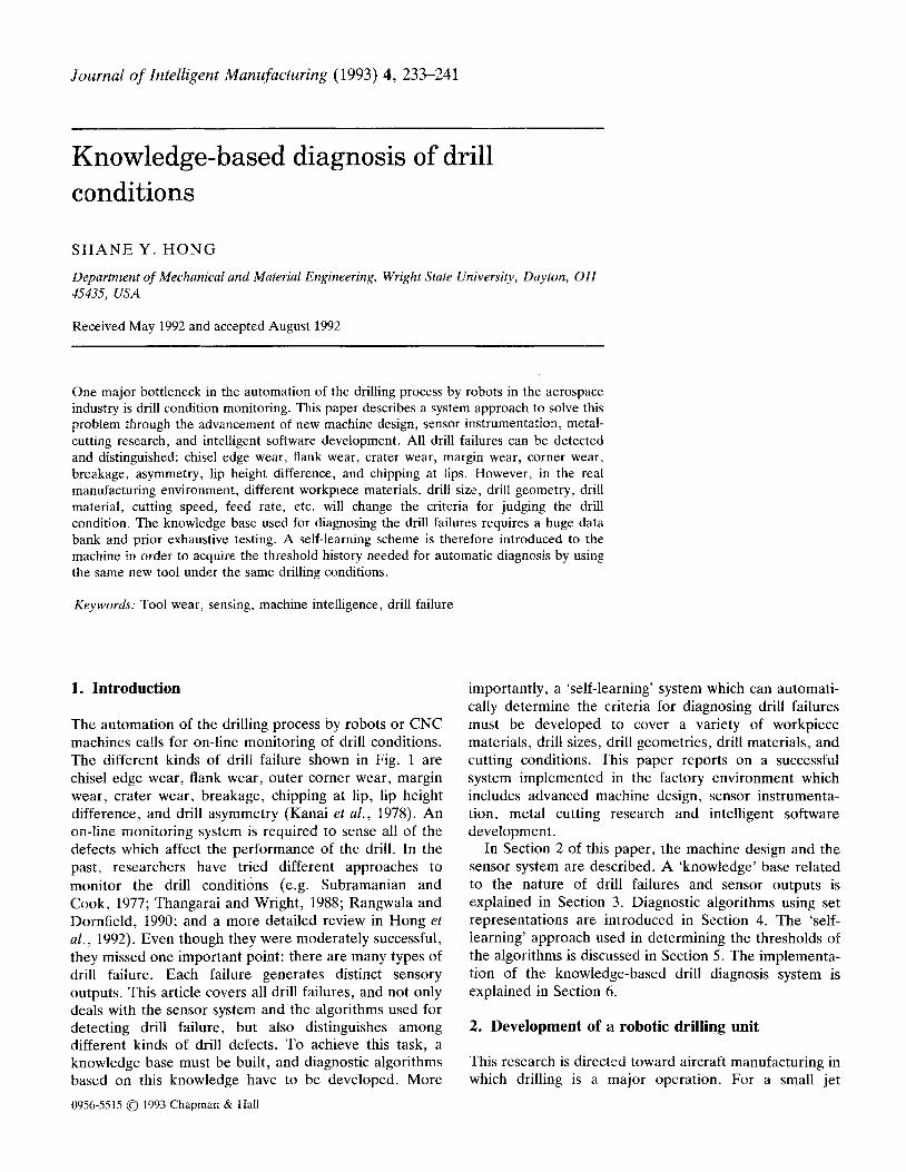
We start off with any ordinary amplifier, represented by the dotted box in Fig. I. We know that when we apply a certain signal voltage to its input we get a certain signal voltage at the output. For convenience let us call these voltages 'Vi and v0 respectively . Then v0/vi is the voltage amplification ; let us denote it bv A.
Negative,
feedback is next applied; in this
What I want to emphasize is that in any inquiry into negative feedback it is fatal to use the external input, Vi, as the starting point . Always begin with 'Vi or v0• Then the other (v0 or vi) follows £ro1n ordinary amplifier knowledge, without any feedback complications. And when once you have decided how much of v0 to feed back, Vi is arrived at merely by adding this fed-back voltage to 'V;.
Though
example, by con- r�i:bi_!_E�1 necting part of the f t <>-'------<>
say "merely by adding," I don't mean that it is 1 always just as simple as adding
v0 2 and 3. If it output voltage in :;;!,_ Vit
Au; were, then the
series with the V· ;;;:� input. It is some- 11 �� thing done en- i_ tirely outside the 0-------------0 dotted box ; and
j complications we are about to consider would not arise. The source of all the trouble is what we have denoted by the deceptively simple letter A.3 It is what is known as
so, provided that the load impedance is kept the same, it has no effect on what goes on inside the box. The amplification there is still A,
Fig. 1. In an amplifier using negative feedback, the amplifier proper (within the dotted lines) works quite normally, and the results of the feedback are accounted for by what is done
outside it.
and an input signal of vi volts still delivers an output of v0 volts. In practice, of course, the amplifier and the feedback circuit are both made up into a single unit, represented by the outer box. The dotted line in Fig. 1 is an invisible boundary, and its input �·, terminals" may be merely unmarked points on the wiring.
So the voltage which it is necessary to apply to the external input terminals ·(call it Vi) in order to get v0 at the output is equal to vi plus the fed-back voltage, which is a fraction of v0• If we call this fraction B, then the fed-back voltage is Bv 0, which is equal to
· ABvi.2 So the total external input must be vi + ABvi = vi(I + AB),
• If the whole of v0 is fed back, B - 1.
a vector quantity. That is to say , it doesn't merely denote the number of times the output voltage is greater than the input, but it must also specify the phase of the output relative to the input. One could say, for example, that A was 150, with 30° lag. Another way of presenting this information is by means of a vector in a diagram. Still another -and generally the most convenient-is by the "j " notation, which in this case would be 130 + j75.4
3 Strictly speaking the same complications apply to B too, but they are usually less important there, provided that one sticks to simple resistance feedback circuits and does not try any tricks with inductance or capacitance, to make the feedback depend on frequency.
4 130 and 75 are derived from 150 and 30° in the usual way by multiplying 150 by cos �0° and sin 30° respectively.
190
When Negative Feedback Isn't Negative-The simplest case is the one
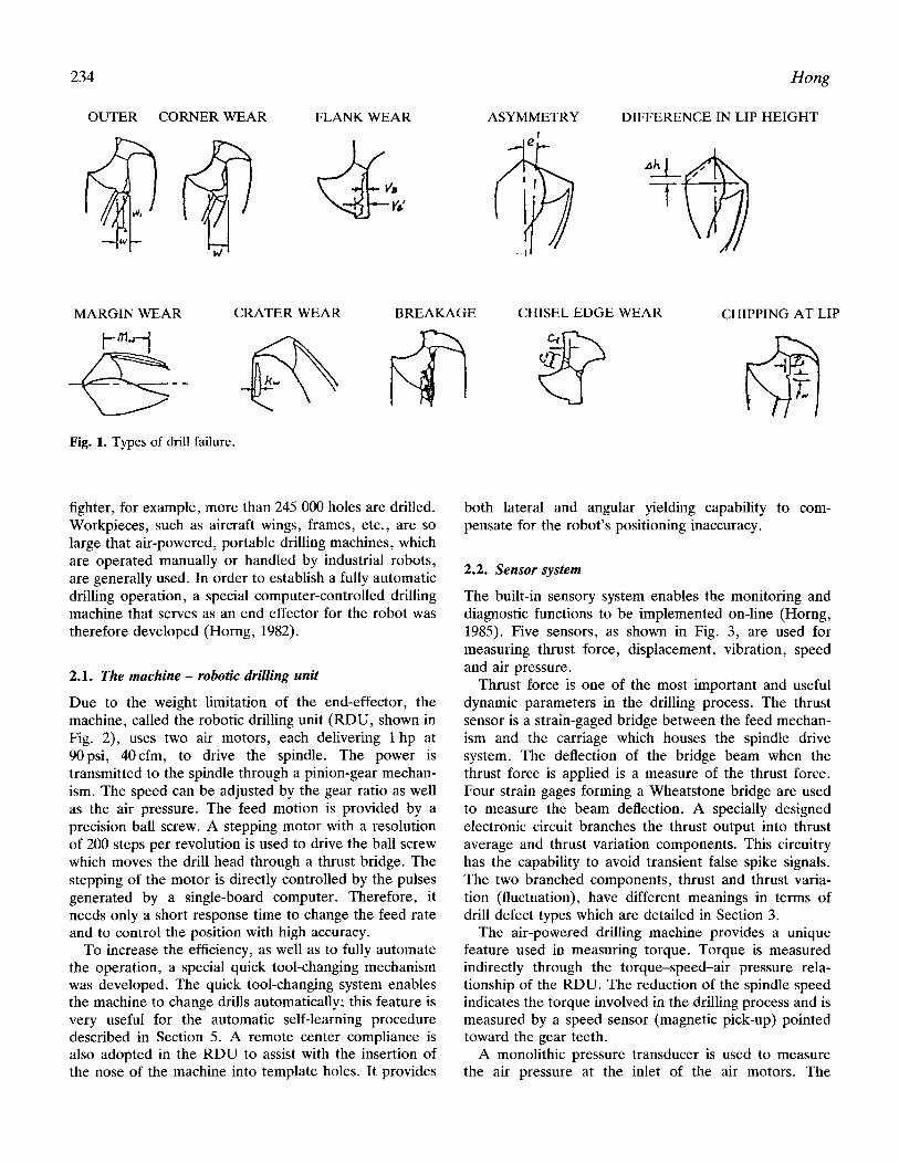
with zero phase difference between output and input voltages, because then the fed-back voltage adds directly to 1•1 to give the input voltage, V;. This can be shown in a simple vector diagram, Fig. 2.
v t
i b Id c
Fig. 2. Vector diagram applying to Fig. I when the output voltage
is in phase with the input.
The vector oa is drawn to represent vi, and oc is drawn A times as long, to represent v0• Being in the same direction, it represents an output exactly in phase with the internal input (vi), such as would be the case with an ideally simple cathode follower or 2-stage resistance-coupled amplifier. ob is then marked off along oc to r�present the'' fed-back fraction, Bv0; the external input, ad, is oa + ob. (In a cathode follower, the whole of the output is fed back, so ob coincides with oc, and the input voltage is greater than the output by the amount 'V;.)
Since in this case all the quantities are in phase, it is much easier to add them by simple arithmetic than to draw a vector diagram. The only purpose of Fig. 2 was to show the principle of the thing, for comparison with other cases. And of course the j method is quite unnecessary in this case, because j indicates the out-of-phase component, which is non-existent.
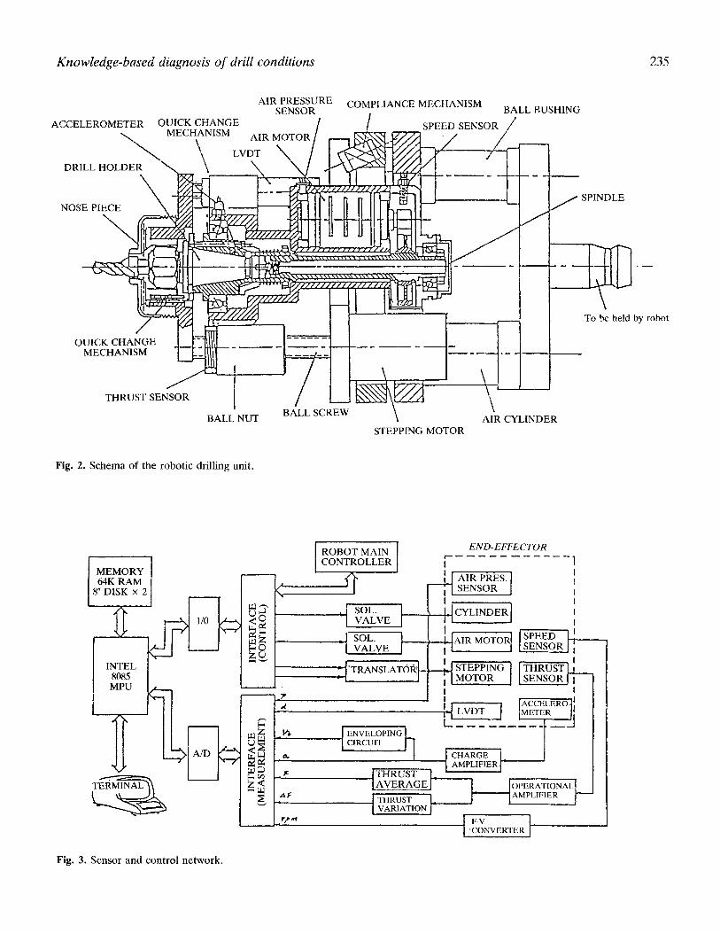
Next, consider a simple resistance-coupled audio amplifier, Fig. 3 (in which provision for grid bias and other details have been omitted for clearness). The only visible components whose behaviour depends on frequency are the coupling capacitors C1 and c., and they are normally chosen so that their reactance at all working frequencies is negligible, in which case the output voltage is in phase with the input and Fig. 2 applies.
At very low frequencies, however, the reactance of C1 is
Wireless Worltl May, 1949
appreciable in comparison with R2, and these two components form a sort of potential-divider. Only part of the output of Vr reaches the input ofV2. What is more, the< current through a capacitor leads the voltage across it by 90'0 ; and, since the voltage across Ri must be in phase with the current through H.2 and C1, the voltages across R2 a nd C1 are 90° out of phase with one another. So when the frequency is low enough for the reactance of cl to be appreciable, not only does the amplification begin to drop, but also the phase of the output starts to lead the input.
As a matter of fact, it is the phase that is the first to start changing noticeably. This doesn't matter in a " straight " amplifier used for listening purposes only, because the ear cannot detect even the maximum phase shift. But if negative feedback is used it does matter. To see how, we must go into the matter more closely.
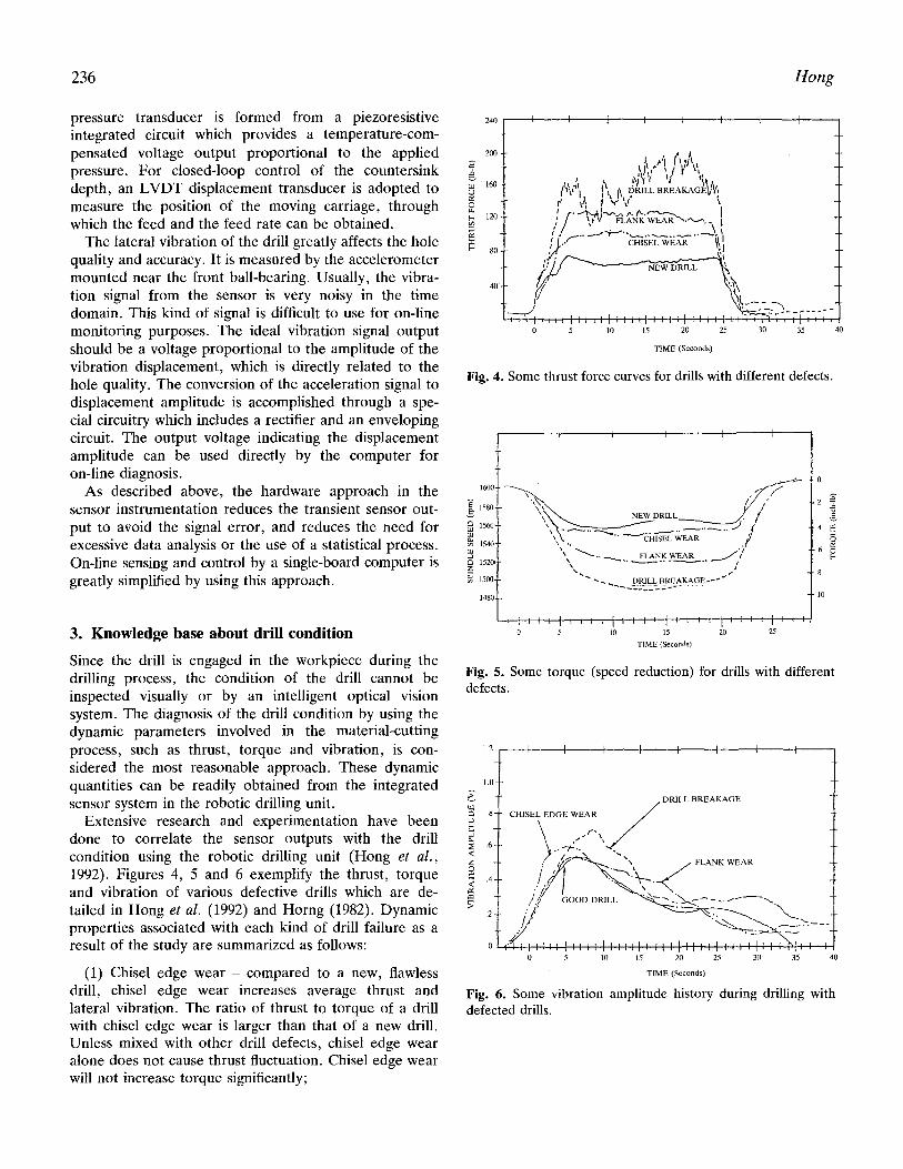
Assume that the signal input to VI can be varied in frequency but is constant in amplitude, yielding a certain output (v al) at the anode. If the resistance R2 is very large compared with R1 and r1a (the anode resistance of Vr), then the additional impedance of cl at very low frequencies will not affect vat appreciably. So we shall assume that v al is constant too, and therefore can be represented - by a vector line of fixed length (oe in Fig. 4).
The voltages across C1 and R2, which we can call v cl and v g2 respectively, can also be represented by vectors, which will have
r t
they differ in pha�e by 90°, their vectors, fe and of in Fig. 4, must always be at right angles to one another.
You can make a working mod.el of this vector diagram under these conditions by sticking pins in the points o and e and pushing the right-angled corner of a card between them, ignoring the part of the card below oe. One e�ge of the card will form the vector of and the ·Other fe.
Except at low frequencies, t4e reactance of cl is so small compared with R2 that the voltage across it (v c1) is negligible ; this condition is represented by holding the card so that its edge of coincides with oe,. and fe disappears. But as the frequency is reduced, v cl correspondingly increases, as can be shown by bringing fe into view, still keeping the card pressed against the pins.
/ I I I
�---/ ' / " / 'f
Fig. 4. Vector diagram applying to the C1R2 portion of Fig. 3 (and also to C3R!), showing how v 02
is. related to Va1
To do this you must turn the card anti-clockwise, so that its edge of indicates a phase-shift, <f>. But at first its length is hardly affected. As vc1 grows,. howi>:ver, v02 dwindles at an mcreasmg rate ; until finally, when v cl becomes relatively large, v u2 rapidly disappears while the angle of phase
difference ap
Ci
proaches 90° quite slowly. The corner of the card (as is proved in geometry) traces out the circumference of a semi-f circle, dotted in Fig. 4. "gz R4 OUTPUT V0 To make the chap_ges in v 0 2 and <P clearer in relation to frequency, t h e y c a n be plotted on a frequency b a s e
LO---�-'---+-------'--t -�--0-1 Fig. 3. The effects of the coupling capacitances, C1 and C3, and the stray capacitances (not shown) in this amplifier cir.cuit are considered in detail.
to fulfil two conditions. The first is that they must of course always add up (vectorially) to equal Vai· And since, as we have just seen,
as in Fig. 5. The frequency scale shown holds good for all combinations of C1 (in µF) and R2 (in MO), which when multiplied
May, i949 \Vireless \Vorld
together are equal to r megohmmicrofarad. For other combinations the shapes of the curves are the same but the ·frequency figures
� 80 � 70 dS- 60 g so .: 40
i 30 2J
,__ __ -"' '
v -DO 01 002
v
o·os
J... / Ug1
J v., /
�' '
0·1
' ',
'
0·2 o·s 1FREQUENCY (c/s)
---
If an amplliier could be made strictly according to Fig. 3 there would be no limit ; but unfortunately there are the " in-
---
I ·o 0·9
v i sib l e c o m p o n e n t s ''-stray capacitances. One lot of these, in
o·a eluding the input 0·1 ?!.>' capacitance of V2 0·6 � 0·5 0:4 � :::; 0·3 � 0 ·1 O·I
10"
and the output capacitance of Vr, comes across R2, so we shall call it C2• B y u s i n g Thevenin's theorem5 we can boil down the parts of the circuit con
Fig. 5. Both .P and v gz in Fig. 4 depend on frequency ; here they are plotted on a frequency
base to bring out this relationship.
cerned to Fig. 6, in which R is equal to I{al• R1
must be divided by the number of megohm-microfarads.
If there is another coupling, C3R4 in Fig. 3, it behaves similarly ; and the combined effect of the two is calculated by adding their individual phase shifts and multiplying amplitude ratios. So the total phase shift due to the two couplings approaches r8o0 lead at the lowest frequencies.
In practical amplifiers this verylow-frequency behaviour is generally a good deal more complicated. Capacitors used for smoothing the main power supply, decoupling individual valve feeds, and bypassing bias resistors, tend to become ineffective ; with the result that the impedances they are supposed to short-circuit cause various positive or negative feedbacks that may do almost anything to the frequency characteristic of the amplifier. The cunning designer can so,metimes turn t!).ese effects to his advantage, as for example in bass-boost circuits; or he may make the capacitances as large as can be afforded, to push the trouble below the lowest working frequency. But, as we shall see, that may not dispose of it.
So much in the meantime for the lpw frequencies; what about the high?
Fig. 6. The effect of stray capacitance in Fig. 3 is made clear with the help of this "equ iva l e n t
circuit."
and H.2 in parallel, fed by a generator giving a constant voltage equal to v av when C2 is removed. This voltage has been marked 1! aio·
Now the only difference between this problem and the one already solved for C1R2 is that the desired v u2 comes across the capacitance instead of the resistance ; so of course one wants this capacitive reactance to be as large as possible relative to R. Tht> appropriate
0 ;
<.:> :5
r:p 0 - 30° -45°
I+-- BANDWIDTH \
-60° -90° FREQUENCY
Fig. 7. Typical frequency characteristic of an amplifier of the Fig. 3 type, without feedback. The cut-off frequencies, which limit the effe,:tive bandwidth, are detemiirted r:by the RC (time.::
constii.nt)''vitlues of the circuit.
vector diagram is like Fig. 4 in reverse. The. frequency curves have the s?:me slfape as those in Fig. 5 exCE'1J� ; �l}at they top are reversed; the amplitude ratio is practically ·;)" until some ,::'fairly high frequeti'C'y, when it begins to fall off, artd at the same time' the phase shift begins to grow-but this time i
_t i.? a lag. As with
C1R2, at the· frequency which 3 " Th6venin's,
p.109 Theorem," :\larch-, 1949,
When Negative Feedback Isn't Negative-:-
makes the reactance equal to the resistance, the phase shift is 45° and the amplitude ratio o. 707 (i.e. 1/y2). Obviously the lower the combined valve and coupling resistance (R) the higher the frequency before the phase begins to shift and amplification falls off.
Putting all this together, then, the frequency characteristic of a resistance-coupled amplifier with one series-C coupling and one shunt-C stray ea pacitance, and leaving out of account any other influences :mch as power-supply impedance, is as shown in Fig. 7. The two curves together specify A; I Al being the symbol for its numerical magnitude alone. The two sloping ends are copied from Fig. 5 and its mirror image, and can be made to apply to any amplifier by placing them so that the points where \A\ has dropped to 0.707 times maximum come where the appropriate resistances and capacitive reactances are equal. The amplifier frequency band is commonly regarded as extending from one of these fre-4 uencies to the other.
One of the objects of negative feedback is the widening of this frequency band. How it does this can be seen from Fig. 2. Let oc represent the wanted output. Then oa represents the input required to give it, with no feedback. Over the fiat-top part of Fig. 7 the length of oa will be constant, corresponding to constant amplifr::ation . But at low or high frequencies, where the amplification falls, the length of oa has to be increased to keep the output constant. For
c •
example, at the marked frequencies, where \Al drops to o. 707 of its maximum, the input voltage must be increased by the factor 1/0.707 = 1.41.
With feedback, a greater input, oa + ob say, is needed, so \Al is low even over the fiat region. But ob, which can be made by far the larger part of oa + ob, is a. constant proportion of oc, so a falling off in the internal gain of the amplifier, which affects oa only, has relatively little effect on the overall gain. '
It must be remembered that the phase is affected too, so at the high frequency end the vector diagram becomes something like Fig . Sa.
Wireles!li World May, 1949
ob is of course unchanged, but oc has been made 1.41 times longer and given the corresponding phase lag of 45°. The required input, given by vectorially adding ob and oc, is ad, which is much less than 1.41 times longer than ob, and also its angle of lag is much smaller than rf>. The more negative feedback is used, the less is the phase shift and drop in amplification due to whatever oc does.
So the effects of negative feedback on the frequency characteristic, Fig. 7, are : (1) The fiat top is lowered (from A to A/ (r + AB), as we saw at the beginning) ; (2) the fall-off at each end is less pronounced ; (3) the phase shift at each end is less. But the benefits (2) and (3), can't last for ever as the frequency is raised. In the end the internal input, represented by the vector oc, must become large-even larger than ob-and
� = 450 b o-.:t"/"'::::'::::::::::::�·����--+•a �- -------� (a) b
( b)
' a (c)
d b w �== 180°
.. (d)
•a
Fig. 8. Vector diagrams showing · various conditions in amplifiers
with feedback. The vectors represent the same voltages as in
Fig. 2.
at the same time it swings round nearly at right angles to ob, Fig. S(b). So finally the amplification and phase suffer almost as badly as they did (at some lower frequency) without feedback. Similarly, at the lowfrequency ·end. , With an amplifier that includes
within the feedback loop two RC circuits of the same tendencv, the vector oc grows twice as faS't,
and its phase shift approaches r8o0• This is where things begin to get interesting. Fig. S (c) , for example, shows the condition where each of two similar RC circuits is giving a lag of 60° and from Fig. 5 it can be ascertained that the relative amplification is 0.5 X 0.5, so oc must be four times as long as in Fig. 2. In spite of this, ad is actually shorter than in Fig. 2, so the overall gain is higher. (This assumes, of course, that the amplifier can handle the internal input without being overloaded ; if not, distortion may be violent). So instead of the overall amplification falling off, as it would with no negative feedback, it rises. This can't go on, though ; as </> approaches 90° per RC circuit the internal amplification drops off so rapidly that oc becomes immense, and ad likewise.
But now consider what may happen with three similar RC circuits. At the frequency where each introduces a lag of 60°, the total lag is 180°. And if oa in Fig. 2 was one-eighth of ob, it is now equal to it, so we get the result shown in Fig. 8(d), where ad has shrunk to nothing. In other words, the amplifier will give output at this frequency without any input at all. In still other words, it is selfoscillating.
The same thing is liable to happen at a frequency lower than the working range, if there are three RC circuits of the series-C type.
At first it might seem a very unlikely coincidence that oc would be exactly equal to ob when q, was exactly 180°, and so the risk of oscillation would be small. But this is not so. Make oc in Fig. S(d) any length you like, less than ob. Then the external input, ad, must be in phase with ob. So if ad is reduced, say to zero by shorting the external input terminals oc must increase correspondingly to preserve the balance. But that makes oa and consequently ad increase, so oc must increase more. And so on, until the amplifier is overloaded and its amplification reduced to the point at which ob = oc and oscillation is maintained at a steady amplitude.
Vve have just found that if an
May, 1949 Wireless Worlll
amplifier circuit embraced b:· a negative feedback loop contains three similar RC circuits there will be oscillation unless AB is less than 8. (By " similar " I mean having the s3.me RC; values and tending to cut frequencies at the same end.) With four such circuits the critical phase shift in each is only 45° and the ratio in each (see Fig. 5 again) is o. 707, so the oscillation value of AB is only r/0.7074 = 4. But
back over only one stage, including no transfornwr. But one stage with heayy feedback gives hardly any amplification. Two stages, again with no transformer, offer more useful possibilities, without risk of oscillation, but can develop peaks. ls it possible to include more than two phaseshifting circuits (counting one transformer as two circuits), to combine high amplification with a full measure of the benefits of
we can easily see :z: negative fccd-from the diagrams 0 jj'-\ back ? If one that even if feed- -;��; a d o p t s w h a t back is kept well
::: would normally be
below these fatal L-------------- a sound economic-figures it may still al principle - to be enough to raise FREQUENCY design each stage peaks, as in Fig. Fig. 9. Typical effect of applying to cover the same 9; and these may negative feedback to an amplifier frequency bandcause things like having more than one circuit the answer would cutting off at about the same g r a m o p h o n c frequency. be No. But if you scratch and motor try combining the rumbles to be brought into un- effects of circuits having different desirable prominence. cut-off frequencies you will find
If a transformer is included in that more feedback can be used the system, the danger is greater, at least at the high-frequency end. As is explained in the books, at high frequencies a transformer usually becomes approximately equivalent to a series resonant circuit, composed of the leakage inductance and the stray capacitance. A feature of such a circuit is that the phase angle between the output (across the capacitance) and the input (across the whole) swings from a small lag below the resonant frequency, to 90° at resonance, and approaches 180° , above resonance. So feedback across one transformer and one RC circuit can easily cause highfrequency oscillation.
It can be shown that at the low-frequency end the transformer is roughly equivalent to one RC circuit.
To make an extremely stable and level amplifier it is necessary to use a lot of feedback. Yet, paradoxicaily, in using it one seems certain to run a serious risk of causing oscillation and peakiness. The advi�e one usually gets about this is to see to it that the amplification has fallen well below the danger point at the frequencies where the phase shift is 180°. But, as we have seen in arriving at Fig. 5, the drop and the shift are bound together by the nature of the circuit.
One line of policy is to feed
before peaks appear. In particular, if three shunt-C circuits arc included, as there usuallv will be in three stages, it is best to make one of them cover a narrower frequenc,� band than the other two.
·· ·
The truth of this can be shown in a more professional manner by the "j" method; and anybody who wants to go into the matter more deeply is advised to consult an article by C. F. Brockelsby in the March 1949 Wireless Engineer. He shows how one can design for "maximal flatness," which means "staggering" the cut-off frequencies of the circuits so that feedback can be used to extend the frequency coverage as far as possible, just short of allowing peaks to appear. The tendency to peak, controlled in this way, is useful for squaring the shoulders of the amplification/ frequency curve, without going so far as the curve of Fig. 9.
If your amplifier gives trouble when you feed back over three stages, then try using a low anode coupling resistance for the middle stage and higher values for the two outer ones. Or, if a transformer is included, make sure that the other circuits cut off at a higher frequency. Of course, it is best to work out the design fully and check by tests ; but the foregoing trial-and-error hints are better than nothing.
193