Embed Size (px)
Citation preview
When Failure Analysis Meets Side-ChannelAttacks
Jerome Di-Battista1,2, Jean-Christophe Courrege1, Bruno Rouzeyre2, LionelTorres2, and Philippe Perdu3
1 Thales Information Systems Security,18 Avenue Edouard Belin, 31400 Toulouse, France
[email protected],2 Universite de Montpellier, Laboratoire du LIRMM,
161 rue Ada, 34095 Montpellier Cedex 5, France3 Centre National d’Etudes Spatiales CNES,
18 Avenue Edouard Belin, 31400 Toulouse, France
Abstract. The purpose of failure analysis is to locate the source of adefect in order to characterize it, using different techniques (laser stim-ulation, light emission, electromagnetic emission...). Moreover, the aimof vulnerability analysis, and particularly side-channel analysis, is to ob-serve and collect various leakages information of an integrated circuit(power consumption, electromagnetic emission ...) in order to extractsensitive data. Although these two activities appear to be distincted, theyhave in common the observation and extraction of information about acircuit behavior. The purpose of this paper is to explain how and whythese activities should be combined. Firstly it is shown that the leak-age due to the light emitted during normal operation of a CMOS circuitcan be used to set up an attack based on the DPA/DEMA technique.Then a second method based on laser stimulation is presented, improv-ing the ”traditional” attacks by injecting a photocurrent, which resultsin a punctual increase of the power consumption of a circuit. These tech-niques are demonstrated on an FPGA device.
Keywords: Side-channel, Failure analysis, Light emission, Laser stim-ulation, FPGA
1 Introduction
During the last 20 years, failure analysis has become a serious concern for theelectronics industry. Its purpose is to locate the source of a defect in order tocharacterize it, the defect being a problem linked to the environemental condi-tions, an intrinsic problem in the circuit, or both. More generally, failure analysisshould ensure that the detected problem does not occur again [1]. The strongestconstraints are the size reduction for CMOS technology components and the in-creasing complexity of integrated chips (several millions of gates). Currently themost used analysis tools are based on laser stimulation and light emission tech-niques. Concurrently, during the last 10 years, non-invasive and semi-invasive
techniques have received a lot of attention from the hardware security commu-nity. Among them, so-called side-channel attacks are the most popular. Differentleakage sources [2][3] such as power consumption, electromagnetic field, or timeresponse of the circuit, are correlated to the processed data. Thus, by inspectingthis information, and with the help of appropriate software tools, it is possibleto retrieve the secret data used in the embedded cryptography circuits, typicallythe cipher key. From an attacker point of view, side-channel attacks presentmany advantages, as most of them require only low-cost instrumentations, andthey are non-destructive.
These two activites apparently different can be combined. Indeed, the failureanalysis techniques can be used to extract another kind of side-channel signalor to improve existing side-channel attacks. Inversely, the vulnerability analysiscan be used to extract complementary information about the circuit behavior.In this paper two examples of application, light emission and laser stimulation,are presented.
The light emission phenomenon has been mainly studied for failure analysis.Many techniques have been developed to extract and process the light emittedby the electronic components in order to localize different kinds of defects [4](junction avalanche, oxide breakdown...). In this paper we mainly focus on thelight emitted by NMOS transistors during commutation. Indeed, in [5], the au-thor demonstrates the possibililty to set up an attack based on light emission,by implementing part of an AES algorithm on a PIC16F84A microcontrollerpreviously opened from the backside. The purpose of this attack was to recoverthe secret key stored in the microcontroller RAM. Using this work as a startingpoint, two approaches have been developed; in [6] the author demonstrates thepossibility of using a low-cost system to perform the same kind of experimentson a PIC16F628 and provides some interesting results for a FPGA circuit. Inparrallel, we had chosen to study the Time Resolved Emission (TRE) techniquewhich allows us to count the number of photons emitted by a transistor or by agroup of transistors as a function of time, implemented on a more expensive fail-ure analysis equipment [7]. Our purpose is to show that the extracted TRE signalcan be used to gather sensitive data, such as a side-channel signal, exploitableby a statistical post-processing method (e.g. DPA or CPA).
In the same way as light emission, the techniques based on laser stimulationhave been mainly developed in failure analysis [8][9]. On the one hand, the laserstimulation at a 1064 nm wavelength allows to induce a local photocurrent [10],either to detect a latch-up mechanism and inter-level shorts or to locate opencircuits and direct semiconductor damage (LIVA, OBIC). On the other hand, thelaser stimulation at a 1340 nm wavelength can also induce a thermal variation todetect a resistance variation by measuring the power consumption across a circuit(TIVA, OBIRCH). In [11], the author demonstrates the possibility to increasethe consumption of a SRAM cell transistors in a microcontroller by applying aphotocurrent (639 nm laser). Starting from these experiments, we studied thepossibility to use this method to improve a side-channel attack, by reducing thenumber of power consumption curves necessary to perform the attack.

We experimented both methods on an FPGA Actel Proasic3 A3PE600 inflash technology (0.13µm, 7 metal layers, 600k system gates, single chip). Thistype of circuit offers a very high flexibility, as it is completely customizable, re-configurable and non-volatile. These particularities make the FPGA a good testsample to be analysed on different testing or failure analysis equipments. How-ever FPGAs make the analysis more difficult than ASICs, as the regular structureof FPGA logic elements does not permit to localize sensitive components suchas SRAMs or EEPROMs (by using for instance an optical microscope). Further-more, the attacked microchip is in 0.13µm technology, which may complicate themeasurements due to lower power supply and light emission. To overcome thisproblem, the acquisitions have to be performed from the backside of the chip,even though this requires a more sophisticated sample preparation [12].
2 Light Emission as a Side-Channel Signal
2.1 Background
Currently, most digital circuits are based on CMOS technology. One of the par-ticularities of CMOS transistors is that photons are emitted during their com-mutation. Indeed when a current flows between the source and the drain, theelectrons gain energy and accelerate due to the electrical field. The radiative ”de-excitation” of the charge carriers in the pinch-off zone generates photons whichare visible in the near-infrared spectral range [13]. This emission is predominantfor a transition from 0 to 1. For a 1 to 0 transition the emission is usually toolow to be acquired. This phenomenon produces an asymmetric light emissionprofile for the two transition types (0 to 1 and 1 to 0). This asymmetry can thenbe used to extract relevant information from the circuit.
To observe the light emitted, the chip needs to be opened either from itsbackside or frontside, depending on its package type. Furthermore, the lightemission quality depends on the quality of the package opening process [14]. Forthe backside package opening, the silicon substrate is mechanically thinned downand polished. Indeed the thinning is necessary to decrease the absorption rateof the silicon substrate, and also to maximize the generation of photocarriers inthe silicon [15]. On the other hand, when working on the frontside, a chemicalprocess is used, which is easier to perform. Nevertheless, because of the increasingnumber of metal layers in the circuits that act as a light screen, this techniqueis less and less used.
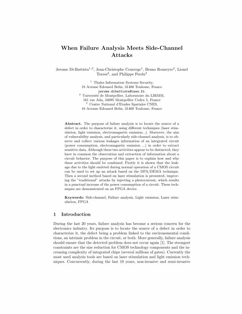
The photons emitted can be collected by a specific device equipped with ahigh sensitivity photon sensor mounted on the optical axis of a conventionalmicroscope. Many types of optical sensors, working with different wavelengthefficiencies, can be used (CCD, InGaAs, InSb...). However, due to small transistorsize and high silicon doping in the most recent technologies, at normal powersupply voltage, the photon emission is maximum in the 900 nm - 1100 nmrange. In this spectral range InGaAs detectors have the best quantum efficiency,as shown in Fig.1.
Fig. 1. Comparison of sensor technologies in relation to the silicon transmittance: re-sponse as a function of wavelength
In order to perform our experiments we identified two main complementarytechniques able to produce time and spatial information: the Picosecond ImagingCircuit Analysis (PICA) and TRE techniques.
The PICA system acquires the light emitted, conserving time and spaceinformation. More precisely, the PICA sensor delivers the time and positionof each photon emitted by the targeted circuit zone [16]. This technique hasbeen initially developed to identify any functionality problem using temporalinformation during backside inspections [17].
The PICA system can be coupled with the TRE technique to target a singletransistor or a specific zone in the circuit under inspection. The TRE can producean histogram of the number of photons emitted as a function of time [18]. Thesehistograms are called ”TRE curves” and are shown in Fig.4.
2.2 Experimental Method
Since the light emitted depends on the operation executed, there is a straightcorrelation between TRE waveforms and the cryptographic calculations. Thiscorrelation can be exploited through a DPA process. The aim of the DPA isto reveal the secret keys of cryptographic devices based on a large number ofpower consumption traces that have been recorded during the data encryptionof a cipher algorithm. The main advantage of this process is that it only requiresknowledge of the cryptographic algorithm that is executed [2]. After extraction ofpart of a sub-key, the missing parts can be gathered by iterating the process. Forour purpose, we replaced the power consumption acquisitions by light emissiontraces (TRE).
The acquisition system used is a Hamamatsu Tri-PHEMOS equipment [19].This equipment is composed of an InGaAs camera coupled with a photon count-ing system. Thanks to this apparatus, we were able to carry out a successfullmeasurement campaign using a Hamamatsu high performance InGaAs camera

(high infrared sensitivity in the 950 nm to 1400 nm range). The optical sensorof the InGaAs camera (resolution of 640x480 with a pixel size of 20µm x 20µm)associated with a Solid Immersion Lens (SIL) allows to obtain a resolution of300 nm and to observe a structure on a 65 nm chip. Moreover, the Tri-PHEMOSequipment is able to perform both static and dynamic light emission measure-ments with very high precision.
For the experiment we choose to implement part of a cipher algorithm ona FPGA device as shown in Fig.2. A specific test board was built, as shown inFig.3. It is composed of a FPGA mechanically opened from the backside (silicons down to 70µm), and laid upside down. In addition, a built-in potentiometercan be used to increase the FPGA core voltage (1.5V to 3V) in order to increasethe light emission activity. In this experiment we performed the measurementsat the typical voltage level (1.5V).
Fig. 2. Different view and informations about the FPGA Actel Proasic3e a) x-rayimage b) Picture of the FPGA open from the backside c) Layout informations [20]with location of the DES implementation
The target of our attack was a fragment of a Data Encryption Standard(DES) cipher algorithm. Indeed, in order to simplify our experiment and lightenthe data processing, the chosen target was the first round of the DES algorithm,and more specifically the first SBOX. Our goal was to validate the theory andthe method efficiency on a small part of the DES algorithm.
Prior to these acquisitions, the light emission activity induced by the ’cryp-toprocessor’ needs to be localized in order to start the acquisition. This is doneby a static scan, consisting in acquiring the light emitted for a few minutes inorder to obtain a photon cartography of the whole FPGA. During this time,the cryptoprocessor encrypts the same message. Then the acquisition windowis placed on the emissive area of the cryptoprocessor. Indeed, one asset of this

Fig. 3. FPGA test board
method is that, if the cryptoprocessor can be turn on/off it can be easy to locatethe area where it is implemented. The most relevent point is that it is usuallysufficient to know the location of the cipher block in order to position a TREaquisition window on it. Furthermore, it is not necessary to know either the ar-chitecture of the algorithm, or its implementation, as the overall light emissionof the cipher block is collected instead of a specific area (SBOX output, XORoperation...). It is then the data post-treatment on the TRE curves which willgive us the expected results.
2.3 Results
In Fig.4 the light emission activity of the area where the cipher algorithm isimplemented and the corresponding TRE curves are shown. A first message M1(Fig.4a) is sent to the algorithm, followed by a second M2 (Fig.4b). We cannotice that the variation of the input vector sent to the cipher algorithm gen-erates a time and space variation of the emitted light, producing some sensitivedifferences between the TRE curves. In this way we obtain a TRE curve for eachcryptographic calculation, which can then be used as a side-channel signal.
The full set of message vectors (26 = 64) is sent to the device. In order toobtain the TRE curves, each of the vectors is sent at a frequency of 10MHzduring 20 seconds, also it has been verified that 5 seconds are sufficient. Weused a longer acquisition time to ensure that the camera acquired a number ofphotons high enough to generate meaningful TRE curves. Each vector is sent tothe FPGA in alternance with a zero message. This alternation is needed to forcethe transisitors to reset. When reseted transistors switch to 1, light emissionhappens; therefore reseting the transistors force them to emit light. This processgenerates a set of 64 TRE curves.

Fig. 4. Variation of TRE curves in function of the light emission activity
Once the TRE curves are acquired, it becomes possible to process them inorder to try to extract the key. In our case, the chosen discriminant to classifythe curves in the transition groups (0 to 1 or 0 to 0) is based on the chosenbit at the SBOX output, since during the acquisition we forced a reset betweeneach message by sending a zero value. The differential curves resulting from thestatistical processing on each output bit are shown in Fig.5.
Fig. 5. Differential curves of the 64 key hypothesis for each output bit (number ofphotons emitted as a function of time(µs))

The attack performed on the third bit reveals the right key; however, theattacks on the first, second and fourth bits are inconclusive. On the other hand, ifwe sum up the four output bits to enhance the differences between the differentialcurves [21] we obtain the results shown in Fig.6. These results show that thecurve for the right sub-key stands out. This result demonstrate, by targeting thewhole cipher block with a TRE acquisition window (without a real precision),the possibility to exctract a sub-key by using light emission leakage. In the nextsection, we propose to demonstrate that laser stimulation coupled with the DPAmethod could be an innovative technique for side-channel analysis.
Fig. 6. Sum of differential curves for each output bit (number of photons emitted as afunction of time(µs))
3 Laser Stimulation To Improve side-channel Attacks
3.1 Background
The photoelectric laser stimulation is a failure analysis technique that uses ascanning laser beam to induce a current flow. This one can be collected andanalyzed to generate images that represent the semiconductor sample properties[10]. Indeed, when the laser beam scans the surface of the sample, some electronsinto the conduction band are excited thanks to the ’single-photon absorption’phenomenon. In the single-photon absorption process, a single photon excitesone conduction band electron. This can only occur if that single photon carriesenough energy to overcome the band gap of the semiconductor (1.2 eV for Silicon)and provide the electron with enough energy to make it jump into the conductionband. The creation of charge carriers by excitation of the semiconductor with anoptical beam results in a current flow that can be collected and used for imaging.

The IC current variations induced by the laser beam is converted into a contrastvariation to form an image [8].
One limitation of this technique is that for modern integrated circuits, it ishard to transmit light uniformly to the semiconductor itself. This non-uniformtransmission of light is caused by the presence of several metal layers and othermaterials above the semiconductor. In such instances, one solution is to performthe imaging from the backside through the substrate. However the spatial reso-lution is limited due to a compromise between being able to transmit the beamthrough the substrate, and allowing the beam to be absorbed by the semicon-ductor for the generation of electron-hole pairs that are measurable as a current,as shown in Fig.7.
Fig. 7. Absorption coefficient and penetration depth as a function of wavelength [22]
The laser stimulation can be performed by a specific device equipped witha laser beam mounted on the optical axis of a conventional microscope. Twotypes of laser beams, working with different wavelength, can be used: 1064 nmto induce a photocurrent effect and 1360 nm to induce a thermal effect (and asmall photocurrent effect as well). However, the present experiment involves theuse of the photocurrent effect, thus the 1064 nm (or less) wavelength is chosen.
3.2 Experimental Method
The aim of this experiment is to extend the method described by Skorobogatov[11] to a DPA attack on a DES cipher algorithm, implemented on a FPGA.With the help of a scanning laser equipment used in failure analysis activities,it becomes possible to scan a chosen area into the FPGA corresponding to thelocation where a critical function (SBOX, end of round, XOR) of the DES isimplemented. Theoretically, the laser induces a current on the chosen scanningarea. This additional current should increase the consumption of the circuitduring the algorithm encryption, and thus improve the attack by reducing thenumber of power consumption acquisitions.

The light source used is the Meridian I acquisition system from DCG Sys-tems [23], equipped with a laser scanning microscope system (LSM) with twodifferent lasers for induced current and thermal stimulation (1064 nm and 1340nm). For the experiment, we implemented a full DES cipher algorithm on thesame FPGA device (Actel Proasic3) as for the light emission experiment. ThisFPGA is opened from the backside and mounted on the same specific test board.The main interest of the FPGA implementation is that it is possible to choosethe area where the different DES sub-blocks are implemented on the FPGAprogrammation grid, as shown in Fig.8.
Fig. 8. Location of the DES SBOX on the FPGA programmation grid
The first challenge is the choice of the power laser source, since it is necessaryto ensure that the power is neither too low to generate enough photocurrent nor,too strong to avoid a fault injection. For the considerate wavelength, several testsrevealed that the maximum power at which the algorithm generates errors is 15-18 mW, therefore a laser power of 10-11 mW is chosen. The second challenge isto select an area for the laser scan, for instance SBOX area. After several trialswe selected the area including the 4th, 7th and 8th SBOX (dotted in Fig.8),offering the possibility to scan three SBOX at the same time with a 1µm laserspot size at 20x zoom lens. Once these steps are complete, a first DPA attackis performed without any laser scan in order to have a reference, followed by asecond DPA attack with the laser scan on the area previously identified.

3.3 Results
During the first acquisition process, without any scanning laser, 16000 randommessages are sent. The differential process results, considerate as a reference,are shown in the table in Fig.9. The table details the attack results on each bitof each SBOX. The discriminant used is on the one hand a DPA chosen bit atthe End of Round (first four rows), and on the other hand a CPA [24] HammingWeight at the End of round (last row).
Fig. 9. DPA result laser stimulation at the end of the round without (16000 curves)
A second acquisition process with a scanning laser (with a scan frequencyof 200 khz) is then performed, with the same random messages. In Fig.10 thetable shows the comparison between the numbers of power traces necessary toperform the attack with and without the laser scan. The discriminant used isagain a DPA chosen bit at the End of Round (first eight columns), or a CPAHamming Weight at the End of round (last two columns). In each case thenumber of curves necessary to obtain the right sub-key is shown.
Fig. 10. Comparison between both DPA results with and without laser stimulationand numbers of curves necessary to perform the attack - (laser 1064 nm / power 11mW

These results highlight several interesting facts. First, the number of curvesrequired to perform a successfull attack are decreased by approximately halfon bits (0,1) of SBOX 4 and bits (2,3) of SBOX 7. Moreover, the attack onbits (2,3) of SBOX 4 and bits (0,1) of SBOX 7 with the laser scan allows torecover the good sub-key, whereas the attack on the same bits without laserstimulation are unsuccessful. Likewise, the CPA on SBOX 4 is successful. Theseresults suggest that the laser has a real influence on the power consumptionof the circuits and in particular on the targeted SBOX. Fig.11 highlights theamplitude differences between differential curves with and without a scanninglaser (16000 power consumption curves were used). This comparison underlinesthe influence of laser scans on the efficiency of the attack. Nevertheless the 8thSBOX, although scanned by the laser, is not so impacted (this fact is not yetexplained). On the opposite, bits (0,1,3) of SBOX 6 and bits (0,1) of SBOX 5seems to react to the laser stimulation in a lesser extent. This could be explainedby a spreading of photocurrent neighboring SBOX, or by an indirect influenceof the scanning laser on the interconnection lines between the two SBOX (e.g. 6and 7).
Fig. 11. Amplitude comparison between differential curves on the right key with andwithout laser stimulation (DPA in 16000 curves on bit 0 of SBOX 4)
4 Conclusion
These different experiments show how failure analysis tools could be effectivelyapplied to perform or enhance side-channel attacks. The light emission tech-niques allow to localize the different functions implemented on a circuit. Withonly partial knowledge of the circuit design and by using the TRE technique,
light emission enables determination of the internal behavior of the circuit func-tions. Using the DPA method, we have shown that a differential light emissionanalysis allows retrieval of the cipher sub-key from a fraction of the DES al-gorithm implemented on an FPGA that uses a 130 nm technology. Many de-velopments can be carried out based on this method, and multiple perspectivescan be considered. First, the efficiency of this technique should be compared toother side-channel methods to further highlight the specific contributions of thismethod. Moreover, in the experiments reported here, only time information isused. Space information, which is also available, offers the opportunity to refinethe process and to improve the method. On the other hand, some countermea-sures for this type of attacks have to be developed. A ”natural” one is certainlythe lack of resolution of the sensors versus the latest CMOS technologies (45 nmor less). The light emission profiles are yet to be investigated for these technolo-gies. A countermeasure, for FPGA devices, could be a dynamic reconfigurationto change the light emission profile, or the insertion of sensors inside the packageto detect its opening. We can also notice that the number of TRE curves thatneed to be acquired to break this type of unprotected implementation is muchhigher than those for EMA and DPA.
The second experiment based on a laser stimulation technique allows to par-tially increase the power consumption of a circuit, by scanning a specific areaduring the encryption of the cipher algorithm. This way it is possible to signifi-cantly reduce the number of curves necessary to perform a DPA attack. For thistechnique also many developments and perspective can be considered. These re-cent results require further investigation in order to specify how the laser methodcould be used. For example it could be interesting to repeat several DPA attacksby scanning the SBOX individually (or all the SBOX chained) to establish acomparative statement detailing how the laser method improves the attack. Itwould be also interesting to apply this method on a secure cipher algorithm, forinstance that uses dual rail implementation [25]. Laser scans could be used toinduce an unbalance power consumption and thus exctract the sub-key. Con-cerning the method itself, it would also be interesting to reproduce the attackusing a laser with a wavelength below 1064 nm to increase the photogenerationof free carriers, or to attempt to use other light source (such as halogen light)instead of monowave light laser source. The using of a static laser (without scanmode) to continuously illuminate the area of interest would also be interesting.
The main constraint for these methods is the backside opening of the com-ponent and more particularly the silicon thinning step, a process quite hard tocontrol. In any case, at the present time, due to the price of the equipments usedin these experiments (beyond 2M euros for the Tri-PHEMOS and 500K eurosfor the Meridian), the cost of these attack-enhancing method appears to be veryhigh. An interesting point for future research will be to re-do these experimentson a low-cost sytems to validate the real benefit of them, for example in [6] [11]the author shows the possibility to design a low-cost system based on PMT de-tector coupled with a CCD camera to perform light emission experiments and a639 nm laser coupled with a CCD camera to perform laser experiments. How-

ever, proof that failure analysis and side-channel attacks are compatible has beenprovided, and further studies are currently under way based on these promisingresults.
Acknowledgment
We would like to thank the Hamamatsu Photonics company that allowed us toperform a succesful measurement campaign on their Tri-PHEMOS system, andalso the Hamamatsu team for their technical support. Thanks also to FabienBattistela and Kevin Sanchez for their precious advice and discussions.
References
1. P. Perdu: Contribution a l’Etude et au Developpement de Techniques de Locali-sation de Defauts dans les Circuits Intgrs VLSI, Ph.D. diss., Bordeaux University(2001)
2. P. Kocher, J. Jaffe, and B. Jun: Differential Power Analysis. 19th Annual Interna-tional Cryptology Conference on Advances in Cryptology (CRYPTO’99), LecturesNotes In Computer Sciences ed. Springer-Verlag, vol.1666, 388-397(1999)
3. Jean-Jacques Quisquater, David Samyde: ElectroMagnetic Analysis (EMA): Mea-sures and Counter-Measures for Smart Cards. Smart Card Programming and Secu-rity (E-smart), Cannes, France, LNCS Vol. 2140, Springer-Verlag, 200-210 (2001)
4. D. L. Barton, P. Tangyunyong, J. M. Soden, A. Y. Liang, F. J. Low, A. N. Zaplatin,K. Shivanandan, et G. Donohoe: Infrared Light Emission from Semiconductor De-vices. 22th International Symposium for Testing and Failure Analysis, 9-17 (1996).
5. J. Ferrigno, M. Hlavac: When AES Blinks: Introducing Optical side-channel. IETInformation Security, Vol. 2, No. 3, 94-98 (2008)
6. S. Skorobogatov: Using Optical Emission Analysis for Estimating Contribution toPower Analysis. 6th Workshop on Fault Diagnosis and Tolerance in Cryptography(FDTC). IEEE-CS Press, 111-119 (2009)
7. J. Di-Battista, P. Perdu, J.C. Courrege, B. Rouzeyre, L. Torres, Lionel: Lightemission analysis on FPGA : a new side channel possibility. 7th Workshop onCryptographic Architectures Embedded in Reconfigurable Devices (CryptArchi2009)
8. K.C. Stevens and T.J. Wilson: Locating IC Defects in Process Monitors and TestStructures Using Optical Beam Induced Current. Microelectronic Engineering, Vol.12, 397-404 (1990)
9. G. Soelkner: Optical beam testing and its potential for electronic device charac-terization. Microelectronic Engineering, Vol. 24, 341-353 (1994)
10. J. Fritz and R. Lackman: Optical Beam Induced Currents in MOS Transistors.Microelectronic Engineering, Vol. 12, 381-388 (1990)
11. S. Skorobogatov: Optically Enhanced Position-Locked Power Analysis. Crypto-graphic Hardware and Embedded Systems Workshop (CHES 2006), LNCS 4249,Springer-Verlag, 61-75 (2006)
12. R. Desplats, F. Beaudoin, et Philippe Perdu: Chip Unzip for Backside SamplePreparation. 27th International Symposium for Testing and Failure Analysis, 179-187 (2001)
13. T. Wallinger: Characterization of Device Structure by Spectral Analysis of Photoe-mission. 17th International Symposium for Testing and Failure Analysis, 325-334(1991)
14. D.L. Barton, K. Bernhard-Hofer, et E.I. Cole Jr.: Flip-Chip and Backside tech-niques. Microelectronics Reliability, Vol. 39, 721-730 (1999)
15. F. Baudouin: Localisation de defaut par la face arriere des circuits integres. Ph.D.diss., Bordeaux University, 38-40 (2002)
16. J. C. Tsang, J. A. Kash, D. P. Vallett: Picosecond imaging circuit analysis. IBMJournal of Research and Development, vol. 44, 583-603 (2000)
17. M.K. McManus, J.A. Kash, S.E. Steen, S. Polansky, J.C. Tsang, D.R. Knebel, etW. Huott: PICA : Backside Failure Analysis of CMOS Circuits Using PicosecondImaging Circuit Analysis. Microelectronic Reliability, Vol. 40, 1353-1358 (2000)
18. J. Kolzer, C. Boit, A. Dallmann, G. Deboy, J. Otto, et D. Weinmann: QuantitativeEmission Microscopy. Journal of Applied Physics, Vol. 71, No. 11, R23-R41 (1992)
19. Hamamatsu Photonics: http://www.hamamatsu.com/20. Actel Proasic3 Handbook : http://www.actel.com/products/pa3/docs.aspx, 14421. R. Bevan, E. Knudsen: Ways to Enhance Differential Power Analysis. Lecture
Notes in Computer Science, Springer-Verlag, vol. 2587, 327-342 (2002)22. K. Sanchez: Dveloppement et applications de techniques d’analyse par stimulation
dynamique laser pour la localisation de dfauts et le diagnostic de circuits intgrs.Ph.D. diss., Bordeaux University (2007)
23. DCG systems: http://www.dcgsystems.com/24. E. Brier, C.Clavier, F.Oliver: Correlation Power Analysis with a Leakage Model.
Cryptographic Hardware and Embedded Systems Workshop (CHES 2004), LNCS3156, 16-29 (2004)
25. A. Bystrov, A. Yakovlev, D. Sokolov, and J. Murphy: Design and Analysis of Dual-Rail Circuits for Security Applications. IEEE Transactions on Computers, vol. 54,no. 4, 449460 (2005)


![PRACTICAL ATTACKS ON VOLTE AND VOWIFIVoLTE attacks: The attacks mainly include free data channel, DoS and side-channel attacks on the IMS. Li et al. [5] presents two types of attacks](https://img.pdfslide.us/doc/110x75/5e69e1ab38ce46709e45afcd/practical-attacks-on-volte-and-vowifi-volte-attacks-the-attacks-mainly-include.jpg)