Embed Size (px)
Citation preview
ARM-32 BIT MICROCTROLLER MODULE-1
SIET,ECE DEPT
What Is the ARM Cortex-M3 PROCESSOR?
The microcontroller market is vast, with more than 20 billion devices per year estimated to be
shipped in 2010. A bewildering array of vendors, devices, and architectures is competing in this
market. The requirement for higher performance microcontrollers has been driven globally by the
industry’s changing needs; for example, microcontrollers are required to handle more work
without increasing a product’s frequency or power. In addition, microcontrollers are becoming
increasingly connected, whether by Universal Serial Bus (USB), Ethernet, or wireless radio, and
hence, the processing needed to support these communication channels and advanced peripherals
are growing.
The ARM Cortex™-M3 processor, the first of the Cortex generation of processors released by
ARM in 2006, was primarily designed to target the 32-bit microcontroller market. The CortexM3
processor provides excellent performance at low gate count and comes with many new features
previously available only in high-end processors. The Cortex-M3 addresses the requirements for
the 32-bit embedded processor market in the following ways:
• Greater performance efficiency: allowing more work to be done without increasing the
frequency or power requirements
• Low power consumption: enabling longer battery life, especially critical in portable products
including wireless networking applications.
• Enhanced determinism: guaranteeing that critical tasks and interrupts are serviced as quickly
as possible and in a known number of cycles
• Improved code density: ensuring that code fits in even the smallest memory footprints
• Ease of use: providing easier programmability and debugging for the growing number of 8-bit
and 16-bit users migrating to 32 bits
• Lower cost solutions: reducing 32-bit-based system costs close to those of legacy 8-bit and
16bit devices and enabling low-end, 32-bit microcontrollers to be priced at less than US$1 for
the first time
1
ARM-32 BIT MICROCTROLLER MODULE-1
SIET,ECE DEPT
• Wide choice of development tools: from low-cost or free compilers to full-featured
development suites from many development tool vendors.
Background of ARM and ARM Architecture
ARM was formed in 1990 as Advanced RISC Machines Ltd., a joint venture of Apple Computer,
Acorn Computer Group, and VLSI Technology. In 1991, ARM introduced the ARM6 processor
family, and VLSI became the initial licensee. Subsequently, additional companies, including Texas
Instruments, NEC, Sharp, and ST Microelectronics, licensed the ARM processor designs,
extending the applications of ARM processors into mobile phones, computer hard disks, personal
digital assistants (PDAs), home entertainment systems, and many other consumer products.
2
ARM-32 BIT MICROCTROLLER MODULE-1
SIET,ECE DEPT
Architecture Versions:
Over the years, ARM has continued to develop new processors and system blocks. These include the popular
ARM7TDMI processor and, more recently, the ARM1176TZ(F)-S processor, which is used in high-end
applications such as smart phones. The evolution of features and enhancements to the processors over time
has led to successive versions of the ARM architecture. Note that architecture version numbers are
independent from processor names. For example, the ARM7TDMI processor is based on the ARMv4T
architecture (the T is for Thumb® instruction mode support).
Over the past several years, ARM extended its product portfolio by diversifying its CPU
development, which resulted in the architecture version 7 or v7. In this version, the architecture
design is divided into three profiles:
• The A profile is designed for high-performance open application platforms.
• The R profile is designed for high-end embedded systems in which real-time performance is
needed.
• The M profile is designed for deeply embedded microcontroller-type systems.
• A Profile (ARMv7-A): Application processors which are designed to handle complex
applications such as high-end embedded operating systems (OSs) (e.g., Symbian, Linux, and
Windows Embedded). These processors requiring the highest processing power, virtual
memory system support with memory management units (MMUs), and, optionally, enhanced
Java support and a secure program execution environment. Example products include high-
end mobile phones and electronic wallets for financial transactions. • R Profile (ARMv7-R):
Real-time, high-performance processors targeted primarily at the higher end of the real-time1
market—those applications, such as high-end breaking systems and hard drive controllers, in
which high processing power and high reliability are essential and for which low latency is
important.
• M Profile (ARMv7-M): Processors targeting low-cost applications in which processing
efficiency is important and cost, power consumption, low interrupt latency, and ease of use are
critical, as well as industrial control applications, including real-time control systems.
3
ARM-32 BIT MICROCTROLLER MODULE-1
SIET,ECE DEPT
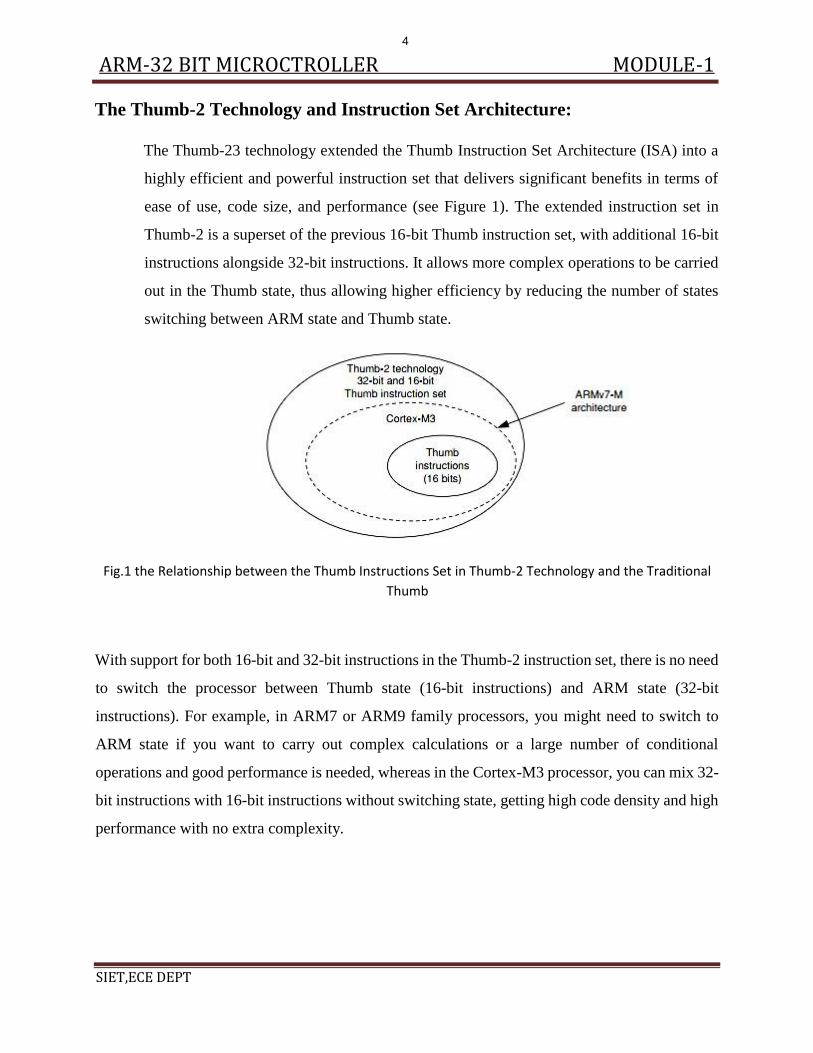
The Thumb-2 Technology and Instruction Set Architecture:
The Thumb-23 technology extended the Thumb Instruction Set Architecture (ISA) into a
highly efficient and powerful instruction set that delivers significant benefits in terms of
ease of use, code size, and performance (see Figure 1). The extended instruction set in
Thumb-2 is a superset of the previous 16-bit Thumb instruction set, with additional 16-bit
instructions alongside 32-bit instructions. It allows more complex operations to be carried
out in the Thumb state, thus allowing higher efficiency by reducing the number of states
switching between ARM state and Thumb state.
Fig.1 the Relationship between the Thumb Instructions Set in Thumb-2 Technology and the Traditional
Thumb
With support for both 16-bit and 32-bit instructions in the Thumb-2 instruction set, there is no need
to switch the processor between Thumb state (16-bit instructions) and ARM state (32-bit
instructions). For example, in ARM7 or ARM9 family processors, you might need to switch to
ARM state if you want to carry out complex calculations or a large number of conditional
operations and good performance is needed, whereas in the Cortex-M3 processor, you can mix 32-
bit instructions with 16-bit instructions without switching state, getting high code density and high
performance with no extra complexity.
4
ARM-32 BIT MICROCTROLLER MODULE-1
SIET,ECE DEPT
Cortex-M3 Processor Applications:
• Low-cost microcontrollers: The Cortex-M3 processor is ideally suited for low-cost
microcontrollers, which are commonly used in consumer products, from toys to electrical
appliances. It is a highly competitive market due to the many well-known 8-bit and 16-bit
microcontroller products on the market. Its lower power, high performance, and ease-ofuse
advantages enable embedded developers to migrate to 32-bit systems and develop products
with the ARM architecture.
• Automotive: Another ideal application for the Cortex-M3 processor is in the automotive
industry. The Cortex-M3 processor has very high-performance efficiency and low interrupt
latency, allowing it to be used in real-time systems. The Cortex-M3 processor supports up
to 240 external vectored interrupts, with a built-in interrupt controller with nested interrupt
supports and an optional MPU, making it ideal for highly integrated and cost-sensitive
automotive applications.
• Data communications: The processor’s low power and high efficiency, coupled with
instructions in Thumb-2 for bit-field manipulation, make the Cortex-M3 ideal for many
communications applications, such as Bluetooth and ZigBee.
• Industrial control: In industrial control applications, simplicity, fast response, and
reliability are key factors. Again, the Cortex-M3 processor’s interrupt feature, low interrupt
latency, and enhanced fault-handling features make it a strong candidate in this area.
• Consumer products: In many consumer products, a high-performance microprocessor (or
several of them) is used. The Cortex-M3 processor, being a small processor, is highly
efficient and low in power and supports an MPU enabling complex software to execute
while providing robust memory protection.
5
ARM-32 BIT MICROCTROLLER MODULE-1
SIET,ECE DEPT
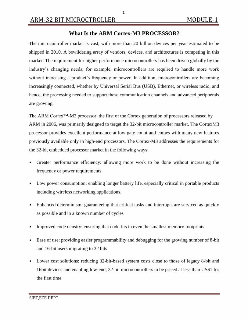
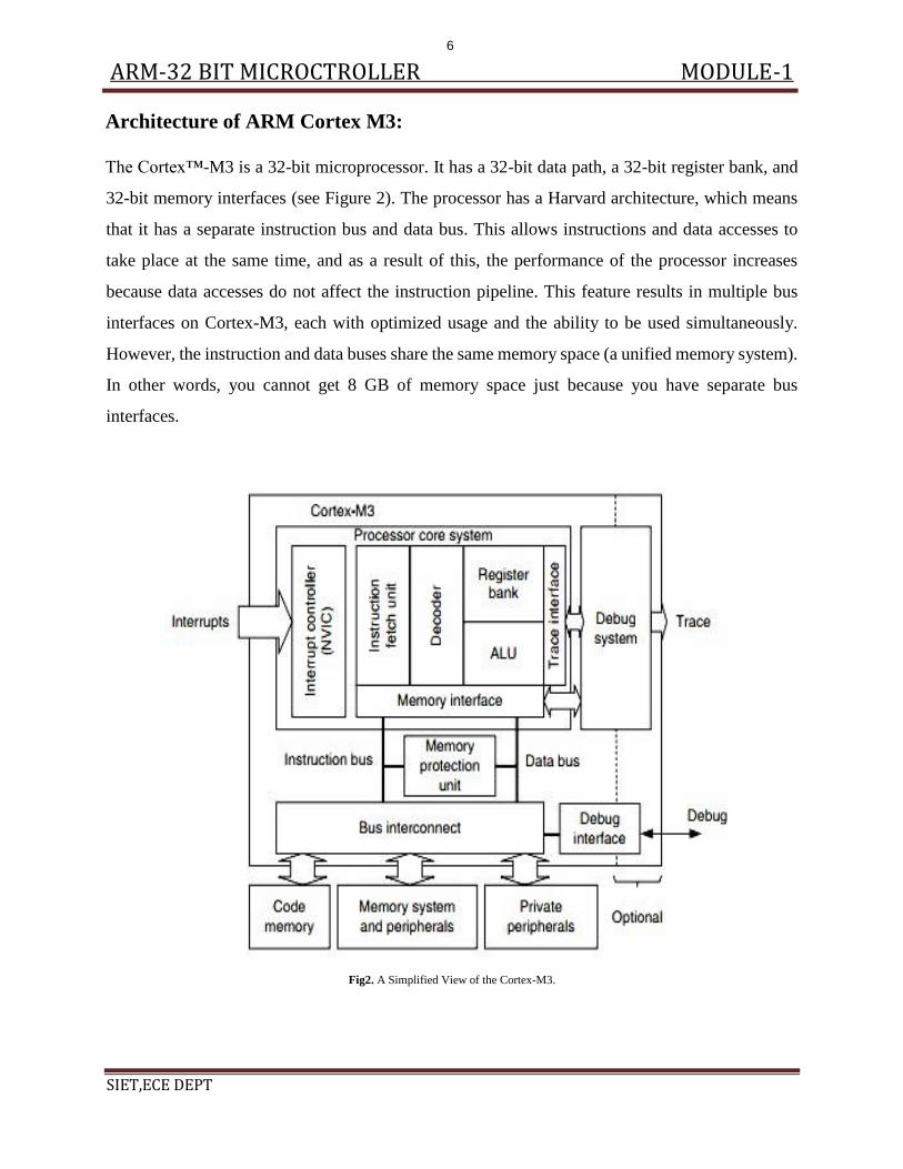
Architecture of ARM Cortex M3:
The Cortex™-M3 is a 32-bit microprocessor. It has a 32-bit data path, a 32-bit register bank, and
32-bit memory interfaces (see Figure 2). The processor has a Harvard architecture, which means
that it has a separate instruction bus and data bus. This allows instructions and data accesses to
take place at the same time, and as a result of this, the performance of the processor increases
because data accesses do not affect the instruction pipeline. This feature results in multiple bus
interfaces on Cortex-M3, each with optimized usage and the ability to be used simultaneously.
However, the instruction and data buses share the same memory space (a unified memory system).
In other words, you cannot get 8 GB of memory space just because you have separate bus
interfaces.
Fig2. A Simplified View of the Cortex-M3.
6
ARM-32 BIT MICROCTROLLER MODULE-1
SIET,ECE DEPT
• The Cortex-M3 processor is a 32-bit processor, with a 32-bit wide data path, register bank
and memory interface. There are 13 general-purpose registers, two stack pointers, a link
register, a program counter and a number of special registers including a program status
register.
• The Cortex-M3 core contains a decoder for traditional Thumb and new Thumb-2
instructions, an advanced ALU with support for hardware multiply and divide, control
logic, and interfaces to the other components of the processor.
• The Cortex-M3 processor is a 32-bit processor, with a 32-bit wide data path, register bank
and memory interface. There are 13 general-purpose registers, two stack pointers, a link
register, a program counter and a number of special registers including a program status
register.
• The Cortex-M3 processor is a memory mapped system with a simple, fixed memory map
for up to 4 gigabytes of addressable memory space with predefined, dedicated addresses
for code (code space), SRAM(memory space), external memories/devices and
internal/external peripherals. There is also a special region to provide for vendor specific
addressability.
• The MPU is an optional component of the Cortex-M3 processor that can improve the
reliability of an embedded system by protecting critical data used by the operating system
from user applications, separating processing tasks by disallowing access to each other's
data, disabling access to memory regions, allowing memory regions to be defined as read-
only and detecting unexpected memory accesses that could potentially break the system.
• The highly configurable NVIC is an integral part of the Cortex-M3 processor and provides
the processor’s outstanding interrupt handling abilities. In its standard implementation it
supplies a NonMaskable Interrupt (NMI) and 32 general purpose physical interrupts with
8 levels of pre-emption priority. It can be configured to anywhere between 1 and 240
physical interrupts with up to 256 levels of priority though simple synthesis choices.
• The debug access into a Cortex-M3 processor based system is through the Debug Access
Port (DAP) that can be implemented as either a Serial Wire Debug Port (SW-DP) for a
two-pin (clock and data) Interface or a Serial Wire JTAG Debug Port (SWJ-DP) that
enables either JTAG or SW protocol to be used. The SWJ-DP defaults to JTAG mode on
7
ARM-32 BIT MICROCTROLLER MODULE-1
SIET,ECE DEPT
power reset and can be made to switch protocols with a specific control sequence provided
by the external debug hardware.
• The Cortex-M3 processor bus matrix connects the processor and debug interface to the external
buses; the 32-bit AMBA® AHB-Lite based ICode, DCode and System interfaces and the 32-bit
AMBA APB™ based Private Peripheral Bus (PPB). The bus matrix also implements unaligned
data accesses and bit banding.
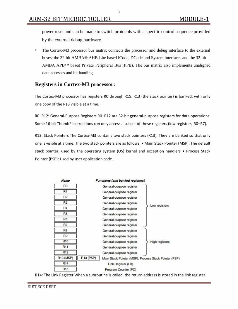
Registers in Cortex-M3 processor:
The Cortex-M3 processor has registers R0 through R15. R13 (the stack pointer) is banked, with only
one copy of the R13 visible at a time.
R0–R12: General-Purpose Registers R0–R12 are 32-bit general-purpose registers for data operations.
Some 16-bit Thumb® instructions can only access a subset of these registers (low registers, R0–R7).
R13: Stack Pointers The Cortex-M3 contains two stack pointers (R13). They are banked so that only
one is visible at a time. The two stack pointers are as follows: • Main Stack Pointer (MSP): The default
stack pointer, used by the operating system (OS) kernel and exception handlers • Process Stack
Pointer (PSP): Used by user application code.
R14: The Link Register When a subroutine is called, the return address is stored in the link register.
8
ARM-32 BIT MICROCTROLLER MODULE-1
SIET,ECE DEPT
R15: The Program Counter The program counter is the current program address. This register can be
written to control the program flow.
Stack Pointer R13
R13 is the stack pointer (SP). In the Cortex-M3 processor, there are two SPs. This duality allows
two separate stack memories to be set up. When using the register name R13, you can only access
the current SP; the other one is inaccessible unless you use special instructions to move to special
register from general-purpose register (MSR) and move special register to generalpurpose register
(MRS).
The two SPs are as follows:
• Main Stack Pointer (MSP) or SP_main in ARM documentation: This is the default SP;
it is used by the operating system (OS) kernel, exception handlers, and all application codes that
require privileged access.
• Process Stack Pointer (PSP) or SP_process in ARM documentation: This is used by the
base-level application code (when not running an exception handler).
9
ARM-32 BIT MICROCTROLLER MODULE-1
SIET,ECE DEPT
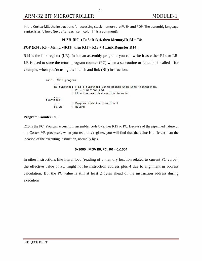
In the Cortex-M3, the instructions for accessing stack memory are PUSH and POP. The assembly language
syntax is as follows (text after each semicolon [;] is a comment):
PUSH {R0} ; R13=R13-4, then Memory[R13] = R0
POP {R0} ; R0 = Memory[R13], then R13 = R13 + 4 Link Register R14:
R14 is the link register (LR). Inside an assembly program, you can write it as either R14 or LR.
LR is used to store the return program counter (PC) when a subroutine or function is called—for
example, when you’re using the branch and link (BL) instruction:
Program Counter R15:
R15 is the PC. You can access it in assembler code by either R15 or PC. Because of the pipelined nature of
the Cortex-M3 processor, when you read this register, you will find that the value is different than the
location of the executing instruction, normally by 4.
0x1000 : MOV R0, PC ; R0 = 0x1004
In other instructions like literal load (reading of a memory location related to current PC value),
the effective value of PC might not be instruction address plus 4 due to alignment in address
calculation. But the PC value is still at least 2 bytes ahead of the instruction address during
execution
10
ARM-32 BIT MICROCTROLLER MODULE-1
SIET,ECE DEPT
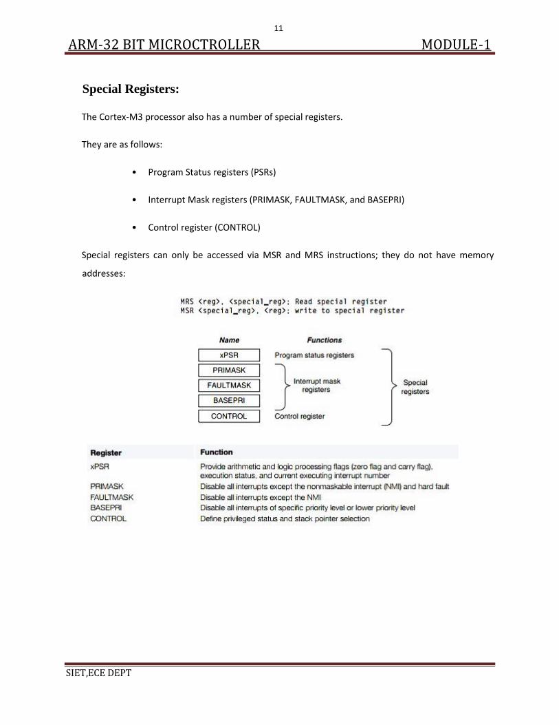
Special Registers:
The Cortex-M3 processor also has a number of special registers.
They are as follows:
• Program Status registers (PSRs)
• Interrupt Mask registers (PRIMASK, FAULTMASK, and BASEPRI)
• Control register (CONTROL)
Special registers can only be accessed via MSR and MRS instructions; they do not have memory
addresses:
11
ARM-32 BIT MICROCTROLLER MODULE-1
SIET,ECE DEPT
The Built-In Nested Vectored Interrupt Controller:
The Cortex-M3 processor includes an interrupt controller called the Nested Vectored Interrupt
Controller (NVIC). It is closely coupled to the processor core and provides a number of features
as follows:
• Nested interrupt support
• Vectored interrupt support
• Dynamic priority changes support
• Reduction of interrupt latency
• Interrupt masking
Nested Interrupt Support: The NVIC provides nested interrupt support. All the external
interrupts and most of the system exceptions can be programmed to different priority levels. When
an interrupt occurs, the NVIC compares the priority of this interrupt to the current running priority
level. If the priority of the new interrupt is higher than the current level, the interrupt handler of
the new interrupt will override the current running task.
Vectored Interrupt Support: The Cortex-M3 processor has vectored interrupt support.
When an interrupt is accepted, the starting address of the interrupt service routine (ISR) is located
from a vector table in memory. There is no need to use software to determine and branch to the
starting address of the ISR. Thus, it takes less time to process the interrupt request.
Dynamic Priority Changes Support: Priority levels of interrupts can be changed by
software during run time. Interrupts that are being serviced are blocked from further activation
until the ISR is completed, so their priority can be changed without risk of accidental reentry.
Reduction of Interrupt Latency: The Cortex-M3 processor also includes a number of advanced
features to lower the interrupt latency. These include automatic saving and restoring some register
contents, reducing delay in switching from one ISR to another, and handling of late arrival
interrupts
12
ARM-32 BIT MICROCTROLLER MODULE-1
SIET,ECE DEPT
Interrupt Masking: Interrupts and system exceptions can be masked based on their priority
level or masked completely using the interrupt masking registers BASEPRI, PRIMASK, and
FAULTMASK. They can be used to ensure that time-critical tasks can be finished on time without
being interrupted.
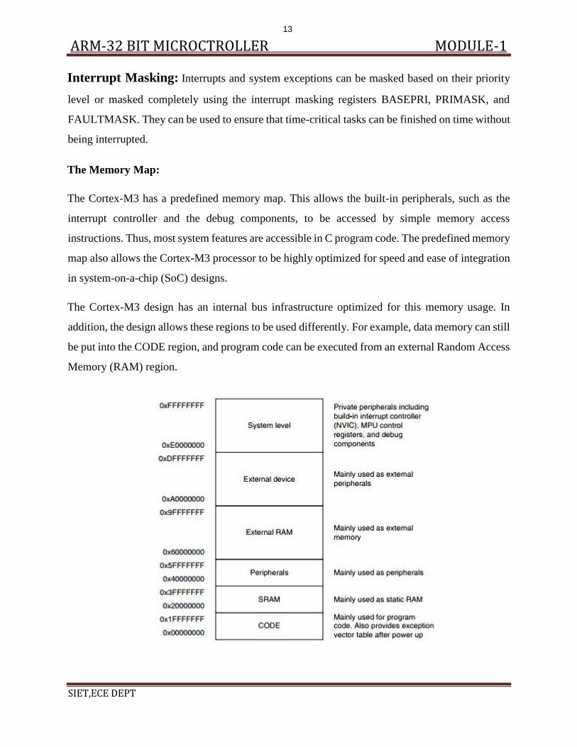
The Memory Map:
The Cortex-M3 has a predefined memory map. This allows the built-in peripherals, such as the
interrupt controller and the debug components, to be accessed by simple memory access
instructions. Thus, most system features are accessible in C program code. The predefined memory
map also allows the Cortex-M3 processor to be highly optimized for speed and ease of integration
in system-on-a-chip (SoC) designs.
The Cortex-M3 design has an internal bus infrastructure optimized for this memory usage. In
addition, the design allows these regions to be used differently. For example, data memory can still
be put into the CODE region, and program code can be executed from an external Random Access
Memory (RAM) region.
13
ARM-32 BIT MICROCTROLLER MODULE-1
SIET,ECE DEPT
The Bus Interface:
There are several bus interfaces on the Cortex-M3 processor. They allow the Cortex-M3 to carry
instruction fetches and data accesses at the same time.
The main bus interfaces are as follows:
• Code memory buses
• System bus
• Private peripheral bus
The code memory region access is carried out on the code memory buses, which physically consist
of two buses, one called I-Code and other called D-Code. These are optimized for instruction
fetches for best instruction execution speed. The system bus is used to access memory and
peripherals. This provides access to the Static Random Access Memory (SRAM), peripherals,
external RAM, external devices, and part of the system level memory regions.
The Instruction Set:
The Cortex-M3 supports the Thumb-2 instruction set. This is one of the most important features
of the Cortex-M3 processor because it allows 32-bit instructions and 16-bit instructions to be used
together for high code density and high efficiency. It is flexible and powerful yet easy to use.
In previous ARM processors, the central processing unit (CPU) had two operation states: a 32bit
ARM state and a 16-bit Thumb state. In the ARM state, the instructions are 32 bits and can execute
all supported instructions with very high performance. In the Thumb state, the instructions are 16
bits, so there is a much higher instruction code density, but the Thumb state does not have all the
functionality of ARM instructions and may require more instructions to complete certain types of
operations.
14
ARM-32 BIT MICROCTROLLER MODULE-1
SIET,ECE DEPT
The Cortex-M3 processor has a number of advantages over traditional ARM processors, such as:
• No state switching overhead, saving both execution time and instruction space
• No need to separate ARM code and Thumb code source files, making software development and
maintenance easier
• It’s easier to get the best efficiency and performance, in turn making it easier to write software,
because there is no need to worry about switching code between ARM and Thumb to try to get
the best density/performance.
The Cortex-M3 processor has a number of interesting and powerful instructions. Here are a few
examples:
• UFBX, BFI, and BFC: Bit field extract, insert, and clear instructions
• UDIV and SDIV: Unsigned and signed divide instructions
• WFE, WFI, and SEV: Wait-For-Event, Wait-For-Interrupts, and Send-Event; these allow the
processor to enter sleep mode and to handle task synchronization on multiprocessor systems
• MSR and MRS: Move to special register from general-purpose register and move special register
to general-purpose register; for access to the special registers.
15
ARM-32 BIT MICROCTROLLER MODULE-1
SIET,ECE DEPT
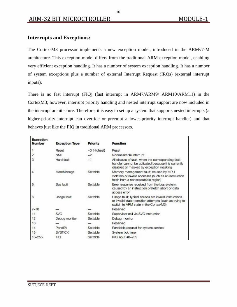
Interrupts and Exceptions:
The Cortex-M3 processor implements a new exception model, introduced in the ARMv7-M
architecture. This exception model differs from the traditional ARM exception model, enabling
very efficient exception handling. It has a number of system exception handling. It has a number
of system exceptions plus a number of external Interrupt Request (IRQs) (external interrupt
inputs).
There is no fast interrupt (FIQ) (fast interrupt in ARM7/ARM9/ ARM10/ARM11) in the
CortexM3; however, interrupt priority handling and nested interrupt support are now included in
the interrupt architecture. Therefore, it is easy to set up a system that supports nested interrupts (a
higher-priority interrupt can override or preempt a lower-priority interrupt handler) and that
behaves just like the FIQ in traditional ARM processors.
16
ARM-32 BIT MICROCTROLLER MODULE-1
SIET,ECE DEPT
Debugging Support:
The Cortex-M3 processor includes a number of debugging features, such as program execution
controls, including halting and stepping, instruction breakpoints, data watchpoints, registers and
memory accesses, profiling, and traces. The debugging hardware of the Cortex-M3 processor is
based on the CoreSight™ architecture.
Unlike traditional ARM processors, the CPU core itself does not have a Joint Test Action Group
(JTAG) interface. Instead, a debug interface module is decoupled from the core, and a bus interface
called the Debug Access Port (DAP) is provided at the core level. Through this bus interface,
external debuggers can access control registers to debug hardware as well as system memory, even
when the processor is running. The control of this bus interface is carried out by a Debug Port (DP)
device.
The DPs currently available are the Serial-Wire JTAG Debug Port (SWJ-DP) (supports the
traditional JTAG protocol as well as the Serial-Wire protocol) or the SW-DP (supports the Serial-
Wire protocol only). A JTAG-DP module from the ARM CoreSight product family can also be
used. Chip manufacturers can choose to attach one of these DP modules to provide the debug
interface.
Chip manufacturers can also include an Embedded Trace Macrocell (ETM) to allow instruction
trace. Trace information is output via the Trace Port Interface Unit (TPIU), and the debug host
(usually a Personal Computer [PC]) can then collect the executed instruction information via
external trace capturing hardware.
17
ARM-32 BIT MICROCTROLLER MODULE-1
SIET,ECE DEPT
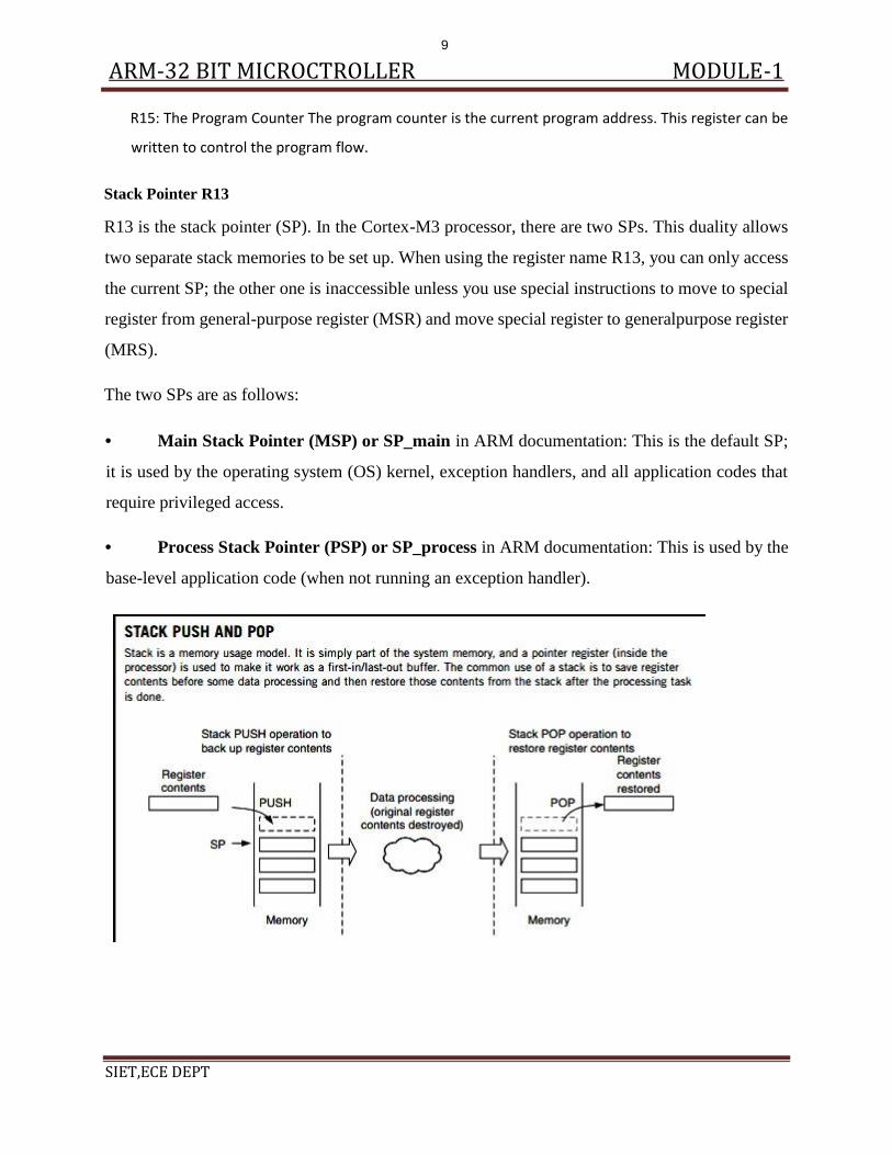
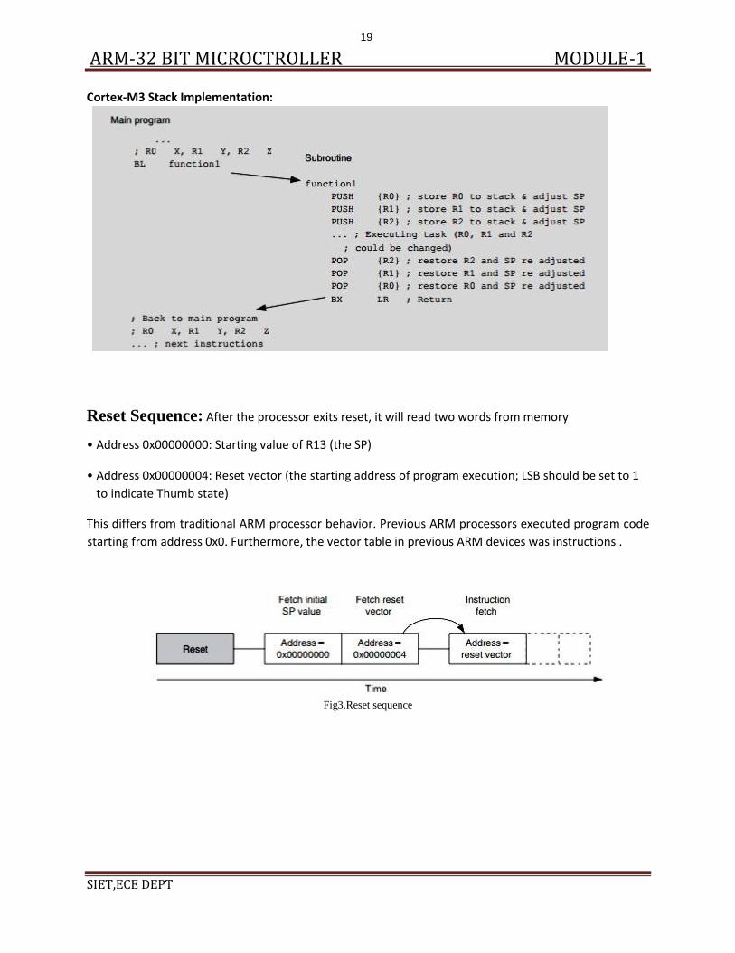
Stack Memory Operations:
In the Cortex-M3, besides normal software-controlled stack PUSH and POP, the stack PUSH and POP
operations are also carried out automatically when entering or exiting an exception/interrupt handler. In
this section, we examine the software stack operations.
Operation:
In general, stack operations are memory write or read operations, with the address specified by an
SP. Data in registers is saved into stack memory by a PUSH operation and can be restored to
registers later by a POP operation. The SP is adjusted automatically in PUSH and POP so that
multiple data PUSH will not cause old stacked data to be erased.
The function of the stack is to store register contents in memory so that they can be restored later,
after a processing task is completed. For normal uses, for each store (PUSH), there must be a
corresponding read (POP), and the address of the POP operation should match that of the PUSH
operation. When PUSH/POP instructions are used, the SP is incremented/decremented
automatically. When program control returns to the main program, the R0–R2 contents are the
same as before.
Notice the order of PUSH and POP: The POP order must be the reverse of PUSH. These operations
can be simplified, thanks to PUSH and POP instructions allowing multiple load and store. In this
case, the ordering of a register POP is automatically reversed by the processor. You can also
combine RETURN with a POP operation. This is done by pushing the LR to the stack and popping
it back to PC at the end of the subroutine.
18
ARM-32 BIT MICROCTROLLER MODULE-1
SIET,ECE DEPT
Cortex-M3 Stack Implementation:
Reset Sequence: After the processor exits reset, it will read two words from memory
• Address 0x00000000: Starting value of R13 (the SP)
• Address 0x00000004: Reset vector (the starting address of program execution; LSB should be set to 1
to indicate Thumb state)
This differs from traditional ARM processor behavior. Previous ARM processors executed program code
starting from address 0x0. Furthermore, the vector table in previous ARM devices was instructions .
Fig3.Reset sequence
19
ARM-32 BIT MICROCTROLLER MODULE-1
SIET,ECE DEPT
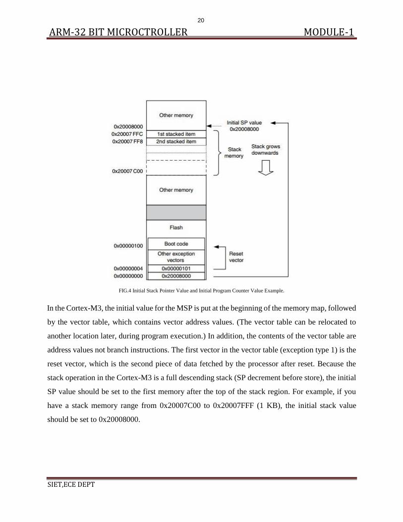
FIG.4 Initial Stack Pointer Value and Initial Program Counter Value Example.
In the Cortex-M3, the initial value for the MSP is put at the beginning of the memory map, followed
by the vector table, which contains vector address values. (The vector table can be relocated to
another location later, during program execution.) In addition, the contents of the vector table are
address values not branch instructions. The first vector in the vector table (exception type 1) is the
reset vector, which is the second piece of data fetched by the processor after reset. Because the
stack operation in the Cortex-M3 is a full descending stack (SP decrement before store), the initial
SP value should be set to the first memory after the top of the stack region. For example, if you
have a stack memory range from 0x20007C00 to 0x20007FFF (1 KB), the initial stack value
should be set to 0x20008000.
20