Embed Size (px)
Citation preview

1
COURSE MISSION
examine optical and electronic processes in organic molecules and polymers
that govern the behavior of practical organic optoelectronic devices
Vladimir Bulović
Welcome to 6.973Welcome to 6.973~ Organic ~ Organic OptoOpto--Electronics ~Electronics ~
@ MITFebruary 4, 2003 - Lecture 1
2
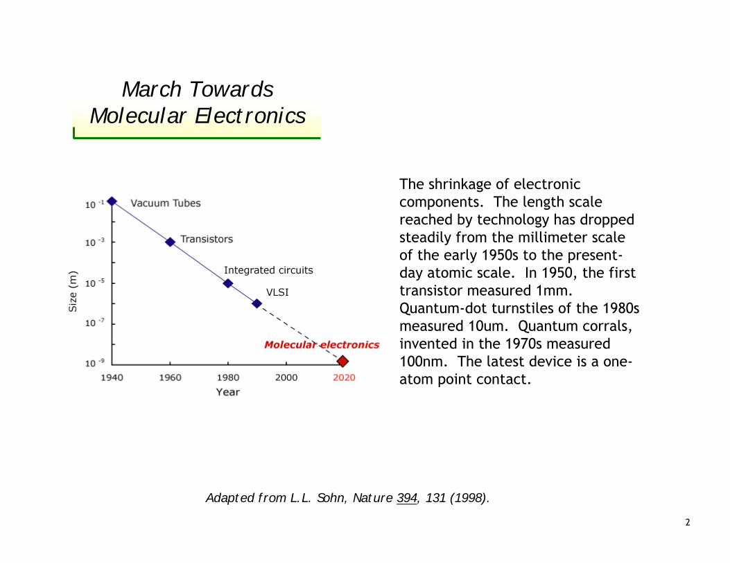
March Towards Molecular Electronics
Adapted from L.L. Sohn, Nature 394, 131 (1998).
The shrinkage of electronic components. The length scale reached by technology has dropped steadily from the millimeter scale of the early 1950s to the present-day atomic scale. In 1950, the first transistor measured 1mm. Quantum-dot turnstiles of the 1980s measured 10um. Quantum corrals, invented in the 1970s measured 100nm. The latest device is a one-atom point contact.
3
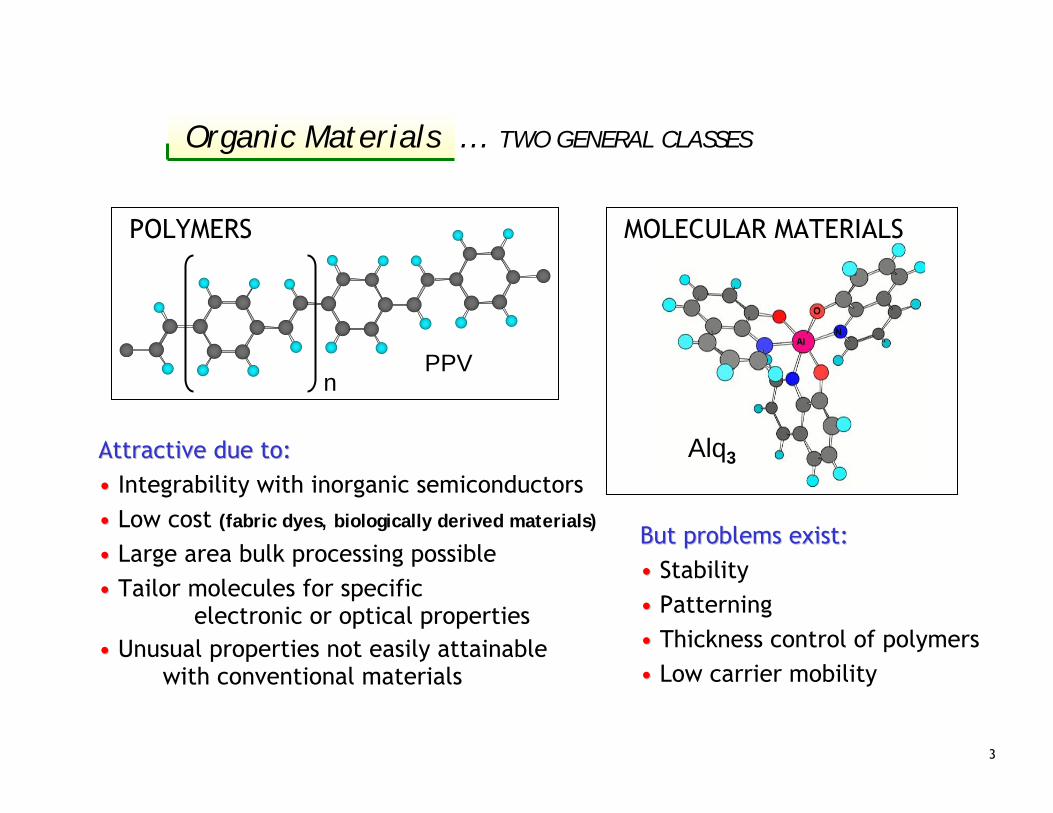
Organic Materials … TWO GENERAL CLASSES
Alq3
MOLECULAR MATERIALS
Attractive due to:Attractive due to:•• Integrability with inorganic semiconductors•• Low cost (fabric dyes, biologically derived materials)
•• Large area bulk processing possible•• Tailor molecules for specific
electronic or optical properties•• Unusual properties not easily attainable
with conventional materials
PPV
POLYMERS
n
But problems exist:But problems exist:•• Stability•• Patterning•• Thickness control of polymers•• Low carrier mobility

4
Scientific Interest in Organic Materials
• 1828 - Wöhler first synthesized ureawithout the assistance of a living organism
• 1950’s - steady work on crystalline organics starts
• 1970’s - organic photoconductors (xerography)
• 1980’s - organic non-linear optical materials
• 1987 - Kodak group published the first efficient organic light emitting device (OLED)
• Since then, the field has dramatically expandedboth commercially and scientifically(OLEDs, transistors, solar cells, lasers, modulators, ... )
to date, about two million organic compounds have been madeto date, about two million organic compounds have been made-- this constitutes nearly 90% of all known materials this constitutes nearly 90% of all known materials --

5
The Royal Swedish Academy of Sciences awards the Nobel Prize in Chemistry for 2000 jointly to:
•Alan J. Heeger, University of California at Santa Barbara, USA,
•Alan G. MacDiarmid, University of Pennsylvania, Philadelphia, USA,
•Hideki Shirakawa, University of Tsukuba, Japan
"for the discovery and development of conductive polymers"Plastic that conducts electricity
We have been taught that plastics, unlike metals, do not conduct electricity. In fact plastic is used as insulation round the copper wires in ordinary electric cables. Yet this year's Nobel Laureates in Chemistry are being rewarded for their revolutionary discovery that plastic can, after certain modifications, be made electrically conductive. Plastics are polymers, molecules that repeat their structure regularly in long chains. For a polymer to be able to conduct electric current it must consist alternately of single and double bonds between the carbon atoms. It must also be "doped", which means that electrons are removed (through oxidation) or introduced (through reduction). These "holes" or extra electrons can move along the molecule - it becomes electrically conductive. Heeger, MacDiarmid and Shirakawa made their seminal findings at the end of the 1970s and have subsequently developed conductive polymers into a research field of great importance for chemists as well as physicists. The area has also yielded important practical applications. Conductive plastics are used in, or being developed industrially for, e.g. anti-static substances for photographic film, shields for computer screen against electromagnetic radiation and for "smart" windows (that can exclude sunlight). In addition, semi-conductive polymers have recently been developed in light-emitting diodes, solar cells and as displays in mobile telephones and mini-format television screens. Research on conductive polymers is also closely related to the rapid development in molecular electronics. In the future we will be able to produce transistors and other electronic components consisting of individual molecules -which will dramatically increase the speed and reduce the size of our computers. A computer corresponding to what we now carry around in our bags would suddenly fit inside a watch.
http://www.nobel.se/chemistry/laureates/2000/press.html
Nobel Prize in Chemistry for 2000

6
Electronic Processes inMolecules / Aggregates / Thin Films
T1S1
S0
FLU
OR
ESC
ENC
E
PHO
SPH
OR
ESC
ENC
E
ENERGY TRANSFER
FÖRSTER, DEXTERor RADIATIVE
INTE
RN
ALC
ON
VER
SIO
N
AB
SOR
PTIO
N
10 ps
1-10 ns
>100 ns
S1 a
nd T
1 st
ate
dens
ity
Ener
gy
Bulovic et al., Chem. Phys. Lett. 287, 455 (1998); 308, 317 (1999).´
AlqAlq33
DCM2 in AlqDCM2 in Alq33
low DCM2low DCM2 high DCM2high DCM2
Inte
nsity
[a.u
.]
Wavelength [nm]
Tim
e [n
s]
0.25 ns
0.50 ns
0.75 ns
1.00 ns 1.50 ns
2.00 ns
5.00 ns4
8
12
16
0
1
2
3
4
5
0
600 650 700 750
35 nm35 nmwavelength shift
10% DCM2 in Alq310% DCM2 in Alq3
Temporal ResponseTemporal Response
Solid State SolvationSolid State Solvation

7
STM scan ofordered PTCDA monolayer on HOPG
Organic Thin Films … may be AMORPHOUS or CRYSTALLINE
molecular orbital calculation of the electron density in the highest occupied molecular orbital of a PTCDA molecule
Agreement between the calculation and the experiment exemplifies maturity of
detailed understanding of electronic arrangement on molecules.
However, …DYNAMIC ELECTRONIC PROCESSES in
MOLECULES and MOLECULAR ASSEMBLIESare NOT WELL UNDERSTOOD
and present a topic of our research
8
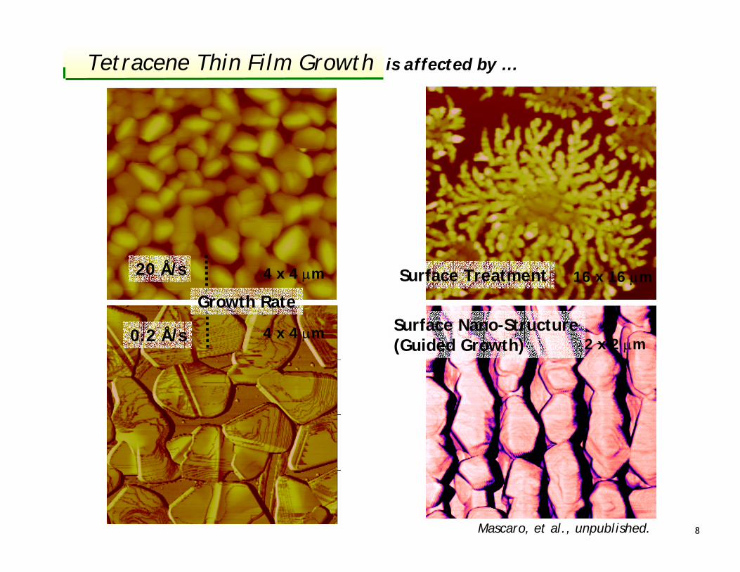
Tetracene Thin Film Growth is affected by …
Growth Rate
20 Å/s
0.2 Å/s
Surface Treatment
Surface Nano-Structure(Guided Growth)
4 x 4 µm
4 x 4 µm
16 x 16 µm
2 x 2 µm
Mascaro, et al., unpublished.

9
-VG
source drain
substrate
insulator gate
-VD
semiconductor
pentacene
Tdeposition=27 °CDR=1.0 Å/sec
µ~0.6 cm2 V-1 s-1
Adapted from Dimitrakopoulos, et. al., IBM J. Res. and Devel. 45, 11 (2001).
IMPROVED MOLECULAR ORDERING
Larger grain sizesLower defect densities
Enhanced mobility
Charge carrier mobility is
dependent on molecular order
within the semiconducting
thin film
Organic Field Effect Transistors
IBM
Plastic Logic
10
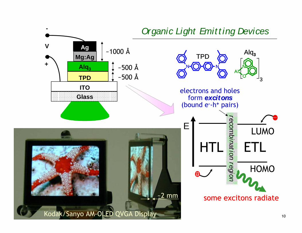
+
electrons and holesform excitonsexcitons
(bound e--h+ pairs)
some excitons radiatesome excitons radiate
HOMO
LUMO
recombination region
ETLHTL
E_
Kodak/Sanyo AM-OLED QVGA Display
~2 mm
Organic Light Emitting Devices
V
+
-
GlassITO
Alq3
TPD
Mg:AgAg
~1000 Å
~500 Å~500 Å
Alq3
AlN
O3
Alq3
AlN
O3
TPDN N
TPDN N

11
Opportunities …
• LEDs
• Lasers (Optically and Electrically Pumped)
• Solar Cells and Photodetectors
• Transistors
• Chemical Sensors
• Memory Cells
• Nano-Patterned Structures
• Materials Growth Technology
@ MIT
12
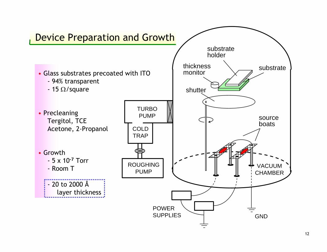
VACUUMCHAMBER
TURBOPUMP
COLDTRAP
ROUGHINGPUMP
substrateholder
thicknessmonitor
shutter
GND
substrate
POWERSUPPLIES
sourceboats
Device Preparation and Growth
• Glass substrates precoated with ITO- 94% transparent- 15 Ω/square
• PrecleaningTergitol, TCEAcetone, 2-Propanol
• Growth- 5 x 10⁻⁷ Torr- Room T
- 20 to 2000 Ålayer thickness

13
Wet N2 Glove Box
Load Lock
Ante Chamberand Oven
UV-OzoneLaminar Flow Hood
Dry N2 Glove BoxSample-Mask Storage
Probe Stationwith Cryostat
Integrated Materials Growth System
@ MIT
MIT lab of ORGANICOPTICS & ELECTRONICS
Physical & Vapor Phase Dep.
• molecular organics• nano-dots **• solvated polymers **• colloids **
Sputtering
• ITO• ceramics
Chemical Vapor Dep.chemically selective materials deposition
Evaporative Deposition
• molecular organics(amorphous and crystalline)
• metals
capable of in-situ growth and testingof multilayer structures and devices
SourceStorage
Sponsored by AFOSR and NSF

14
Wet N2 Glove Box
Load Lock
Ante Chamberand Oven
UV-OzoneLaminar Flow Hood
Dry N2 Glove BoxSample-Mask Storage
Probe Stationwith Cryostat
Integrated Materials Growth System
@ MIT
MIT lab of ORGANICOPTICS & ELECTRONICS
Physical & Vapor Phase Dep.
• molecular organics• nano-dots **• solvated polymers **• colloids **
Sputtering
• ITO• ceramics
Chemical Vapor Dep.chemically selective materials deposition
Evaporative Deposition
• molecular organics(amorphous and crystalline)
• metals
SourceStorage
SPINNERSPINNER
ANTE CHAMBERANTE CHAMBERand OVENand OVEN
ELECTRICAL and OPTICALELECTRICAL and OPTICALFEEDTHROUGHSFEEDTHROUGHS
Double Glove Box
Moisture Level < 1 ppm

15
Integrated Materials Growth System
Wet N2 Glove Box
Load Lock
Ante Chamberand Oven
UV-OzoneLaminar Flow Hood
Dry N2 Glove BoxSample-Mask Storage
Probe Stationwith Cryostat
@ MIT
MIT lab of ORGANICOPTICS & ELECTRONICS
Physical & Vapor Phase Dep.
• molecular organics• nano-dots **• solvated polymers **• colloids **
Sputtering
• ITO• ceramics
Chemical Vapor Dep.chemically selective materials deposition
Evaporative Deposition
• molecular organics(amorphous and crystalline)
• metals
SourceStorage SHADOW MASK
STORAGE-EXCANGE
SIX THERMALLY HEATED SOURCESTWO INDEPENDENT BANKS of THREE SOURCES EACH
E-BEAM EVAPORATIONSINGLE POCKET
INDEPENDENT SOURCE MONITORING
DURING CO-DEPOSITION
BASE PRESSURE ~ 7 X 10⁻⁸ torrThermal Evaporator
16
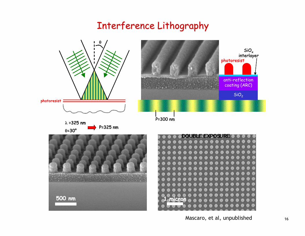
photoresist
λ =325 nm
θ=30°P=325 nm
θ
photoresist
λ =325 nm
θ=30°P=325 nm
λ =325 nm
θ=30°P=325 nm
θθ
500 nm
anti-reflection coating (ARC)
photoresist
SiO2
SiOxinterlayer
P=300 nm
500 nm500 nm
anti-reflection coating (ARC)
photoresist
SiO2
SiOxinterlayer
P=300 nm
500 nm500 nm 1 micron1 micron
Interference LithographyInterference Lithography
DOUBLE EXPOSURE
Mascaro, et al, unpublished

17
PDMSPDMS
500 nm500 nm500 nm 2 microns2 microns2 microns
Si or SiO2
photoresist
ARC
SiOx
Si or SiO2
PDMS
Si or SiO2
PDMS
Si or SiO2
PDMS
3. Remove PDMS “stamp”from the “master”
1. Interference lithography 2. Pour PDMS and cure 4. Evaporate organicmaterial on PDMS
3. Remove PDMS “stamp”from the “master”
1. Interference lithography 2. Pour PDMS and cure 4. Evaporate organicmaterial on PDMS
PDMS
Alq3 or TPD
PDMS
Alq3 or TPD
(a) (b) (c)
Sequence of steps for generating a PDMS PBG Sequence of steps for generating a PDMS PBG structure with an organic luminescent layer on topstructure with an organic luminescent layer on top
Lowell, Mascaro, et al

18
0
1
-1
[nm]
0 1 4 [µm]2 3
Reduce the size of active structures
… by stamping nano-featuresof monolayer thickness
5 µm 1 µm
Z scale = 3 nm
Mascaro, et al., unpublished.

19
Molecules Get WiredGood connections. Molecules can now be crafted into working circuits. Constructing real molecular chips will be a big challenge.
Memory Cells and FETsMolecular Switch
Hewlett-Packard
C. Collier, et al. Science 285, 391 (1999)

20
Image of Photosynthetic Machinery of Purple Bacteria
Solar CellsSolar Cellsand Photodetectorsand Photodetectors
21
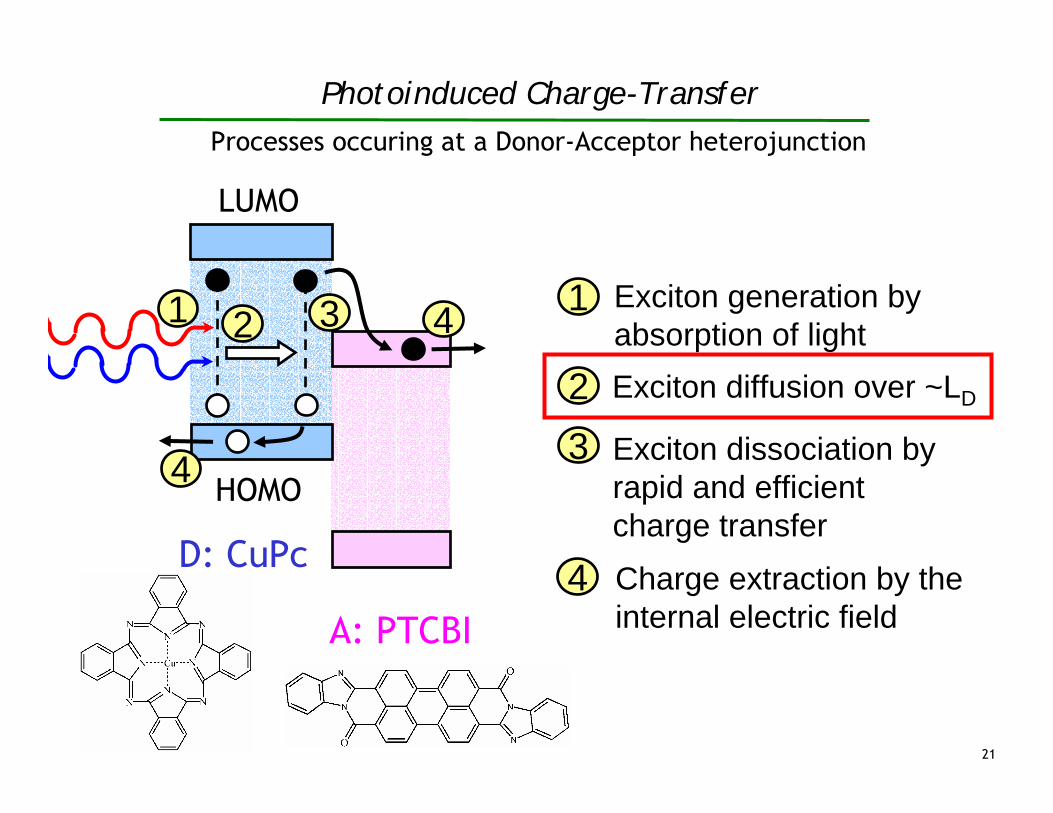
LUMO
HOMO
D: CuPc
A: PTCBI
2 3 4
4
Photoinduced Charge-Transfer
1
23
1 Exciton generation by absorption of light
4
Exciton diffusion over ~LD
Exciton dissociation by rapid and efficient charge transfer
Charge extraction by the internal electric field
Processes occuring at a Donor-Acceptor heterojunction
1 2 3 4
4
22
ISC
VOC
960
620
20064
192
-0.4 -0.2 0.0 0.2-80.0
-60.0
-40.0
-20.0
0.0
20.0
Voltage [V]
Cur
rent
[mA
/cm
2 ]
1300 mW/cm2
= 17 suns (AM1.5)
VMAX
IMAX
Organic Solar CellsI-V Response Under Solar Illumination
0.7
0.9
0.85 eV
CuPc(EG=1.7) PTCBI
(EG=1.7)
BCP(EG=3.5)
ITO
Ag
HOMO
LUMO
Energy Band Diagram
broadspectral response
300 – 800 nm
ηP ~ 3%in concentrator
geometry
Peumans, Bulovic, Forrest, Appl. Phys. Lett. (2000) Vol 76. p2650.

23
0
5
10
15
20
Laboratory
Production
Crystal
line-
Si
Poly-
Si
Amor
phou
s-Si
Orga
nic
[ % ]
Solar Cell Power Efficiency

24
Donor-Acceptor Multilayer Organic PhotodetectorsAdapted from Peumans, Bulovic, Forrest, Applied Physics Letters (2000). Vol 76. p3855
´

25
hν
electron
hole
CGL
CTL – hole transporter
anode cathode
1. A photon is absorbed into the CGL where it generates an exciton.
2. The exciton migrates to the interface between the two layers.
3. The charges separate and the hole moves into the CTL.
Xerography

26

27
120 million Rods – brightness6 million Cones – color
B 5-10%G ~30%R ~60%
Diagram of the Human Eye
From the NASA website

28
Luminescence and Lasing

29
CornflowerCornflower(alkaline sap)(alkaline sap)
PoppyPoppy(acidic sap)(acidic sap)
pelargonodin(anthocyanidins group)
30
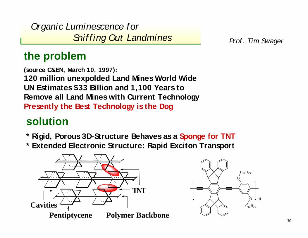
Organic Luminescence forSniffing Out Landmines
the problem(source C&EN, March 10, 1997):120 million unexpolded Land Mines World WideUN Estimates $33 Billion and 1,100 Years toRemove all Land Mines with Current TechnologyPresently the Best Technology is the Dog
solution* Rigid, Porous 3D-Structure Behaves as a Sponge for TNT* Extended Electronic Structure: Rapid Exciton Transport
TNT
Polymer BackbonePentiptyceneCavities
O
C14H29
O
C14H29
n
Prof. Tim Swager

31
FIDO 4D Field Test
≈10-16 g Detection Limit(100,000 Molecules)
Determining the TNT Concentration Profile of a AP-Landmine

32
400 500 600 700Wavelength [nm]
DCM
2 :
Alq
3
Rhod
. :
Alq
3
DCM
: A
lq3
C47
: CB
P
Pery
lene
: CB
P
PM :
Alq
3
PumpLaser
Edge Emission
InP SiO2 Alq:DCM
Kozlov, et al., Nature 389, 362 (1997).
Bulovic, et al., Science 279, 553 (1998). ´0 40 80 120 160
640
650
660
670
Lase
r Wav
elen
gth
(nm
)
Temperature (ºC)
INORGANIC
Temp. InsensitivityT0 = 1000
ORGANIC
Vertical Structures
Lateral Structuresδλ = (0.2 ± 0.1)
Å
6175 6180 6185Wavelength (Å)
HTL
Electrode
Alq3:DCM
DBR
Quartz
VCSELoutput
Alq3
(5 ± 1)°
ITO
Organic Semiconducting Lasers
33
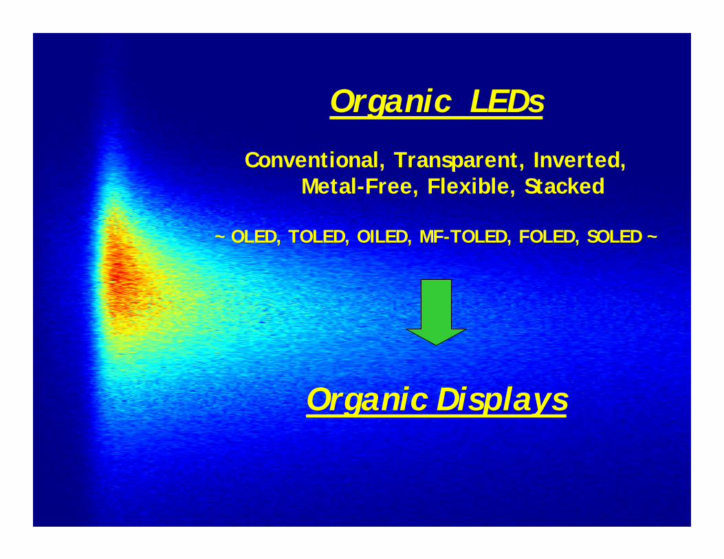
Organic LEDs
Conventional, Transparent, Inverted, Metal-Free, Flexible, Stacked
~ OLED, TOLED, OILED, MF-TOLED, FOLED, SOLED ~
Organic Displays

34
0
10
20
30
40
50
60
70
(BIL
LIO
NS
OF
DO
LL
AR
S)
1999 2000 2001 2002 2003 2004 2005Source: Display Search
20 to 30% growth per year$70 Billion business in 2005
Flat Panel Display Market

35
MultiMulti--FunctionFunctionVideo WatchVideo Watch
Rugged, high resolution, full-color, video-rate
displays enable a multitude of applications
AutomotiveAutomotiveDashboard displays,
external indicator lights, and road signs

36
Active WallpaperActive WallpaperLarge area displays
Active ClothingActive ClothingLight, rugged, low voltage,
flexible displays

37
Electroluminescence in Doped Organic Films
2.Excitons transfer to
luminescent dye
1.Excitons formed
from combinationof electrons and
holes
6.0 eV
a-NPD
2.6 eV
5.7eV
Alq3
2.7 eV electrons
exciton
trap states
low work functioncathode
transparent anode holes
dopant molecule(luminescent dye)
host molecules(charge transport
material)

38
400 500 600 700 800
0.0
0.2
0.4
0.6
0.8
1.0
Nor
mal
ized
EL
Inte
nsity
Wavelength [nm]
Alq3
PtOEP:Alq3
DCM2:Alq3
PtN N
NN
AlN
O 3
O
CNNC
N
α-NPDN N
Effect of Dopants on the OLED EL Spectrum

39
Cell Phone Display (Motorola/Pioneer)
LCD OLED

40
Kodak/Sanyo 5.5” AM-OLED Display, 2000
QVGA 5.5” QVGA 2.4”

41
Transparent OLEDs
> 70% transparent
• Future vision-area applications• Top emission for active matrix displays
-V+
EL Light
500 Å500 Å ITO
ETLHTLITO
Glass
EL Light
5050--100 Å100 Å Mg-Ag
Parthasarathy et al., Appl. Phys. Lett. 72, 2138 (1998).Bulovic et al., Nature 380, 29 (1996).´

42
OLEDs as Backlightsin AMLCDs
OLED backlight
AMLCD
anode cathode
computerinterface
TOLED Stack
R - offG - onB - off
R G Bsub-cycles
G sub-cycle
time
ONOFF
Timing Diagram
AMLCD
B-TOLED
G-TOLED
R-TOLED
reflector
AMLCD
TOLED Stack
R - offG - onB - off
R G Bsub-cycles
G sub-cycle
time
ONOFF
Timing Diagram
AMLCD
B-TOLED
G-TOLED
R-TOLED
reflector
AMLCD
Bulovic, patent pending.

43
Flexible OLED (FOLED)- Ultra lightweight- Thin form factor- Rugged- Impact resistant- Conformable
Manufacturing Paradigm ShiftWeb-Based Processing

44
FOLED-based Pixelated, Monochrome Display
Source: UDC, Inc.
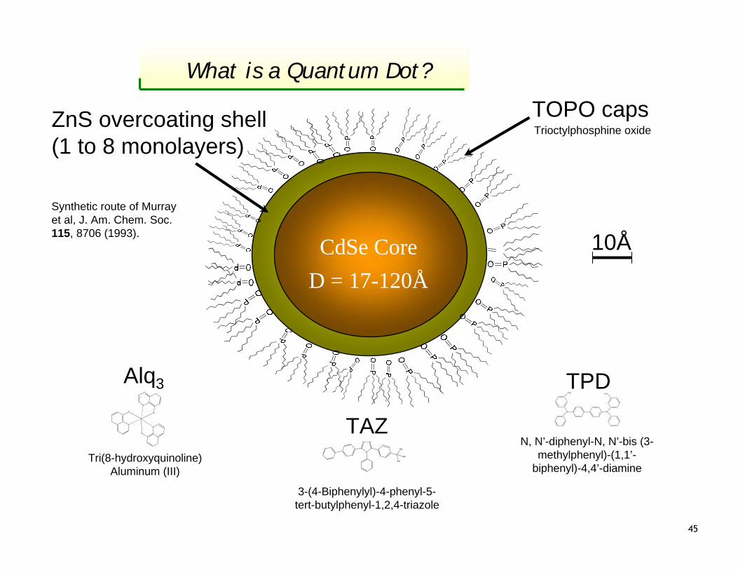
45
CdSe Core
ZnS overcoating shell (1 to 8 monolayers)
TOPO caps
What is a Quantum Dot?
D = 17-120Å
TAZ
3-(4-Biphenylyl)-4-phenyl-5-tert-butylphenyl-1,2,4-triazole
N
NN
Me
Me
Me
TPD
N, N’-diphenyl-N, N’-bis (3-methylphenyl)-(1,1’-
biphenyl)-4,4’-diamine
N
CH3
N
H3C
Alq3
Tri(8-hydroxyquinoline)Aluminum (III)
N
O
Al
N
O
N
O
10Å
Trioctylphosphine oxide
Synthetic route of Murray et al, J. Am. Chem. Soc. 115, 8706 (1993).
46
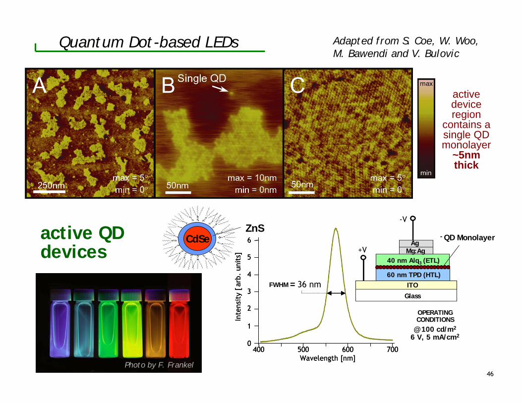
active QD devices
FWHM = 36 nm
CdSeZnS
CdSeZnS
400 500 600 700Wavelength [nm]
400 500 600 700Wavelength [nm]
0
1
2
3
4
5
6In
tens
ity
[arb
. un
its]
0
1
2
3
4
5
6In
tens
ity
[arb
. un
its]
OPERATINGCONDITIONS
@ 100 cd/m2
6 V, 5 mA/cm2
-V
60 nm TPD (HTL)
Mg:Ag+V
Glass
40 nm Alq3 (ETL)
- QD M
ITO
Ag
(a)
QD MonolayerCdSeZnS
Photo by F. Frankel
Quantum Dot-based LEDs Adapted from S. Coe, W. Woo, M. Bawendi and V. Bulovic
active device region
contains a single QD monolayer
~5nm thick
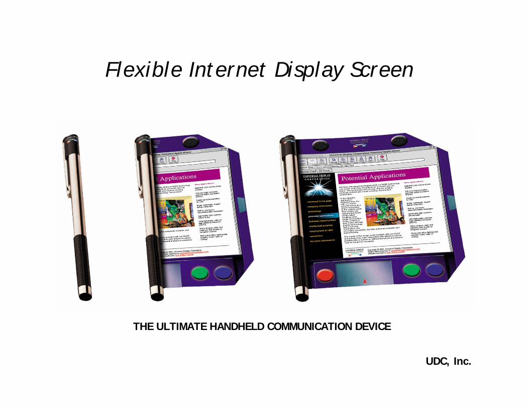
Flexible Internet Display Screen
THE ULTIMATE HANDHELD COMMUNICATION DEVICE
UDC, Inc.