Embed Size (px)
Citation preview

8/6/2019 Wei_links_chapter02 Energy-Efficient Design of High-Speed Links
http://slidepdf.com/reader/full/weilinkschapter02-energy-efficient-design-of-high-speed-links 1/39
1
Chapter #
Energy-Efficient Design of High-Speed Links
Gu-Yeon Wei1
, Mark Horowitz2, Jaeka Kim
2
1 Harvard University, 2Stanford University
1. INTRODUCTION
Aggressive CMOS technology scaling has enabled explosive growth in
the integrated circuits (IC) industry with cheaper and higher performance
chips. However, these advancements have led to chips being limited by the
chip-to-chip data communication bandwidth. This limitation has motivated
research in the area of high-speed links that interconnect chips [2]
[14][40][42][48] and has enabled a significant increase in achievable inter-
chip communication bandwidths. Enabling higher I/O speed and more I/O
channels improves bandwidth, but they can also increase power consumption
that eats into the overall power budget of the chip. Furthermore, complexity
and area become major design constraints when trying to potentially
integrate hundreds of links on a single chip. Therefore, there is a need for
building energy-efficient high-speed links with low design complexity.Power in synchronous CMOS digital systems is dominated by dynamic
power dissipation, which is governed by the following well-known equation:
CLK SWINGSW DYNAMIC F V Vdd C P ⋅⋅⋅⋅=α , (1)
where α is the switching activity, C SW is the total switched capacitance, V DD
is the supply voltage, V SWING is the internal swing magnitude of signals
(usually equals Vdd for most CMOS gates), and F CLK is the frequency of
operation. And since power is the rate of change of energy,
SWINGSW DYNAMIC
V Vdd C E ⋅⋅⋅=α . (2)

8/6/2019 Wei_links_chapter02 Energy-Efficient Design of High-Speed Links
http://slidepdf.com/reader/full/weilinkschapter02-energy-efficient-design-of-high-speed-links 2/39
2 Chapter #
Power consumption in analog circuits is simply set by the static current
consumed such that STATIC STATIC I Vdd P ⋅= . Technology scaling enables
lower power and energy in digital systems since the next generation process
scales both capacitance and voltage. Transistors also get faster, so it is
possible to run a scaled chip at higher frequencies, while still dissipating less
power.
Aside from technology scaling, reducing just the supply voltage for agiven technology enables significant reduction in digital power and energy
consumption since both are proportional to the supply voltage squared.
However, voltage reduction comes at the expense of slower gate speeds. So,
there is a trade off between performance and energy consumption.
Recognizing this relationship between supply voltage and circuit
performance, dynamically adjusting the supply voltage to the minimum
needed to operate at a desired operating frequency enables one to reduce the
energy consumption down to the minimum required. This technique is
referred to as adaptive power-supply regulation, and requires a mechanism
that tracks the worst case delay path through the digital circuitry with respect
to process, temperature, and voltage in order to determine the minimum
supply voltage required for proper operation. Although it was first applied todigital systems, adaptive supply regulation can also enable energy-efficient
high-speed link design. It is one of several energy reduction techniques we
will investigate in this chapter.
The design of energy-efficient links relies on optimizing all components
of the interface. This optimization requires an analysis of each component
comprising the link and making the right power/performance trade offs. In
order to understand these trade offs, Section 2 presents an overview of link
design. Then, Section 3 investigates several approaches used in digital
systems that can also be applied to build energy-efficient links. It begins
with concepts utilizing parallelism to reduce power consumption.
Subsequently, an adaptive supply regulation technique is introduced that
offers a scheme for optimizing energy consumption in the overall link architecture. Section 4 presents implementation details of various test chips
that employ many of the techniques described in Sections 2 and 3 to build
energy-efficient serial links and link building blocks.

8/6/2019 Wei_links_chapter02 Energy-Efficient Design of High-Speed Links
http://slidepdf.com/reader/full/weilinkschapter02-energy-efficient-design-of-high-speed-links 3/39
#. Energy-Efficient Design of High-Speed Links 3
2. OVERVIEW OF LINK DESIGN
RX
d a t a i n
timingrecovery
10010
channel
TX
d a t a o u t
10010
Figure 1. Link components
High-speed links can provide high communication bandwidths between
chips and consist of four major components as shown in Figure 1. A
serializer converts parallel data bits into a high-speed serial bit stream that
sequentially feeds a transmitter. The transmitter then converts the digital
binary data into low-swing electrical signals that travel through the channel.
This channel is normally modeled as a transmission line and can consist of
traces on a printed circuit board (PCB), coaxial cables, shielded or un-
shielded twisted pairs of wires, traces within chip packages, and theconnectors that join these various parts together. A receiver then converts the
incoming electrical signal back into digital data and relies on a timing
recovery block to compensate for delay through the channel and accurately
receive the data. A de-serializer block converts the received serial bit stream
into parallel data and re-times the data to the clock domain of the rest of the
digital system that consumes it.
clk
I/O clk
data
Vref
DLL
TX RX
Figure 2. Source-synchronous parallel link interface
Links commonly used in modern digital and communication systems can
be categorized into two forms – parallel and serial links. High-speed serial
links are better suited for applications that are pin and channel limited such
as the backplane communication in router and switch boxes [15][20][45].
They are also used as components in multi-gigabit optical links [19][37].

8/6/2019 Wei_links_chapter02 Energy-Efficient Design of High-Speed Links
http://slidepdf.com/reader/full/weilinkschapter02-energy-efficient-design-of-high-speed-links 4/39
4 Chapter #
Serial links tend to be over long distances and therefore emphasize
maximizing bits per second through a single channel with considerable effort
required to overcome non-ideal channel characteristics. Other systems that
require high-bandwidth communication between chips, with less stringent
restrictions on pin and channel resources, can utilize several parallel sets of
these data links. One implementation example of this type of interface is
called a source-synchronous parallel interface [42] presented in Figure 2. Itrelies on a separate clock signal for accurate timing recovery, which is
shared by the parallel links, and requires delays through each channel match
one another. This can be achieved through careful matching of the channel
lengths and augmented with delay compensation schemes to account for
residual mismatches [56]. Since the basic components comprising both
parallel and serial links are the same, as the chapter delves into design details
and issues, no distinction will be made as to whether they are for serial or
parallel links unless discussed explicitly.
In order to understand link operation and investigate ways to reduce
energy consumption, this section begins with a review of the different
figures of merit that govern high-speed link performance. Then, we
investigate how different design choices affect power and performance ineach of the components described in the following subsections. It is
important to note the design choices to be made are governed by the specific
environment, technology, and system-level requirements of each design.
Therefore, trade offs are presented so that the designer can make the
appropriate compromises to converge on an energy-efficient design.
2.1 Figures of Merit
The performance and reliability of high-speed links depends on several
figures of merit. Besides the raw number of bits transmitted per second, the
quality of the signal determines whether the receiver can accurately decipher
the waveform back into digital data. If the signal is indecipherable, then bit
rate is meaningless. Therefore, we need a way of looking at the received
signal and determine its quality. We can look at an eye-diagram using
voltage and timing margins as quantitative measures of link quality, which
can be used as metrics for comparing performance trade offs. Lastly, bit-
error rate is another figure of merit for a link’s ability to reliably transmit
and receive data.

8/6/2019 Wei_links_chapter02 Energy-Efficient Design of High-Speed Links
http://slidepdf.com/reader/full/weilinkschapter02-energy-efficient-design-of-high-speed-links 5/39
#. Energy-Efficient Design of High-Speed Links 5
random bit stream
ideal link real link
Tbit
Figure 3. Received eye diagrams
Figure 3 presents eye-diagrams for ideal and real links, where the x-axis
spans two bit times in order to show both leading and falling transitions of
the data signal. For a random data sequence, there are both falling and rising
transitions at each bit interval. While the data levels and bit intervals are
clearly defined for the ideal case, real systems suffer from process
variability, environmental changes, and various noise sources that interact
with the signal to blur (or close) the eye. Notice that the high and low
voltage levels are no longer well-defined levels, but occur over ranges. The
same holds true for the transition times. Qualitatively, larger eye openings
represent more reliable links. Quantitatively, we can apply two metrics to
measure its quality – voltage margin and timing margin. The vertical eye
opening, measured in the middle, determines how much voltage margin the
receiver has in determining whether the received signal is a high- or low-
level. The horizontal opening provides a measure of how well the receiver
can decipher one data bit from the next. Due to the finite slope of edge
transitions, reduction in voltage margin also leads to narrower timing
margins.
Besides environmental variation and noise in the transceiver circuits,there are non-idealities in the channel that degrade signal quality. Therefore,
an eye-diagram at the receiver presents a more realistic picture of link
performance than one measured at the transmitter. Unfortunately, even
measuring at the receiver doesn’t provide the whole picture. There can be
voltage and timing offsets in the receiver and the designer must subtract
these offsets from the measured margins. Furthermore, since the
measurement occurs over a finite time interval, it cannot fully capture the
effects of unbounded random noise sources (e.g. thermal noise, 1/f noise,
device noise, etc.) that are represented as probabilistic distributions with
infinite tails. So instead of relying only on margins, designers present link
reliability in terms of the bit-error rate (BER), which is the probability that
an error will occur with some frequency. This probability is an exponential
8/6/2019 Wei_links_chapter02 Energy-Efficient Design of High-Speed Links
http://slidepdf.com/reader/full/weilinkschapter02-energy-efficient-design-of-high-speed-links 6/39
6 Chapter #
function of the excess signal margins divided by the RMS distribution of the
random noise sources [39]. Increasing margins and reducing noise improve
BER, but may come at the expense of higher power consumption. Therefore,
understanding and making the right trade offs between performance and
power is important. Let us take a look at what some of these trade offs are by
reviewing the operation of the link components, beginning with the
transmitter.
2.2 Transmitter
The transmitter converts binary data into electrical signals that propagate
through an impedance-controlled channel (or transmission line) to a receiver
at the opposite end. This conversion must be done with accurate signal levels
and timing for a reliable high-speed communication link. Link designers
commonly use high-impedance current-mode drivers in single-ended or
differential configurations, and there are various choices for terminating the
signals through the impedance-controlled channel. This subsection
investigates these different transmitter options and looks at how they impact
power/energy consumption. Lastly, controlling the slew rate of thetransmitted signal is desirable for minimizing noise coupling into the
channel. Since lower noise solutions enable lower power, this section
presents several techniques for slew-rate controlled transmitters. We will
start the discussion with a single-ended high-impedance driver.
2.2.1 High-impedance Drivers
ZO
= 50Ω
Rx
50Ω
ZO
= 50Ω
Rx
50Ω
ZO
= 50Ω
Rx
50Ω
transmitter-only
termination
receiver-onlytermination
double termination
Figure 4. Ideal high-impedance drivers
A high-impedance driver utilizes a current source switch operating in
saturation to push signals through a channel as shown in Figure 4.

8/6/2019 Wei_links_chapter02 Energy-Efficient Design of High-Speed Links
http://slidepdf.com/reader/full/weilinkschapter02-energy-efficient-design-of-high-speed-links 7/39
#. Energy-Efficient Design of High-Speed Links 7
Characteristics of the signal transmission depend on the choice of
termination used. The simplest scenario is to use a matched-impedance
terminator at either the transmitter or receiver side of the link. With
transmitter-only termination, there is a voltage divider formed at the source
and a voltage waveform, with amplitude set by 2Ο⋅ R I DRIVE , propagates
down the channel. Assuming a perfect open-circuit termination at the
receiver, with reflection coefficient Γ =1, the waveform amplitude doubles atthe receiver. Then the signal reflects back to the source and its energy is
absorbed by the termination resistor at the transmitter, given that it’s
impedance matches that of the channel. Receiver-only termination behaves
similarly, except that a current is transmitted through the channel and the full
voltage amplitude, Ο⋅ R I DRIVE , is seen at the receiver. In either case, the
same voltage amplitude of the signal is seen at the receiver. However,
utilizing single termination on either the transmitter or receiver side has
some disadvantages stemming from non-idealities in implementation.
Achieving perfect matched-impedance termination can be difficult due to
tolerances in the channel and components. There may also be discontinuities
in the channel due to package parasitics and connectors. These non-idealities
lead to amplitude noise as energy sloshes back and forth through the channelarising from imperfect termination. Other discontinuities throughout the
channel exacerbate this situation. Consequently, designers use double
termination with matched-impedance termination resistors on both sides of
the link. In that case, the energy of the transmitted voltage waveform is
absorbed at the receiver with amplitude 2Ο⋅ R I DRIVE seen at the receiver.
Although the swing amplitude is now smaller, residual energy that sloshes
back and forth due to impedance mismatches attenuates twice as quickly
since the energy is absorbed on both sides. Hence, the signal to noise ratio
(SNR) can be smaller with double termination.
2.2.2 Single-ended vs. Differential
D D
DD
Figure 5. Differential signalling implementations

8/6/2019 Wei_links_chapter02 Energy-Efficient Design of High-Speed Links
http://slidepdf.com/reader/full/weilinkschapter02-energy-efficient-design-of-high-speed-links 8/39
8 Chapter #
So far, we have looked at a single high-impedance driver that transmits
an analog waveform through the channel. In order to convert this signal back
into data bits, we must know its voltage and timing characteristics. More
specifically, we need some voltage and timing references with respect to
which the signal can be deciphered as a logical “1” or “0” and distinguish
adjacent bits (timing issues will be discussed in Section 2.4). In single-ended
links, unless fixed transmitted voltage levels with a common reference suchas Vdd or Ground are known and shared by both sides of the link, an
additional voltage reference is required. This additional reference, set to half
the transmitted signal amplitude, can be transmitted along with the data and
the ability to vary the transmitted level enables lower power dissipation. In
the case of parallel links, several channels may share a single reference line
and overhead of the reference line can be amortized across them all. For
serial links, a reference voltage line may also be used, but designers will
more commonly use a differential signaling scheme, where a pair of wires
carries complementary signals. Two implementations are illustrated in
Figure 5. One uses a differential pair with a single current source that sets
the output swing. The other implements a pair of single-ended transmitters
each transmitting complementary data. The drawback of using a differentialpair arises from the reduced gate overdrive on the output devices. Using
larger devices can enable the same current drive at the expense of larger
capacitive loading on both the inputs and outputs that can limit bandwidth
and increase power.
A differential transmitter has several nice properties. The current
consumption of the link is constant and does not induce voltage spikes in the
power supply lines arising from parasitic inductance in the packaging. Tight
coupling of the lines enables low electro-magnetic interference (EMI) since
the return currents for the signals are through the adjacent wires. Lastly,
differential signals present larger effective signal amplitudes to the receiver
compared to a single-ended signal to facilitate the conversion of the signal
energy into digital data bits. However, these come at the cost of higher pinresources. Thus, differential signaling is common in serial link designs, but
parallel links often require single-ended interfaces to reduce pin count.
Although differential signaling may appear to require higher power
dissipation since there are now two channels that switch, this is not always
the case. There have been recent investigations that compare single-ended
and differential signaling that show lower signal-to-noise ratios are
achievable with differential signaling leading to lower transmitted swing
levels [52]. Line power is a function of the transmitted voltage swing as
shown by the following equation:

8/6/2019 Wei_links_chapter02 Energy-Efficient Design of High-Speed Links
http://slidepdf.com/reader/full/weilinkschapter02-energy-efficient-design-of-high-speed-links 9/39
#. Energy-Efficient Design of High-Speed Links 9
2 / Ο
⋅⋅= R
V Vdd P
swingα , (3)
where Vdd is the supply voltage, RΟ is the transmission line and termination
impedance, and α is the signal’s activity factor. Therefore, lower power links
are possible with differential signaling.
2.2.3 Slew-rate control
(a)
τ τ
(b)
Figure 6. Slew-rate control implementations
So far, we have seen that reducing noise can lead to lower power link
designs. Package and connector non-idealities can be another source of
noise. High-frequency energy in the transmitted signal can interact with
parasitic RLC tanks to cause ringing in the line and coupling (cross talk) into
adjacent lines. Therefore, high-speed link designs often limit the edge rate of
transmitted signals to mitigate these effects. Implementing edge-rate control
is fairly straightforward and several examples can be found in the literature.
There are two general approaches used to implement edge-rate control. The
technique illustrated in Figure 6-(a) limits the slew rate of signals by
controlling the RC time constant of the driver’s input signal [30]. This is can
be achieved by adjusting the capacitive loading or by changing the drive
strength of the preceding predriver buffer and thereby varying its effective
output resistance. In so doing, the edge-rate of the signal also slews
accordingly at a controlled rate. Another technique, presented in Figure 6-
(b), breaks the driver input into smaller parallel segments and slews the
output by driving the segments in succession with some delay τ (often
implemented with an RC delay line) [9]. Care must be taken to guarantee
that the time constants of the signal slew are fixed proportional to the symbol
rate. Since both the RC of the predriver and τ of delay elements are
dependent on process and operating environments, some mechanism for
controlling them are required. Time constants can be controlled manually or

8/6/2019 Wei_links_chapter02 Energy-Efficient Design of High-Speed Links
http://slidepdf.com/reader/full/weilinkschapter02-energy-efficient-design-of-high-speed-links 10/39
10 Chapter #
with a simple control loop that relies on a process and environment
monitoring circuit. An inverter-based ring oscillator is a good example of
such a circuit [30]. The oscillation period of the ring is directly related to
process and environmental conditions. Therefore, by counting the
oscillations over a known period, a digital control loop can converge to the
appropriate slew-rate settings for the symbol rate. A system level approach
to this basic concept that utilizes knowledge of the process andenvironmental conditions of a chip can be extended to other parts of the link
interface to enable energy-efficient designs [52][28] and are discussed in
more detail in Sections 3 and 4.
2.3 Receiver
At the opposite end of the channel, a receiver circuit deciphers the
incoming analog signals into digital data bits. This block commonly consists
of a differential sampling circuit that samples the data in the middle of the
received symbol and amplifies the low-swing signal to binary levels. Single-
ended signaling connects the signal line to one input of the differential pair
while the other is set to a reference voltage to which the signal is compared.Differential signaling connects each signal line to each side of the input
buffer. So, the effective voltage swing seen by the receiver is much greater
for differential signaling than single-ended signaling for the same swing
magnitudes. This effect enables differential signaling to require smaller
voltage swings, which can lead to lower power consumption.
D
S/H
D
(a) (b)
s a m p l e r
s a m p l e r
Figure 7. Integrating receiver (a) and tracking-bandwidth receiver (b) schematics
While direct sampling of the incoming signal enables a simple design,
link designs often add a preconditioning stage before the sampler [11].
Preconditioning has several advantages: it enables higher common-mode
rejection to relax the input dynamic range requirements of the sampler; it
isolates the sampler from injecting noise back into the channel; and it offers
a way to filter the incoming signal. There are a few ways in which to
implement this preconditioning. One commonly used technique converts the

8/6/2019 Wei_links_chapter02 Energy-Efficient Design of High-Speed Links
http://slidepdf.com/reader/full/weilinkschapter02-energy-efficient-design-of-high-speed-links 11/39
#. Energy-Efficient Design of High-Speed Links 11
voltage into a current and integrates charge over the bit time to convert the
current back into a voltage signal that can be sampled and is called a current-
integrating receiver [41]. The integration has several desirable properties
when receiving high-speed signals. Cross talk resulting from coupling can
corrupt signals. If a noise event occurs right at the sampling point of the
received signal, it can significantly degrade voltage margins and make the
signal indistinguishable. To avoid this problem, an integrating receiver doesnot only look at the data at one moment in time but over the entire bit time.
Figure 7-(a) illustrates its implementation. The input voltage waveform
steers current through the differential pair from the integrating capacitors
and a sample-and-hold circuit delivers the measured voltage difference to a
sampler that amplifies the signal to digital logic levels. Integration mitigates
the effects of high-frequency noise. An alternative way to think about this is
that the integration implements a filter with its bandwidth equivalent to the
symbol rate. Hence, coupling noise events, which are normally high
frequency disruptions, are filtered out. The noise rejection capabilities of the
integrating receiver effectively can lead to a more energy-efficient design
since larger swings are not necessary to overcome noise from cross talk.
Rather, the minimum signal swing magnitudes required for this type of receiver may depend on swing levels necessary to overcome offsets in the
differential pair and sampler. Minimizing offsets in the receiver via
calibration can lead to robust link designs with extremely low swing levels
[31].
A similar preconditioning scheme relies on an amplifier to buffer the
incoming signal from the sampler. In order to achieve similar noise rejection
characteristics of the integrating receiver, the amplifier ought to have a
limited bandwidth set to no greater than the symbol rate of the incoming
signal. The bandwidth of this amplifier must not only track the incoming
symbol rate, but do so in the presence of process and environmental
variations. Figure 7-(b) presents a schematic of this type of receiver where
the bandwidth of the front-end amplifier is set by its output RC time constant[52]. If the load’s impedance can track bit rate, process, and operating
conditions, the bandwidth can be set to reject high-frequency noise and only
allow energy up the symbol rate pass through, like the integrating receiver.
2.4 Clock Synthesis and Timing Recovery
Both the transmission and reception of data symbols in high-speed links
must operate in lock step with respect to an accurate timing reference.
Deviations from ideal timing reference points can lead to errors in
communication and therefore timing jitter and offsets must be limited.. As a
review, this section presents approaches commonly used to generate clock

8/6/2019 Wei_links_chapter02 Energy-Efficient Design of High-Speed Links
http://slidepdf.com/reader/full/weilinkschapter02-energy-efficient-design-of-high-speed-links 12/39
12 Chapter #
signals for the transmitter and receiver. Both blocks normally rely on a
phase- or delay-locked loop (PLL or DLL) to generate on-chip clock signals
that are locked with respect to an external reference. The selection of
utilizing either a PLL or DLL depends on the system-level environment due
to their respective advantages and disadvantages for generating low-jitter on-
chip clock signals. While the loops share several common building blocks,
their operation differs as a function of their configuration. A PLL mustintegrated frequency in order to achieve lock while a DLL simply adjusts
delay [16][26].
These differing configurations lead to different input-to-output phase
transfer functions for each loop. The closed-loop phase transfer function of a
PLL exhibits a low-pass filter characteristic. Hence, it has the property of
rejecting high frequency noise from the input while tracking noise within the
bandwidth of the loop. The VCO frequency is driven as a function of the
phase error, but there is no direct signal path between the input clock source
and the on-chip clock. However, in the case of a DLL, the on-chip clock is
directly connected through delay elements to the input clock source and the
input-to-output phase transfer function is effectively an all-pass filter. This
apparent drawback limits the appeal of using DLL’s in systems that sufferfrom a noisy input clock source. However, a DLL has advantages over a
PLL when internal noise sources (e.g. power supply noise) dominate. Since a
PLL relies on an oscillator, if a noise event perturbs an edge in the VCO, the
oscillator will recirculate the noise until the loop can compensate for it at a
rate set by the bandwidth of the loop. Therefore, wide bandwidth is desirable
to quickly recover from jitter due to on-chip noise [36]. On the other hand, a
DLL does not accumulate jitter over multiple clock cycles since the delay
line is reset every cycle. Hence, lower jitter may be possible with a DLL
when on-chip noise sources are the dominant cause of jitter.
Transmitters can utilize either a PLL or DLL to generate an on-chip clock
signal with respect to which data symbols are driven onto the channel [24].
High performance links often operate at bit rates higher than the block thatsupplies the data. Therefore, the clock generator also serves to align and
serialize the parallel data. This often requires clock frequency multiplication
to generate a higher clock rate for data transmission with respect to the lower
clock rate at which the parallel data feeds the transmitter. In order to
minimize timing uncertainty, the clock signal (or edge) ought to be
combined with the data at the latest possible point in the transmitter
datapath. However, drivers can be large in order to drive long distances and
present an appreciable capacitive load to the clock generator. Since the
activity factor of a clock signal is higher than the data, combining the data
with the clock signals before the ramp-up buffer chain can trade timing

8/6/2019 Wei_links_chapter02 Energy-Efficient Design of High-Speed Links
http://slidepdf.com/reader/full/weilinkschapter02-energy-efficient-design-of-high-speed-links 13/39
#. Energy-Efficient Design of High-Speed Links 13
uncertainty for energy efficiency. Other clocking strategies to enable energy
efficiency will be presented in Section 3.
The receiver also relies on a PLL or DLL to align the on-chip clock
signals with respect to the incoming data symbols in order to accurately
sample the data and differentiate successive bits from one another. The
specific implementation of the timing recovery circuit depends on the
architecture of the link. For source-synchronous parallel links, where a clock signal is transmitted in parallel with the data, the clock-recovery loop locks
to the received clock signal and is used to sample the data signals. When no
explicit clock signal is provided, the timing-recovery block must extract
timing information directly from the data stream utilizing a phase detecting
block.
mux
Core Loop
0o 360o
ΦREF
PDDIN
or ΦIN
Digital Control
Interpolator
Figure 8. Dual-loop DLL block diagram
In either configuration, a robust example of clock recovery utilizes a
dual-loop architecture introduced by Sidiropoulos, et al in [44] and
illustrated in Figure 8. It relies on a core loop that generates coarsely spaced
clock edges that evenly span a clock period. These clock edges can be
generated with either a PLL or DLL. Then, a secondary loop utilizes an
interpolator to generate a finely spaced clock edge aligned to the incomingdata symbols. A phase detecting block drives control circuitry that generates
a control word to select an adjacent pair of clock edges from the core loop
and appropriately weight the contribution of each edge in order to slide the
resulting on-chip clock edge into lock. This dual-loop scheme not only offers
infinite capture range which is a limitation for conventional DLL’s, but with
a sufficiently high slewing capability it can accommodate small frequency
differences between the core loop’s clock rate (ΦREF) and the data rate of the
received signal. This ability to compensate for frequency differences is
important for high-speed links because the opposite ends of a transceiver
may not share a common clock source.
Although the clock generation for the transmitter and receiver were
introduced separately, since the transmitter and receiver for different

8/6/2019 Wei_links_chapter02 Energy-Efficient Design of High-Speed Links
http://slidepdf.com/reader/full/weilinkschapter02-energy-efficient-design-of-high-speed-links 14/39
14 Chapter #
channels reside on the same die, they may share some of the clock
generating components. More specifically, the core loop described for timing
recovery of a receiver may also serve as the clock generator for an adjacent
transmitter [6]. Such sharing of components not only reduces circuit
redundancy, but it obviates issues arising from having multiple loops on the
same substrate1. Moreover, on-chip clock generation and distribution is a
significant source of power consumption in high-speed links and efforts toreduce this power can enable a much more energy-efficient design.
2.5 Summary
This section has provided a brief overview of high-speed link design.
Several approaches for implementing each of the components are possible,
but the designer must first understand the system-level noise characteristics
in order to converge on the most efficient design. In both the transmitter and
receiver, a lower noise solution leads to lower energy since extra voltage
margins can be avoided. In clock generation and timing recovery, precise
placement of clock edges not only enables higher performance, but may also
enable some trade offs between timing margin and energy.As modern high-speed links strive for bit rates on the order of multiple
Giga-bits per second or higher, intrinsic losses in the channel due to
dielectric and skin loss can significantly degrade performance. The channel
looks like a low pass filter out at frequencies greater than 1-GHz for 50-Ω
traces on a printed circuit board [7]. This frequency-dependent attenuation
leads to inter-symbol interference, which can severely close the received
eye. This is not a new problem, but one copper-base wire-line
communication links (e.g. DSL, Ethernet) have been contending with. A
common solution is to use equalization schemes to compensate for the low-
pass characteristics of the channel. Several high-speed link designs also
employ a type of equalization at the transmitter called pre-emphasis
[8][12][13], where the transmitter pre-distorts the signal in anticipation of
the filtering caused by the channel. While equalization or pre-emphasis
enables links to achieve higher bandwidths, it can be fairly complex and
costly in terms of power.
In order to see what other techniques are available for reducing power
consumption in high links, the next section describes several approaches for
1When multiple PLL’s are integrated onto the same substrate, they may suffer from
injection locking if not isolated from one another and can be a significant source of clock
jitter [29].

8/6/2019 Wei_links_chapter02 Energy-Efficient Design of High-Speed Links
http://slidepdf.com/reader/full/weilinkschapter02-energy-efficient-design-of-high-speed-links 15/39
#. Energy-Efficient Design of High-Speed Links 15
enabling energy efficiency by exploiting parallelism and an adaptive supply-
regulation technique.
3. APPROACHES FOR ENERGY EFFICIENCY
Now that we have an understanding for how some of the different designchoices affect the energy efficiency of high-speed link designs, this section
further investigates approaches specifically targeted to improve energy
efficiency. Energy consumption has been a growing concern in building
large digital systems (e.g. microprocessors) and has led to several
advancements to reduce power consumption [5][10][23]. Since high-speed
links are by nature mixed-signals designs (consisting of both digital and
analog circuits), we can leverage many of the observations and techniques
applied to digital systems to build energy-efficient links. One approach can
be as simple as taking advantage of the next generation process technology
to enable lower energy consumption for the same performance. Parallelism
is another technique that digital designers have used to reduce power without
sacrificing performance. This section looks at several forms of parallelismthat are also possible in link design. Lastly, adaptive power-supply
regulation, a technique that has enabled energy-efficient digital systems, is
introduced and its application to the design of high-speed links is presented.
3.1 Parallelism
Parallelism has often been used in large digital systems as a way to
achieve higher performance while consuming less power, at the expense of
larger area. Breaking up a complex serial task into simpler parallel tasks
enables faster and/or lower power operation in the parallel tasks. For links,
the goal is to reduce power consumption in the overall design withoutsacrificing bit rate. An obvious way to parallelize an interface is to utilize
multiple links to achieve the desired aggregate data throughput (i.e. parallel
links). Parallel links can operate at lower bit rates in order to mitigate
channel non-idealities (e.g. skin and dielectric loss, and cross talk) and
enable an energy-efficient interface. However, this pin-level parallelism
comes at the expense of pin and channel resources, which are not always
abundant in many communication systems. Parallelism can also be applied
to individual links via two parameters – time and voltage. Examples of
parallelism in time is prevalent in modern link designs with double data-rate
(DDR) and quad data-rate (QDR) memory interfaces being the most visible
[57]. Parallelism in voltage can also be seen in many communication links
from several generations of Ethernet links to proprietary backplane

8/6/2019 Wei_links_chapter02 Energy-Efficient Design of High-Speed Links
http://slidepdf.com/reader/full/weilinkschapter02-energy-efficient-design-of-high-speed-links 16/39
16 Chapter #
transceiver designs . Both of these forms of parallelism offer higher
performance and/or power savings by reducing the internal clock rate within
the transceiver relative to the bit rate of the link. This section further
investigates both of these forms of parallelism in detail.
3.1.1 Sub-clock period symbols
0
0.1
0.2
0.3
0.4
0.5
0.6
0.7
0.8
0.9
1
5.6 5.8 6 6.2 6.4 6.6 6.8 7
N o r m a l i z e d S w i n g M a g n i t u d e
Clock Period (normalized to FO4 inverter delay)
0
0.1
0.2
0.3
0.4
0.5
0.6
0.7
0.8
0.9
1
5.6 5.8 6 6.2 6.4 6.6 6.8 7
N o r m a l i z e d S w i n g M a g n i t u d e
Clock Period (normalized to FO4 inverter delay)
Figure 9. Normalized clock swing vs. clock cycle time
The clock rate of a chip limits link performance when the bit rate is equal
to clock frequency. Even with aggressive pipelining to reduce the critical
path delay in the datapath, there is a minimum clock cycle time required to
distribute and drive the clock signal across the chip. As seen in Figure 9, as
the clock cycle time shrinks, expressed in terms of fanout-of-4 (FO4)
inverter delays2 on the x-axis, it experiences amplitude attenuation as it
propagates through a chain of inverters [54]. The minimum cycle time that
can be propagated is roughly 6 inverter delays. Transmitting at this clock
rate limits the bit rate to less than 1-Gb/s in a 0.25-µm technology. However,
higher bit rates are desirable in high-speed links and therefore transmittingseveral bits within a clock cycle are required for higher data rates.
Transmitting multiple bits within a clock period is not only a way to improve
performance, but it also offers a way to reduce power consumption in the
interface. Multiple clock phases can be generated using a ring oscillator or
delay line and driven to the transmitter. Combining the finely spaced clock
edges with data can delineate shorter symbol intervals. A simple analysis of
2A fanout-of-4 inverter delay is the delay of an inverter driving a load equivalent to four
times its own input capacitance. A fanout of 4 is used since that is the optimal fanout for
implementing a ramp-up buffer chain to drive a large capacitive load with minimum delay.

8/6/2019 Wei_links_chapter02 Energy-Efficient Design of High-Speed Links
http://slidepdf.com/reader/full/weilinkschapter02-energy-efficient-design-of-high-speed-links 17/39
#. Energy-Efficient Design of High-Speed Links 17
the power consumed by the clocks for such a scheme with N bits transmitted
per clock period shows that to first order, the power consumption is the same
of each case as demonstrated by the following equation of the total power:
N
F V C K N P CLK
intotal ⋅⋅⋅⋅∝ 2 , (4)
where N is the number of bits transmitted per clock period, K is a scaling
factor to account for the clock distribution, C in is the effective capacitive
load of the transmitter, V is the supply voltage, and F CLK is the clock
frequency. In the expression, the N’s cancel and so the total power remains
unchanged. However, the above scenario assumes that the voltage remains
the same for each case. For a lower clock rate, the inverters in the clock
distribution network do not need to operate as quickly and hence can operate
off of a lower supply voltage. Reducing voltage offers significant energy
savings since energy is a function of V 2. Furthermore, the multiple clock
phases required to enable sub-clock period symbols may be generated
locally and therefore avoid the power required to route them from the clock
generator to the transmitter. Examples of high-speed link designs that
leverage these power saving concepts are presented in detail in Section 4.
One caveat of utilizing multiple clock phases stems from phase offsets
that can eat into the timing margin of the link. Even in a low-noise
environment, process variations can cause skews in a multi-phase clock
generator, as each delay element experiences device mismatches, resulting in
variations in transmitted symbol times. In comparison, the overall clock
period is immune to these offsets since each period is a combination of the
same mismatched-circuit delays. The resulting jitter seen by the receiver
occurs at a relatively high frequency such that the timing recovery block
would not be able to track it. Fortunately, these offsets are static and can be
tuned out with additional offset-correction circuitry [53][55]. However, thisadditional circuitry comes at the expense of higher complexity and power
consumption. Moreover, there is a limit to the amount of parallelism possible
and is set by the bandwidth of the transmitter and receiver circuits and the
non-idealities of the channel that plague high bit-rate links. The designer
must trade off the matching properties of the delay elements and clock
distribution circuits used, with the power and performance targets sought.

8/6/2019 Wei_links_chapter02 Energy-Efficient Design of High-Speed Links
http://slidepdf.com/reader/full/weilinkschapter02-energy-efficient-design-of-high-speed-links 18/39
18 Chapter #
3.1.2 Pulse-Amplitude Modulation
D0
D1
Out
2x
D0
D1
Out
01
2
3
Figure 10. PAM-4 implementation example
Analogous to breaking up the clock period into smaller segments to
enable higher bit rates, the same can be done to the voltage swing. Pulse-
Amplitude Modulation (PAM) is a technique that has enabled higher bit
rates without the need for higher clock rates and has been demonstrated in
several high-speed link designs [12][45]. It relies on parallel transmitters to
drive the channel by encoding multiple bits into different voltage levelswithin a symbol as shown by an example of a PAM-4 implementation in
Figure 10. One of the advantages of PAM is that the energy of symbols
transmitted down the channel is over a lower frequency spectrum than binary
transmission at the same bit rate. Hence, it experiences less distortion and
loss through the channel. Unfortunately, encoding bits into multiple
amplitude levels reduces voltage margins and therefore this scheme is more
susceptible to cross talk [25].
The approaches for enabling more energy-efficient link designs
investigated so far have relied on the ability to reduce clock rates in order to
reduce power consumption without sacrificing bit rate. They all can leverage
energy’s V2
dependence and trade circuit speed for lower energy
consumption. A dynamic voltage-scaling technique called adaptive power-supply regulation extends this idea to maximize energy efficiency by
adjusting the supply voltage with respect not only to speed, but process and
environmental conditions and is described next.
3.2 Adaptive Power-Supply Regulation
The pursuit of reducing energy consumption in large digital systems has
led to a technique called adaptive power-supply regulation or dynamic
voltage scaling, that maximizes energy efficiency in digital circuits by
reducing the supply voltage down to the minimum required for proper
operation [33][3][51]. By tracking process and environmental conditions,

8/6/2019 Wei_links_chapter02 Energy-Efficient Design of High-Speed Links
http://slidepdf.com/reader/full/weilinkschapter02-energy-efficient-design-of-high-speed-links 19/39
#. Energy-Efficient Design of High-Speed Links 19
this technique obviates the need for large timing margins normally required
in conventional designs to accommodate process and temperature variations
within and across chips. This section will focus on the general approach for
adaptively regulating the power supply of digital systems and how it enables
energy-efficient operation. Section 4 then extends its application to high-
speed link design through detailed examples.
0
0.5
1
1.5
2
2.5
3
3.5
4
4.5
1 1.5 2 2.5 3 3.5
0.2
0.4
0.6
0.8
1
I n v e r t e r D e l a y ( n s )
N o r m a l i z e d F r e q u e n c y
Supply Voltage
0
0.5
1
1.5
2
2.5
3
3.5
4
4.5
1 1.5 2 2.5 3 3.5
0.2
0.4
0.6
0.8
1
I n v e r t e r D e l a y ( n s )
N o r m a l i z e d F r e q u e n c y
Supply Voltage
Figure 11. Normalized delay and frequency vs. supply voltage
The advantages of adaptively regulating the supply voltage for energy
savings is best demonstrated by looking at how the delay of an inverter
changes with supply voltage and then understanding its implications on
energy. The delay of digital CMOS circuits depends on three main
parameters – process, temperature, and supply voltage. Variability in
manufacturing results in chips that exhibit a range of performance due to
variations in device thresholds, oxide thickness, doping profiles, etc.Operating conditions also affect performance. Temperature affects the
mobility of holes and electrons, and also the transistor’s threshold voltage.
Lastly, circuit delay strongly depends on supply voltage. Delay variation of a
typical fanout-of-4 (FO4) inverter3
versus supply voltage in a typical 0.35µm
CMOS process is shown in Figure 11. Assuming that the critical path delay
of a digital system is a function of some number of inverter delays [51], the
normalized frequency of operation versus supply voltage can be found by
3A fanout-of-4 inverter is an inverter that drives another inverter with four times its own
input capacitance.

8/6/2019 Wei_links_chapter02 Energy-Efficient Design of High-Speed Links
http://slidepdf.com/reader/full/weilinkschapter02-energy-efficient-design-of-high-speed-links 20/39
20 Chapter #
inverting and normalizing the inverter’s delay and is also presented in Figure
11. The frequency of operation achievable by a chip is roughly linear with
supply voltage.
0.0 0.2 0.4 0.6 0.8 1.0
Normalized Frequency
0.0
0.2
0.4
0.6
0.8
1.0
N o r m a l i z e d D y n a m i c P o w e r
Fixed Vdd
Variable Vdd
PowerSavings
Figure 12. Normalized dynamic power vs. normalized frequency
To understand what this relationship means for power, this delay data can
be applied to the dynamic power equation (Equation 1) and the resulting
normalized power is plotted relative to normalized frequency for two supply
voltage configurations in Figure 12. Given a fixed supply voltage, power
consumption is proportional to frequency, resulting in a straight line in this
figure. Reducing frequency lowers power consumption. Moreover, since
gate delay can increase if the required operating frequency is reduced, the
circuit can operate at lower supply voltages when operating at lower
frequencies. Hence, by reducing both frequency and supply voltage, powerconsumption reduces dramatically, proportional to frequency cubed.
In addition to the energy savings possible by adaptively regulating the
power supply down to lower levels for lower frequencies, there is a potential
for saving energy due to inefficiencies found in conventional designs that
operate off of a fixed supply voltage. Variability in circuit performance due
to process and temperature variations require conventional designs
incorporate overhead voltage margins to guarantee proper operation under
worst-case conditions. This is due to the circuit delay’s strong dependence
on process parameters and temperature. This overhead translates into excess
power dissipated to allow margins for worst-case corners. Although the IC
industry deals with process variability by speed binning, especially for
commodity parts such as semiconductor memories and microprocessors,

8/6/2019 Wei_links_chapter02 Energy-Efficient Design of High-Speed Links
http://slidepdf.com/reader/full/weilinkschapter02-energy-efficient-design-of-high-speed-links 21/39
#. Energy-Efficient Design of High-Speed Links 21
operating temperature generally cannot be known a priori and therefore
chips still need margins to meet specifications over a wide range of
temperatures. By actively tracking on-die environmental conditions,
dynamic supply voltage regulation can accommodate the performance
differences imposed by temperature variations to minimize energy
consumption.
For this technique to work, active tracking of how on-die environmentalconditions affect circuit performance (more specifically, the critical path
delay) is required. In high-speed links, the minimum clock period required
for clock distribution often sets the critical path. Therefore, a chain of
inverters can be used to model the critical path consisting of inverters in the
clock distribution network. Given this model of the critical path, adaptive
power supply regulation needs to generate the minimum supply voltage
required for proper operation at the desired frequency and efficiently
distribute it. This task requires two components: an efficient power-supply
regulator; and a control mechanism to generate the correct voltage. Although
a linear regulator can be used to supply power as demonstrated in [33], the
power that the regulator itself consumes can be substantial and therefore
counteracts the power savings of this approach. Instead, a switchingregulator that has much higher conversion efficiency is preferred. Several
implementations of digitally controlled switching regulators can be found in
the literature. In each implementation, a feedback loop utilizes a model of
the critical path to find the minimum voltage required for the desired
frequency of operation. Feedback control loops that rely on simple digital
integrators or look-up tables to set the appropriate voltage with respect to
predefined performance targets in the form of a digital word or frequency
have been demonstrated in [4][21][38][46][47][51]. A more sophisticated
implementation utilizing sliding-window control is also possible [27]. Most
of these implementations have been applied to complex digital systems, such
as general-purpose microprocessor and DSP cores, with conversion
efficiencies close to or greater than 90-%. They offer an energy-efficientmechanism for adaptively regulating the supply voltage, which can be
applied to a parallel I/O subsystem that resides within a larger digital chip or
to a stand alone high-speed serial link.
Since a high-speed link is inherently a mixed-signal design consisting of
both digital and analog components, there is a potential to leverage this
supply-regulation technique to conserve energy in the digital portions of the
chip. While the application is obvious for the clock distribution and datapath
blocks (serializer and de-serializer) that surround the transceiver core,
dynamically scaling the supply also offers several properties than enables the
designer to replace several precision analog circuit blocks with digital gates.
This is especially appealing for future process technologies that aggressively

8/6/2019 Wei_links_chapter02 Energy-Efficient Design of High-Speed Links
http://slidepdf.com/reader/full/weilinkschapter02-energy-efficient-design-of-high-speed-links 22/39
22 Chapter #
scale both voltage and feature size. Section 4.2 describes a serial link design
that adaptively regulates it supply voltage to enable energy-efficient
operation.
3.3 Summary
In this section, we have investigated several possible techniques,commonly found in digital systems, applicable to high-speed link designs to
enable higher energy-efficiency. Parallelism is possible in both time and
voltage to reduce the clock rates within the link interface circuitry. However,
this does come at the expense of lower timing and voltage margins.
Moreover, this clock rate reduction can lead to lower power consumption.
One can further extend this trade off by also reducing the supply voltage
when operating at lower bit rates in order to maximize energy efficiency.
Hence, there is a trade off between performance and energy consumption.
The next section investigates several examples that leverage many of the
techniques and trade offs described thus far in this chapter to build energy-
efficient links.
4. EXAMPLES
Several examples of low-power, energy-efficient link designs and link
building blocks can be found in the literature. Since it would be impractical
to investigate all of them, this section focuses on three examples. They all
share a common theme of utilizing adjustable supply regulation applied to
some if not all of its link components in order to reduce power consumption
and enable energy-efficient operation. Clock generation can be a significant
component of overall power consumption in links and so this section begins
with an example of utilizing supply-regulated inverters as delay elements inDLLs and PLLs. We will focus on the implementations found in [43], which
have been used in several links designs to reduce power consumption. The
next example looks at a serial link interface that utilizes adaptive power-
supply regulation to enable energy-efficient operation across a wide range of
frequencies and corresponding supply voltages. Further reduction of power
consumption is possible by employing some of the low-power techniques,
such as parallelism, discussed in the above section. This example employs
parallelism to reduce the bit time to a single inverter delay while maintaining
a lower clock rate. The last example details another serial link example that
transmits with a sub-clock-period bit time. The design reduces power by
serializing the transmitted data further up stream to reduce clock-loading
penalty, and minimizes receiver offsets through calibration to enable small

8/6/2019 Wei_links_chapter02 Energy-Efficient Design of High-Speed Links
http://slidepdf.com/reader/full/weilinkschapter02-energy-efficient-design-of-high-speed-links 23/39
#. Energy-Efficient Design of High-Speed Links 23
signal swings. This section is by no means a thorough investigation of each
of the examples introduced above. Rather, this section highlights the key
features in each design and presents some experimental results to
demonstrate what are possible.
4.1 Supply-Regulated PLL and DLL Design
Clock generation for both the transmitter and receiver is a critical
component that sets the performance of high-speed links. The study and
implementation of PLLs and DLLs has been extensive over the past few
decades with special attention placed on minimizing jitter. As mentioned
earlier, the VCO in a PLL is especially sensitive to noise, which has led to
the development of self-biased differential delay elements by Maneatis [34],
which have good power supply noise rejection properties. In recent years, a
slightly different approach to building PLLs and DLLs with good noise
rejection properties has emerged [43]. This approach relies on a linear
regulator to drive simple delay elements comprised of inverters. The delay of
these inverters is controlled directly through their supply voltage instead of
modulating current or capacitive loading. Enabling high power-supplyrejection at the output of the regulator isolates the control node from noise
on the power supply lines. In addition to low jitter characteristics, this
approach eliminates static current delay elements to also enable lower power
operation. This section highlights the particular challenges that supply-
regulated delay elements present to the design of PLLs and DLLs.
Implementation details of a linear regulator and charge pump that are
common to both PLL and DLL designs are described and show how one can
build low-jitter loops whose power consumption and bandwidth track with
frequency.
4.1.1 DLL
In order to build PLLs and DLLs with robust operation over a wide range
of frequencies, one would like to have their bandwidths track the operating
frequency. Then, the loop parameters can be optimized to the lowest jitter
settings [36]. Taking a look at the stability requirements for each loop
elucidates some of the challenges of using supply-regulated inverters as
delay elements. The transfer function of a DLL can be modeled with a single
dominant pole as:
Pss H
ω / 1
1)(
+= (5)

8/6/2019 Wei_links_chapter02 Energy-Efficient Design of High-Speed Links
http://slidepdf.com/reader/full/weilinkschapter02-energy-efficient-design-of-high-speed-links 24/39
24 Chapter #
where ωp represents the dominant pole frequency (also equivalent to the loop
bandwidth). Ideally, we want ωp to track with F REF , where the loop
bandwidth is always 10-20x lower than the operating frequency, so that the
fixed delay around the loop results in a small negative phase shift. ωp can be
modeled by the following equation:
LF
REF DLCPP
C F K I ⋅⋅=ω (6)
where I CP is the charge-pump current, C LF is the loop filter capacitor, K DL is
the delay-line gain, and F REF is the input frequency. ωp will track F REF if I CP,
K DL, and C LF are constant with frequency. Unfortunately, K DL is not constant
with frequency since the delay of an inverter is not linear with voltage. Since
C LF is nominally fixed, the charge pump design ought to have I CP track K DL
in order to build a robust DLL.
VCTRL
VC
MR
V-
V+ V
C
VCTRL
Figure 13. Regulated buffers and regulating amplifier schematics
In addition to the stability constraints described above, both current and
voltage must be driven to the supply-regulated inverters. Hence, bothdesigns require a linear regulator that buffers the control voltage on the loop
filter and drives the inverters. A block diagram of the regulated-supply
buffers and a two-stage current mirror based regulator design are presented
in Figure 13. By keeping the inter-stage mirroring ratio M R low, the
amplifier is virtually a single-pole system and does not require stabilizing
compensation. A current mirror driven by the loop control voltage V CP sets
the differential pair bias current. In a unity gain configuration, the
transconductance of the amplifier is simply gmtot =gm1*M R. Since the
transconductance of the first stage gm1 is a function of V CTRL, the bandwidth
of the regulator gmtot /C LD tracks with operating frequency and does not
compromise the enclosing PLL/DLL stability even with variations in process

8/6/2019 Wei_links_chapter02 Energy-Efficient Design of High-Speed Links
http://slidepdf.com/reader/full/weilinkschapter02-energy-efficient-design-of-high-speed-links 25/39

8/6/2019 Wei_links_chapter02 Energy-Efficient Design of High-Speed Links
http://slidepdf.com/reader/full/weilinkschapter02-energy-efficient-design-of-high-speed-links 26/39
26 Chapter #
where α-1 is small for modern short channel devices. Therefore, it is
nominally fixed as a ratio between two capacitances whose values ought to
track each other over voltage. The resulting DLL design’s delay line consists
of six inverter stages locked to 180o of the input reference clock signal. The
linear regulator in a unity-gain configuration replicates the control voltage
on the loop filter and drives the delay elements. The DLL’s bandwidth tracks
operating frequency and current consumption in the loop also scales toenable lower power consumption at lower frequencies.
4.1.2 PLL Design
Due to phase integration in the VCO, a PLL is at least a second-order
system and necessitates a zero for stability. The zero is often implemented
with a resistor in the loop filter and can be modeled by the following transfer
function:
2) / ( / 21
/ 21)(
B B
B
ss
ss H
ωωζ
ωζ
+⋅⋅+
⋅⋅+= , (11)
where bandwidth ωB and damping factor ζ are given by:
LF VCOCP C K I R ⋅⋅⋅⋅=2
1ζ and ) /(2 LF B C R ⋅⋅= ζω . (12)
I CP is the charge-pump current, K VCO is the VCO gain (which is roughly
constant), R is the loop-filter resistor, and C LF is the loop-filter capacitor. In
order to achieve a wide lock range with maximum bandwidth, ωB must track
the operating frequency while keeping ζ constant. Simply adjusting I CP so
that ωB tracks frequency (as in the case for a DLL) will compromise loop
stability by overly reducing ζ at lower frequencies. Instead, both I CP and R should be varied such that CP I R remains constant over the operating
frequency range.
8/6/2019 Wei_links_chapter02 Energy-Efficient Design of High-Speed Links
http://slidepdf.com/reader/full/weilinkschapter02-energy-efficient-design-of-high-speed-links 27/39
#. Energy-Efficient Design of High-Speed Links 27
PFD CP1
CP2
Amp
VC
ΦOUT
ΦREF
up/dn
VINT
Figure 15. Supply-regulated PLL block diagram
Utilizing the charge pump and linear regulator designs described above
also yields a PLL design that meets stability constraints over a wide
frequency range. In order to satisfy the constraint that ζ be constant with
frequency, the resistor can be implemented with active components. In a
conventional design, the control voltage is a combination of the aggregate
charge stored on the loop filter capacitor plus the instantaneous voltage
across the filter resistor. This is analogous to an implementation where the
voltage on the capacitor is buffered through a unity-gain amplifier and then
augmented by the instantaneous voltage formed by a second charge pump
and the amplifier’s output impedance [34]. Now, simply changing the
second charge-pump’s current varies the effective loop resistor. The
resulting loop configuration is shown in Figure 15. The VCO consists of five
inverter buffers in a ring and an amplifier converts the VCO output to full
CMOS levels to drive the phase-frequency detector (PFD). The output of the
PFD drives two charge pumps. [43] shows that the resulting loop has
bandwidth ωB and damping factor ζ governed by the following nominally
fixed ratios:
LF
LD
REF
B
C
C ∝
ω
ωand
LD
LF
C
C ∝ζ , (13)
where C LD is again the capacitance load of each buffer stage. Hence, robust
operation is possible over a wide frequency range by keeping ζ and ωB / ωREF
nominally fixed and this scheme enables optimal scaling of loop dynamics to
minimize jitter. Like the DLL, current consumption of loop components
track with operating frequency to also enable lower power consumption
when operating at lower frequencies.
PLL and DLL designs utilizing supply-regulated delay elements offer
robust operation with the ability to scale its power consumption according to

8/6/2019 Wei_links_chapter02 Energy-Efficient Design of High-Speed Links
http://slidepdf.com/reader/full/weilinkschapter02-energy-efficient-design-of-high-speed-links 28/39
28 Chapter #
frequency of operation. Variations of these loops are used in the subsequent
sections for clock generation and timing recovery to build energy-efficient
links. The next example extends the idea of regulating the supply voltage
beyond the delay elements to drive the entire serial link interface.
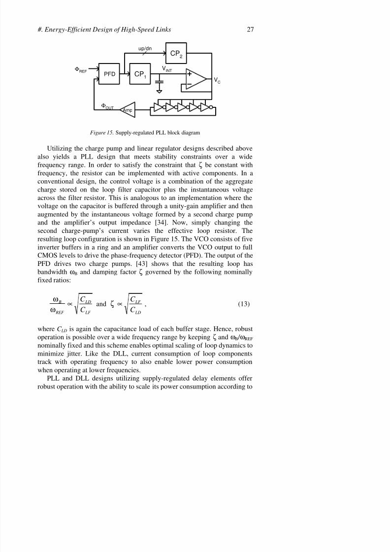
4.2 Adaptive-Supply Serial Links
Two examples of adaptive power-supply regulation applied to high-speed
interfaces can be found in the literature. A detailed description of a source-
synchronous parallel I/O that leverages the energy savings possible by
reducing the supply voltage along with clock rate is presented in [52]. In
addition to trading performance for energy reduction, the design obviates the
need for additional adjustment circuitry that scales certain properties of the
link proportionally with bit rate. For example, the loop bandwidths of PLLs
and DLLs, the slew rate of transmitters, and the bandwidth of the receiver all
track bit rate by exploiting the adaptive supply as a global bias voltage. Kim
and Horowitz extend this adaptive power-supply regulation technique to
serial links and solve several limitations that plague link circuitry operating
at low voltage levels. This section discusses some of the implementationdetails of adaptive supply serial links fully described in [28].
Serial links typically transmit more bits per clock period by exploiting
parallelism in the transmitter and receiver, and utilize multi-phase clocks to
provide fine timing information at lower frequencies [54]. As discussed in
section 3.2, transmitting multiple bits within a clock period not only
improves the performance, but also leads to further reduction in power
consumption if the supply voltage is dynamically scaled. At a given bit rate,
the power of the adaptive supply serial link drops quadratic to the
multiplexing rate, but at the cost of increased area. Thus, the combination of
parallelism and an adaptive supply allows one to trade area instead of
performance for lower power dissipation.
This section describes the various components required in a supply-
regulated serial link design with sub 1-V operation. Several challenges are
present as higher multiplexing rates are pursued. First, generating a large
number of clock phases at one place and then distributing them to multiple
I/O circuits becomes extremely difficult because strict matching between
clock paths is required to minimize static phase offsets. So instead, one can
generate the multi-phase clocks locally at each I/O circuit by exploiting the
coarse tuning voltage distributed by a global control loop. With adaptive
power-supply regulation, the adaptive power-supply regulator serves as this
global control loop and the adaptive supply voltage acts as the coarse tuning
voltage for the local clock generators. The clock generation and distribution
details are discussed in the Section 4.2.1. The second challenge is to design
8/6/2019 Wei_links_chapter02 Energy-Efficient Design of High-Speed Links
http://slidepdf.com/reader/full/weilinkschapter02-energy-efficient-design-of-high-speed-links 29/39
#. Energy-Efficient Design of High-Speed Links 29
the I/O circuits that can operate at low supply voltages. In order to achieve
power reduction with parallelism, one assumes that performance of I/O
circuitry scales with the supply voltage and tracks the delay of an inverter
[52]. Most conventional I/O circuits face problems as the supply voltage
approaches the threshold voltage of transistors since they are not purely
comprised of digital logic gates but contain some analog circuitry. Section
4.2.2 describes techniques to extend the lower supply limit down to 1.6*VTH.Lastly, to reduce pin count, typical serial links do not send clock information
along with the data, so the receive side of the transceiver must recover
timing information from the data stream. Both phase- and delay-locked loop
implementations are possible, but in the case of multi-phase clock recovery,
this example demonstrates that a phase-locked loop is more power and area
efficient. The rest of this section describes the implementation of the clock
recovery.
4.2.1 Multi-phase Clock Generation
Digital
Sliding
Controller
Reference VCO f
f ref
Adaptive
Supply, V VCO
CP
TX
Vctrl
Φ[m:1]
Adaptive Power-Supply Regulator
Multiphase Clock Genera tor PLL
PD
Data[m:1]
f ref
TX
Φ[m:1]
Data[m:1]
TX-PLL
RX
Ψ [m:1]
Data[m:1]
RX-PLL
Figure 16. Adaptive power-supply regulator and local multi-phase clock generators
Figure 16 illustrates the block diagram of multiple serial links with an
adaptive power-supply regulator and local clock generators. The adaptive
power-supply regulator adjusts the supply voltage using digital sliding
control [27] so that the reference VCO oscillates at the desired operating
frequency f ref . Sliding control is a nonlinear control mechanism widely used
in switching supplies and has superior stability and transient response to

8/6/2019 Wei_links_chapter02 Energy-Efficient Design of High-Speed Links
http://slidepdf.com/reader/full/weilinkschapter02-energy-efficient-design-of-high-speed-links 30/39
30 Chapter #
linear control [1]. Digital implementation of the sliding control has the
benefit that the critical path delay of the controller scales with the reference
frequency. Most linear and PWM-based controllers do not have this property
since the controller must operate at a fixed frequency [50]. This benefit
allows the digital sliding controller to operate off of the variable regulated
supply. Therefore, the power of the controller itself scales with the load
power and the controller power overhead remains a constant portion of thetotal power over a wide operation range. Implementation details and design
analysis of this power supply regulator are explained in [27].
The VCOs of local clock generator PLLs are identical to the reference
VCO inside the adaptive power-supply regulator. Thus, when the VCOs
operate at the adaptive supply, they are expected to oscillate at frequencies
very close to f ref . This way the adaptive supply is acting as a coarse tuning
voltage for the PLLs. The feedback adjustment of the local PLLs only need
to compensate for within-die variation and thus can have a narrow tuning
range (+/-15%). This eases the design of the PLL since noise on the control
voltage has less impact on the VCO clock jitter.
4.2.2 Low-Voltage Transmitter and Receiver
As the bit period reduces to less than 2 gate delays, it is difficult to
multiplex data on to an on-chip high-impedance node (although it can be
more power and area efficient [31]). Therefore, for high orders of
multiplexing, the off-chip low-impedance node of the transmitter output is
chosen. pMOS drivers transmit the signal referenced to ground since the
supply voltage is adaptively adjusted relative to the chip’s process and
operating conditions and thus can no longer be a common reference across
different chips. Each driver consists of two transistors in series and each
drives the output for a bit period, which is defined by the overlap of two
clocks with adjacent phases [55]. Predrivers qualify the clocks depending on
the data being transmitted.

8/6/2019 Wei_links_chapter02 Energy-Efficient Design of High-Speed Links
http://slidepdf.com/reader/full/weilinkschapter02-energy-efficient-design-of-high-speed-links 31/39
#. Energy-Efficient Design of High-Speed Links 31
F[n]
D[n] dclk[n]
qclk[n]
VV
V
F[n+1]
out
on-chiptermination
D[n] D[n+1]D[n-1]
dclk[n]
qclk[n]
out
V-Vth
-VthM1
M2V-Vth
-Vth
level-shiftingpredriver
tunable
delay
Figure 17. Low-voltage multiplexing transmitter
This conventional transmitter encounters a couple of problems as the
supply voltage reduces. First, the output swing drops rapidly as the supply
voltage approaches the threshold voltage, since the current of the pMOS
driver scales as (V-VTH)α. Second, the output pulse width narrows as supply
voltage drops due to the threshold voltage dependent switching points. Bothof these problems are related to the threshold voltage of the pMOS driver
and are limitations of the design in [52], which can be mitigated by making
the threshold voltage effectively zero. The transmitter illustrated in Figure 17
uses a level-shifting predriver that shifts its output voltage level down by a
threshold voltage VTH, so the gate voltage of the pMOS driver swings
between -VTH and V-VTH. Transistors M1 and M2 suppress leakage currents
when the pMOS drivers are barely off with the gate voltages at V-V TH. The
gate overdrive of the pMOS driver is now V instead of V-V TH, so the output
swing scales as Vα
with reasonable output swings even at low supplies. The
switching points are now independent of the supply and the output pulse-
width stays relatively constant across variable supply-voltage levels.
At the receiving end, parallel sets of current-integrating receivers de-multiplex the data stream. The receiving window of each receiver is defined
by a set of multi-phase clocks. For high-frequency noise rejection, each
front-end of the receiver integrates the signal during a bit period [41]. This
implementation avoids voltage headroom issues associated with low-voltage
operation by boosting the supply voltage to the integrating receiver circuitry
and eliminating the sample and hold circuitry found in the original design.
Lastly, a modified, comparator circuit that can operate at sub-1V supply
levels amplify the integrated signal to full logic levels.

8/6/2019 Wei_links_chapter02 Energy-Efficient Design of High-Speed Links
http://slidepdf.com/reader/full/weilinkschapter02-energy-efficient-design-of-high-speed-links 32/39
32 Chapter #
4.2.3 Clock-Recovery PLL
RXPD
DataRX
VCO
Edge
Detect
5
5
enable
dnup
Vctrl
Ψ[4:0]
cycle-slipdetector
lockdetector
rst
frequencysweeper
up
charge pump
dn
Figure 18. Clock recovery PLL
In the absence of a dedicated parallel clock signal, each serial link must
recover timing information from the data stream. Figure 18 illustrates the
clock recovery PLL implemented. A duplicate set of data receivers sampling
the edges instead of the center of the data eye enables phase detection, but
provides only binary information on the phase. Hence, PLLs with binary
phase-detectors are bang-bang controlled [49] and they must have low loop
bandwidths to minimize dither jitter when locked. This low bandwidth
results in a very narrow frequency range (+/-2%) that the PLL can lock. So
frequency acquisition aid is necessary to guide the VCO frequency to fall
within the lock-in range. However, since the VCO frequency is coarsely
tuned by the adaptive supply and already close to the desired frequency,
simple frequency sweeping can be used [17]. During preamble mode, the
transmitter sends a full-transition signal (10101010 bit pattern) and the
receiver can detect cycle slipping when consecutive 1’s and 0’s are received.
The frequency sweeper initializes the control voltage VCTRL to the highest
value and then steps it down whenever cycle slipping is detected. As the
loop approaches lock, cycle slipping happens less frequently and the phase
acquisition loop finally pulls the loop into lock.
Although DLL-based per-pin clock recovery is also possible, it requires
additional overhead to generate multiple phases of the clock (either multiple
mux/intepolator paths or a 180-degree delay-line) [44][52]. PLL-based clock
recovery circuits can generate multiphase clocks from the VCOs, and
therefore are more power and area efficient compared to its DLL
counterpart.

8/6/2019 Wei_links_chapter02 Energy-Efficient Design of High-Speed Links
http://slidepdf.com/reader/full/weilinkschapter02-energy-efficient-design-of-high-speed-links 33/39
#. Energy-Efficient Design of High-Speed Links 33
4.3 Low-Power Area-Efficient Hi-Speed I/O Circuit
Techniques
In addition to adaptive power-supply regulation, other examples of low-
power I/O circuit techniques to implement high-speed serial links can be
found in the literature. Lee, et al investigate three techniques to achieve
small area and low power in [31] and [32], and demonstrate a high-speedlink, implemented in a 0.25-µm CMOS technology, that operates at 4-Gb/s
while dissipating 127mW. This link design example also multiplexes several
bits within a clock period to achieve high bit rates, but instead of
multiplexing at the transmitter output, multiplexing is performed further
back in the transmit path in order to reduce clock energy. In order to attain
the speed necessary in the circuitry following the mux point, lower voltage
swings in the signal paths are used. The design also implements a DLL with
supply-regulated inverters to generate low-jitter clocks while reducing power
consumption. Clock recovery is achieved with a dual-loop design similar to
the design described in Section 2.4. Lastly, a capactively-trimmed receiver
enables reliable operation at very low signal levels by compensating for
device offsets. Since the DLL design used for clock generation is similar tothe supply-regulated designs previously described in this section, we will
concentrate on the design of the transmitter and receiver.
4.3.1 Transmitter
φi
φi-1
di
φi
φi-1
di
50Ω
18
φ1
φ2
φ3
φ0
Figure 19. Differential transmitter with sub-clock period bit times
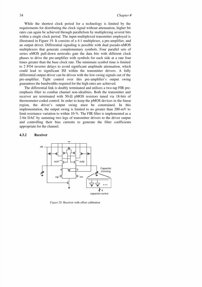
8/6/2019 Wei_links_chapter02 Energy-Efficient Design of High-Speed Links
http://slidepdf.com/reader/full/weilinkschapter02-energy-efficient-design-of-high-speed-links 34/39
34 Chapter #
While the shortest clock period for a technology is limited by the
requirements for distributing the clock signal without attenuation, higher bit
rates can again be achieved through parallelism by multiplexing several bits
within a single clock period. The input-multiplexed transmitter employed is
illustrated in Figure 19. It consists of a 4:1 multiplexer, a pre-amplifier, and
an output driver. Differential signaling is possible with dual pseudo-nMOS
multiplexers that generate complementary symbols. Four parallel sets of series nMOS pull-down networks gate the data bits with different clock
phases to drive the pre-amplifier with symbols for each side at a rate four
times greater than the base clock rate. The minimum symbol time is limited
to 2 FO4 inverter delays to avoid significant amplitude attenuation, which
could lead to significant ISI within the transmitter drivers. A fully
differential output driver can be driven with the low-swing signals out of the
pre-amplifier. Tight control over this pre-amplifier’s output swing
guarantees the bandwidths required for the high rates are achieved.
The differential link is doubly terminated and utilizes a two-tap FIR pre-
emphasis filter to combat channel non-idealities. Both the transmitter and
receiver are terminated with 50-Ω pMOS resistors tuned via 18-bits of
thermometer-coded control. In order to keep the pMOS devices in the linearregion, the driver’s output swing must be constrained. In this
implementation, the output swing is limited to no greater than 200-mV to
limit resistance variation to within 10-%. The FIR filter is implemented as a
2-bit DAC by summing two legs of transmitter drivers to the driver output
and controlling their bias currents to generate the filter coefficients
appropriate for the channel.
4.3.2 Receiver
clk
inp inn
outn outp
a b Capacitortrimming
4
capacitor control
Figure 20. Receiver with offset calibration
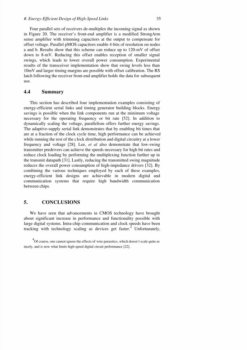
8/6/2019 Wei_links_chapter02 Energy-Efficient Design of High-Speed Links
http://slidepdf.com/reader/full/weilinkschapter02-energy-efficient-design-of-high-speed-links 35/39
#. Energy-Efficient Design of High-Speed Links 35
Four parallel sets of receivers de-multiplex the incoming signal as shown
in Figure 20. The receiver’s front-end amplifier is a modified StrongArm
sense amplifier with trimming capacitors at the output to compensate for
offset voltage. Parallel pMOS capacitors enable 4-bits of resolution on nodes
a and b. Results show that this scheme can reduce up to 120-mV of offset
down to 8-mV. Reducing this offset enables reception of smaller signal
swings, which leads to lower overall power consumption. Experimentalresults of the transceiver implementation show that swing levels less than
10mV and larger timing margins are possible with offset calibration. The RS
latch following the receiver front-end amplifier holds the data for subsequent
use.
4.4 Summary
This section has described four implementation examples consisting of
energy-efficient serial links and timing generator building blocks. Energy
savings is possible when the link components run at the minimum voltage
necessary for the operating frequency or bit rate [52]. In addition to
dynamically scaling the voltage, parallelism offers further energy savings.The adaptive-supply serial link demonstrates that by enabling bit times that
are at a fraction of the clock cycle time, high performance can be achieved
while running the rest of the clock distribution and digital circuitry at a lower
frequency and voltage [28]. Lee, et al also demonstrate that low-swing
transmitter predrivers can achieve the speeds necessary for high bit rates and
reduce clock loading by performing the multiplexing function further up in
the transmit datapath [31]. Lastly, reducing the transmitted swing magnitude
reduces the overall power consumption of high-impedance drivers [32]. By
combining the various techniques employed by each of these examples,
energy-efficient link designs are achievable in modern digital and
communication systems that require high bandwidth communication
between chips.
5. CONCLUSIONS
We have seen that advancements in CMOS technology have brought
about significant increase in performance and functionality possible with
large digital systems. Intra-chip communication and clock speeds have been
tracking with technology scaling as devices get faster.4
Unfortunately,
4Of course, one cannot ignore the effects of wire parasitics, which doesn’t scale quite as
nicely, and is now what limits high-speed digital circuit performance [22].

8/6/2019 Wei_links_chapter02 Energy-Efficient Design of High-Speed Links
http://slidepdf.com/reader/full/weilinkschapter02-energy-efficient-design-of-high-speed-links 36/39
36 Chapter #
package and channel mediums for inter-chip communications have not been
advanced at the same rate. Therefore, high-speed signaling techniques were
developed to alleviate the communication bandwidth bottleneck. As seen for
digital systems where the pursuit of low-power, energy-efficient designs has
become just as significant as the pursuit of raw speed and performance,
designers are looking for new and innovative ways to build energy-efficient
links. This Chapter has provided a brief overview of link design andpresented various trade-offs and techniques for energy-efficient operation.
Further research and development in low-power circuit techniques,
packaging, and interconnect technology should continue to improve energy
efficiency of links. However, we can again learn from the digital systems
designers who have been able to find lower-power implementations by re-
visiting the system from an architectural and algorithmic level [18].
Similarly, investigating alternative modulation schemes and communication
methods may offer other innovative energy-efficient link solutions.
References
[1] F. Bilaovic et al, “Sliding modes in electrical machines control systems,” IEEE Int’l
Symp. on Industrial Electronics Conference Proceedings, 1992, pp. 73-78.
[2] G. Besten, “Embedded low-cost 1.2Gb/s inter-IC serial data link in 0.35mm
CMOS,” IEEE Int’l Solid-State Circuits Conf. Dig. Tech. Papers, Feb. 2000, pp.
250-251.
[3] T. Burd et al, “A dynamic voltage scaled microprocessor system,” IEEE Int’l Solid-
State Circuits Conf. Dig. Tech. Papers, Feb. 2000, pp. 294-295.
[4] A. P. Chandrakasan et al, “Data driven signal processing: An approach for energy
efficient computing,” IEEE Int’l Symposium on Low Power Electronics and Design
Dig. Tech. Papers, Aug. 1996, pp. 347-352.
[5] A.P. Chandrakasan et al, Low Power Digital CMOS Design. Norwell, MA: Kluwer
Academic, 1995.
[6] K. -Y. K. Chang et al, “A 0.4-4Gb/s CMOS quad transceiver cell using on-chip
regulated dual-loop PLLs,” IEEE Symposium on VLSI Circuits, accepted forpublication June 2002.
[7] W.J. Dally et al, Digital Systems Engineering, Cambridge University Press, 1998.
[8] W.J. Dally et al, “Transmitter equalization for 4-Gbps signalling” IEEE Micro, Jan.-Feb. 1997. vol. 17, no. 1, p. 48-56
[9] A. DeHon et al, “Automatic impedance control,” 1993 IEEE Int’l Solid-State
Circuits Conf. Dig. Tech. Papers, p. 164-5, Feb. 1993.
[10] D. Dobberpuhl, “The design of a high performance low power microprocessor,”
IEEE Int’l Symposium on Low Power Electronics and Design Dig. Tech. Papers,
Aug. 1996, pp. 11-16.

8/6/2019 Wei_links_chapter02 Energy-Efficient Design of High-Speed Links
http://slidepdf.com/reader/full/weilinkschapter02-energy-efficient-design-of-high-speed-links 37/39
#. Energy-Efficient Design of High-Speed Links 37
[11] K. Donnelly et al, “A 660 MB/s interface megacell portable circuit in 0.3um-0.7mm
CMOS ASIC,” IEEE Int’l Solid-State Circuits Conf. Dig. Tech. Papers, pp. 290-
291, Feb 1996.
[12] R. Farjad-Rad et al, "A 0.3-µm CMOS 8-GS/s 4-PAM Serial Link Transceiver",
IEEE Symposium on VLSI Circuits Dig. Tech. Papers, p. 41-44.
[13] A. Fieldler et al, “A 1.0625 Gbps transceiver with 2X oversampling and transmit
pre-emphasis,” IEEE Int’l Solid-State Circuits Conf. Dig. Tech. Papers, Feb. 1997,
pp. 238-239.[14] M. Fukaishi et al, “A 20Gb/s CMOS multi-channel transmitter and receiver chip set
for ultra-high resolution digital display,” IEEE Int’l Solid-State Circuits Conf. Dig.
Tech. Papers, Feb 2000, pp. 260-261.
[15] P. Galloway et al, “Using Creative Silicon Technology to Extend the useful like of
backplane and card substrates at 3.125 Gbps and Beyond,” High-Performance
System Design Conference, 20001.
[16] F.M. Gardner, “Charge-pump phase-lock loops,” IEEE Transactions on
Communications, vol. 28, no.11, Nov. 1980, pp. 1849-1858.
[17] F.M. Gardner, “Frequency granularity in digital phase-lock loops,” IEEE
Transactions on Communications, vol. 44, no. 6, June 1996, pp. 749-758.
[18] L. Geppert, “Transmeta’s magic show [microprocessor chips],” IEEE Spectrum,
vol. 37, no. 5, May 2000, pp. 26-33.
[19] Y.M. Greshishchev et al, “A fully integrated SiGe receiver IC for 10Gb/s data rate,”
IEEE Int’l Solid-State Circuits Conf. Dig. Tech. Papers, Feb. 2000, pp. 52-53.[20] R. Gu et al, “ 0.5-3.5Gb/s low-power low-jitter serial data CMOS transceiver,”
IEEE Int’l Solid-State Circuits Conf. Dig. Tech. Papers, Feb 1999, pp. 352-353.
[21] V. Gutnik et al, An efficient controller for variable supply voltage low power
processing,” IEEE Symposium on VLSI Circuits Dig. Tech. Papers, June 1996, pp.
158-159.
[22] R. Ho et al, “Interconnect scaling implications for CAD,” IEEE/ACM Int’l Conf.
Computer Aided Design Dig. Tech. Papers, Nov. 1999, pp. 425-429.
[23] M. Horowitz, “Low power processor design using self-clocking,” Workshop on
Low-Power Electronics, 1993.
[24] M. Horowitz et al, “High-speed electrical signalling: Overview and limitations,”
IEEE Micro, vol. 18, no. 1, Jan.-Feb. 1998, pp.12-24.
[25] H. Johnson, “Multi-level signaling,” DesignCon, Feb. 2000.
[26] M. Johnson, “A variable delay line PLL for CPU-coprocessor synchronization,”
IEEE Journal of Solid-State Circuits, vol. 23, no. 5, Oct. 1988, pp. 1218-1223.[27] J. Kim et al, “A digital adaptive power-supply regulator using sliding control,”
IEEE Symposium on VLSI Circuits Dig. Tech. Papers, June 2001.
[28] J. Kim et al ,“Adaptive supply serial links with sub-1V operation and per-pin clock
recovery,” IEEE Int’l Solid-State Circuits Conf. Dig. Tech. Papers, Feb 2002.
[29] P. Larsson, “Measurement and analysis of PLL jitter caused by digital switching
noise,” IEEE Journal of Solid-State Circuits, July 2001, vol. 37, no. 7, pp. 1113-
1119.
[30] B. Lau et al, “A 2.6Gb/s multi-purpose chip to chip interface,” IEEE Int’l Solid-
State Circuits Conf. Dig. Tech. Papers, Feb 1998, pp. 162-163.
[31] M. -J. E. Lee et al, “Low-power area efficient high speed I/O circuit techniques,”
IEEE Journal of Solid-State Circuits, vol. 35, Nov. 2000, pp. 1591-1599.
[32] M. -J. E. Lee et al, “An 84-mW 4-Gb/s clock and data recovery circuit for serial
link applications,” IEEE Symposium on VLSI Circuits Dig. Tech. Papers, June
2001.

8/6/2019 Wei_links_chapter02 Energy-Efficient Design of High-Speed Links
http://slidepdf.com/reader/full/weilinkschapter02-energy-efficient-design-of-high-speed-links 38/39
38 Chapter #
[33] P. Maken, M. Degrauwe, M. Van Paemel and H. Oguey, “A voltage reduction
technique for digital systems,” IEEE Int’l Solid-State Circuits Conf. Dig. Tech.
Papers, Feb. 1990, pp238-239.
[34] J.G. Maneatis, “Low-Jitter process independent DLL and PLL based on self-biased
techniques,” IEEE Journal of Solid-State Circuits, vol. 28, no. 12, Dec. 1993.
[35] J.G. Maneatis, “Precise delay generation using coupled oscillators,” Ph.D.
dissertation , Stanford University, Stanford, CA, June 1994.
[36] M. Mansuri et al, “Jitter optimization based on phase-locked-loop designparameters,” IEEE Int’l Solid-State Circuits Conf. Dig. Tech. Papers, Feb. 2002.
[37] J.P. Mattia et al, “A 1:4 demultiplexer for 40Gb/s fiber-optic applications,” IEEE
Int’l Solid-State Circuits Conf. Dig. Tech. Papers, Feb. 2000, pp. 64-65.
[38] L. Nielsen et al, “Low-power operation using self-timed circuits and adaptive
scaling of supply voltage,” IEEE Trans. VLSI Systems., vol. 2, pp 391-397, Dec
1994.
[39] J. Proakis, M. Salehi, Communications Systems Engineering, Prentice Hall, New
Jersey, 1994.
[40] Reese et al “A phase-tolerant 3.8 GB/s data-communication router for muli-
processor super computer backplane,” IEEE Int’l Solid-State Circuits Conf. Dig.
Tech. Papers, pp. 296-297, Feb. 1994.
[41] S. Sidiropoulos et al, “A 700-Mb/s/pin CMOS signalling interface using current
integrating receivers,” IEEE Journal of Solid-State Circuits, May 1997, pp. 681-
690.[42] S. Sidiropoulos et al, “A CMOS 500Mbps/pin synchronous point to point
interface,” IEEE Symposium on VLSI Circuits, June 1994.
[43] S. Sidiropoulos et al, “Adaptive bandwidth DLL’s and PLL’s using regulated-
supply CMOS buffers,” IEEE Symposium on VLSI Circuits Dig. Tech. Papers, June
2000.
[44] S. Sidiropoulos and M. Horowitz, “A semi-digital dual delay-locked loop,” IEEE
Journal of Solid-State Circuits, Nov. 1997, pp. 1683-1692.
[45] J. Sonntag et al, “An adaptive PAM-4 5 Gb/s backplane transceiver in 0.25um
CMOS,” IEEE Custom Integrated Circuits Conference, to be published 2002.
[46] A. J. Stratakos, “High-efficiency low-voltage DC-DC conversion for portable
applications,” Ph.D. dissertation, University of California, Berkeley, CA, Dec.
1998.
[47] K. Suzuki et al, “A 300 MIPS/W RISC core processor with variable supply-voltage
scheme in variable threshold-voltage CMOS,” Proceedings of the IEEE Custom Integrated Circuits Conference, May 1997, pp. 587-590.
[48] T. Tanahashi et al, “A 2Bb/s 21CH low-latency transceiver circuit for inter-
processor communication,” IEEE Int’l Solid-State Circuits Conference Dig. Tech.
Papers, Feb. 2001, pp. 60-61.
[49] R.C. Walker et al “A two-chip 1.5-GBd serial link interface,” IEEE Journal of
Solid-State Circuits, vol. 27, no. 12, Dec. 1992, pp. 1805-1811.
[50] G. Wei et al “A low power switching power supply for self-clocked systems,” IEEE
Symposium on Low Power Electronics, Oct. 1996, pp. 313-317.
[51] G. Wei et al, “A full-digital, energy-efficient adaptive power supply regulator,”
IEEE Journal of Solid-State Circuits, vol. 34, no. 4, April 1999, pp. 520-528.
[52] G. Wei et al, “A variable-frequency parallel I/O interface with adaptive power-
supply regulation,” IEEE Journal of Solid-State Circuits, vol. 35, no. 11, Nov.
2000, pp. 1600-1610.
8/6/2019 Wei_links_chapter02 Energy-Efficient Design of High-Speed Links
http://slidepdf.com/reader/full/weilinkschapter02-energy-efficient-design-of-high-speed-links 39/39
#. Energy-Efficient Design of High-Speed Links 39
[53] D. Weinlader et al, “An eight channel 36Gample/s CMOS timing analyzer,” IEEE
Int’l Solid-State Circuits Conf. Dig. Tech . Papers, Feb. 2000, pp. 170-171.
[54] C. -K. Yang, “Design of high-speed serial links in CMOS,” Ph.D. dissertation,
Stanford University, Stanford, CA, Decemeber 1998.
[55] K. Yang, “A scalable 32Gb/s parallel data transceiver with on-chip timing
calibration circuits,” IEEE Int’l Solid-State Circuits Conf. Dig. Tech. Papers, Feb.
2000, pp. 258-259.
[56] E. Yeung et al, “A 2.4Gb/s/pin simultaneous bidirectional parallel link with per pinskew compensation,” IEEE Int’l Solid-State Circuits Conf. Dig. Tech. Papers, Feb.
2000, pp. 256-257.
[57] Zerbe et al, “A 2Gb/s/pin 4-PAM parallel bus interface with transmit crosstalk
cancellation, equalization, and integrating receivers,” IEEE Int’l Solid-State Circuits
Conf. Dig. Tech. Papers, Feb. 2001, pp. 66-67.