Embed Size (px)
Citation preview

Webinar: SEMI Americas
Quarterly Update to Members
February 2013: Q1 Update Ray Morgan, Director of Membership

Agenda
• SEMI Update • ISS 2013 - Highlights and Insights • SEMI Programs - Chapter Report • Member Spotlight – Applied Materials • Q&A • Closing Remarks

Today’s Presenters
• Ray Morgan, Director of Outreach and Membership, SEMI Americas – SEMI Activity Update & ISS Highlights & Insights – Contact: [email protected], 408.943.7047
• Lin Tso, Sr. Manager, Programs, SEMI Americas – Chapter Report / New Regional Programs – Contact: [email protected], 408.943.7920
• John Grisham, Director, Applied Materials, SEMI Pacific Northwest Chapter Chair – Applied Introduction & Success Story of New Workforce
Development Program

Agenda
• SEMI Update – SEMI Membership • ISS 2013 - Highlights and Insights • SEMI Programs - Chapter Report • Member Spotlight – Applied Materials • Q&A • Closing Remarks

SEMI & Membership
Jan, 2013

About SEMI SEMI is a global organization representing 1,850+ member companies who innovate, manufacture, and supply the processes, tools, technologies, and materials that enable advanced microelectronics for: • Semiconductors │Photovoltaics │ High-brightness LEDs • MEMS │ Plastic │ Organic/flexible electronics │Display
SEMI exists to • Advance the growth and prosperity of the global
microelectronics industry • Help and support our members' technology and business
development worldwide • Support innovation that enables faster, more powerful, and
more affordable electronic devices that enrich people's lives SEMI Supports our Members through: • Trade shows & Conferences • Standards & Information/market data reports • Initiatives/collective action & Advocacy • Partnerships

SEMI Global Membership
CHINA 275 Companies
EUROPE 279 Companies
INDIA 9 Companies
JAPAN 378 Companies
KOREA 201 Companies
AMERICAS 466 Companies
SINGAPORE 37 Companies
TAIWAN 233 Companies
1,868 Members As of December 2012

International Board of Directors
Driven by Members
Regional Advisory Boards
Americas Europe Southeast
Asia India China Taiwan Japan Korea
Special Interest Groups
• EHS • Silicon Manufacturers • Chemicals & Gases • Public Policy • Secondary Equipment • Test • Logistics
Programs Committees
• Packaging • Lithography • Process Control • Wafer Conditioning • Test • LED • PV • Event Advisory
Standards Committees
• EHS • Physical Interface • Chemicals & Gases • Equipment Communication • Facilities • Metrics • Silicon Wafer • 3DS-IC • PV • LED

WWW.SEMI.ORG – Learn More

Agenda
• SEMI Update – Global Update • ISS 2013 - Highlights and Insights • SEMI Programs - Chapter Report • Member Spotlight – Applied Materials • Q&A • Closing Remarks

2012 Membership Survey Overall Satisfaction Rating
69%70%
62%68%
86%
56%
71%
91% 89% 90% 93% 95% 95% 93%93% 94% 94% 94% 96%
80%
94%94%89%
96% 93% 92%96% 99%
Total Japan North America Europe China Korea SE Asia
2009
2010
2011
2012
Overall Satisfaction with SEMI Among Members - Percent Above Acceptable and Acceptable - I am pleased to report that the
annual SEMI Customer Satisfaction Survey shows member satisfaction reached its highest level since the annual rating system was instituted eight years ago. Overall, 94 percent of the respondents rated satisfaction with SEMI as Acceptable or Above Acceptable, improving in nearly all regions. Member satisfaction was nearly identical among companies of different revenue levels and industry segments. One of the most important outcomes confirmed by the annual study was the critical importance of key SEMI functional areas to member satisfaction, especially in the areas of exhibitions, standards, global advocacy, market data, and membership. Denny McGuirk, President and CEO, SEMI
About the Survey: The survey was conducted in English, Japanese, Korean, and both simplified and traditional Chinese. Feedback was collected from nearly 1,000 members and provides a 2.7 percent margin of error with 95 percent confidence. The survey was administered and analyzed by Quality Resources Partners, a market research firm with experience in the microelectronics industry.

Silicon Wafer Shipment Forecast 2012 October projections polished and epitaxial silicon shipments to reach 8,901 million and 9,400 million square inches in 2013, and 9,965 million square inches in 2014.
Semiconductor Equipment Outlook 2012 December projections for new semiconductor manufacturing equipment orders $ 38.2 billion. Slight decline by 2% in 2013. In 2014, growth will resume.
Semiconductor Equipment Book-to-Bill December 2012 Statistics Oct $742.8 million in orders; book-to-bill ratio of 0.75 Nov $718.6 million in orders; book-to-bill ratio of 0.79 Dec $924.1 million in orders; book-to-bill ratio of 0.92 (prelim)
Semiconductor Materials Market Estimated $47.7 billion in 2012 and grow to $49.8 billion by 2013.
Worldwide Semiconductor Equipment Billings Worldwide semiconductor manufacturing equipment billings reached $9.06 billion in the third quarter of 2012. The billings figure is 12% percent lower than Q2 2012 and 15% lower than the same quarter a year ago.
All data is as of December 2012 and is US$ if not otherwise noted
http://www.semi.org/MarketInfo

International Technology Partners Conference (ITPC) 2012 (November) 27th International Technology Partners Conference (ITPC). Industry leaders from all over the globe convened to discuss and collaborate on global manufacturing, technology and trade issues for the semiconductor and adjacent industries. SEMICON Japan 2012 and PVJapan 2012 (December) December 5-7 34,145. Over 850 companies exhibited at the combined show. Hot topics included, Power Semiconductors, 3D-ICs, Printed Electronics, 450mm, EUV, and MEMS. PVJapan 2012 (December) PVJapan 2012 was held concurrently with SEMICON Japan, featuring 196 exhibiting companies and total attendance of 11,000 from eight countries.
SEMICON Europa 2012 (October) Dresden, Germany. With more than 4,100 visitors and exhibitors in attendance and over 340 companies exhibiting Plastic Electronics 2012 (October) Co-located with SEMICON Europa for the third consecutive year, Plastic Electronics 2012. The event covered OLEDs (for Display and Lighting), Flexible and Organic PV, integrated smart systems and focused on transferring technology into volume manufacturing. Strategic Materials Conference (SMC) 2012 (October) Held at SEMI HQ in San Jose,CA, this event is the only conference dedicated to exploring the synergies, trends and business opportunities in advanced electronic materials. Over 130 attended the conference PV Taiwan 2012 (October) 8,000+ visitors from 60 countries. A total of 119 one-on-one trade meetings were arranged for 40 foreign buyers during the 3-day show which was expected to generate more than US$ 120 million in immediate and future business deals. China LED Manufacturing Conference 2012 (October) On October 19 in Shanghai, co-organizers SEMI and Swagelok presented the 2012 China LED Manufacturing Conference.
Global Expositions and Events

Arizona Breakfast Forum: In Chandler, Arizona on October 11, Microchip Technology Inc. hosted the Breakfast Forum with speakers from AZ Technology Council, OEM Group, IC Insights, and Microchip Technology. Over 80 attended the event.
SEMI Professional Development Seminar: In Corvallis, Oregon on October 26, over 65 STEM major students participated in the "Jobs in the Micro- and Nano-Electronics Industry: Connecting Students to Industry" half-day event that was co-sponsored by SEMI, Oregon State University, participating SEMI member companies, Oregon Nanoscience and Microtechnologies Institute, and Pacific Northwest National Laboratory.
SEMI Austin Annual Industry Outlook Forum: In Austin, Texas on October 30, the annual SEMI Austin Industry Outlook Forum featured speakers from Gartner, IC Insights, Perryman Group, SEMATECH, Stratfor Global Intelligence, and Tokyo Electron. Over 85 people participated in the event.
SEMI Pacific Northwest Dinner: In Portland, Oregon on November 8, SEMI presented "Advanced Electronic Materials: Highlights, Challenges, and Outlook." Over 90 attended the event which featured presentations from Air Products, FEI, Intel, and Techcet Group.
Americas Regional Events Outlook on the Semiconductor Manufacturing Industry: On December 11, Lara Chamness and Chris Dieseldorff, both from the Industry Research and Statistics group at SEMI, presented outlooks at the webinar.
Opportunities in the Turbulent Photovoltaic Equipment Market: On December 13, Fatima Toor from Lux Research presented at the webinar.
SEMI Americas Quarterly Update for Members (Nov 14): Ray Morgan moderated the webinar. The "Member Spotlight" was on Entegris with guest speaker Paul Rosenfeld from the Microenvironments Division. Dan Tracy, SEMI Industry Research and Statistics, presented a Market Update/Fab Activity (with 450mm).
WEBINARS

3DS-IC In Ballot: • Specification for Glass Carrier Wafers for 3DS-IC
Application • Test Method for Measuring Warp, Bow and TTV on
Silicon and Glass Wafers Mounted on Wire Grids by Automated Non-Contact Scanning using Laser Scanning Interferometry
Proposals • Guide for Incoming/Outgoing Quality Control and
Testing Flow for 3DS-IC Products3D-IC Working Group News • Study Group meeting was held on December 6 in
conjunction with SJ2012. 30 people participated. Current global activities were introduced and future directions discussed. Standardization on thin wafer bending strength measurement is candidate for future activities.
HIGH-BRIGHTNESS LED In Ballot • Specifications for Sapphire Wafers Intended for Use for
Manufacturing High Brightness-Light Emitting Diode Devices
PHOTOVOLTAICS In Ballot – Specifications for: • Package protection technology for PV Modules • Test Method for the content of Vinyl Acetate (VA) in Ethylene-Vinyl
Acetate (EVA) applied in PV modules --Thermal Gravimetric Analysis (TGA)
• Impurities in Polyethylene Packaging Materials for Polysilicon Feedstock • Quasi-monocrystalline Silicon Wafers used in Photovoltaic Solar Cells • Anti-reflective-coated Glass, Used In Crystalline Silicon Photovoltaic
Modules PV Automation Published - Specification SEMI PV35-1012 - Horizontal Communication Between Equipment for Photovoltaic Fabrication System (tool to tool in flow communications) PV Materials Proposals • Test Method for Measurement of Cracks in PV Silicon Wafers in PV
Modules by Laser Scanning New • Test Method for the Measurement of Oxygen Concentration in PV Silicon
Materials for Silicon Solar Cells by Inert Gas Fusion Infrared Detection Method; PV43-0113.
• Test Method for In-Line Measurement of Waviness of PV Silicon Wafers by a Light Sectioning Technique Using Multiple Line Segments. PV42-0113
• Specification for Orientation Fiducial Marks for PV Silicon Wafers
Emerging Standard Segment Areas Shown (Q4 2012) http://www.semi.org/Standards

SEMI Europe addresses national governments on the importance of III-V compounds Key Points; SEMI Europe addressed a meeting of national ministries to explain how III-V compounds are irreplaceable when it comes to delivering the fast, smart and efficient devices Distributed PV Application and Commercialization Forum Key Points: Stakeholder meetings in China to discuss PV policy incentives, industry upgrades, techno-economy, management and market mechanisms. SEMI Applauds Approval of Permanent Normal Trade Relations (PNTR) for Russia Key Points: In December, SEMI praised Congressional leadership as the U.S. Senate passed legislation (92-4 vote) to normalize trade relations with Russia. SEMI North American Advisory Board Commits to Corporate Tax Reform Principles Key Points: Lower top corporate tax to be closer to the average rate of 25.1% for industrialized nations. Retention of innovation polices like the R&D tax credit. Shift to a territorial tax system. SEMI Submits Comments on Renewable Energy Trade to U.S. International Trade Commission. Key Points: Supply chain importance, impact on jobs, elimination of tarrifs. SEMI Export Control Working Group Holds Inaugural Meeting Key Points: The ECWG serves to monitor U.S. policies governing the trade of dual-use goods. The group openly advocates for policies which promote innovation and growth within the industry, while supporting national security concerns.
SEMI Publishes Regulatory Summary of the New U.S. Conflict Minerals Regulation Key Point: SEMI Conflict Minerals Working Group reviewed and provided feedback to new regulatory language on SEC requirements for U.S. and foreign companies to report on the conflict-minerals content of their products. SEMI Hosts EHS Regulatory Compliance Seminar at SEMICON Japan 2012 Key Point: At SEMICON Japan, SEMI held a regulatory compliance seminar. Topics included the U.S. Conflict Minerals Legislation and changes to the European RoHS Regulation. Global Environment Symposium at SEMICON Japan 2012 Key Point: At SEMICON Japan seminar. Topics included energy and water conservation and green house gas (GHG) emission abatement. EHS Technical Content Shared at SEMI China LED Manufacturing Workshop Key Point: SEMI hosted a technical seminar at full-day technical and business seminar in Shanghai on EHS and manufacturing issues. CAST Elects New Leadership to Address Future of Semiconductor Test In November, the Collaborative Alliance for Semiconductor Test (CAST), a SEMI special interest group, elected new leadership to advance their mission to develop, accelerate and support industry-wide advances in semiconductor test
www.semi.org/press

Preview & Highlights

SEMICON West
SEMICON West is the largest
microelectronics manufacturing
exposition in North America.
Engineers, fab managers, and executives from across
the microelectronics industry and around the world
recognize SEMICON West as the premier forum for
discovering new technologies, sourcing solutions,
and connecting with suppliers and partners who can
move their innovations forward.
Participants will find key customers and buyers from
across the microelectronics supply chain— from
materials to final manufacturing and semiconductors
to high brightness LEDs— who will help you grow
your business. Intersolar North America is co-located with
SEMICON West.


SEMICON West Visitor Profile Total 2012 Verified Attendance = 17,800
Influential Buyers 70% of visitors say that what they see and who they meet at SEMICON West influences their buying decisions over the next 12 months.
2013 Technology Themes— The Power of [X]
[Wafer Processing] – Manufacturing nonplanar
transistors – Advanced lithography – 450mm wafer processing – Advanced materials and
processes
[Productivity Innovation] – Productivity technology for
existing fabs – Equipment and materials
management – Secondary equipment and
solutions
[Test and Packaging] – Semiconductor test strategies – Probe card technology – Trends and opportunities in 3D IC – Advanced packaging materials and
technologies
[Extreme Electronics] – Lab-to-fab: R&D to high-volume
manufacturing – MEMS manufacturing and
technology – High Brightness LED manufacturing – Printed and flexible electronics

What’s New for 2013
• Increased focus on R&D & Innovation • Silicon Innovation Forum
• R&D Keynote Panel Wed. morning with SEMATECH, CEA-Leti, and imec
• “Lab to Fab” session in Extreme Electronics
• Themed networking on the show floor
• Fab Productivity, LED, Advanced Packaging
• Bulls and Bears Investor Panel
• Regional advisory boards get-together
• Global intellectual property event
• SEMI Executive Panel

THE FORUM The Silicon Innovation Forum (SIF) will address these global dynamics and showcase current, emerging and potential solutions to accelerating R&D and supply chain innovation in this newly-constrained world. The Forum will provide a stage for new and emerging innovators, industry leaders, strategic investors, and venture capitalists to discuss the needs and requirements of the industry’s innovation engine, and provide insights into technology, capital, partnership, and collaboration strategies necessary for mutual success. The Forum will highlight both short-term business opportunities for early /mid-stage companies, R&D entrepreneurs from larger companies, and other industry innovators—while addressing long-term structural changes to the industry necessary to foster a healthy innovation pipeline.
Conference
Exhibit Showcase
http://www.semiconwest.org/sif

Feb 24-26: ISS Europe 2013 (Milan, Italy)
Mar 10-12: 7th PV Fab Managers Forum 2013 (Berlin, Germany)
Mar 19-21: SEMICON China 2013 (Shanghai, China)
Mar 19-21: FPD China 2013 (Shanghai, China)
Mar 19-21: SOLARCON China 2013 (Shanghai, China)
Mar 20: SEMI Northeast Forum (Billerica, MA)
Mar 31-Apr 4: SEMI North America Standards Spring Meetings (San Jose, CA)
May 7-9: SEMICON Singapore 2013 (Marina Bay Sands, Singapore)
May 14-16: ASMC 2013 (Saratoga Springs, NY)
Jun 5-6: SEMICON Russia 2013 (Moscow, Russia)
Jun 19-21: Intersolar Europe 2013 PV Prod & Technologies (Munich, Germany)
Jul 9-11: SEMICON West 2013 (San Francisco, CA)
Jul 9-11: Intersolar N. America 2013: PV Prod & Technologies (San Francisco, CA)
http://www.semi.org/EventsTradeshows
Partial List

Agenda
• SEMI Update • ISS 2013 - Highlights and Insights • SEMI Programs - Chapter Report • Member Spotlight – Applied Materials • Q&A • Closing Remarks

• Industry Strategy Symposium – Event Overview – Intel Presents 450 – Highlights 2013 – Committee Team
Who Attends ISS • Chairmen • CEO • President • Executive Vice President • Other Senior Executives • Financial Analysts • Consulting firms • Market Researchers
ISS 2014 January 12-15 The Ritz Carlton Half Moon Bay, CA Contact: Agnes Cobar Programs Manager, SEMI Email: [email protected]

Introduction • The SEMI Industry Strategy Symposium (ISS) examines global
economic, technology, market, business and geo-political developments influencing the semiconductor processing industry along with their implications on strategic business decisions.
• For more than 35 years, ISS has been the bellwether semiconductor conference for senior executives to acquire the latest trend data, technology highlights and industry perspective to support business decisions, customer strategies and the pursuit of greater profitability.
• ISS 2013 topics examined opportunities created by the next wave of the digital revolution including insights and perspectives into how key imminent technology decisions will impact the ecosystem, transform the semiconductor industry in the next decade, and ensure prosperity up and down the supply chain.
Who Attends ISS • Chairmen • CEO • President • Executive Vice President • Other Senior Executives • Financial Analysts • Consulting firms • Market Researchers
ISS 2014 January 12-15 The Ritz Carlton Half Moon Bay, CA Contact: Agnes Cobar Programs Manager, SEMI Email: [email protected]
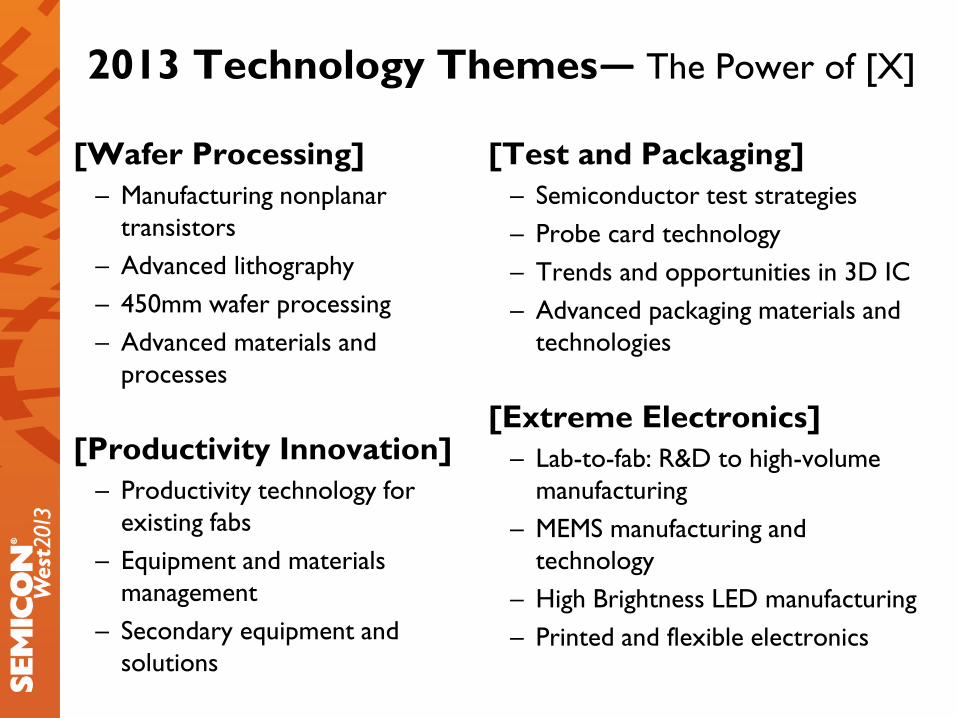
Intel – 450mm Robert E. Bruck, corporate vice president and general manager of Technology Manufacturing Engineering (TME), Intel Corporation, and Intel 450mm Equipment Program Manager Mario Abravanel make the first public presentation of a fully patterned 450mm silicon wafer at the SEMI Industry Strategy Symposium (ISS) on January 15, 2013. Bruck said the wafer was patterned with 26nm features using nano imprint lithography and that thousands of similar wafers will be made available in the coming quarters to suppliers engaged in 450mm tool development.
Intel presents fully patterned 450mm silicon wafer @ ISS 2013
Source: SEMI ISS2013 & “Highlights” @ www.semi.org

At ISS 2013 - Intel Receives the SEMI Award for a Process and Technology Integration Breakthrough — the High-k Solution
The Team Mark Bohr, senior fellow and director of Process Architecture and Integration, Logic Technology Development, Intel Robert Chau, senior fellow and director of Transistor Research and Nanotechnology, Components Research, Intel Suman Datta, professor, Electrical Engineering, Pennsylvania State University* Mark Doczy, senior engineer in Advanced Transistor and Nanotechnology Group, Components Research, Intel Brian Doyle, principal engineer in Advanced Transistor and Nanotechnology Group, Components Research, Intel Tahir Ghani, fellow and director of Transistor Technology and Integration, Logic Technology Development, Intel Jack Kavalieros, principal engineer in Advanced Transistor and Nanotechnology Group, Components Research, Intel Matthew Metz, senior engineer in Advanced Transistor and Nanotechnology Group, Components Research, Intel Kaizad Mistry, vice president and director of Logic Technology Integration, Logic Technology Development, Intel
The Intel team was honored for their contribution to the first development, integration and introduction of a successful high-k dielectric and metal electrode gate stack for CMOS IC production, first implemented at the 45nm node in 2007.

Opening KeynoteTransforming the Semiconductor Industry to Meet the Demands of a New EraAjit Manocha, CEO Global Foundries
Session 1: Economic and Market TrendsSession Keynote: Dr. John C. WilliamsPresident and CEO, Federal Reserve Bank of San Francisco
"Heavy Lifting"- A Global Economic Overview for 2013Bruce Kasmank Chief Economist and Managing Director of Global Research, JP Morgan
Geopolitical Outlook 2013: Crises of Leadership and Balances of PowerMatthew Gertken, University of Texas at Austin
The “New” IC Industry Cycle ModelBill McClean, IC Insights
Session 2: Semiconductor Markets Session Keynote: Semiconductor Markets in 2020: Perils and OpportunitiesAndy Oberst, Senior VP, Strategy & Corporate Development, Qualcomm
Semiconductor Demand Mapped on the Compute, Communication and Storage ContinuumSatya Kumark, Director, Credit Suisse
Intel - Michael BellVice President, General Manager, Mobile and Communications Group, Intel Corporation
It's Now a Mobile World: So What's Next?Simon Segars, President, ARM
IMFT Joint Venture and the Evolution of Flash MemoryKeyvan Esfarjani, Intel Vice President, Technology & Manufacturing Group, Co-CEO, IM Flash Technologies
Agenda – Day 1

Highlights • Ajit discussed the dynamic technology and economic needs of mobile computing that is
driving new approaches to the chip design-to-production cycle. – Calling it “Foundry 2.0,” Ajit sees outsourced semiconductor manufacturing moving toward a more IDM-
like model, creating new collaboration models and techniques to close the gap between process teams at foundries and design teams at the fabless companies.
• Other Key points: – The Industry faces daunting technical challenges like 3D stacking, 450mm fabs, new transistor
architectures, multi-patterning, and the uncertainties to lithography-based scaling, product development paths with virtual teams will evolve and adapt rapidly in the coming months and years.
– With new fabs now costing upwards of $8 billion and leading-edge manufacturing investments expected to exceed $40 billion this year alone, global economic trends and forces — increasingly influenced by uncertain consumer spending in both developed and emerging markets — have never been more important to the semiconductor ecosystem.
Ajit Manocha, CEO of GLOBALFOUNDRIES Transforming the Semiconductor Industry to Meet the Demands of a New Era

Dr. John C. Williams, President and CEO of the Federal Reserve Bank of San Francisco (Full Presentation Text)
– “Many businesses are locked into a paralyzing state of anxiety.” – Williams used the ISS conference to lessen uncertainty and anxiety in the
capital markets, pledging to keep interest rates near zero until the unemployment rate drops to 6.5 percent, as long as inflation expectations do not climb above 2.5 percent.
Bruce Kasman, Chief Economist and Managing Director of Global Research, J.P. Morgan
– Bruce on the economic outlook. “A positive economic outlook, especially in the second half of the year, that is “bumpy, better and less risky.””
– Bruce sees Asia leading the economic rebound, as China demand accelerates with the change in leadership and improved access to credit.

Matthew Gertken, University of Texas Austin Churchill scholar • Discussed the simmering “Asian cold war” developing as territorial disputes with China
generate an emerging “containment policy” by many of China’s neighbors. Andy Oberst, senior VP, Strategy and Corporate Development at Qualcomm • Looked at what mobile phones would likely look like in 2020, but also pointed out how
disruptive changes — not incremental changes — have always driven the mobile phone market. Satya Kumar, vice president at Credit Suisse • Discussed how original equipment makers like phone and computer manufacturers have always
benefitted from the declining cost of transistors and pondered, “Could stopping Moore’s Law be a good thing?”
Michael Bell, vice president, general manager, Mobile and Communications Group at Intel • Brought the audience up to date on the company’s mobile strategy, offering confidence that
Intel’s portfolio of RF baseband technologies, leading-edge scaling performance, and supply chain excellence will ultimately deliver significant success.

Session 3: Supply ChainIntel - Robert BruckVice President, General Manager, Technology Manufacturing Engineering
TEL's Perspective on Supply ChainTetsuro Higashi, Chairman of the Board, Tokyo Electron Limited
Deep Supplier CollaborationDonald Esses, Vice President, Operations and Quality, Qualcomm
Samsung Semiconductor - Ana HunterVP of Foundry Services
The Emerging Consequences of Materials within the Electronics EcosystemWayne Mitchell, Vice President, General Manager, Electronics, Air Products
Supply Chain PanelModerator, G. Dan Hutcheson, VLSI Research Ana Hunter, Samsung Semiconductor Robert Bruck, Intel Donald Esses, Qualcomm Tetsuro Higashi, Tokyo Electron Wayne Mitchell, Air Products
Agenda – Day 2 (AM)

Agenda – Day 2 (PM)

Session 5: Opportunities at the EdgeSession Keynote: Cognitive Systems and the Emergence of a New Era of ComputingDario Gil, Director, Industry Solutions, IBM Research
Utility Scale Solar Power ProjectsPeter Carrato, Fellow, Bechtel Corporation
Innovation in Technology Saturated VehiclesKal Gyimesi, IBM Software Group, Industrial Sector Offering Leader, IBM
“I’d Like That with Chips Please”Andrew Thompson, Founder and CEO, Proteus Digital Health
Session 6: Streetviews PanelModerator: Klaus Rinnen, Managing VP, Gartner Joseph Dews, Partner, AGC Partners Jason Hutchinson, Managing Director, Head of the Technology Group, Houlihan Lokey Mahesh Sanganeria, Director, RBC Capital Markets Isaac Sudit, Vice President and Investment Analyst, The Capital Research Global Investors
Agenda – Day 3
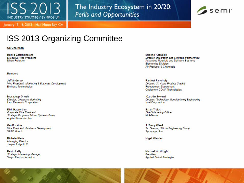
ISS 2013 Organizing Committee

Agenda
• SEMI Update • ISS 2013 - Highlights and Insights • SEMI Programs - Chapter Report • Member Spotlight – Applied Materials • Q&A • Closing Remarks

SEMI Americas Regional Programs
February, 2013
Lin Tso

SEMI Americas
40
Regional Chapters
Northeast
Chair- Jim Brown
Vice-Chair- Rob Nine
Arizona
Chair-April Rossrucker Vice-Chair- Lisa Neeley
Pacific Northwest
Chair-John Grimshaw
Vice-Chair- Rudy Kellner
Austin
Chair-Ken Parmerter
Vice-Chair- Greg Sajbel
The Regional Chapter’s goal is to identify, prioritize, and help solve challenges impacting SEMI members around the following key themes: • Workforce Development/Education • Technology and Innovation • Regional Stakeholder Outreach

Importance of Education/Workforce Development
• Workforce development is an important initiative for our SEMI
members. We must prepare the microelectronics workforce with a pipeline of skilled workers. At the same time, thought leaders must inspire tomorrow’s workforce to choose careers in our industry.
• That is the goal of the workforce development and education
activities and was the motivation towards creating a new “SEMI Professional Development Seminar” program

SEMI Professional Development Seminar
• The SEMI Pacific Northwest Chapter organized the SEMI Professional Development Workshop to connect College Students to semiconductor and related high technology industries.
• SEMI invited Industry Professionals with broad educational backgrounds and work experience to provide college students with real world perspective. Delivered valuable information in a face to face workshop. Helped students to choose their career direction and provided guidance in their particular field of interest.
• Provided college students with a look at career opportunities in the Semiconductor industry and to help excite college students about career opportunities in the high tech industries.
• The SEMI Pacific Northwest Chapter held the first seminar at Oregon State University last October, 2012.
• The SEMI Northeast Chapter held their first seminar at Northeastern University in February, 2013.

SEMI Professional Development Seminar • The Seminar covered: • Overview of careers in high tech, sought after degrees and
skill sets • First hand discussions with engineers, marketing and sales,
management, finance, recruiting and human resources. • The best approach to resumes and cover letters • Common Interview Questions and Answers • Preparing for the interview, tips on behavior, what to wear,
etc. • Learning and Networking with High Tech Industry Experts • Questions and Answers

Seminar Agenda 8:30am Introduction ~ Seminar Chairperson, FEI 8:35am Overview of SEMI ~ President of SEMI Americas, SEMI 8:45am Jobs in the Micro- and Nano-Electronics and High-Tech Semiconductor
Industry
9:45am Break 10:00am Strategies for Landing a Job in High Tech 10:40am The Interview Process: Telephone and Face-to-Face Interview Formats 11:40pm Breakout Sessions
– Day in the Life of a High Tech Engineer--Hear about the semiconductor industry from Applied Materials and Intel engineers
– Working on the Business Side--Using your technical skills for a career in sales, marketing and human resources
– Jump-start your career--Commandeering a successful job search – Is a career in High-Tech Startups, Business Operations, and General Management right for me?
Managing people and the bottom line

SEMI Professional Development Seminar Oregon State University, Oregon • Attendance, 45 undergrads, grad students and Ph.D. candidates from
Oregon State University (OSU), the University of Oregon, and the University of Washington
• Very well received, especially the talks delivered by industry experts
Northeastern University, Boston • Attendance, 35 Students • Instructors are all volunteers from High Tech Semiconductor Industries
such as Applied Materials, Entegris, Intel Corporation, TEL/NEXX Systems and others. They hold positions at these companies in Human Resources, Recruiting, Engineering, Marketing, Finance and Management, and Business Development.

SEMI SEMINAR AT OSU
Testimonials 1. Thank you for the opportunity to meet with Professional Leaders in the
semi-conductor industry. I learned a lot of valuable information and insight into the hiring process for these companies. I commend these wonderful, highly accomplished people for taking the time to offer their advice to those of us just starting out. I highly recommend continuing to organizing events like these. It was very inspirational, educational and a wonderful opportunity to meet with successful pioneers who have been in our shoes. If future events occur, I would definitely like to participate and attend. Again, thank you so much for making this event happen!
2. I was attending SEMI seminar on Friday. It was a great opportunity for students to know more about industry and get to talk with people from various positions in companies. I got inspired and learned a lot. Thanks for making this happen! Hope more events similar coming. Have a great day!

Call for Participation
Upcoming Professional Development Seminars will take place in the Fall of 2013…Opportunities for Industry Professional Volunteers, Sponsors, Venue Hosting, etc… If you are interested in participating…please contact Lin Tso, Email: [email protected] 408-943-7920

Agenda
• SEMI Update • ISS 2013 - Highlights and Insights • SEMI Programs - Chapter Report • Member Spotlight – Applied Materials • Q&A • Closing Remarks

Applied Materials – At A Glance
* As of November 14, 2012. Fiscal year-end October 28 ** Excluding temporary and interns

Professional Development Seminar • Our Challenge:
– Bring Educational Institutions and Industry Professionals together to enable pathway for student career success
• How did SEMI help? – SEMI Pacific Northwest Steering Committee – reinvigorated in Dec’11 – Charter formed with educational enhancement in mind, SEMI helped share learning from past
involvement to develop programs – Sub-team formed to drive development of Profession Development concept involving many
member companies – SEMI leadership helped kickoff first seminar with 45 students attending at Oregon State
University
• The Result: – Students received a full day of “real world” knowledge from Industry Leadership. – Students connecting with Companies for future career opportunities – Excellent for both the
Students and the Member Companies

Agenda
• SEMI Update • ISS 2013 - Highlights and Insights • SEMI Programs - Chapter Report • Member Spotlight – Applied Materials • Q&A • Closing Remarks

Agenda
• SEMI Update • ISS 2013 - Highlights and Insights • SEMI Programs - Chapter Report • Member Spotlight – Applied Materials • Q&A • Closing Remarks

Driving the Electronics Revolution
Thank You.