Embed Size (px)
Citation preview
Embedded Networking: Introduction – Serial/Parallel Communication
n telecommunication and computer science, serial communication is the process of sending data one bit at a time, sequentially, over a communication channel or computer bus. This is in contrast to parallel communication, where several bits are sent as a whole, on a link with several parallel channels.
Serial communication is used for all long-haul communication and most computer networks, where the cost of cable and synchronization difficulties make parallel communication impractical.
Many serial communication systems were originally designed to transfer data over relatively large distances through some sort of data cable.
The term "serial" most often refers to the RS232 port on the back of the original IBM PC, often called "the" serial port, and "the" serial cable designed to plug into it, and the many devices designed to be compatible with it.
Serial busesMany communication systems were generally originally designed to connect two integrated circuits on the same printed circuit board, connected by signal traces on that board (rather than external cables).
Integrated circuits are more expensive when they have more pins. To reduce the number of pins in a package, many ICs use a serial bus to transfer data when speed is not important. Some examples of such low-cost serial buses include SPI, I²C, UNI/O, and 1-Wire.
Serial versus parallelThe communication links across which computers—or parts of computers—talk to one another may be either serial or parallel. A parallel link transmits several streams of data simultaneously along multiple channels (e.g., wires, printed circuit tracks, or optical fibres); whereas, a serial link transmits only a single stream of data.
Although a serial link may seem inferior to a parallel one, since it can transmit less data per clock cycle, it is often the case that serial links can be clocked considerably faster than parallel links in order to achieve a higher data rate. A number of factors allow serial to be clocked at a higher rate:
Examples of serial communication architecturesI²C (Inter-Integrated Circuit), pronounced I-squared-C, is a multi-master, multi-slave, single-ended, serial computer bus invented by Philips Semiconductor (now NXP Semiconductors). It is typically used for attaching lower-speed peripheral ICs to processors and microcontrollers. Alternatively I²C is spelled I2C (pronounced I-two-C) or IIC (pronounced I-I-C).
Parallel communication
in computer science, parallel communication is a method of conveying multiple binary digits (bits) simultaneously. It contrasts with serial communication, which conveys only a single bit at a time; this distinction is one way of characterizing a communications link.
The basic difference between a parallel and a serial communication channel is the number of electrical conductors used at the physical layer to convey bits. Parallel communication implies more than one such conductor. For example, an 8-bit parallel channel will convey eight bits (or a byte) simultaneously, whereas a serial channel would convey those same bits sequentially, one at a time. If both channels operated at the same clock speed, the parallel channel would be eight times faster. A parallel channel may have additional conductors for other signals, such as a clock signal to pace the flow of data, a signal to control the direction of data flow, and handshaking signals.
Parallel communication is and always has been widely used within integrated circuits, in peripheral buses, and in memory devices such as RAM. Computer system buses, on the other hand, have evolved over time: parallel communication was commonly used in earlier system buses, whereas serial communications are prevalent in modern computers.
Examples of parallel communication systems IBM System/360 Direct Control Feature (1964).[1]:p.18 Standard System/360 had an eight-bit wide port. The process-control variant Model 44 had a
32-bit width.
Computer peripheral buses: ISA, ATA, SCSI, PCI and Front side bus, and the once-ubiquitous IEEE-1284 / Centronics "printer port"
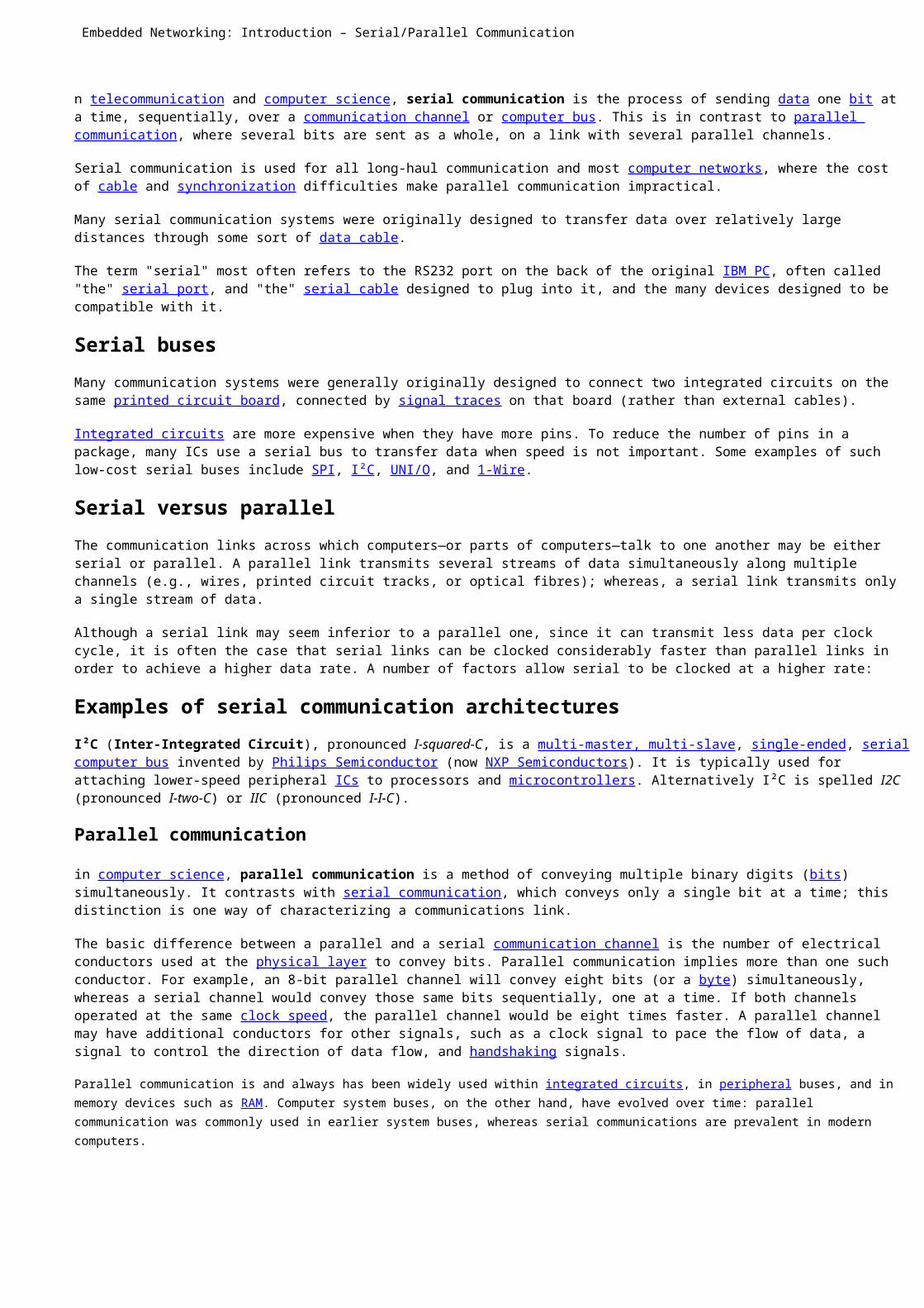
Serial and Parallel Communication Data can be transmitted between a sender and a receiver in two main ways: serial and parallel.
Serial communication is the method of transferring one bit at a time through a medium.
0 1 0 0 0 0 1 0
Parallel communication is the method of transferring blocks, eg: BYTEs, of data at the same time.
0 1 0 0 0 0 1 0
As you can appreciate parallel communication is faster than serial. For this reason, the internal connections in a computer, ie: the busses, are linked together to allow parallel communication. However, the use of parallel communication for longer distance data communication is unfeasible for economic and practical reasons, eg: amount of extra cable required and synchronisation difficulties. Therefore, all long distance data communications takes place over serial connections.
Three things should be considered when discussing serial communications and the equipment to carry this out:
Electrical standards associated with the interface Mechanical standards associated with the interface
Standards organisations involved
Serial communication protocols
Serial Communication Protocols
Serial communication protocols for data include the RS-232 protocol, which has been used for communication of modems. The MIDI protocol for music and sound applications is also a serial protocol.
The most common standard used for serial data transmission is called RS232C. It was set by the Electronics Industry Association and includes an assignment of the conductors in a 25-pin connector. It has also been used widely for data transfer over a modem.
MIDI Communication Protocol
Musical Instrument Digital Interface (MIDI) is a serial data transfer protocol. It uses one start bit, eight data bits and two stop bits and operates at 31.25 kilobaud. It uses two lines for input devices and three lines for output devices. The controlling device and the instrument controlled are electrically isolated from one another by the use of an opto-isolator and the avoidance of direct common grounds. The controlling device sends a signal through a UART to a 5-pin DIN "MIDI out" connector. On the input side, the signal drives the LED of an optoisolator, and the output of the optoisolator is sent to the UART of the receiving device for conversion to parallel information.
In controlling a device in an integrated music system, the status byte describes the action to be taken while the data bytes provide specific values or other instructions for the type of action requested.
UART
The conversion of parallel data inside a computer to serial data for use in serial communication is accomplished by a Universal Asynchronous Receiver/Transmitter (UART). UART chips are used for RS-232 and MIDI communication.
Serial Communication Protocols: CAN vs. SPITue, 2008-07-01 09:06 - webmaster
by Niall Murphy
Distributed systems require protocols for communication between microcontrollers. Controller Area Networks (CAN) and Serial Peripheral Interfaces (SPI) are two of the most common such protocols.
The beauty of using multiple processors in a single system is that the timing requirements of one processor can be divorced from the timing requirements of the other. In a real-time system, this quality can make the programming a lot easier and reduce the potential for race conditions. The price you pay is that you then have to get information from one processor to the other.
If you use one fast processor instead of two slow ones, passing information from one part of the software to another may be as simple as passing parameters to a function or storing the data in a global location. However, when the pieces of software that need to communicate are located on different processors, you have to figure out how to bundle the information into a packet and pass it across some sort of link. In this article, we'll look at two standard protocols, SPI and CAN, that can be used to communicate between processors, and also at some of the issues that arise in designing ad hoc protocols for small systems.
Building Protocols When I want two identical processors to communicate, I like to express messages as structs. For example, a setting message could be expressed as:
typedef enum { SPEED_SETTING, DIRECTION_SETTING, TIME_SETTING} SettingType;
typedef struct { SettingType type; int settingValue;} SettingMessage;
Such a structure can be passed byte by byte. As long as the same compiler with the same options is used on the sender and receiver, the enumerated type and int will be compatible (endianness). The number of bytes that must be transmitted is sizeof(SettingMessage).
If the processor architectures are different, this approach is not a good one. It's better to have a document that specifies the meaning of each byte, so byte ordering and size will always be explicit. This also means that more processing happens on both sides as bytes are combined to form larger types. It can get messy if a floating-point format has to be defined.
Another option is to define a text-based protocol. This is how most of the Internet works; HTTP and SMTP are both built on text protocols. This approach allows the protocol to remain architecture agnostic. Text is less efficient than a protocol where each byte is given a meaning, but the upside is a protocol that's easy for a human to read and debug.
Serial Peripheral Interface (SPI) Serial Peripheral Interface (SPI) is a clocked serial link. There are Rx and Tx lines, as in a standard serial link, and there is also a clock line. Clocking the data allows greater data transfer speeds. The clock is driven by one side of the interface, which is called the master. Each time the master drives a pulse on the clock line, one bit is transferred in each direction. The Tx line sends out a bit, while the Rx line receives a bit. While this means that the amount of data sent and the amount of data received must be equal, it's trivial to provide dummy data when you don't have anything interesting to send. In fact, SPI is common in applications where the data only goes in one direction and the opposite direction always passes a dummy value.
Since the master controls the clock, the master is in charge of flow control. If the master doesn't currently have time to process a byte of received data, the master can make sure that no data is received by not providing any clock pulses. This reduces the need for interrupts on the master and generally makes real-time management easier. However, there's a price to be paid on the slave side.
The frequency at which the slave transmits is controlled by the master. The slave must always have a valid byte ready to send, since it does not have any control over when the next clock pulse will appear, effectively requesting more data. If the slave device is dedicated to a single job, this may not be difficult. Consider a thermistor that communicates as an SPI slave. It could provide a single buffer of one byte that is always populated with the last temperature reading. Whenever clock pulses appear, that byte is transmitted and the master gets a reading.
In one project I worked on, we used SPI to communicate between two microcontrollers. In this case, some of the slave's responsibilities were quite troublesome. The microcontrollers were both PICs with built-in SPI controllers. Sequences of each 16 bytes were treated as a packet and included a checksum. While the master could communicate via polling, the slave needed to be interrupt-driven.
Bear in mind that as a single character is transmitted, so too is a single character received. The interrupt is generated at the end of each character. The slave needs to place the next character in the buffer before the master starts pulsing the clock line again. This gives the slave a window that may be very short. If you miss your deadline, the last character will be transmitted again, and, at the end of the 16 byte packet, the checksum will fail. The master and slave are no longer synchronized, and some recovery must take place.
Getting the master to pause after each byte is transmitted would give the slave a longer window, but this tactic can compromise the master; it also doesn't solve the problem completely, since the slave still has a hard deadline. One of the great advantages of using multiple processors is that the real-time issues from one portion of the software can be handled independently of the real-time requirements of any other part. Ironically, in this case, we have a situation where the real-time performance of the slave depends on the timing characteristics of the master, so we've done our design a disservice.
Faced with these timing issues, one solution is to avoid using the SPI's ability to transmit and receive at the same time. We can provide an extra signal that the slave asserts when it wants to transmit. When the master sees this signal, it knows that the slave has a byte ready, and the master then provides the clock to fetch that byte. When the master has something to send, it checks that the slave is not sending before clocking out its own byte; anything simultaneously received from the slave is ignored. Taking it in turns like this means that a large fraction of the potential bandwidth is lost. In exchange, you get more reliable and flexible software.
The serial peripheral interface, as the name suggests, is good for dedicated peripherals with a simple job to do, but causes some frustration when used for general purpose communications between independent processors.
Controller Area Network (CAN)
Controller Area Network (CAN) is a multi-drop bus protocol, so it can support many communicating nodes. 1 The advantages are obvious. The disadvantage of moving to more than two nodes is that you now require some addressing mechanism to indicate who sent a message, and who should receive it. The CAN protocol is based on two signals shared by all nodes on the network. The CAN_High and CAN_Low signals provide a differential signal and allow collision detection. If both lines go high, two different nodes must be trying to drive two different signals, and one will then back off and allow the other to continue.
CAN is used in almost every automobile manufactured in Europe. In the U.S., CAN is popular in factory automation, where the DeviceNet protocol uses CAN as its lower layer.
The biggest difference between CAN and SPI is that the CAN protocol defines packets. In SPI (and serial interfaces in general), only the transmission of a byte is fully defined. Given a mechanism for byte transfer, software can provide a packet layer, but no standard size or type exists for a serial packet. Since packet transfer is standardized for CAN, it's usually implemented in hardware. Implementing packets, including checksums and backoff-and-retry mechanisms, in hardware hides a whole family of low-level design issues from the software engineer.
The program can place a packet in a CAN controller's buffer and not worry about interacting with the CAN hardware until the packet is sent or an entire packet has been received. The same level of control could be built into a serial controller, but unless it was standardized, that controller could only communicate with peers of the same type.
A CAN packet consists of an identifier that comprises either 11 bits or 29 bits and 8 bytes of data, along with a few other pieces of housekeeping like the checksum. The identifier is not defined by the CAN protocol, but higher level protocols can describe how the identifier can be divided into source, destination, priority, and type information. You could also define these bits yourself if you don't have to share the bus with devices outside of your control.
When controlling transmission byte by byte, you usually have to combine a number of bytes to say anything meaningful, except in cases as trivial as the thermistor example discussed earlier. However, in eight bytes you can express commands, report on parameter values, or pass calibration results.
For debugging purposes, communicating from a microcontroller to a PC is straightforward. By snooping the CAN bus from the PC, you can monitor the communications between the microcontrollers in the system, or you can imitate one side of the conversation by inserting test messages.
A product called USBcan from Kvaser provides an interface to the CAN bus through the PC's USB port. A number of other companies offer similar products, but what I found impressive about Kvaser was the quality of the software libraries available. The CANlib library provides an API for building and receiving CAN packets. The company also provides a version of the library compiled for my favorite PC development environment, Borland C++ Builder, which enabled me to build a nice GUI that showed all bus activity. The same program can be used for calibration, inserting text messages, and even downloading a new version of software to the device.
Each Kvaser product, whether ISA, PCI, PCMCIA or USB-based, has a driver. Once the driver is installed, the applications built using Kvaser's libraries will work directly with that device. So, if I develop on a PC with a PCI card, I can still deploy my test software to a field engineer with a laptop and a PCMCIA card. Since the application I was working on was automotive, it was ideal to be able to send someone into a vehicle with a laptop. One of my few gripes with the supplied software is that it only supports the mainstream versions of Windows. Linux drivers would have been welcome, but Kvaser does not support it. (Open source drivers are available for some of the Kvaser ISA boards at the Linux CAN Project homepage.) 2
One of the most useful drivers from Kvaser is a virtual driver that doesn't require a CAN hardware interface. This allows one PC application to communicate with other PC applications running CAN software without any CAN hardware. You can therefore develop and test a PC program to communicate over the CAN bus without requiring any CAN hardware, as long as you write another PC test program to listen to whatever the first program is saying. This is useful if there isn't enough hardware to provide a system to each developer or if the prototype target is not yet available.
What is a serial data bus?A shared channel that transmits data one bit after the other over a single wire or fiber; for example, Ethernet uses a serial bus architecture. The I/O bus from the CPU to the peripherals is a parallel bus (16, 32 or 64 wires, etc.).
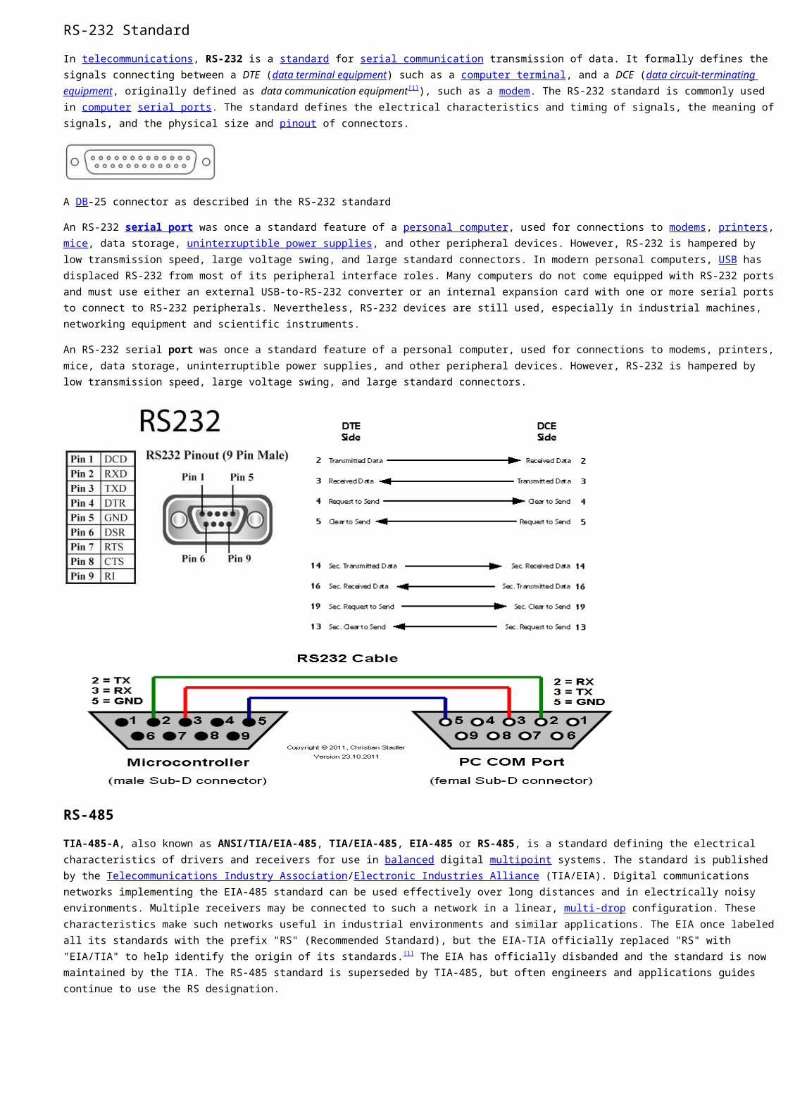
RS-232 Standard
In telecommunications, RS-232 is a standard for serial communication transmission of data. It formally defines the signals connecting between a DTE (data terminal equipment) such as a computer terminal, and a DCE (data circuit-terminating equipment, originally defined as data communication equipment[1]), such as a modem. The RS-232 standard is commonly used in computer serial ports. The standard defines the electrical characteristics and timing of signals, the meaning of signals, and the physical size and pinout of connectors.
A DB-25 connector as described in the RS-232 standard
An RS-232 serial port was once a standard feature of a personal computer, used for connections to modems, printers, mice, data storage, uninterruptible power supplies, and other peripheral devices. However, RS-232 is hampered by low transmission speed, large voltage swing, and large standard connectors. In modern personal computers, USB has displaced RS-232 from most of its peripheral interface roles. Many computers do not come equipped with RS-232 ports and must use either an external USB-to-RS-232 converter or an internal expansion card with one or more serial ports to connect to RS-232 peripherals. Nevertheless, RS-232 devices are still used, especially in industrial machines, networking equipment and scientific instruments.
An RS-232 serial port was once a standard feature of a personal computer, used for connections to modems, printers, mice, data storage, uninterruptible power supplies, and other peripheral devices. However, RS-232 is hampered by low transmission speed, large voltage swing, and large standard connectors.
RS-485
TIA-485-A, also known as ANSI/TIA/EIA-485, TIA/EIA-485, EIA-485 or RS-485, is a standard defining the electrical characteristics of drivers and receivers for use in balanced digital multipoint systems. The standard is published by the Telecommunications Industry Association/Electronic Industries Alliance (TIA/EIA). Digital communications networks implementing the EIA-485 standard can be used effectively over long distances and in electrically noisy environments. Multiple receivers may be connected to such a network in a linear, multi-drop configuration. These characteristics make such networks useful in industrial environments and similar applications. The EIA once labeled all its standards with the prefix "RS" (Recommended Standard), but the EIA-TIA officially replaced "RS" with "EIA/TIA" to help identify the origin of its standards.[1] The EIA has officially disbanded and the standard is now maintained by the TIA. The RS-485 standard is superseded by TIA-485, but often engineers and applications guides continue to use the RS designation.
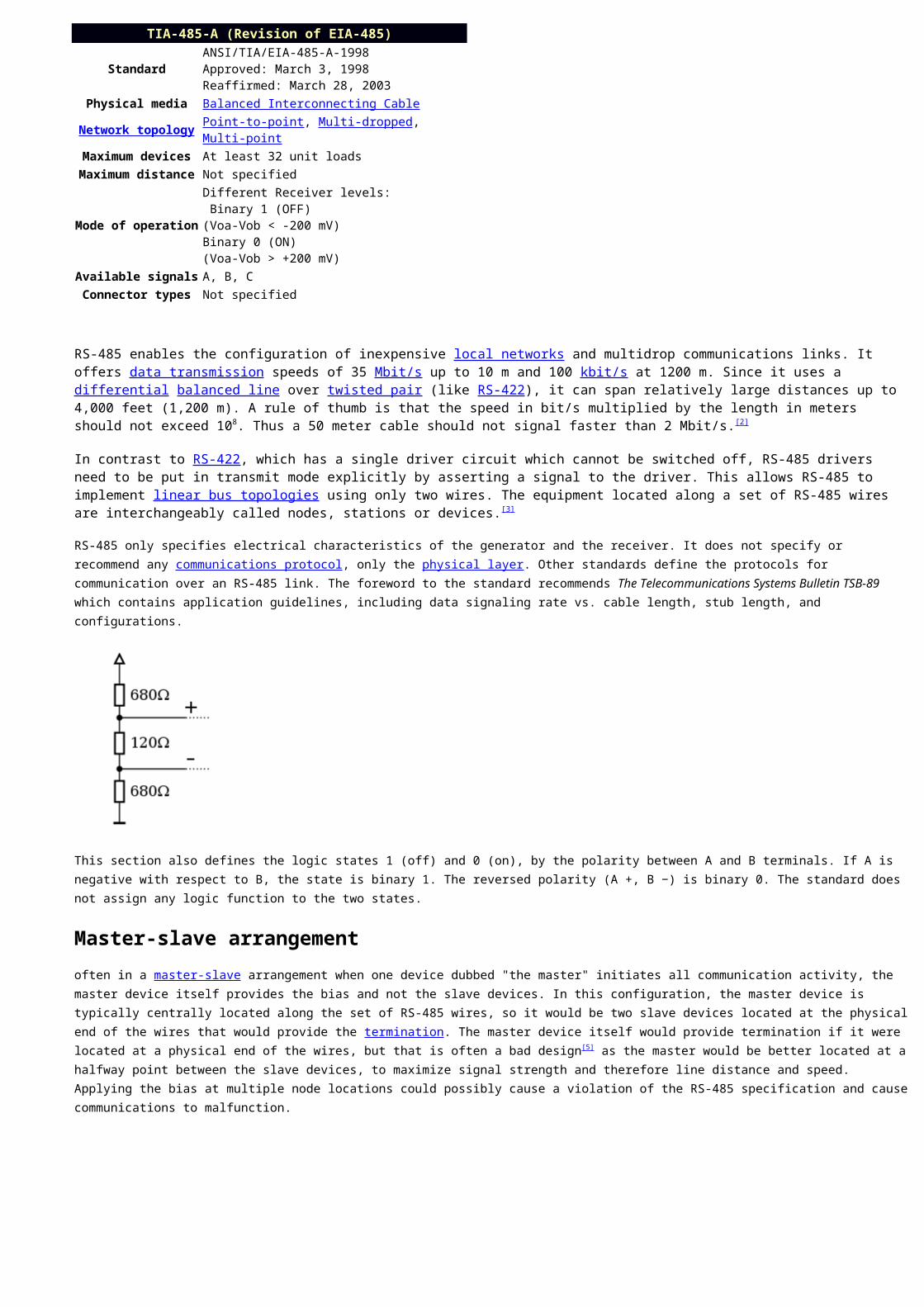
TIA-485-A (Revision of EIA-485)
StandardANSI/TIA/EIA-485-A-1998Approved: March 3, 1998Reaffirmed: March 28, 2003
Physical media Balanced Interconnecting CableNetwork topology Point-to-point, Multi-dropped, Multi-pointMaximum devices At least 32 unit loadsMaximum distance Not specified
Mode of operation
Different Receiver levels: Binary 1 (OFF)(Voa-Vob < -200 mV)Binary 0 (ON)(Voa-Vob > +200 mV)
Available signals A, B, CConnector types Not specified
RS-485 enables the configuration of inexpensive local networks and multidrop communications links. It offers data transmission speeds of 35 Mbit/s up to 10 m and 100 kbit/s at 1200 m. Since it uses a differential balanced line over twisted pair (like RS-422), it can span relatively large distances up to 4,000 feet (1,200 m). A rule of thumb is that the speed in bit/s multiplied by the length in meters should not exceed 108. Thus a 50 meter cable should not signal faster than 2 Mbit/s.[2]
In contrast to RS-422, which has a single driver circuit which cannot be switched off, RS-485 drivers need to be put in transmit mode explicitly by asserting a signal to the driver. This allows RS-485 to implement linear bus topologies using only two wires. The equipment located along a set of RS-485 wires are interchangeably called nodes, stations or devices.[3]
RS-485 only specifies electrical characteristics of the generator and the receiver. It does not specify or recommend any communications protocol, only the physical layer. Other standards define the protocols for communication over an RS-485 link. The foreword to the standard recommends The Telecommunications Systems Bulletin TSB-89 which contains application guidelines, including data signaling rate vs. cable length, stub length, and configurations.
This section also defines the logic states 1 (off) and 0 (on), by the polarity between A and B terminals. If A is negative with respect to B, the state is binary 1. The reversed polarity (A +, B −) is binary 0. The standard does not assign any logic function to the two states.
Master-slave arrangementoften in a master-slave arrangement when one device dubbed "the master" initiates all communication activity, the master device itself provides the bias and not the slave devices. In this configuration, the master device is typically centrally located along the set of RS-485 wires, so it would be two slave devices located at the physical end of the wires that would provide the termination. The master device itself would provide termination if it were located at a physical end of the wires, but that is often a bad design[5] as the master would be better located at a halfway point between the slave devices, to maximize signal strength and therefore line distance and speed. Applying the bias at multiple node locations could possibly cause a violation of the RS-485 specification and cause communications to malfunction.
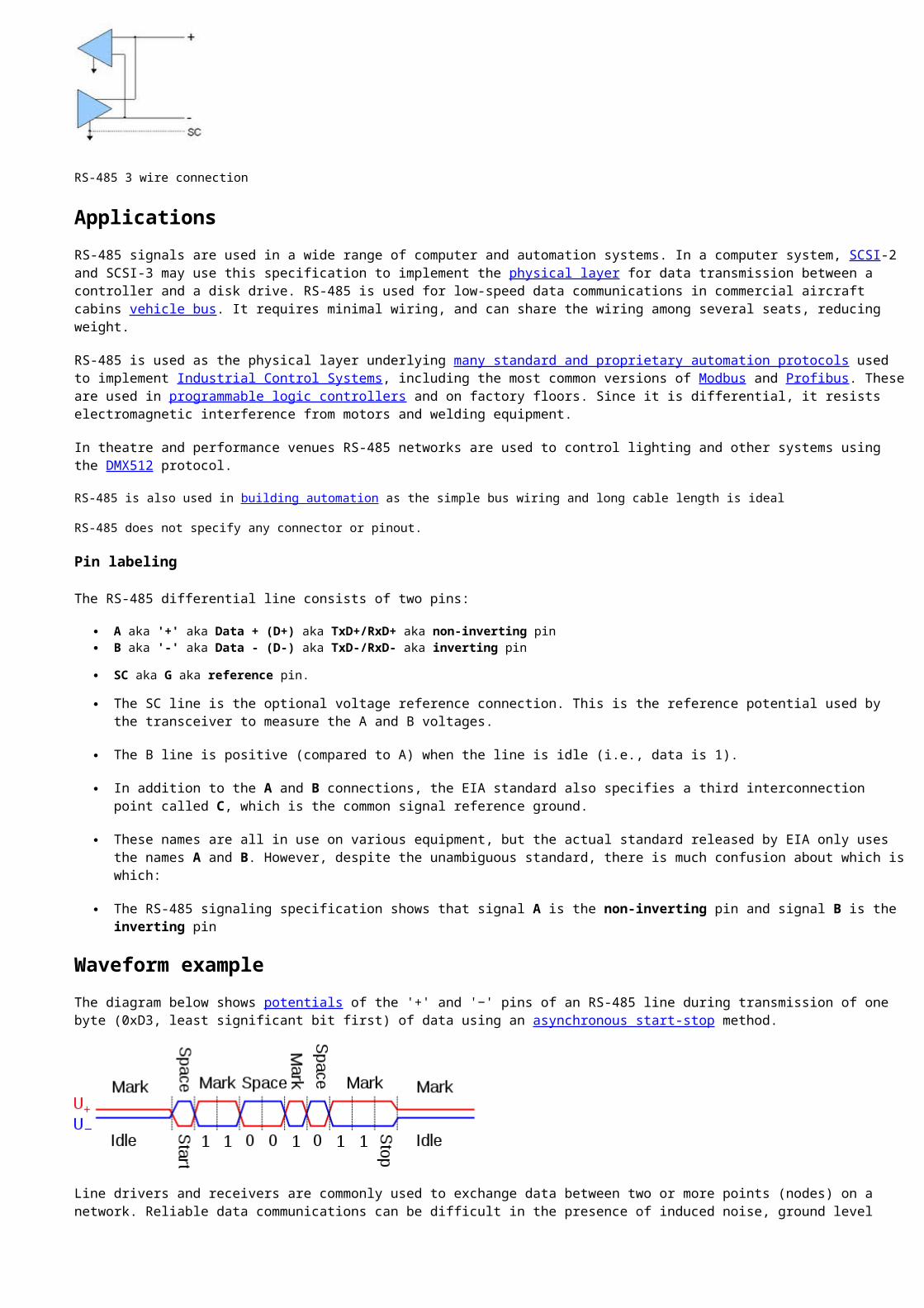
RS-485 3 wire connection
ApplicationsRS-485 signals are used in a wide range of computer and automation systems. In a computer system, SCSI-2 and SCSI-3 may use this specification to implement the physical layer for data transmission between a controller and a disk drive. RS-485 is used for low-speed data communications in commercial aircraft cabins vehicle bus. It requires minimal wiring, and can share the wiring among several seats, reducing weight.
RS-485 is used as the physical layer underlying many standard and proprietary automation protocols used to implement Industrial Control Systems, including the most common versions of Modbus and Profibus. These are used in programmable logic controllers and on factory floors. Since it is differential, it resists electromagnetic interference from motors and welding equipment.
In theatre and performance venues RS-485 networks are used to control lighting and other systems using the DMX512 protocol.
RS-485 is also used in building automation as the simple bus wiring and long cable length is ideal
RS-485 does not specify any connector or pinout.
Pin labeling
The RS-485 differential line consists of two pins:
A aka '+' aka Data + (D+) aka TxD+/RxD+ aka non-inverting pin B aka '-' aka Data - (D-) aka TxD-/RxD- aka inverting pin
SC aka G aka reference pin.
The SC line is the optional voltage reference connection. This is the reference potential used by the transceiver to measure the A and B voltages.
The B line is positive (compared to A) when the line is idle (i.e., data is 1).
In addition to the A and B connections, the EIA standard also specifies a third interconnection point called C, which is the common signal reference ground.
These names are all in use on various equipment, but the actual standard released by EIA only uses the names A and B. However, despite the unambiguous standard, there is much confusion about which is which:
The RS-485 signaling specification shows that signal A is the non-inverting pin and signal B is the inverting pin
Waveform exampleThe diagram below shows potentials of the '+' and '−' pins of an RS-485 line during transmission of one byte (0xD3, least significant bit first) of data using an asynchronous start-stop method.
Line drivers and receivers are commonly used to exchange data between two or more points (nodes) on a network. Reliable data communications can be difficult in the presence of induced noise, ground level differences, impedance mismatches, failure to effectively bias for idle line conditions, and other hazards associated with installation of a network.
The connection between two or more elements (drivers and receivers) should be considered a transmission line if the rise and/or fall time is less than half the time for the signal to travel from the transmitter to the receiver. Standards have been developed to insure compatibility between units provided by different manufacturers, and to allow for reasonable success in transferring data over specified distances and/or data rates. The Electronics Industry Association (EIA) has produced standards for RS485, RS422, RS232, and RS423 that deal with data communications. Suggestions are often made to deal with practical problems that might be encountered in a typical network. EIA standards where previously marked with the prefix "RS" to indicate recommended standard; however, the standards are now generally indicated as "EIA" standards to identify the standards organization. While the standards bring uniformity to data communications, many areas are not specifically covered and remain as "gray areas" for the user to discover (usually during installation) on his own.
Single-ended Data TransmissionElectronic data communications between elements will generally fall into two broad categories: single-ended and differential. RS232 (single-ended) was introduced in 1962, and despite rumors for its early demise, has remained widely used through the industry. The specification allows for data transmission from one transmitter to one receiver at relatively slow data rates (up to 20K bits/second) and short distances (up to 50Ft. @ the maximum data rate).
Independent channels are established for two-way (full-duplex) communications. The RS232 signals are represented by voltage levels with respect to a system common (power / logic ground). The "idle" state (MARK) has the signal level negative with respect to common, and the "active" state (SPACE) has the signal level positive with respect to common.
RS232 has numerous handshaking lines (primarily used with modems), and also specifies a communications protocol. In general if you are not connected to a modem the handshaking lines can present a lot of problems if not disabled in software or accounted for in the hardware (loop-back or pulled-up). RTS (Request to send) does have some utility in certain applications.
RS423 is another single ended specification with enhanced operation over RS232; however, it has not been widely used in the industry.
Differential Data TransmissionWhen communicating at high data rates, or over long distances in real world environments, single-ended methods are often inadequate. Differential data transmission (balanced differential signal) offers superior performance in most applications. Differential signals can help nullify the effects of ground shifts and induced noise signals that can appear as common mode voltages on a network.
RS422 (differential) was designed for greater distances and higher Baud rates than RS232. In its simplest form, a pair of converters from RS232 to RS422 (and back again) can be used to form an "RS232 extension cord." Data rates of up to 100K bits / second and distances up to 4000 Ft. can be accommodated with RS422. RS422 is also specified for multi-drop (party-line) applications where only one driver is connected to, and transmits on, a "bus" of up to 10 receivers.
While a multi-drop "type" application has many desirable advantages, RS422 devices cannot be used to construct a truly multi-point network. A true multi-point network consists of multiple drivers and receivers connected on a single bus, where any node can transmit or receive data.
"Quasi" multi-drop networks (4-wire) are often constructed using RS422 devices. These networks are often used in a half-duplex mode, where a single master in a system sends a command to one of several "slave" devices on a network. Typically one device (node) is addressed by the host computer and a response is received from that device. Systems of this type (4-wire, half-duplex) are often constructed to avoid "data collision" (bus contention) problems on a multi-drop network (more about solving this problem on a two-wire network in a moment).
RS485 meets the requirements for a truly multi-point communications network, and the standard specifies up to 32 drivers and 32 receivers on a single (2-wire) bus. With the introduction of "automatic" repeaters and high-impedance drivers / receivers this "limitation" can be extended to hundreds (or even thousands) of nodes on a network. RS485 extends the common mode range for both drivers and receivers in the "tri-state" mode and with power off. Also, RS485 drivers are able to withstand "data collisions" (bus contention) problems and bus fault conditions.
To solve the "data collision" problem often present in multi-drop networks hardware units (converters, repeaters, micro-processor controls) can be constructed to remain in a receive mode until they are ready to transmit data. Single master systems (many other communications schemes are available) offer a straight forward and simple means of avoiding "data collisions" in a typical 2-wire, half-duplex, multi-drop system. The master initiates a communications request to a "slave node" by addressing that unit. The hardware detects the start-bit of the transmission and automatically enables (on the fly) the RS485 transmitter. Once a character is sent the hardware reverts back into a receive mode in about 1-2 microseconds (at least with R.E. Smith converters, repeaters, and remote I/O boards).
Any number of characters can be sent, and the transmitter will automatically re-trigger with each new character (or in many cases a "bit-oriented" timing scheme is used in conjunction with network biasing for fully automatic operation, including any Baud rate and/or any communications specification, eg. 9600,N,8,1). Once a "slave" unit is addressed it is able to respond immediately because of the fast transmitter turn-off time of the automatic device. It is NOT necessary to introduce long delays in a network to avoid "data collisions." Because delays are NOT required, networks can be constructed, that will utilize the data communications bandwidth with up to 100% through put.
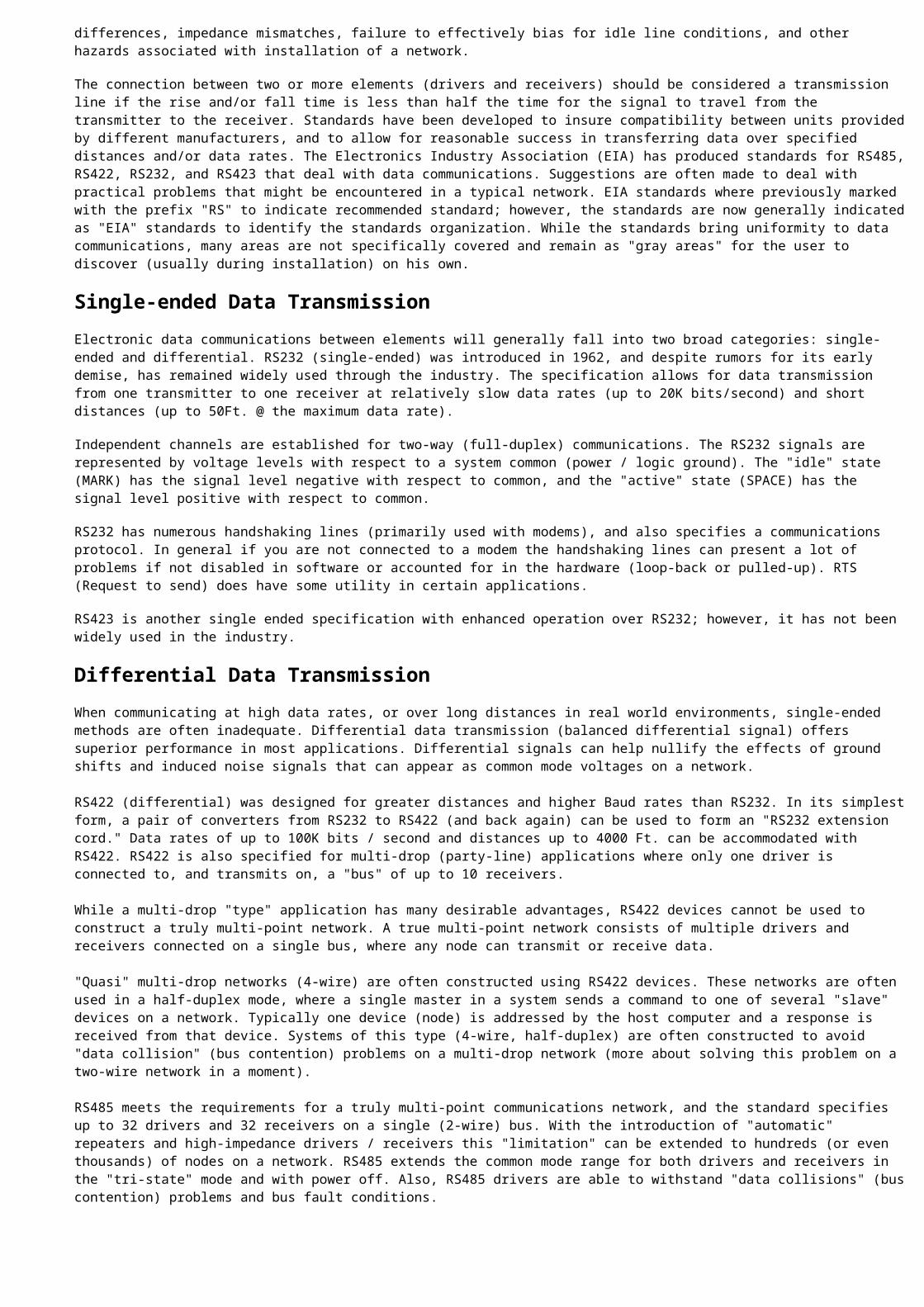
Below are the specifications for RS232, RS423, RS422, and RS485.
PECIFICATIONS RS232 RS423 RS422 RS485
Mode of Operation SINGLE-ENDED
SINGLE-ENDED DIFFERENTIAL DIFFERENTIAL
Total Number of Drivers and Receivers on One Line (One driver active at a time for RS485 networks)
1 DRIVER1 RECVR
1 DRIVER10 RECVR
1 DRIVER10 RECVR
32 DRIVER32 RECVR
Maximum Cable Length 50 FT. 4000 FT. 4000 FT. 4000 FT.Maximum Data Rate (40ft. - 4000ft. for RS422/RS485) 20kb/s 100kb/s 10Mb/s-100Kb/s 10Mb/s-100Kb/sMaximum Driver Output Voltage +/-25V +/-6V -0.25V to +6V -7V to +12V
Driver Output Signal Level (Loaded Min.) Loaded +/-5V to +/-15V +/-3.6V +/-2.0V +/-1.5V
Driver Output Signal Level (Unloaded Max) Unloaded +/-25V +/-6V +/-6V +/-6VDriver Load Impedance (Ohms) 3k to 7k >=450 100 54 Max. Driver Current in High Z State Power On N/A N/A N/A +/-100uA
Max. Driver Current in High Z State Power Off +/-6mA @ +/-2v +/-100uA +/-100uA +/-100uA
Slew Rate (Max.) 30V/uS Adjustable N/A N/AReceiver Input Voltage Range +/-15V +/-12V -10V to +10V -7V to +12VReceiver Input Sensitivity +/-3V +/-200mV +/-200mV +/-200mV Receiver Input Resistance (Ohms), (1 Standard Load for RS485) 3k to 7k 4k min. 4k min. >=12k
ular Products:
MHUBX8 IHV24AT DIFAR44 ICSX7HV ASC24T IRS422HV
.
http://www.rs485.com/pmhubx8.html website for more information
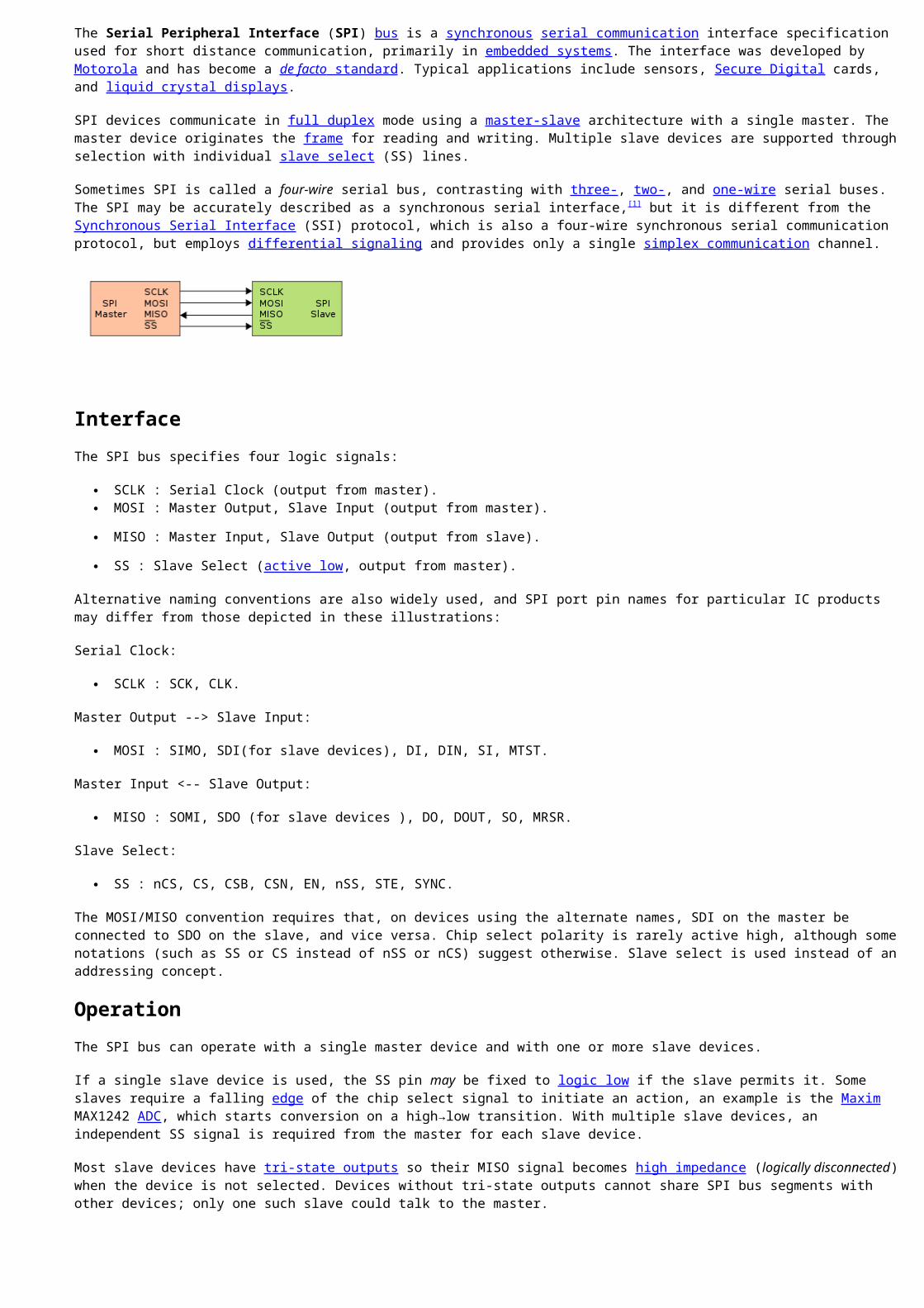
serial peripheral interface (SPI)The Serial Peripheral Interface (SPI) bus is a synchronous serial communication interface specification used for short distance communication, primarily in embedded systems. The interface was developed by Motorola and has become a de facto standard . Typical applications include sensors, Secure Digital cards, and liquid crystal displays.
SPI devices communicate in full duplex mode using a master-slave architecture with a single master. The master device originates the frame for reading and writing. Multiple slave devices are supported through selection with individual slave select (SS) lines.
Sometimes SPI is called a four-wire serial bus, contrasting with three-, two-, and one-wire serial buses. The SPI may be accurately described as a synchronous serial interface,[1] but it is different from the Synchronous Serial Interface (SSI) protocol, which is also a four-wire synchronous serial communication protocol, but employs differential signaling and provides only a single simplex communication channel.
InterfaceThe SPI bus specifies four logic signals:
SCLK : Serial Clock (output from master). MOSI : Master Output, Slave Input (output from master).
MISO : Master Input, Slave Output (output from slave).
SS : Slave Select (active low, output from master).
Alternative naming conventions are also widely used, and SPI port pin names for particular IC products may differ from those depicted in these illustrations:
Serial Clock:
SCLK : SCK, CLK.
Master Output --> Slave Input:
MOSI : SIMO, SDI(for slave devices), DI, DIN, SI, MTST.
Master Input <-- Slave Output:
MISO : SOMI, SDO (for slave devices ), DO, DOUT, SO, MRSR.
Slave Select:
SS : nCS, CS, CSB, CSN, EN, nSS, STE, SYNC.
The MOSI/MISO convention requires that, on devices using the alternate names, SDI on the master be connected to SDO on the slave, and vice versa. Chip select polarity is rarely active high, although some notations (such as SS or CS instead of nSS or nCS) suggest otherwise. Slave select is used instead of an addressing concept.
OperationThe SPI bus can operate with a single master device and with one or more slave devices.
If a single slave device is used, the SS pin may be fixed to logic low if the slave permits it. Some slaves require a falling edge of the chip select signal to initiate an action, an example is the Maxim MAX1242 ADC, which starts conversion on a high→low transition. With multiple slave devices, an independent SS signal is required from the master for each slave device.
Most slave devices have tri-state outputs so their MISO signal becomes high impedance (logically disconnected) when the device is not selected. Devices without tri-state outputs cannot share SPI bus segments with other devices; only one such slave could talk to the master.
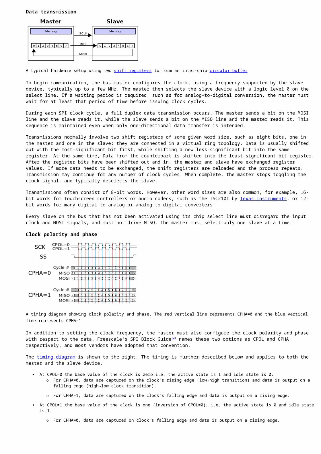
Data transmission
A typical hardware setup using two shift registers to form an inter-chip circular buffer
To begin communication, the bus master configures the clock, using a frequency supported by the slave device, typically up to a few MHz. The master then selects the slave device with a logic level 0 on the select line. If a waiting period is required, such as for analog-to-digital conversion, the master must wait for at least that period of time before issuing clock cycles.
During each SPI clock cycle, a full duplex data transmission occurs. The master sends a bit on the MOSI line and the slave reads it, while the slave sends a bit on the MISO line and the master reads it. This sequence is maintained even when only one-directional data transfer is intended.
Transmissions normally involve two shift registers of some given word size, such as eight bits, one in the master and one in the slave; they are connected in a virtual ring topology. Data is usually shifted out with the most-significant bit first, while shifting a new less-significant bit into the same register. At the same time, Data from the counterpart is shifted into the least-significant bit register. After the register bits have been shifted out and in, the master and slave have exchanged register values. If more data needs to be exchanged, the shift registers are reloaded and the process repeats. Transmission may continue for any number of clock cycles. When complete, the master stops toggling the clock signal, and typically deselects the slave.
Transmissions often consist of 8-bit words. However, other word sizes are also common, for example, 16-bit words for touchscreen controllers or audio codecs, such as the TSC2101 by Texas Instruments, or 12-bit words for many digital-to-analog or analog-to-digital converters.
Every slave on the bus that has not been activated using its chip select line must disregard the input clock and MOSI signals, and must not drive MISO. The master must select only one slave at a time.
Clock polarity and phase
A timing diagram showing clock polarity and phase. The red vertical line represents CPHA=0 and the blue vertical line represents CPHA=1
In addition to setting the clock frequency, the master must also configure the clock polarity and phase with respect to the data. Freescale's SPI Block Guide[2] names these two options as CPOL and CPHA respectively, and most vendors have adopted that convention.
The timing diagram is shown to the right. The timing is further described below and applies to both the master and the slave device.
At CPOL=0 the base value of the clock is zero,i.e. the active state is 1 and idle state is 0. o For CPHA=0, data are captured on the clock's rising edge (low→high transition) and data is output on a falling edge (high→low clock transition).
o For CPHA=1, data are captured on the clock's falling edge and data is output on a rising edge.
At CPOL=1 the base value of the clock is one (inversion of CPOL=0), i.e. the active state is 0 and idle state is 1.
o For CPHA=0, data are captured on clock's falling edge and data is output on a rising edge.
o For CPHA=1, data are captured on clock's rising edge and data is output on a falling edge.
That is, CPHA=0 means sampling on the first clock edge and , while CPHA=1 means sampling on the second clock edge, regardless of whether that clock edge is rising or falling. Note that with CPHA=0, the data must be stable for a half cycle before the first clock cycle.
In other words, CPHA=0 means transmitting data on the active to idle state and CPHA=1 means that data is transmitted on the idle to active state edge. Note that if transmission happens on a particular edge, then capturing will happen on the opposite edge(i.e. if transmission happens on falling, then reception happens on rising and vice versa). The MOSI and MISO signals are usually stable (at their reception points) for the half cycle until the next clock transition. SPI master and slave devices may well sample data at different points in that half cycle.
This adds more flexibility to the communication channel between the master and slave.
Mode numbers
The combinations of polarity and phases are often referred to as modes which are commonly numbered according to the following convention, with CPOL as the high order bit and CPHA as the low order bit:
For "Microchip PIC" / "ARM-based" microcontrollers (note that NCPHA is the inversion of CPHA):
SPI ModeClock Polarity(CPOL/CKP)
Clock Edge(CKE/NCPHA)
0 0 1
1 0 0
2 1 1
3 1 0
For PIC32MX : SPI mode configure CKP,CKE and SMP bits.Set SMP bit,and CKP,CKE two bits configured as above table.
For other microcontrollers:
Mode CPOL CPHA
0 0 0
1 0 1
2 1 0
3 1 1
Another commonly used notation represents the mode as a (CPOL, CPHA) tuple; e.g., the value '(0, 1)' would indicate CPOL=0 and CPHA=1.
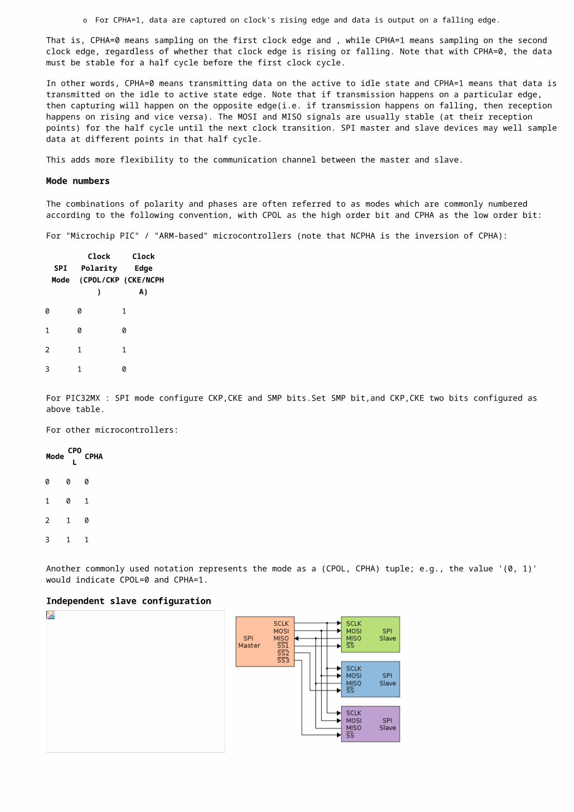
Independent slave configuration
Typical SPI bus: master and three independent slaves
In the independent slave configuration, there is an independent chip select line for each slave. A pull-up resistor between power source and chip select line is highly recommended for each independent device to reduce cross-talk between devices.[3] This is the way SPI is normally used. Since the MISO pins of the slaves are connected together, they are required to be tri-state pins (high, low or high-impedance).
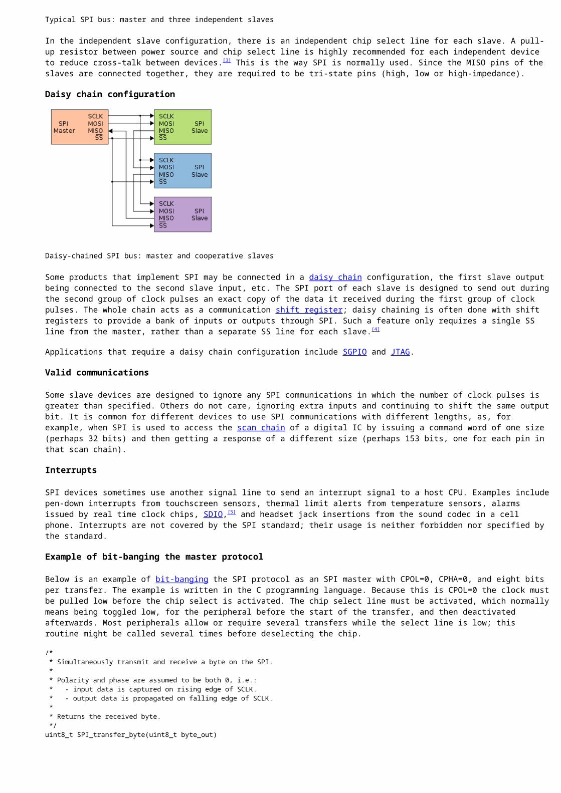
Daisy chain configuration
Daisy-chained SPI bus: master and cooperative slaves
Some products that implement SPI may be connected in a daisy chain configuration, the first slave output being connected to the second slave input, etc. The SPI port of each slave is designed to send out during the second group of clock pulses an exact copy of the data it received during the first group of clock pulses. The whole chain acts as a communication shift register; daisy chaining is often done with shift registers to provide a bank of inputs or outputs through SPI. Such a feature only requires a single SS line from the master, rather than a separate SS line for each slave.[4]
Applications that require a daisy chain configuration include SGPIO and JTAG.
Valid communications
Some slave devices are designed to ignore any SPI communications in which the number of clock pulses is greater than specified. Others do not care, ignoring extra inputs and continuing to shift the same output bit. It is common for different devices to use SPI communications with different lengths, as, for example, when SPI is used to access the scan chain of a digital IC by issuing a command word of one size (perhaps 32 bits) and then getting a response of a different size (perhaps 153 bits, one for each pin in that scan chain).
Interrupts
SPI devices sometimes use another signal line to send an interrupt signal to a host CPU. Examples include pen-down interrupts from touchscreen sensors, thermal limit alerts from temperature sensors, alarms issued by real time clock chips, SDIO,[5] and headset jack insertions from the sound codec in a cell phone. Interrupts are not covered by the SPI standard; their usage is neither forbidden nor specified by the standard.
Example of bit-banging the master protocol
Below is an example of bit-banging the SPI protocol as an SPI master with CPOL=0, CPHA=0, and eight bits per transfer. The example is written in the C programming language. Because this is CPOL=0 the clock must be pulled low before the chip select is activated. The chip select line must be activated, which normally means being toggled low, for the peripheral before the start of the transfer, and then deactivated afterwards. Most peripherals allow or require several transfers while the select line is low; this routine might be called several times before deselecting the chip.
/* * Simultaneously transmit and receive a byte on the SPI. * * Polarity and phase are assumed to be both 0, i.e.: * - input data is captured on rising edge of SCLK. * - output data is propagated on falling edge of SCLK. * * Returns the received byte. */uint8_t SPI_transfer_byte(uint8_t byte_out){ uint8_t byte_in = 0; uint8_t bit;
for (bit = 0x80; bit; bit >>= 1) { /* Shift-out a bit to the MOSI line */ write_MOSI((byte_out & bit) ? HIGH : LOW);
/* Delay for at least the peer's setup time */ delay(SPI_SCLK_LOW_TIME);
/* Pull the clock line high */ write_SCLK(HIGH);
/* Shift-in a bit from the MISO line */ if (read_MISO() == HIGH) byte_in |= bit;
/* Delay for at least the peer's hold time */ delay(SPI_SCLK_HIGH_TIME);
/* Pull the clock line low */ write_SCLK(LOW);
}
return byte_in;}
Intern integrated circuits (isquare c)I²C (Inter-Integrated Circuit), pronounced I-squared-C, is a multi-master, multi-slave, single-ended, serial computer bus invented by Philips Semiconductor (now NXP Semiconductors). It is typically used for attaching lower-speed peripheral ICs to processors and microcontrollers. Alternatively I²C is spelled I2C (pronounced I-two-C) or IIC (pronounced I-I-C).
Since October 10, 2006, no licensing fees are required to implement the I²C protocol. However, fees are still required to obtain I²C slave addresses allocated by NXP.[1]
Several competitors, such as Siemens AG (later Infineon Technologies AG, now Intel mobile communications), NEC, Texas Instruments, STMicroelectronics (formerly SGS-Thomson), Motorola (later Freescale), and Intersil, have introduced compatible I²C products to the market since the mid-1990s.
SMBus, defined by Intel in 1995, is a subset of I²C that defines the protocols more strictly. One purpose of SMBus is to promote robustness and interoperability. Accordingly, modern I²C systems incorporate policies and rules from SMBus, sometimes supporting both I²C and SMBus, requiring only minimal reconfiguration.
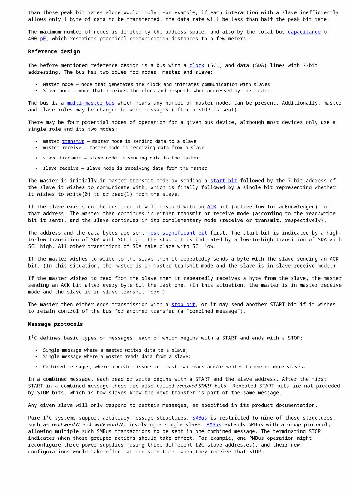
Design
A sample schematic with one master (a microcontroller), three slave nodes (an ADC, a DAC, and a microcontroller), and pull-up resistors Rp
I²C uses only two bidirectional open-drain lines, Serial Data Line (SDA) and Serial Clock Line (SCL), pulled up with resistors. Typical voltages used are +5 V or +3.3 V although systems with other voltages are permitted.
The I²C reference design has a 7-bit or a 10-bit (depending on the device used) address space.[3] Common I²C bus speeds are the 100 kbit/s standard mode and the 10 kbit/s low-speed mode, but arbitrarily low clock frequencies are also allowed. Recent revisions of I²C can host more nodes and run at faster speeds (400 kbit/s Fast mode, 1 Mbit/s Fast mode plus or Fm+, and 3.4 Mbit/s High Speed mode). These speeds are more widely used on embedded systems than on PCs. There are also other features, such as 16-bit addressing.
Note the bit rates are quoted for the transactions between master and slave without clock stretching or other hardware overhead. Protocol overheads include a slave address and perhaps a register address within the slave device as well as per-byte ACK/NACK bits. Thus the actual transfer rate of user data is lower than those peak bit rates alone would imply. For example, if each interaction with a slave inefficiently allows only 1 byte of data to be transferred, the data rate will be less than half the peak bit rate.
The maximum number of nodes is limited by the address space, and also by the total bus capacitance of 400 pF, which restricts practical communication distances to a few meters.
Reference design
The before mentioned reference design is a bus with a clock (SCL) and data (SDA) lines with 7-bit addressing. The bus has two roles for nodes: master and slave:
Master node — node that generates the clock and initiates communication with slaves Slave node — node that receives the clock and responds when addressed by the master
The bus is a multi-master bus which means any number of master nodes can be present. Additionally, master and slave roles may be changed between messages (after a STOP is sent).
There may be four potential modes of operation for a given bus device, although most devices only use a single role and its two modes:
master transmit — master node is sending data to a slave master receive — master node is receiving data from a slave
slave transmit — slave node is sending data to the master
slave receive — slave node is receiving data from the master
The master is initially in master transmit mode by sending a start bit followed by the 7-bit address of the slave it wishes to communicate with, which is finally followed by a single bit representing whether it wishes to write(0) to or read(1) from the slave.
If the slave exists on the bus then it will respond with an ACK bit (active low for acknowledged) for that address. The master then continues in either transmit or receive mode (according to the read/write bit it sent), and the slave continues in its complementary mode (receive or transmit, respectively).
The address and the data bytes are sent most significant bit first. The start bit is indicated by a high-to-low transition of SDA with SCL high; the stop bit is indicated by a low-to-high transition of SDA with SCL high. All other transitions of SDA take place with SCL low.
If the master wishes to write to the slave then it repeatedly sends a byte with the slave sending an ACK bit. (In this situation, the master is in master transmit mode and the slave is in slave receive mode.)
If the master wishes to read from the slave then it repeatedly receives a byte from the slave, the master sending an ACK bit after every byte but the last one. (In this situation, the master is in master receive mode and the slave is in slave transmit mode.)
The master then either ends transmission with a stop bit, or it may send another START bit if it wishes to retain control of the bus for another transfer (a "combined message").
Message protocols
I²C defines basic types of messages, each of which begins with a START and ends with a STOP:
Single message where a master writes data to a slave; Single message where a master reads data from a slave;
Combined messages, where a master issues at least two reads and/or writes to one or more slaves.
In a combined message, each read or write begins with a START and the slave address. After the first START in a combined message these are also called repeated START bits. Repeated START bits are not preceded by STOP bits, which is how slaves know the next transfer is part of the same message.
Any given slave will only respond to certain messages, as specified in its product documentation.
Pure I²C systems support arbitrary message structures. SMBus is restricted to nine of those structures, such as read word N and write word N, involving a single slave. PMBus extends SMBus with a Group protocol, allowing multiple such SMBus transactions to be sent in one combined message. The terminating STOP indicates when those grouped actions should take effect. For example, one PMBus operation might reconfigure three power supplies (using three different I2C slave addresses), and their new configurations would take effect at the same time: when they receive that STOP.
With only a few exceptions, neither I²C nor SMBus define message semantics, such as the meaning of data bytes in messages. Message semantics are otherwise product-specific. Those exceptions include messages addressed to the I²C general call address (0x00) or to the SMBus Alert Response Address; and messages involved in the SMBus Address Resolution Protocol (ARP) for dynamic address allocation and management.
In practice, most slaves adopt request/response control models, where one or more bytes following a write command are treated as a command or address. Those bytes determine how subsequent written bytes are treated and/or how the slave responds on subsequent reads. Most SMBus operations involve single byte commands.
Messaging example: 24c32 EEPROM
One specific example is the 24c32 type EEPROM, which uses two request bytes that are called Address High and Address Low. (Accordingly, these EEPROMs are not usable by pure SMBus hosts, which only support single byte commands or addresses.) These bytes are used to address bytes within the 32 kbit (4 kB) supported by that EEPROM; the same two byte addressing is also used by larger EEPROMs, such as 24c512 ones storing 512 kbits (64 kB). Writing and reading data to these EEPROMs uses a simple protocol: the address is written, and then data is transferred until the end of the message. (That data transfer part of the protocol also makes trouble for SMBus, since the data bytes are not preceded by a count and more than 32 bytes can be transferred at once. I²C EEPROMs smaller than 32 kbits, such as 2 kbit 24c02 ones, are often used on SMBus with inefficient single byte data transfers.)
A single message writes to the EEPROM. After the START, the master sends the chip's bus address with the direction bit clear (write), then sends the two byte address of data within the EEPROM and then sends data bytes to be written starting at that address, followed by a STOP. When writing multiple bytes, all the bytes must be in the same 32 byte page. While it is busy saving those bytes to memory, the EEPROM will not respond to further I²C requests. (That is another incompatibility with SMBus: SMBus devices must always respond to their bus addresses.)
To read starting at a particular address in the EEPROM, a combined message is used. After a START, the master first writes that chip's bus address with the direction bit clear (write) and then the two bytes of EEPROM data address. It then sends a (repeated) START and the EEPROM's bus address with the direction bit set (read). The EEPROM will then respond with the data bytes beginning at the specified EEPROM data address -— a combined message, first a write then a read. The master issues an ACK after each read byte except the last byte, and then issues a STOP. The EEPROM increments the address after each data byte transferred; multi-byte reads can retrieve the entire contents of the EEPROM using one combined message.
Physical layer
At the physical layer, both SCL and SDA lines are of open-drain design, thus, pull-up resistors are needed. Pulling the line to ground is considered a logical zero while letting the line float is a logical one. This is used as a channel access method. High speed systems (and some others) also add a current source pull up, at least on SCL; this accommodates higher bus capacitance and enables faster rise times.
An important consequence of this is that multiple nodes may be driving the lines simultaneously. If any node is driving the line low, it will be low. Nodes that are trying to transmit a logical one (i.e. letting the line float high) can see this, and thereby know that another node is active at the same time.
When used on SCL, this is called clock stretching and gives slaves a flow control mechanism. When used on SDA, this is called arbitration and ensures there is only one transmitter at a time.
When idle, both lines are high. To start a transaction, SDA is pulled low while SCL remains high. Releasing SDA to float high again would be a stop marker, signaling the end of a bus transaction. Although legal, this is typically pointless immediately after a start, so the next step is to pull SCL low.
Except for the start and stop signals, the SDA line only changes while the clock is low; transmitting a data bit consists of pulsing the clock line high while holding the data line steady at the desired level.
While SCL is low, the transmitter (initially the master) sets SDA to the desired value and (after a small delay to let the value propagate) lets SCL float high. The master then waits for SCL to actually go high; this will be delayed by the finite rise-time of the SCL signal (the RC time constant of the pull-up resistor and the parasitic capacitance of the bus), and may be additionally delayed by a slave's clock stretching.
Once SCL is high, the master waits a minimum time (4 μs for standard speed I²C) to ensure the receiver has seen the bit, then pulls it low again. This completes transmission of one bit.
After every 8 data bits in one direction, an "acknowledge" bit is transmitted in the other direction. The transmitter and receiver switch roles for one bit and the erstwhile receiver transmits a single 0 bit (ACK) back. If the transmitter sees a 1 bit (NACK) instead, it learns that:
(If master transmitting to slave) The slave is unable to accept the data. No such slave, command not understood, or unable to accept any more data. (If slave transmitting to master) The master wishes the transfer to stop after this data byte.
During the acknowledgment, SCL is always controlled by the master.
After the acknowledge bit, the master may do one of three things:
Prepare to transfer another byte of data: the transmitter set SDA, and the master pulses SCL high. Send a "Stop": Set SDA low, let SCL go high, then let SDA go high. This releases the I²C bus.
Send a "Repeated start": Set SDA high, let SCL go high, and pull SDA low again. This starts a new I²C bus transaction without releasing the bus.
Clock stretching using SCL
One of the more significant features of the I²C protocol is clock stretching. An addressed slave device may hold the clock line (SCL) low after receiving (or sending) a byte, indicating that it is not yet ready to process more data. The master that is communicating with the slave may not finish the transmission of the current bit, but must wait until the clock line actually goes high. If the slave is clock stretching, the clock line will still be low (because the connections are open-drain). The same is true if a second, slower, master tries to drive the clock at the same time. (If there is more than one master, all but one of them will normally lose arbitration.)
The master must wait until it observes the clock line going high, and an additional minimum time (4 μs for standard 100 kbit/s I²C) before pulling the clock low again.
Although the master may also hold the SCL line low for as long as it desires, the term "clock stretching" is normally used only when slaves do it. Although in theory any clock pulse may be stretched, generally it is the intervals before or after the acknowledgment bit which are used. For example, if the slave is a microcontroller, its I²C interface could stretch the clock after each byte, until the software decides whether to send a positive acknowledgment or a NACK.
Clock stretching is the only time in I²C where the slave drives SCL. Many slaves do not need to clock stretch and thus treat SCL as strictly an input with no circuitry to drive it. Some masters, such as those found inside custom ASICs may not support clock stretching; often these devices will be labeled as a "two-wire interface" and not I²C.
To ensure a minimum bus throughput, SMBus places limits on how far clocks may be stretched. Hosts and slaves adhering to those limits cannot block access to the bus for more than a short time, which is not a guarantee made by pure I²C systems.
Arbitration using SDA
Every master monitors the bus for start and stop bits, and does not start a message while another master is keeping the bus busy. However, two masters may start transmission at about the same time; in this case, arbitration occurs. Slave transmit mode can also be arbitrated, when a master addresses multiple slaves, but this is less common. In contrast to protocols (such as Ethernet) that use random back-off delays before issuing a retry, I²C has a deterministic arbitration policy. Each transmitter checks the level of the data line (SDA) and compares it with the levels it expects; if they do not match, that transmitter has lost arbitration, and drops out of this protocol interaction.
If one transmitter sets SDA to 1 (not driving a signal) and a second transmitter sets it to 0 (pull to ground), the result is that the line is low. The first transmitter then observes that the level of the line is different from that expected, and concludes that another node is transmitting. The first node to notice such a difference is the one that loses arbitration: it stops driving SDA. If it's a master, it also stops driving SCL and waits for a STOP; then it may try to reissue its entire message. In the meantime, the other node has not noticed any difference between the expected and actual levels on SDA, and therefore continues transmission. It can do so without problems because so far the signal has been exactly as it expected; no other transmitter has disturbed its message.
If the two masters are sending a message to two different slaves, the one sending the lower slave address always "wins" arbitration in the address stage. Since the two masters may send messages to the same slave address—and addresses sometimes refer to multiple slaves—arbitration must continue into the data stages.
Arbitration occurs very rarely, but is necessary for proper multi-master support. As with clock-stretching, not all devices support arbitration. Those that do generally label themselves as supporting "multi-master" communication.
In the extremely rare case that two masters simultaneously send identical messages, both will regard the communication as successful, but the slave will only see one message. Slaves that can be accessed by multiple masters must have commands that are idempotent for this reason.
Arbitration in SMBus
While I²C only arbitrates between masters, SMBus uses arbitration in three additional contexts, where multiple slaves respond to the master, and one gets its message through.
Although conceptually a single-master bus, a slave device that supports the "host notify protocol" acts as a master to perform the notification. It seizes the bus and writes a 3-byte message to the reserved "SMBus Host" address (0x08), passing its address and two bytes of data. When two slaves try to notify the host at the same time, one of them will lose arbitration and need to retry.
An alternative slave notification system uses the separate SMBALERT# signal to request attention. In this case, the host performs a 1-byte read from the reserved "SMBus Alert Response Address" (0x0c), which is a kind of broadcast address. All alerting slaves respond with a data bytes containing their own address. When the slave successfully transmits its own address (winning arbitration against others) it stops raising that interrupt. In both this and the preceding case, arbitration ensures that one slave's message will be received, and the others will know they must retry.
SMBus also supports an "address resolution protocol", wherein devices return a 16-byte "universal device ID" (UDID). Multiple devices may respond; the one with the lowest UDID will win arbitration and be recognized.
Circuit interconnections
I²C is popular for interfacing peripheral circuits to prototyping systems, such as the Arduino and Raspberry Pi. I²C does not employ a standardized connector, however, and board designers have created various wiring schemes for I²C interconnections. To minimize the possible damage due to plugging 0.1-inch headers in backwards, some developers have suggested using alternating signal and power connections of the following wiring schemes: (GND, SCL, VCC, SDA) or (VCC, SDA, GND, SCL).[4]
Buffering and multiplexing
When there are many I²C devices in a system, there can be a need to include bus buffers or multiplexers to split large bus segments into smaller ones. This can be necessary to keep the capacitance of a bus segment below the allowable value or to allow multiple devices with the same address to be separated by a multiplexer. Many types of multiplexers and buffers exist and all must take into account the fact that I²C lines are specified to be bidirectional. Multiplexers can be implemented with analog switches which can tie one segment to another. Analog switches maintain the bidirectional nature of the lines but do not isolate the capacitance of one segment from another or provide buffering capability.
Buffers can be used to isolate capacitance on one segment from another and/or allow I²C to be sent over longer cables or traces. Buffers for bi-directional lines such as I²C must use one of several schemes for preventing latch-up. I²C is open-drain so buffers must drive a low on one side when they see a low on the other. One method for preventing latch-up is for a buffer to have carefully selected input and output levels such that the output level of its driver is higher than its input threshold, preventing it from triggering itself. For example, a buffer may have an input threshold of 0.4 V for detecting a low, but an output low level of 0.5 V. This method requires that all other devices on the bus have thresholds which are compatible and often means that multiple buffers implementing this scheme cannot be put in series with one another.
Alternatively, other types of buffers exist that implement current amplifiers, or keep track of the state (i.e. which side drove the bus low) to prevent latch-up. The state method typically means that an unintended pulse is created during a hand-off when one side is driving the bus low, then the other drives it low, then the first side releases (this is common during an I²C acknowledgement).
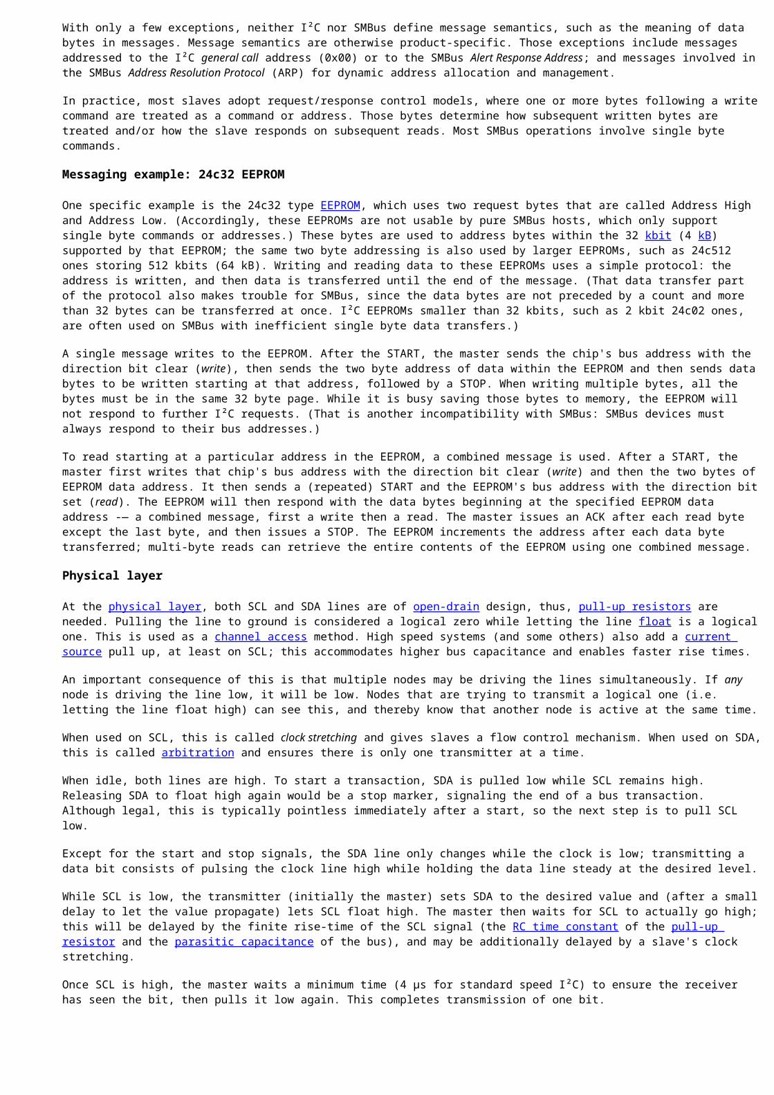
Timing diagram
1. Data Transfer is initiated with a START bit (S) signaled by SDA being pulled low while SCL stays high.2. SDA sets the 1st data bit level while keeping SCL low (during blue bar time.)
3. The data is sampled (received) when SCL rises (green) for the first bit (B1).
4. This process repeats, SDA transitioning while SCL is low, and the data being read while SCL is high (B2, Bn).
5. A STOP bit (P) is signaled when SDA is pulled high while SCL is high.
In order to avoid false marker detection, SDA is changed on the SCL falling edge and is sampled and captured on the rising edge of SCL.
Example of bit-banging the I²C Master protocol
Below is an example of bit-banging the I²C protocol as an I²C master. The example is written in pseudo C. It illustrates all of the I²C features described before (clock stretching, arbitration, start/stop bit, ack/nack)
// Hardware-specific support functions that MUST be customized:#define I2CSPEED 100void I2C_delay( void );bool read_SCL( void ); // Set SCL as input and return current level of line, 0 or 1bool read_SDA( void ); // Set SDA as input and return current level of line, 0 or 1void clear_SCL( void ); // Actively drive SCL signal lowvoid set_SDA( void ); // Actively drive SDA signal highvoid clear_SDA( void ); // Actively drive SDA signal lowvoid arbitration_lost( void );
bool started = false; // global data
void i2c_start_cond( void ) { if( started ) { // if started, do a restart cond // set SDA to 1 read_SDA(); I2C_delay();
while( read_SCL() == 0 ) { // Clock stretching // You should add timeout to this loop }
// Repeated start setup time, minimum 4.7us I2C_delay();
}
if( read_SDA() == 0 ) { arbitration_lost(); }
// SCL is high, set SDA from 1 to 0. clear_SDA(); I2C_delay(); clear_SCL(); started = true;
}
void i2c_stop_cond( void ){ // set SDA to 0 clear_SDA(); I2C_delay();
// Clock stretching while( read_SCL() == 0 ) { // add timeout to this loop. }
// Stop bit setup time, minimum 4us I2C_delay();
// SCL is high, set SDA from 0 to 1 set_SDA(); I2C_delay();
if( read_SDA() == 0 ) { arbitration_lost(); }
I2C_delay(); started = false;
}
// Write a bit to I2C busvoid i2c_write_bit( bool bit ) { if( bit ) { read_SDA(); } else { clear_SDA(); }
I2C_delay();
while( read_SCL() == 0 ) { // Clock stretching // You should add timeout to this loop }
// SCL is high, now data is valid // If SDA is high, check that nobody else is driving SDA if( bit && ( read_SDA() == 0 ) ) { arbitration_lost(); }
I2C_delay(); clear_SCL();
}
// Read a bit from I2C busbool i2c_read_bit( void ) { bool bit;
// Let the slave drive data read_SDA(); I2C_delay();
while( read_SCL() == 0 ) { // Clock stretching // You should add timeout to this loop }
// SCL is high, now data is valid bit = read_SDA(); I2C_delay(); clear_SCL();
return bit;
}
// Write a byte to I2C bus. Return 0 if ack by the slave.bool i2c_write_byte( bool send_start , bool send_stop , unsigned char byte ) {
unsigned bit; bool nack;
if( send_start ) { i2c_start_cond(); }
for( bit = 0; bit < 8; bit++ ) { i2c_write_bit( ( byte & 0x80 ) != 0 ); byte <<= 1; }
nack = i2c_read_bit();
if (send_stop) { i2c_stop_cond(); }
return nack;
}
// Read a byte from I2C busunsigned char i2c_read_byte( bool nack , bool send_stop ) { unsigned char byte = 0; unsigned char bit;
for( bit = 0; bit < 8; bit++ ) { byte = ( byte << 1 ) | i2c_read_bit(); }
i2c_write_bit( nack );
if( send_stop ) { i2c_stop_cond(); }
return byte;
}
void I2C_delay( void ) { volatile int v; int i;
for( i = 0; i < I2CSPEED / 2; i++ ) { v; }
}
Inter-Integrated Circuit (I2C)
As the name suggests, Inter-IC (or the Inter-Integrated Circuit), often shortened as I2C (pronounced eye-two-see), I2C (pronounced eye-squared-see), or IIC, was developed as a communication protocol to interact between different ICs on a motherboard, a simple internal bus system. It is a revolutionary technology developed by Philips Semiconductor (now NXP Semiconductors) in 1982, and is used to connect low speed peripherals (like keyboard, mouse, memory, IO/serial/parallel ports, etc.) to the motherboard (containing the CPU) operating at much higher speed.
These days you can find a lot of devices which are I2C compatible manufactured by a variety of companies (like Intel, TI, Freescale, STMicroelectronics, etc). Somewhere around the mid-1990s, Intel devised the SMBus protocol, a subset of I2C with strict protocols. Most modern day I2C devices support both, I2C and SMBus with little reconfiguration.
I2C Bus Interface
The most compelling thing about the I2C interface is that the devices are hooked up to the I2C bus with just two pins (and hence it is sometimes referred to as Two Wire Interface, or the TWI). Well of course, we do need two more pins for Vcc and ground, but that goes without saying.
I2C Bus Interface (Image source eeweb.com)
As you can see in the above diagram (taken from eeweb.com), all the devices are hooked up to the same I2C bus with just two pins. These devices could be the CPU, or IO devices, or ADC, or any other device which supports the I2C protocol. All the devices connected to the bus are classified as either being Master or Slave (just like SPI). We will discuss about it in a little while.
For now, let’s get to know more about the bus itself. The I2C bus consists of two bidirectional “open-drain” lines – SDA and SCL – pulled up with resistors as shown below.
I2C Bus Interface
Serial Data Line (SDA)
The Serial Data Line (SDA) is the data line (of course!). All the data transfer among the devices takes place through this line.
Serial Clock Line (SCL)
The Serial Clock Line (SCL) is the serial clock (obviously!). I2C is a synchronous protocol, and hence, SCL is used to synchronize all the devices and the data transfer together. We’ll learn how it works a little later in this post.
Open-Drain Lines
A little while ago (just above the previous image), I mentioned that SDA and SCL are open-drain (also called open-collector) lines pulled up with resistors. What does that mean? It means that the devices connected to the I2C bus are capable of pulling any of these two lines low, but they cannot drive them high. If any of the devices would ever want to drive the lines high, they would simply need to let go of that line, and it would be driven high by the pull up resistors (R1 and R2 in the previous image, or Rp in the next image).
For those who are interested, let’s have a closer look. Others, please skip this section and go to the next to next section (voltage levels and resistor values).
I2C Bus Interface – A Closer Look (Image source infoindustrielle.free.fr)
In the above image, you can clearly see the NMOS transistors inside the devices. In order for the device to pull any of the two lines low, it needs to provide a high voltage to the gate of the transistor (that’s how an NMOS transistor operates, right?). If the gate voltage is low, the NMOS transistor is not activated and the corresponding line is driven high.
I2C Data Validity
For the data to be valid on the SDA line, it must not change while the SCL is high. The data on the SDA line should change only and only when the SCL line goes low. If this standard is not followed, the data transfer becomes flawed, in which case it becomes a start/stop sequence (discussed later in this post). The following image illustrates the same.
I2C Data Validity (Image source infoindustrielle.free.fr)
Voltage Levels and Resistor Values
I2C supports a wide range of voltage levels, hence you can provide +5 volts, or +3.3 volts as Vcc easily, and other lower/higher voltages as well. This gives us a wide range of choices for the values of the pull-up resistors (R1 and R2). Anything within the range of 1k to 47k should be fine, however values lower than 10k are usually preferred.
Master and Slave
The concept of Master and Slave in I2C is quite similar to that of SPI. Just like SPI, all the devices are either Master or Slave. Master is the device which initiates the transfer and drives the clock line SCL. On a single I2C bus, there are usually multiple Slaves connected to a single Master.
However, just like SPI, we can also have multiple Masters connected to the same I2C bus. Since we want our lives to be a little simpler, we usually avoid such cases, but however I2C supports multi-bus master collision detection and arbitration for such cases (doesn’t make sense? Let’s forget about it for now!).
Speed
I2C supports serial 8-bit bi-directional data transfers up to a speed of 100 kbps, which is the standard clock speed of SCL. However, I2C can also operate at higher speeds – Fast Mode (400 kbps) and High Speed Mode (3.4 Mbps). Most of the devices are built to operate up to speeds of 100 kbps (remember that we discussed that I2C is used to connect low-speed devices?).
I2C Bus Transaction
Alright, now that we are familiar with the I2C bus interface, let’s look into how the data transfer actually takes place through that interface. I2C supports unidirectional as well as bidirectional data transfer as mentioned below. We will discuss about them in detail towards the end of the post.
Unidirectional Data Transfer o Master-transmitter to Slave-receiver (Case 1)
o Slave-transmitter to Master-receiver (Case 2)
Bidirectional Data Transfer
o Master to Slave and Slave to Master (Case 3)
Start/Stop SequenceIn order for the Master to start talking to the Slave(s), it must notify the Slave(s) about it. This is done using a special start sequence. Remember a little while ago we discussed about I2C data validity – that the SDA should not change while the SCL is high? Well, it doesn’t hold good for the start/stop sequence, which is why it makes them special sequences!
When the SCL is high and SDA goes from high to low (as shown in the following diagram), it marks the beginning of the transaction of Master with the Slave(s).
I2C Start Sequence
And when the SDA goes from low to high while the SCL is still high (as shown in the following diagram), it marks the end of the transaction of that Master with the Slave(s).
I2C Stop Sequence
NOTE: In between the start and stop sequences, the bus is busy and no other Master(s) (if any) should try to initiate a transfer.
Acknowledge SchemeAs mentioned earlier, I2C transfers 8 bits (1 byte) of data at a time. After the transfer of each byte is complete, the receiver must acknowledge it. To acknowledge, the receiver sends an ACK bit back to the transmitter. Here’s how it goes–
The transmitter (could be either Master or Slave) transmits 1 byte of data (MSB first) to the receiver during 8 clock pulses of SCL, after which it releases the SDA line i.e. the SDA line becomes HIGH for the ACK clock pulse.
The receiver (could be either Master or Slave, it depends) is obliged to generate an acknowledge after each byte sent by the transmitter by pulling the SDA line LOW for the ACK clock pulse (9th clock pulse) of SCL.
So overall, there are 9 SCL clock pulses required to transmit a byte of data. This is shown in the diagram below with the assumption that Master is the transmitter.
I2C Acknowledgement Scheme (Assumption: Master is the transmitter)Note: The legend shown at the bottom is only for SDA. SCL is always generated by the Master (whether transmitter or receiver).
So far so good. But what if the receiver does not (or could not) acknowledge the data sent to it? What happens then? Does the entire system break down?
Well, there are two cases to that situation.
Case 1: Slave is at the receiver’s end
Even in this case, there are two possible cases–
CASE 1A: The Slave-receiver does not acknowledge the Slave address (hey wait, what’s an address? We’ll get to it shortly). In that case, it simply leaves the SDA line HIGH. Now the Master-transmitter either generates a Stop sequence or attempts a repeated Start sequence.
CASE 1B: The Slave-receiver acknowledges the Slave address, but after some time it is unable to receive any data and leaves the SDA line HIGH during the ACK pulse. Even in this case, the Master-transmitter does the same – either generate a Stop sequence, or attempt a repeated Start sequence.
Case 2: Master is at the receiver’s end
Now this is a tricky situation. In this case, the Master is the one generating ACK, as well as responsible for generating Start/Stop sequence. Now how does that work out, especially when the transaction ends?
In this case, in order to signal the Slave-transmitter the end of data, the Master-receiver does NOT generate any ACK on the last byte clocked out of the Slave-transmitter. In this case, the Slave-transmitter must let go of the SDA line to allow Master to generate a Stop or a repeated Start sequence.
Makes sense? If it is confusing, hopefully it will make more sense when we actually program it for real.
I2C Device Addressing
Somewhere in the beginning of the tutorial, I mentioned that we can hook up a lot of devices to the I2C bus. But the Master can talk with only one of the Slaves at a time. Now how does that happen?
This is pretty similar to the situation inside a classroom. There is one teacher (Master) and a ridiculous number of students (Slaves). The teacher wants to ask a question to one of the students. How does she do that? Well, we do have a name, right? All the students have a unique name (address), and the teacher calls out the name first, right? Hey Max, could you explain why do we need casex statements in Verilog? Sounds familiar? Good old school days, eh? :D
Well, this is exactly what happens in case of I2C bus transaction. Every device hooked up to the bus has a unique address. As per the I2C specifications, this address is either 7 bits long, or 10 bits long. 10-bit addresses are rare, and since I am lazy, I am gonna skip it for now.
When we have 7-bit address, we can have up to a maximum of 27 = 128 devices hooked up to the I2C bus, with addresses 0 to 127. Now when the Master calls out to the Slave(s), it still needs to send out 8 bits of data. In this case, the Master appends an extra Read/Write (R/W’) bit to the 7 bits of address (note that W’ means Write complemented). Thus, the R/W’ bit is added to the LSB of the data byte. So now, the data sent looks somethings like this–
I2C Device AddressingNote: The legend shown at the bottom is only for SDA. SCL is always generated by the Master (whether transmitter or receiver).
Why should I bother about it?Well, this is a question which I expect all the newbies to ask. Unfortunately most of them don’t and then end up being frustrated. Why the heck is my I2C not working?!
Let’s take a scenario. You have an external EEPROM which you want to interface using I2C with your processor. You know that the address of the EEPROM is 0x50. You send this address to the bus expecting the EEPROM device to acknowledge. Does it acknowledge? Heck, NO!
So what’s the problem here? Yes, you guessed it right (hopefully). You forgot about the R/W’ bit! The address 0x50 is actually the 7-bit address (0b1010000).
Let’s make it right. Say you wanna perform page write operation on the EEPROM device. This means that you wish to write to the device and hence the R/W’ bit must be set to 0. Why you ask? Because the write is complemented. For read, R/W' = 1, whereas for write, R/W' = 0. Makes sense?
So what should be the correct (modified) address?
+ expand for answer
If you wanna perform sequential read operation on the same EEPROM device, what would be your (modified) address?
+ expand for answer
So, we can generalize that for write operations, the 8 bit address is even, whereas for read operations, the 8 bit address is odd.
I2C Data Transfer Protocol
Now that we are familiar with the I2C bus transactions and device addressing, let’s see how to transfer data using the I2C protocol and have a 10,000 foot view of the entire bus transaction.
Timing DiagramLet’s look at the timing diagram of an entire transaction – from start to stop!
Data Transfer Timing Diagram (Image source infoindustrielle.free.fr)
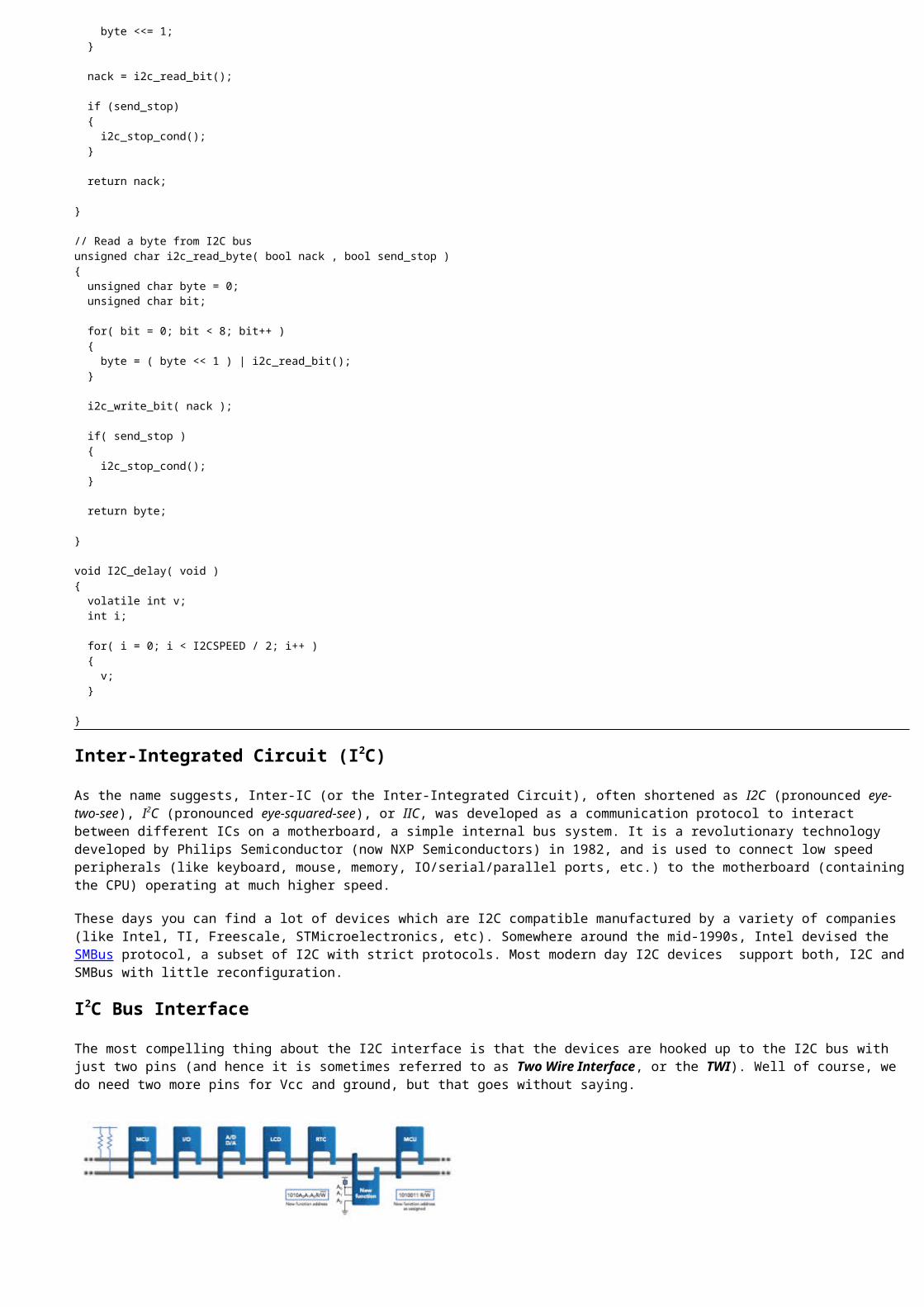
Let’s analyze it first. Before we begin, we all know what these slanted lines mean, right? The slanted lines are a representation of slew rate of the device/bus/system. Ideally, whenever a signal changes its state (from high to low or vice-versa), it is supposed to do so immediately. But in real scenario, it is almost impossible for it to happen without a time lag. The slanted lines refer to these time lags, also known as slew.
Alright, back to where we were.
The transaction starts with a START sequence. After the START sequence, the Master has to send the address of the Slave it wants to talk to. That’s the 7-bit ADDRESS (MSB first) followed by R/W’ bit
determining whether you want to read from the device or write into it.
The Slave responds by acknowledging the address. Yay! If it doesn’t send the ACK, we know what the Master does, right?
Once the Slave acknowledges the address, it means that it is now ready to send/receive data to/from the Master. Thus begins the data transfer. The DATA is always of 8 bits (MSB first), and the receiver has to send the ACK signal after each byte of data received.
When the transaction is over, the Master ends it by generating a STOP sequence. Alternatively, Master could also begin with a repeated START.
There are three possible cases of data transfer–
Case 1: Master-transmitter to Slave-receiver Case 2: Slave-transmitter to Master-receiver
Case 3: Bi-directional (R/W) in same data transfer
Case 1: Master (Transmitter) to Slave (Receiver) Data TransferLet’s have a look at the entire transaction first and then analyze it.
Master to Slave Data Transfer (Image source infoindustrielle.free.fr)
The Master sends the START sequence to begin the transaction. It is followed by Master sending 7-bit Slave address and the R/W’ bit set to zero. We set it to zero because the Master is writing to the Slave.
The Slave acknowledges by pulling the ACK bit low.
Once the Slave acknowledges the address, Master can now send data to the Slave byte-by-byte. The Slave has to send the ACK bit after every byte it receives.
This goes on till Slave can no longer receive data and does NOT send the ACK bit.
This is when the Master realizes that the Slave has gone crazy (not accepting anymore) and then STOPs the transaction (or reSTART).
We see that the data transfer never changes its direction. Data always flows from Master to Slave, which makes the setup quite easy.
An example of this case would be like performing page write operations on a EEPROM chip.
Case 2: Slave (Transmitter) to Master (Receiver) Data TransferLet’s look at the entire transaction again.
Slave to Master Data Transfer (Image source infoindustrielle.free.fr)
The Master sends the START sequence, followed by the 7-bit Slave address and the R/W’ bit set to 1. We set R/W’ bit to 1 because the Master is reading from the Slave.
The Slave acknowledges the address, thus ready to send data now.
Slave keeps on sending data to the Master, and the Master keeps on sending ACK to the Slave after each byte until it can no longer accept any more data.
When the Master feels like ending the transaction, it does not send the ACK, thus ending with the STOP sequence.
An example of this case could be an Analog to Digital Converter (ADC) sending data to the microcontroller continuously. The microcontroller accepts data as long as it wants to, after which it stops/finishes execution.
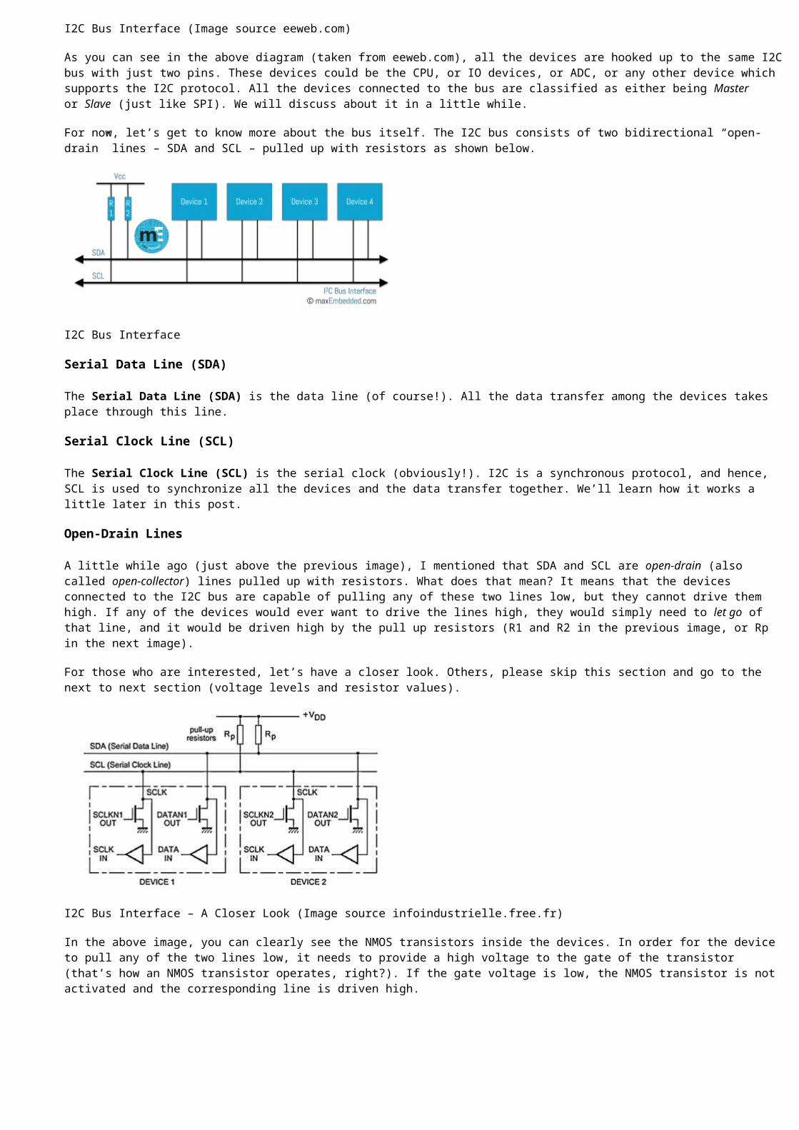
Case 3: Bi-directional Read and Write in same Data TransferOnce again, let’s look at the entire transaction first!
Bi-directional Data Transfer (Image source infoindustrielle.free.fr)
The Master sends out the START sequence, followed by the 7-bit Slave address and the R/W’ bit. The Slave acknowledges the address.
Depending upon the value of the R/W’ bit, read/write operations are performed (like the above two cases).
Whatever the case it may be, it always ends with the receiver not sending the ACK.
Until now, in the previous two cases, we have seen that the Master would close the connection. But in this case, the Master attempts a repeated START.
And the entire process repeats again, until the Master decides to STOP.
As we can see, a change of direction of data transfer might happen depending upon the R/W’ bits in the entire transaction.
An example of this case could be performing sequential read from a EEPROM chip. It is bi-directional because the CPU first writes the address from where it would like to start reading, followed by reading from the device. It is like, unless you tell the device from where you would like to start reading, how would it start sending you the data?
Clock Stretching
So far so good. Now let’s look at a very plausible complication. Suppose Master is reading data from the Slave. Everything goes on good as long as the Slave returns the data. What if… what if the Slave is not just ready yet? This is not an issue with devices like ADC or EEPROM, but with devices like a microcontroller. What if the Slave is a microcontroller, and the Master requests for a data which is not there in its cache. This would require the microcontroller to perform context switching, force it to search for it in the RAM, store it back in cache and then send it to the Master. This could (and definitiely would) take a much longer time than the clock pulses of the SCL, and everything would just go wrong!
Fortunately, there is a way, called Clock Stretching. The Slave is allowed to hold the clock line low until it is ready to give out the result. The Master must wait for the clock to go back to high before continuing with its work.
This is the only instance in the entire I2C protocol where the Slave is drives the clock line SCL. In many processors and microcontrollers, the low level hardware does this for us, so that we don’t have to worry about it while writing the code.
Why I2C?
Now that we are almost done with the basics of I2C communications, let’s take a moment to jot down some advantages of I2C.
I2C requires least number of pins (just two pins) to perform serial data transfer. The receiver always sends feedback to the transmitter (ACK) conveying a successful transmission, which leads to higher noise immunity as well.
Even though it has a slow standard speed of 100 kHz, modern I2C specifications support up to 3.4 MHz clock speed.
Summary I2C is an 8-bit bidirectional synchronous serial communication protocol requiring only two wires for operation. The I2C bus consists of two open-drain lines – SDA (data) and SCL (clock).
Several devices, being either Master or Slave, can be connected to the bus. The Master device must initiate the transfer and drive the clock line (SCL).
I2C supports the standard speed of 100 kbps, up to a maximum speed of 3.4 Mbps.
Master must generate unique Start and Stop conditions in order to mark the beginning and end of a transaction.
The receiver must send the ACK bit after every byte that it receives, failing which the Master may either Stop the transaction or attempt a repeated Start.
Every device connected to the I2C bus has either 7-bit or 10-bit address. An additional R/W’ bit is added to the address by the Master to determine whether it wants to read or write from/to the device.
Data transfer can be unidirectional (Master to Slave OR vice-versa) or bidirectional.
Slave can hold the clock line low until it is ready with the result to be sent to the Master, called Clock Stretching.
PC Parallel port programming
Parallel Port
A parallel port is a type of interface found on computers (personal and otherwise) for connecting peripherals. In computing, a parallel port is a parallel communication physical interface. It is also known as a printer port or Centronics port. It was an industry de facto standard for many years, and was finally
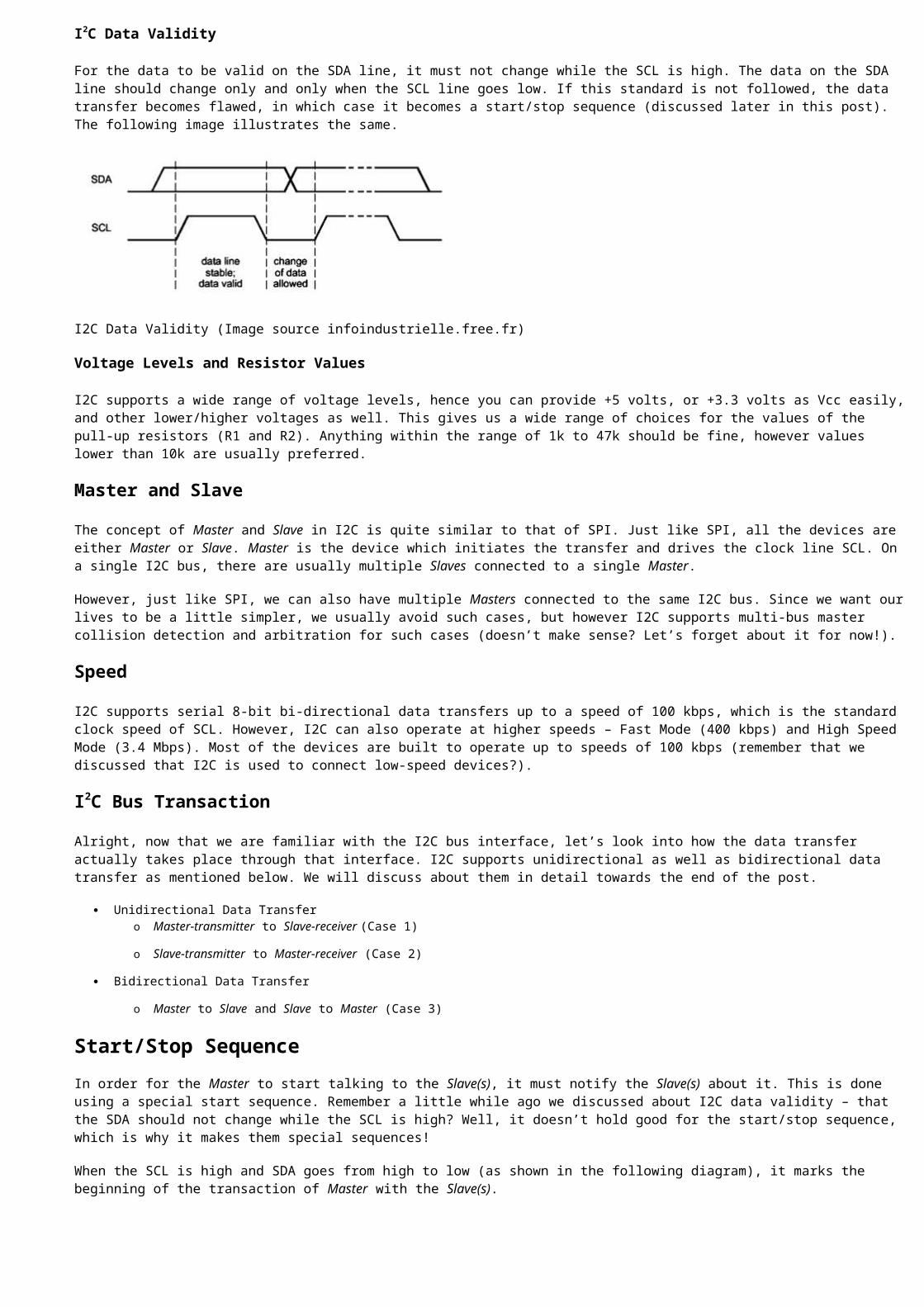
standardized as IEEE 1284 in the late 1990s, which defined the Enhanced Parallel Port (EPP) and Extended Capability Port (ECP) bi-directional versions. Today, the parallel port interface is seeing decreasing use because of the rise of Universal Serial Bus (USB) devices, along with network printing using Ethernet.
The parallel port interface was originally known as the Parallel Printer Adapter on IBM PC-compatible computers. It was primarily designed to operate a line printer that used IBM's 8-bit extended ASCII character set to print text, but could also be used to adapt other peripherals. Graphical printers, along with a host of other devices, have been designed to communicate with the system.
Pinouts for parallel port connectors.
Parallel Port Programming (PART 1): with CBy HarshaPerla
Parallel port is a very commonly known port, widely used to connect the printer to the PC. If you see
backside of your computer, there will be a port having 25 pins with a small symbol like this: . That port is known as LPT port or printer port. We can program this port for device control and data transfer. In this
article, we will learn basics of parallel port and programming the parallel port.
Parallel port basics:
In computers, ports are used mainly for two reasons: Device control and communication. We can program PC's Parallel ports for both. Parallel ports are mainly meant for connecting the printer to the PC. But we can program this port for many more applications beyond that.
Parallel ports are easy to program and faster compared to the serial ports. But main disadvantage is it needs more number of transmission lines. Because of this reason parallel ports are not used in long distance communications. Let us know the basic difference between working of parallel port and serial port. In serial ports, there will be two data lines: One transmission and one receive line. To send a data in serial port, it has to be sent one bit after another with some extra bits like start bit, stop bit and parity bit to detect errors. But in parallel port, all the 8 bits of a byte will be sent to the port at a time and a indication will be sent in another line. There will be some data lines, some control and some handshaking lines in parallel port. If three bytes of data 01000101 10011100 10110011 is to be sent to the port, following figures will explain how they are sent to the serial and parallel ports respectively. We can understand why parallel port
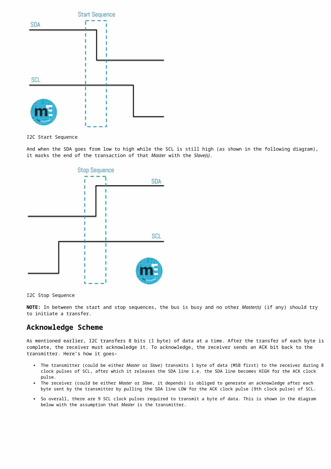
communication is faster compared to that of serial.
Parallel port basics:
In computers, ports are used mainly for two reasons: Device control and communication. We can program PC's Parallel ports for both. Parallel ports are mainly meant for connecting the printer to the PC. But we can program this port for many more applications beyond that.
Parallel ports are easy to program and faster compared to the serial ports. But main disadvantage is it needs more number of transmission lines. Because of this reason parallel ports are not used in long distance communications. Let us know the basic difference between working of parallel port and serial port. In serial ports, there will be two data lines: One transmission and one receive line. To send a data in serial port, it has to be sent one bit after another with some extra bits like start bit, stop bit and parity bit to detect errors. But in parallel port, all the 8 bits of a byte will be sent to the port at a time and a indication will be sent in another line. There will be some data lines, some control and some handshaking lines in parallel port. If three bytes of data 01000101 10011100 10110011 is to be sent to the port, following figures will explain how they are sent to the serial and parallel ports respectively. We can understand why parallel port communication is faster compared to that of serial.
Serial port: Data transmission will be bitwise, one after another.
figure 1.0 © electroSofts.com
For more detail on RS232 serial port programming and connections, read our article "Serial Communication using RS232 port". This article explains serial port programming with example source code PC to PC chat in DOS with direct cable connection.
electroSofts.com will soon bring you an article on serial port programming in Windows.
Parallel Port: Data transmission is byte wise: Whole byte at a time.
figure 1.1 © electroSofts.com
In the PC there will be D-25 type of female connector having 25 pins and in the printer, there will be a 36-pin Centronics connector. Connecting cable will combine these connecter using following convention. Pin structure of D-25 and Centronics connecters are explained bellow.
D25- Pin Number Centronics 36 Pin Number Function
1 1 Strobe2 to 9 2 to 9 Data Lines
10 10 Acknowledgement11 11 Busy12 12 Out of Paper13 13 Select14 14 Auto feed
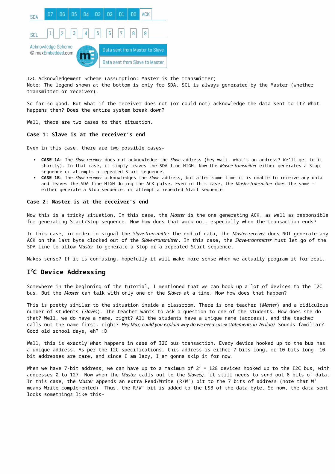
15 15, 32 Error16 16, 31 Init17 17, 36 Select In
18 to 25 18 to 30, 33 GND
- 34, 35 N/C
Table 1.0: Pin numbers and functions
Now let us know how communication between PC and printer takes place. Computer places the data in the data pins, then it makes the strobe low. When strobe goes low, printer understands that there is a valid data in data pins. Other pins are used to send controls to the printer and get status of the printer, you can understand them by the names assigned to the pins.
To use the printer port for applications other than printing, We need to know how ports are organized. There are three registers associated with LPT port: Data register, Control register and Status register. Data register will hold the data of the data pins of the port. That means, if we store a byte of data to the data register, that data will be sent to the data pins of the port. Similarly control and status registers. The following table explains how these registers are associated with ports.
Pin No (D-Type 25) SPP Signal Direction In/out Register.bit
1* nStrobe In/Out Control.02 Data 0 In/Out Data.03 Data 1 In/Out Data.14 Data 2 In/Out Data.25 Data 3 In/Out Data.36 Data 4 In/Out Data.47 Data 5 In/Out Data.58 Data 6 In/Out Data.69 Data 7 In/Out Data.7
10 nAck In Status.611* Busy In Status.712 Paper-Out / Paper-End In Status.513 Select In Status.414* nAuto-Linefeed In/Out Control.115 nError / nFault In Status.316 nInitialize In/Out Control.2
17* nSelect-Printer/ nSelect-In In/Out Control.3
18 - 25 Ground Gnd
Table 1.1: Pin directions and associated registers.
* Pins with * symbol in this table are hardware inverted. Than means, If a pin has a 'low' ie. 0V, Corresponding bit in the register will have value 1.
Signals with prefix 'n' are active low. That means, Normally these pins will have low value. When it needs to send some indication, it will become high. For example, Normally nStrobe will be high, when the data is placed in the port, computer makes that pin low.
Normally, data, control and status registers will have following addresses. We need these addresses in programming later.
Register LPT1 LPT2Data register (Base Address + 0) 0x378 0x278
Status register (Base Address + 1) 0x379 0x279Control register (Base Address + 2) 0x37a 0x27a
Note: All the parallel ports do not have bidirectional capability. Earlier parallel ports had only output enabled in data pins since printers only inputs data. But latter, to make parallel port capable of communicating with other devises, bidirectional ports are introduced.
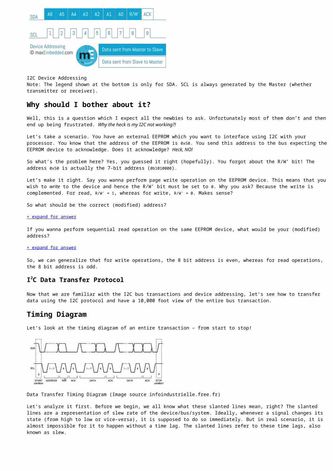
By default, data port is output port. To enable the bidirectional property of the port, we need to set the bit 5 of control register.
To know the details of parallel ports available in your computer, follow this procedure:
Right click on My Computer, go to "Properties". Select the tab Hardware, Click Device manager.
You will get a tree structure of devices; In that Expand "Ports(Com1 & LPT)".
Double Click on the ECP Printer Port(LPT1) or any other LPT port if available.
You will get details of LPT port. Make sure that "Use this Port (enable)" is selected.
Select tab recourses. In that you will get the address range of port.
To start programming, you will need a D-25 type Male connector. Its pin structures can be found in the connector as follows:
Programming the printer port in DOS:
To start programming the port, we will use DOS. In DOS we have commands to access the port directly. But, these programs will not work on the systems based on Windows XP, Windows NT or higher versions. For security reason, higher versions of the windows does not allow accessing the port directly. To program the parallel port in these systems, we need to write kernel mode driver. In the part II, I am going to explain about programming the parallel port in windows XP. If you want to run the same program in Windows XP, For studying you can use the technique that I have posted in this forum.
When we want to find out whether particular pin of the port is high or low, we need to input the value of corresponding register as a byte. In that, we have to find out whether the corresponding bit is high or low using bitwise operators. We can't access the pins individually. So, you need to know basic bitwise operations.
Main bitwise operators that we need are bitwise AND '&' and bitwise OR '|'. To make a particular bit in a byte high without affecting other bits, write a byte with corresponding bit 1 and all other bits 0; OR it with original byte. Similarly, to make particular bit low, write a byte with corresponding bit 0 and all other bits 1; AND it with original byte.
In Turbo C, there are following functions used for accessing the port:
outportb( PORTID, data); data = inportb( PORTID);
outport( PORTID, data);
data = inport( PORTID);
outport() function sends a word to port, inport() reads a word from the port. outportb() sends a byte to port and inportb() reads a byte from the port. If you include DOS.H header, these functions will be considured as macro, otherwise as functions. Function inport() will return a word having lower byte as data at PORTID and higher byte as data at PORTID+2. So, we can use this function to read status and control registers together. inportb() function returns byte at PORTID. outport() writes the lower byte to PORTID and higher byte to PORTID+1. So this can be used to write data and control together. outportb() function write the data to PORTID. outport() and outportb() returns nothing.
Let us start with inputting first. Here is an example program, copy it and run in Turbo C or Borland C without anything connected to parallel port. Then you should see data available in status register and pin numbers 10, 11, 12, 13 and 15 of the parallel port. Pin 11 (active low) is 0 and all other pins are 1 means it is OK.
/* file: ex1.c by HarshaPerla for electroSofts.com. Displays contents of status register of parallel port. Tested with TurboC 3.0 and Borland C 3.1 for DOS.*/
#include"stdio.h"#include"conio.h"#include"dos.h"
#define PORT 0x378
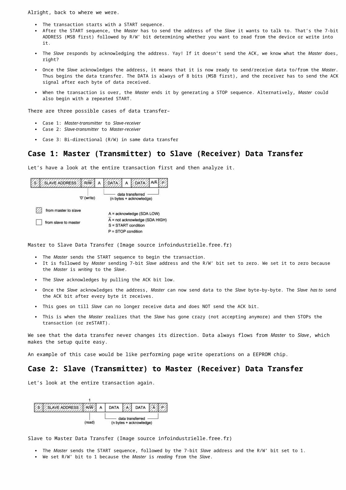
void main(){ int data; clrscr(); while(!kbhit()) { data=inportb(PORT+1); gotoxy(3,10); printf("Data available in status register: %3d (decimal), %3X (hex)\n", data, data); printf("\n Pin 15: %d",(data & 0x08)/0x08); printf("\n Pin 13: %d",(data & 0x10)/0x10); printf("\n Pin 12: %d",(data & 0x20)/0x20); printf("\n Pin 11: %d",(data & 0x80)/0x80); printf("\n Pin 10: %d",(data & 0x40)/0x40); delay(10); }}
To understand bitwise operations: you want to find data in pin 15, value of (data & 0x08) will be 0x08 if bit 3 of register is high, 0therwise.
bit no. 7654 3210 data : XXXX 1XXX & with : 0000 1000 (0x08 ) -> 0000 1000 (0x08 -> bit 3 is high )
bit no. 7654 3210 data : XXXX 0XXX & with : 0000 1000 (0x08 ) -> 0000 0000 (0x00 -> bit 3 is low)
We will use the same logic throughout the article.
Now, take a D-25 male with cables connected to each pins. Short all the pins from 18 to 25, call it as ground. Now you can run above program and see the change by shorting pins 10, 11, 12, 13 and 15 to ground. I prefer using switches between each input pins and ground. Be careful, do not try to ground the output pins.
To find out the availability of ports in a computer programmatically, we will use the memory location where the address of port is stored.
0x408 0x409 0x40a 0x40b 0x40c 0x40d
LPT1 lowbyte
LPT1 highbyte
LPT2 lowbyte
LPT2 highbyte
LPT3 lowbyte
LPT3highbyte
If you run the the following code in Turbo C or Borland C, You will get the addresses of available ports.
/*PortAdd.c To find availability and addresses of the lpt ports in the computer.
*/
#include <stdio.h>#include <dos.h>void main(){ unsigned int far *ptraddr; /* Pointer to location of Port Addresses */ unsigned int address; /* Address of Port */ int a; ptraddr=(unsigned int far *)0x00000408; clrscr();
for (a = 0; a < 3; a++) { address = *ptraddr; if (address == 0) printf("No port found for LPT%d \n",a+1); else printf("Address assigned to LPT%d is 0x%X \n",a+1,address); ptraddr++; } getch();}
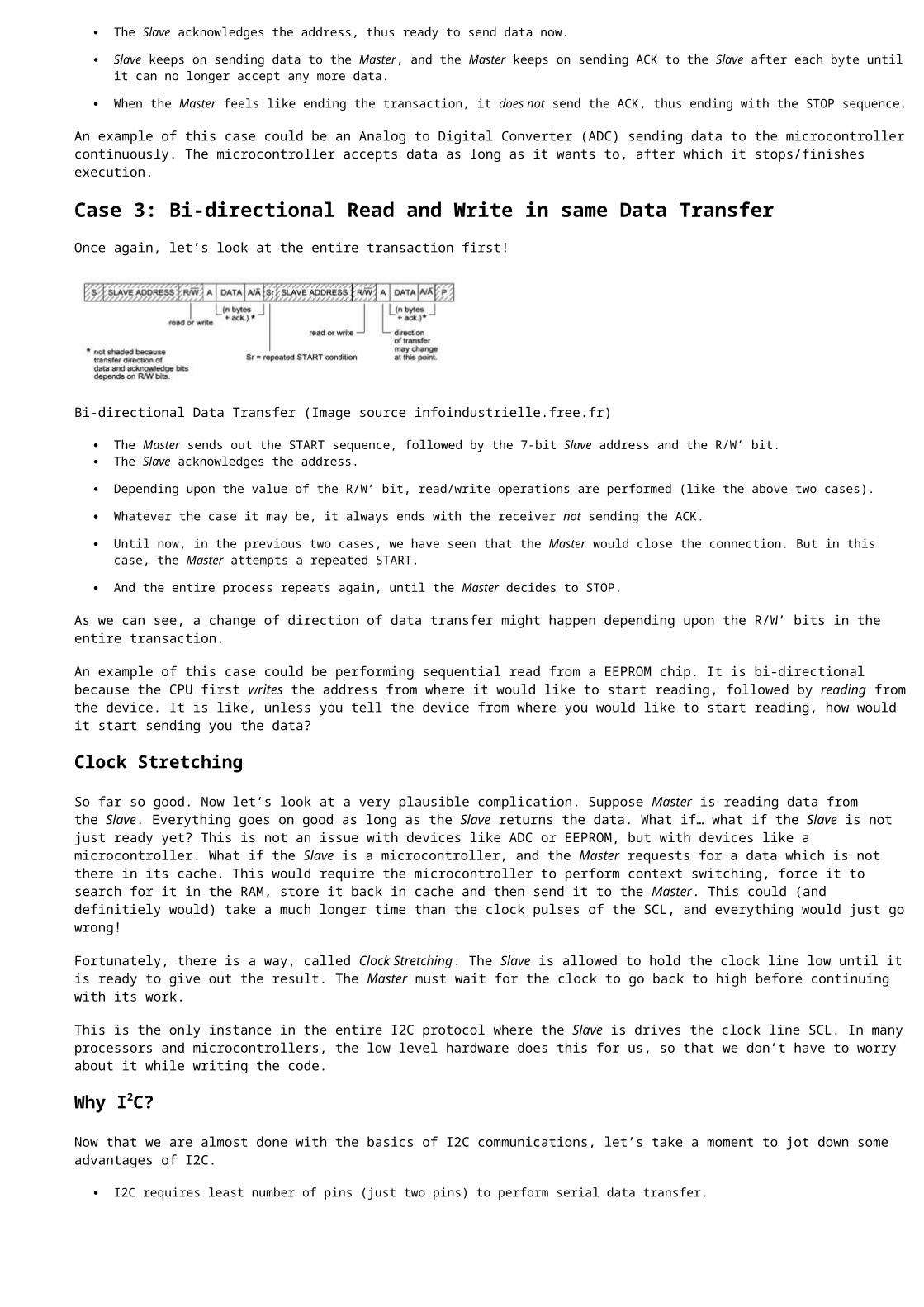
Next we will go to check output pins. To check the output, we will use LED's. I have driven LED's directly from the port. But it is preferred to connect a buffer to prevent excessive draw of current from the port. Connect an LED in series with a resister of 1KW or 2.2KW between any of the data pins(2 to 9) and ground. With that, if you run the program given below, you should see the LED blinking with app. 1 sec frequency.
#include"conio.h"#include"dos.h"
#define PORT 0x378
void main(){ while(!kbhit()) { outportb(PORT, ~inportb(PORT) ); delay(1000); }}
I will stop this part here itself. Next part of this article is now ready. In the PART 2, you will learn programming the parallel port in VC++. PART 2 is designed for the beginners of VC++. Click here to Read part 2.
Part 3 is having the example using LCD module. There we are going to learn connecting LCD module to parallel port. Read part 3.
Also Read...
-Programming the Parallel Port(PART 2): with VC++-Programming the 16x2 LCD module with Parallel Port: Example 1-PC Based Game show/Quiz buzzer: Interfacing project example 2-Serial communication via RS232 with C-Links to port programming related articles in other sites
Introduction to RS-232:
RS232 is the most known serial port used in transmitting the data in communication and interface. Even though serial port is harder to program than the parallel port, this is the most effective method in which the data
transmission requires less wires that yields to the less cost. The RS232 is the communication line which enables the data transmission by only using three wire links. The three links provides ‘transmit’, ‘receive’ and common ground...
The ‘transmit’ and ‘receive’ line on this connecter send and receive data between the computers. As the name indicates, the data is transmitted serially. The two pins are TXD & RXD. There are other lines on this port as RTS, CTS, DSR, DTR, and RTS, RI. The ‘1’ and ‘0’ are the data which defines a voltage level of 3V to 25V and -3V to -25V respectively.
The electrical characteristics of the serial port as per the EIA (Electronics Industry Association) RS232C Standard specifies a maximum baud rate of 20,000bps, which is slow compared to today’s standard speed. For this reason, we have chosen the new RS-232D Standard, which was recently released.
The RS-232D has existed in two types. i.e., D-TYPE 25 pin connector and D-TYPE 9 pin connector, which are male connectors on the back of the PC. You need a female connector on your communication from Host to Guest computer. The pin outs of both D-9 & D-25 are show below.
D-Type-9 pin no.
D-Type-25 pin no.
Pin outs Function
3 2 RD Receive Data (Serial data input)
2 3 TD Transmit Data (Serial data output)
7 4 RTS Request to send (acknowledge to modem that UART is ready to exchange data
8 5 CTS Clear to send (i.e.; modem is ready to exchange data)
6 6 DSR Data ready state (UART establishes a link)
5 7 SG Signal ground
1 8 DCD Data Carrier detect (This line is active when modem detects a carrier
4 20 DTR Data Terminal Ready.
9 22 RI Ring Indicator (Becomes active when modem detects ringing signal from PSTN
About DTE & DCE :
Devices, which use serial cables for their communication, are split into two categories. These are DCE (Data Communications Equipment) and DTE (Data Terminal Equipment.) Data Communications Equipments are devices such as your modem, TA adapter, plotter etc while Data Terminal Equipment is your Computer or Terminal. A typical Data Terminal Device is a computer and a typical Data Communications Device is a Modem. Often people will talk about DTE to DCE or DCE to DCE speeds. DTE to DCE is the speed between your modem and computer, sometimes referred to as your terminal speed. This should run at faster speeds than the DCE to DCE speed. DCE to DCE is the link between modems, sometimes called the line speed.
Most people today will have 28.8K or 33.6K modems. Therefore, we should expect the DCE to DCE speed to be either 28.8K or 33.6K. Considering the high speed of the modem we should expect the DTE to DCE speed to be about 115,200 BPS. (Maximum Speed of the 16550a UART) . The communications program, which we use, has settings for DCE to DTE speeds. However, the speed is 9.6 KBPS, 144 KBPS etc and the modem speed.
If we were transferring that text file at 28.8K (DCE- DCE), then when the modem compresses it you are actually transferring 115.2 KBPS between computers and thus have a DCE- DTE speed of 115.2 KBPS. Thus, this is why the DCE- DTE should be much higher than the modem's connection speed. Therefore, if our DTE to DCE speed is several times faster than our DCE to DCE speed the PC can send data to your modem at 115,200 BPS.
What is NULL MODEM ?
Null modem is used to connect two DTE's together. This is used to transfer files between the computers using protocols like Zmodem protocol, xmodem protocol, etc
Figure: Above shows the connections of the Null modem using RS-232D connecter
Above-mentioned figure shows the wiring of the null modem. The main feature indicated here is that the to make the computer to chat with the modem rather than another computer. The guest & host computer connected through the TD, RD, and SG pins. Any data that is transmitted through TD line from the Host to Guest is received on RD line. The Guest computer must have the same setup as the Host. The signal ground (SG) line of the both must be shorted so that grounds are common to each computer.
The Data Terminal Ready (DTR) is looped back to Data Set Ready and Carrier Detect on both computers. When the Data Terminal Ready is asserted active, then the Data Set Ready and Carrier Detect immediately become active. At this point, the computer thinks the Virtual Modem to which it is connected is ready and has detected the carrier of the other modem.
All left to worry about now is the Request to Send and Clear To Send. As both computers communicate together at the same speed, flow control is not needed thus these two lines are also linked together on each computer. When the computer wishes to send data, it asserts the Request to Send high and as it is hooked together with the Clear to Send, It immediately gets a reply that it is ok to send and does so.
The Ring indicator line is only used to tell the computer that there is a ringing signal on the phone line. As we do not have, a modem connected to the phone line this is left disconnected
To know about the RS232 ports available in your computer, Right click on "My Computer", Goto 'Properties', Select tab 'Device Manager', go to Ports( COM & LPT ), In that you will find 'Communication Port(Com1)' etc. If you right click on that and go to properties, you will get device status. Make sure that you have enabled the port( Use this port is selected).
How to program the Serial Port using C/C++ ?
There are two popular methods of sending data to or from the serial port in Turbo C. One is using outportb(PORT_ID, DATA) or outport(PORT_ID,DATA) defined in “dos.h”. Another method is using bioscom() function defined in “bios.h”.
Using outportb() :
The function outportb () sends a data byte to the port ‘PORT_ID’. The function outport() sends a data word. These functions can be used for any port including serial port, parallel ports. Similarly to receive data these are used.
inport reads a word from a hardware port inportb reads a byte from a hardware port
outport outputs a word to a hardware port
outportb outputs a byte to a hardware port
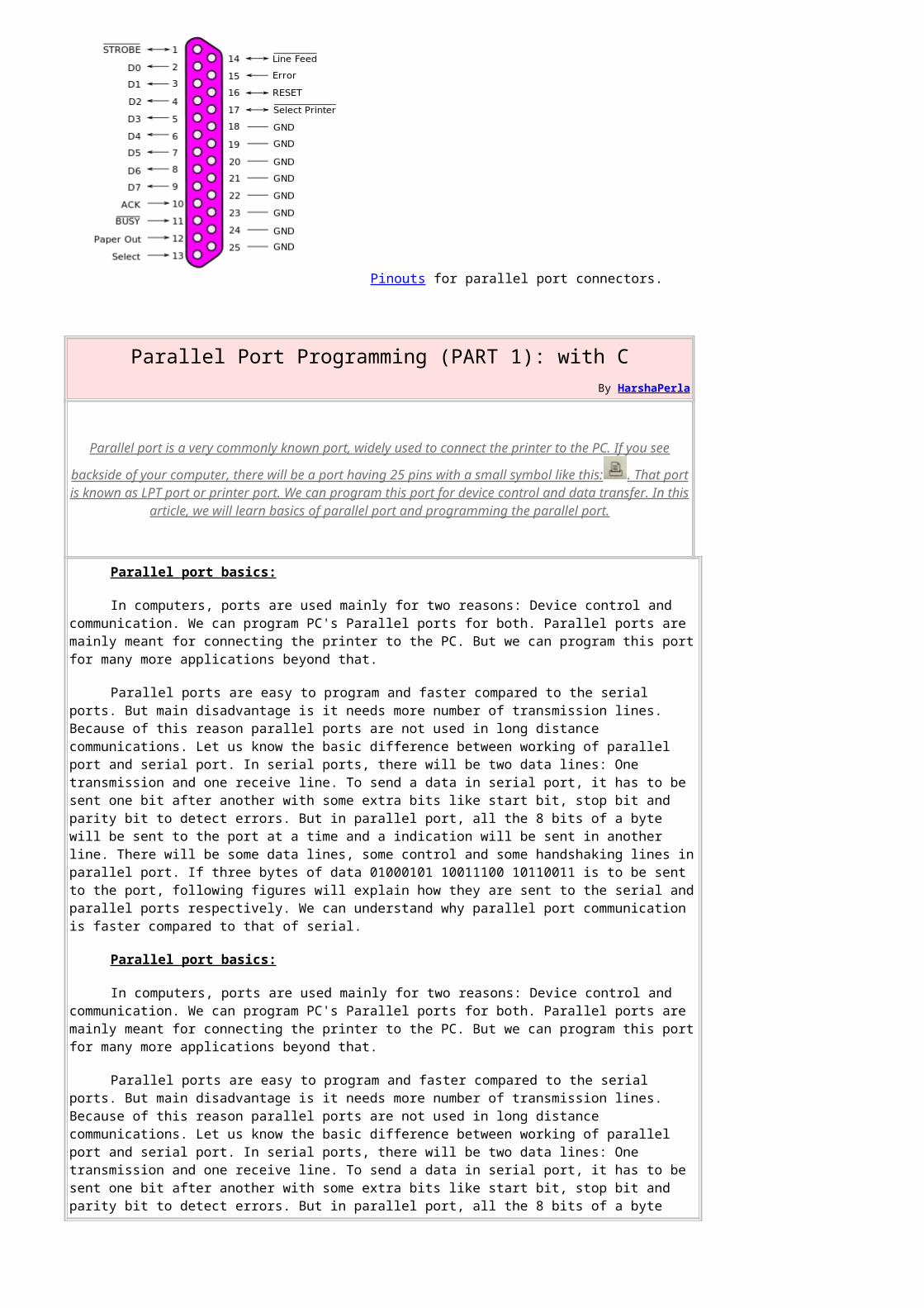
Declaration:
int inport(int portid); unsigned char inportb(int portid);
void outport(int portid, int value);
void outportb(int portid, unsigned char value);
Remarks:
inport works just like the 80x86 instruction IN. It reads the low byte of a word from portid, the high byte from portid + 2. inportb is a macro that reads a byte
outport works just like the 80x86 instruction OUT. It writes the low byte of value to portid, the high byte to portid + 1.
outportb is a macro that writes value Argument
portid:
Inport- port that inport and inportb read from; Outport- port that outport and outportb write to
value:
Word that outport writes to portid; Byte- that outportb writes to portid.
If you call inportb or outportb when dos.h has been included, they are treated as macros that expand to inline code.
If you don't include dos.h, or if you do include dos.h and #undef the macro(s), you get the function(s) of the same name.
Return Value:
# inport and inportb return the value read
# outport and outportb do not return
For more details of these functions read article from beondlogic.com
Using bioscom:
The macro bioscom () and function _bios_serialcom() are used in this method in the serial communication using RS-232 connecter. First we have to set the port with the settings depending on our need and availability. In this method, same function is used to make the settings using control word, to send data to the port and check the status of the port. These actions are distinguished using the first parameter of the function. Along with that we are sending data and the port to be used to communicate.
Here are the deatails of the Turbo C Functions for communication ports.
Declaration:
bioscom(int cmd, char abyte, int port) _bios_serialcom(int cmd ,int port, char abyte)
bioscom() and _bios_serialcom() uses the bios interrupt 0x14 to perform various communicate the serial communication over the I/O ports given in port.
cmd: The I/O operation to be performed.
cmd (boiscom) cmd(_bios_serialcom)Action0 _COM_INIT Initialise the parameters to the port1 _COM_SEND Send the character to the port
2 _COM_RECEIVE Receive character from the port
3 _COM_STATUS Returns rhe current status of the communication port
portid: port to which data is to be sent or from which data is to be read.
0: COM11: COM22: COM3
abyte:
When cmd =2 or 3 (_COM_SEND or _COM_RECEIVE) parameter abyte is ignored.
When cmd = 0 (_COM_INIT), abyte is an OR combination of the following bits (One from each group):
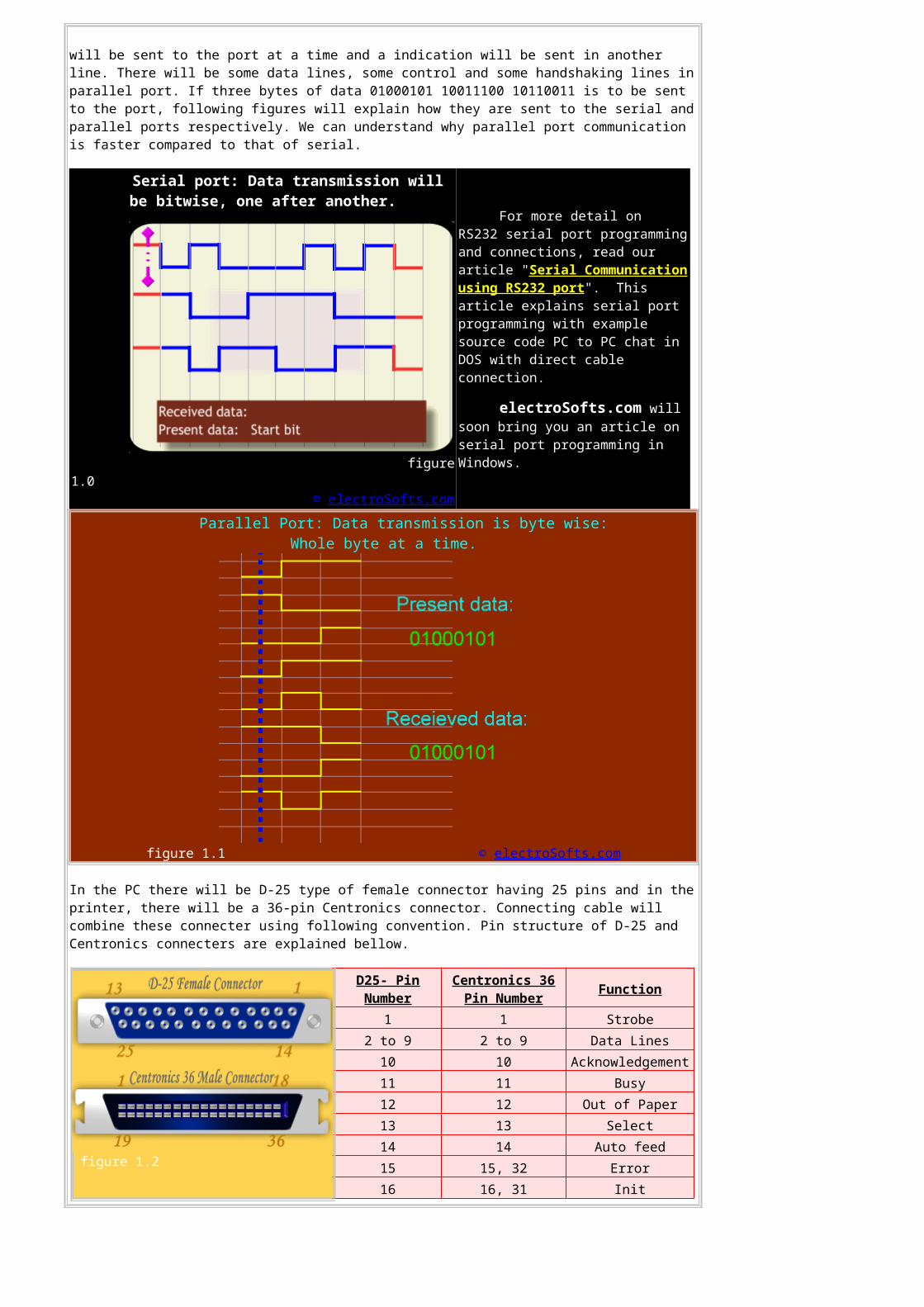
value of abyte Meaning
Bioscom _bios_serialcom
0x02
0x03
_COM_CHR7
_COM_CHR8
7 data bits
8 data bits0x00
0x04
_COM_STOP1
_COM_STOP2
1 stop bit
2 stop bits0x00
0x08
0X10
_COM_NOPARITY
_COM_ODDPARITY
_COM_EVENPARITY
No parity
Odd parity
Even parity0x00
0x20
0x40
0x60
0x80
0xA0
0xC0
0xE0
_COM_110
_COM_150
_COM_300
_COM_600
_COM_1200
_COM_2400
_COM_4800
_COM_9600
110 baud
150 baud
300 baud
600 baud
1200 baud
2400 baud
4800 baud
9600 baud
For example, if
abyte = 0x8B = (0x80 | 0x08 | 0x00 | 0x03) = (_COM_1200 | _COM_ODDPARITY | _COM_STOP1 | _COM_CHR8)
the communications port is set to 1200 baud (0x80 = _COM_1200) Odd parity (0x08 = _COM_ODDPARITY) 1 stop bit (0x00 = _COM_STOP1) 8 data bits (0x03 = _COM_CHR8)
To initialise the port with above settings we have to write,
bioscom(0, 0x8B, 0);
To send a data to COM1, the format of the function will be bioscom(1, data, 0). Similarly bioscom(1, 0, 0 ) will read a data byte from the port.
The following example illustrate how to serial port programs. When a data is available in the port, it inputs the data and displays onto the screen and if a key is pressed the ASCII value will be sent to the port.
#include <bios.h>#include <conio.h>#define COM1 0#define DATA_READY 0x100#define SETTINGS ( 0x80 | 0x02 | 0x00 | 0x00)int main(void){ int in, out, status; bioscom(0, SETTINGS, COM1); /*initialize the port*/ cprintf("Data sent to you: "); while (1) { status = bioscom(3, 0, COM1); /*wait until get a data*/ if (status & DATA_READY) if ((out = bioscom(2, 0, COM1) & 0x7F) != 0) /*input a data*/ putch(out); if (kbhit()) { if ((in = getch()) == 27) /* ASCII of Esc*/ break; bioscom(1, in, COM1); /*output a data*/ } } return 0;}
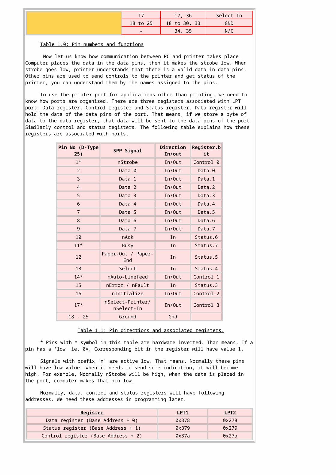
When you compile and run the above program in both the computers, The characters typed in one computer should appear on the other computer screen and vice versa. Initially, we set the port to desired settings as defined in macro settings. Then we waited in an idle loop until a key is pressed or a data is available on the port. If any key is pressed, then kbhit() function returns non zero value. So will go to getch function where we are finding out which key is pressed. Then we are sending it to the com port. Similarly, if any data is available on the port, we are receiving it from the port and displaying it on the screen.
To check the port, If you have a single computer, you can use loop-back connection as follows. This is most commonly used method for developing communication programs. Here, data is transmitted to that port itself. Loop-back plug connection is as follows.
Fig 2. Loop-back plug connection
If you run the above program with the connection as in this diagram, the character entered in the keyboard should be displayed on the screen. This method is helpful in writing serial port program with single computer. Also you can make changes in the port id if your computer has 2 rs232ports. You can connect the com1 port to com2 of the same computer and change the port id in the program. The data sent to the port com1 should come to port com2. then also whatever you type in the keyboard should appear on the screen.
The program given below is an example source code for serial communication programmers. It is a PC to PC communication using RS232. Download the code, unzip and run to chat in dos mode between two computers. Use the program to get more idea about serial port programming.
Click here to download example source code: pc2pc.zip
Please contact us if any problem exits in the above programs.
>Interfacing Links:L inks related to serial port, bioscom function, rs232, rs485, usb, parallel port etc. >Click here to list other C Programming sites
Click here to send feedback or use email: [email protected] or [email protected]
Note: Examples given above are tested with Turbo C++ Compiler Version 3.0. How ever, we do not give any guaranty for working of the programs in the examples.
Parallel port programming
We can easily program the parallel port in DOS. But as we know, DOS programs have their own limitations. So, if you want to move from DOS
to Windows, go through this article. This is an introduction to program the parallel port in VC++. You need not have much knowledge about
VC++. This article is designed for one who know basics of parallel port and beginners of VC++. If you don't know anything about parallel port,
read my first article "Parallel port programming with C (Part 1)". There you get basic information about parallel port and programming the port in
Turbo C or Borland C.
Now, you are knowing the pins and registers of parallel port. You know how to access them in DOS. If you want to run your program in
Windows 95 or 98, you are having access to the port in the similar way. You need to know how to use dialog boxes and windows materials with
it. But your program should also run in Windows XP, NT or higher versions, then there is another issue. Higher versions of Windows do not
allow to access the hardware directly for security reasons. But still, there are ways, I will explain later. First we will start programming which will
work only in lover versions of Windows.
Direct Access:
If you want to program the port in VB, there is no direct access to the port. Still you can access the port using DLL files created with VC++.
You can use the next method Access using inpout32.
If you are familiar with Visual C++, then create a dialog based application named ParallelPort and skip this section, go to adding controls.
Creating the application:
Start Visual C++, Select File->New.
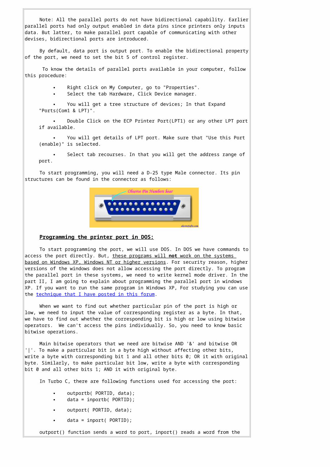
In the tab 'Projects', Select "MFC AppWizard (exe)", give project name as "ParallelPort" and click OK.
In the next window, select radio button "Dialog based" and click next leaving all other options default.
Click Finish, then OK to get a window with two buttons and one sentence "TODO: Place Dialog controls here.", select and delete that
sentence. Click to select the button "Cancel" and delete it.
Right click on button labeled OK, select Properties from the drop down menu. Change the value of Caption to "&EXIT" from "OK".
Resize the dialog box to get a window as shown below. If you run the application by clicking this icon: , it should give 0 errors and 0
warnings, and you will get the following window.
figure(2.1)
Adding controls:
Now, you should see a tool bar as shown here, it is called Control toolbar. If not, select
it from view menu->toolbars. Icon marked here with red color is the Check Box. If you click
the check box icon and draw in the window, You will have the check box placed in the
window. You need to place 17 such check boxes in the window. You can use copy-past to
make your work easy. After that, Group then using 3 group boxes. Group box icon is there
above the check box in the figure. After doing this much, your design should look like
figure(2.3). So, re arrange your dialog components to look like that. Again run the
application and make sure that there is no error. figure(2.2)
Figure(2.3)
Next, right click on the Group Box labeled Static and go to properties. Change the captions to Data, Status and Control respectively. Right
click on the first Check box Check 1, Change the caption to "Pin 2" and ID to IDC_Pin2. Similarly change the captions of check boxes in data
group to Pin 2 to Pin 9; status port Pin 10, Pin 11, Pin 12, Pin 13 and Pin 15; Control Port Pin 1, Pin 14, Pin 16 and Pin 17. Change the ID's
correspondingly(IDC_Pin2, IDC_Pin3...).
Window designing is over. Next part is coding. We have placed some controls in the dialog box. To get the values of these controls, we
need to have variables associated with then. To do that, right click and select "ClassWizard" from drop down menu. Select tab "Member
Variables". You will get a list of Control IDs. Select each IDs separately and click Add Variable. Type variable name as m_pin1. m_pin10,
m_pin11... and retain Category Value and Variable type BOOL. Refer following figure.
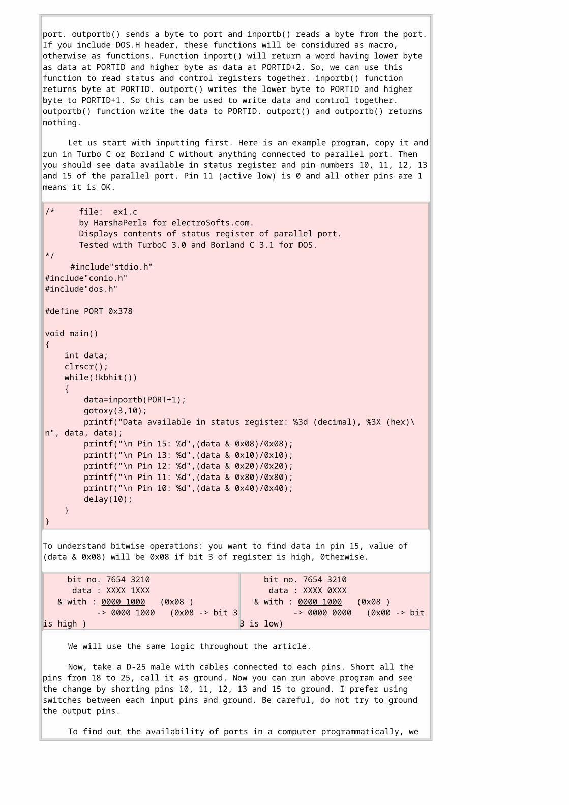
Figure(2.4)
In the Workspace, Select ClassView tab, under ParallelPort classes, right click on CParallelPortDlg, click Add Member Function. Give function type as
void and function name as UpdatePins(). It will take you to the new function created. Edit the code as follows.
void CParallelPortDlg::UpdatePins(){ int reg; reg=_inp(STATUS);
if((reg & 0x40)==0) m_pin10=0; else m_pin10=1; if((reg & 0x80)==0) m_pin11=0; else m_pin11=1; if((reg & 0x20)==0) m_pin12=0; else m_pin12=1;
if((reg & 0x10)==0) m_pin13=0; else m_pin13=1; if((reg & 0x08)==0) m_pin15=0; else m_pin15=1; ////////// reg=_inp(DATA); if((reg & 0x01)==0) m_pin2=0; else m_pin2=1; if((reg & 0x02)==0) m_pin3=0; else m_pin3=1; if((reg & 0x04)==0) m_pin4=0; else m_pin4=1; if((reg & 0x08)==0) m_pin5=0; else m_pin5=1; if((reg & 0x10)==0) m_pin6=0; else m_pin6=1; if((reg & 0x20)==0) m_pin7=0; else m_pin7=2; if((reg & 0x40)==0) m_pin8=0; else m_pin8=1; if((reg & 0x80)==0) m_pin9=0; else m_pin9=1; ////// reg = _inp(CONTROL);
if((reg & 0x01)==0) m_pin1=0; else m_pin1=1; if((reg & 0x02)==0) m_pin14=0; else m_pin14=1; if((reg & 0x04)==0) m_pin16=0; else m_pin16=1; if((reg & 0x08)==0) m_pin17=0; else m_pin17=1;
UpdateData(FALSE);}
Now scroll to the top of the page and add these lines before class declarations.
#define DATA 0x378#define STATUS 0x379#define CONTROL 0x37a
The function CParallelPortDlg::UpdatePins() is used to display values of all pins initially. Here, we have used _inp() function to get the
values of registers associated with the ports. _inp(PORT) will return the data present in PORT. Depending on the status of the pins, we are
making Check boxes checked or unchecked. When we change the value of member variable and call the function UpdateData(FALSE), the
values in the member variables will be updated in the corresponding controls in the window. Similarly if you call UpdateData(TRUE), Values
which are there in the corresponding controls will sit in the member variables. Here, The values from the variables should be updated in the
window. So, UpdateWindow(FALSE). If you have read my first article, you will understand all other things done here.
To make run this code when the dialog is initialized, we need to call it. So, go to function OnInitdialog() in the file CParallelPortDlg. (In the class view
tab of the workspace, under ParallelPort Classes, expand CParallelPortDlg, you will get the function name, double click it.) Add the following code to it. This
code will call the function UpdatePins() and set a timer to scan the port pins. You can change the second parameter to change the frequency at which ports are
needed to be scanned. I have used 200 milli seconds. _outp(CONTROL, 0xDF) will reset the control register bit 5 low so that data pins will act as output.
_outp(PORT, DATA) sends the byte DATA to the address PORT.
BOOL CParallelPortDlg::OnInitDialog(){
//App.Wiz generated code // TODO: Add extra initialization here SetTimer(1,200,NULL); _outp(CONTROL, _inp(CONTROL) & 0xDF); UpdatePins(); return TRUE; // return TRUE unless you set the focus to a control}
Next part is Updating the pin contents for each timer tics. For that, we need to handle the windows message WM_TIMER. Now since we have set the
timer for 200 ms, for every 200 ms, Windows returns WM_TIMER message. To write a handler, write click on the CParallelPortDlg in the class view tab,
select "Add Windows Message Handler...". In "New Windows messages/events", select WM_TIMER and click Add and Edit. It will take you to the newly
created function CParallelPortDlg::OnTimer(UINT nIDEvent). Add the following code to it.
void CParallelPortDlg::OnTimer(UINT nIDEvent) { // TODO: Add your message handler code here and/or call default int status_reg; status_reg=_inp(STATUS); if((status_reg & 0x40)==0) m_pin10=0; else m_pin10=2; if((status_reg & 0x80)==0) m_pin11=0; else m_pin11=1; if((status_reg & 0x20)==0) m_pin12=0; else m_pin12=1; if((status_reg & 0x10)==0) m_pin13=0; else m_pin13=1; if((status_reg & 0x08)==0) m_pin15=0; else m_pin15=1;
UpdateData(FALSE); CDialog::OnTimer(nIDEvent);}
Here, we have refreshed only input pins. Output pins have to be changed when user clicks on the check boxes. To find any change of
value in check boxes, we can use BN_CLICKED message handler. But for all the check boxes we have to repeat the process. It is easy to use
ON_COMMAND_RANGE. For that, scroll up to the position in the file ParallelPortDlg.cpp where you find
BEGIN_MESSAGE_MAP(CParallelPortDlg, CDialog). (Do not confuse between CParallelPortDlg and CAboutDlg.) Add the following code to it.
BEGIN_MESSAGE_MAP(CParallelPortDlg, CDialog) //{{AFX_MSG_MAP(CParallelPortDlg) ON_WM_SYSCOMMAND() ON_WM_PAINT() ON_WM_QUERYDRAGICON() ON_WM_TIMER() //}}AFX_MSG_MAP //Code added by me from here. ON_COMMAND_RANGE(IDC_Pin2, IDC_Pin9, ChangePin) ON_COMMAND(IDC_Pin14, ChangeControl) ON_COMMAND(IDC_Pin16, ChangeControl) ON_COMMAND(IDC_Pin17, ChangeControl) ON_COMMAND(IDC_Pin1, ChangeControl) //Code added by me till hereEND_MESSAGE_MAP()
Above code will call the function ChangePin() when buttons in the range IDC_Pin2 to IDC_Pin9 are changed and ChangeControl() when chack buttons
with ID IDC_Pin14, IDC_Pin16, IDC_Pin17 or IDC_Pin1 are changed. Now we need those two functions. Add two new functions to CParllelPortDlg: void
'ChangePin()' and 'void ChangeControl()' using the method explained earlier. Write codes to them as follows:
void CParallelPortDlg::ChangePin(int pin){
int data_register, new_register;
UpdateData(TRUE);data_register=_inp( DATA );new_register=0;if( m_pin2==TRUE ) new_register |= 0x01;if( m_pin3==TRUE ) new_register |= 0x02;if( m_pin4==TRUE ) new_register |= 0x04;
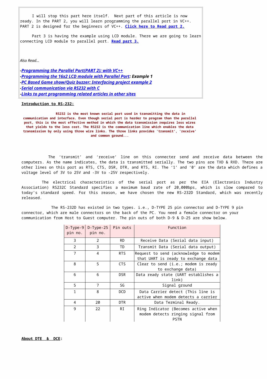
if( m_pin5==TRUE ) new_register |= 0x08;if( m_pin6==TRUE ) new_register |= 0x10;if( m_pin7==TRUE ) new_register |= 0x20;if( m_pin8==TRUE ) new_register |= 0x40;if( m_pin9==TRUE ) new_register |= 0x80;
_outp(DATA, new_register);
}
void CParallelPortDlg::ChangeControl(){
int control_register, new_register;
UpdateData(TRUE);
control_register = _inp( CONTROL );new_register = control_register;
if( m_pin1== 0 ) new_register &= 0xFE; else new_register |= 0x01; if( m_pin14==0 ) new_register &= 0xFD; else new_register |= 0x02; if( m_pin16==0 ) new_register &= 0xFB; else new_register |= 0x04; if( m_pin17==0 ) new_register &= 0xF7; else new_register |= 0x08;
_outp(CONTROL, new_register);
}
If everything is OK, you should get the following window when you run the program. To test the program, run this program without
connecting anything to the port. Change some of the pins and close the window. If you run the program again you should get the values which
was there before closing the window in the output pins.
You can always use this program to test the parallel port. Now, make a circuit connecting all the input pins to switches, all the output pins to LEDs with
2.2K or 10K resisters. If you press switch, corresponding pin value should change in the screen, If you change state of any output pin, corr
esponding LED should glow.
Every thing is ok. But as you know, this program will run only in win9x. If your program is needed to run in
windows xp and higher versions, you need to write a kernel mode device driver. Do not worry if you are not up to
that level. There are DLL files available freely for such drivers. You can use those files and call them from your
program.
Access using inpout32
If you do not want to use driver and test the above program in Windows XP as it is, use my post in the ElectroSofts
Forum
InpOut32 is a DLL file which can send a data to parallel port and which can return the data in the parallel port.
You can download this file with source code for free from http://logix4u.net. You can use this file in any windows
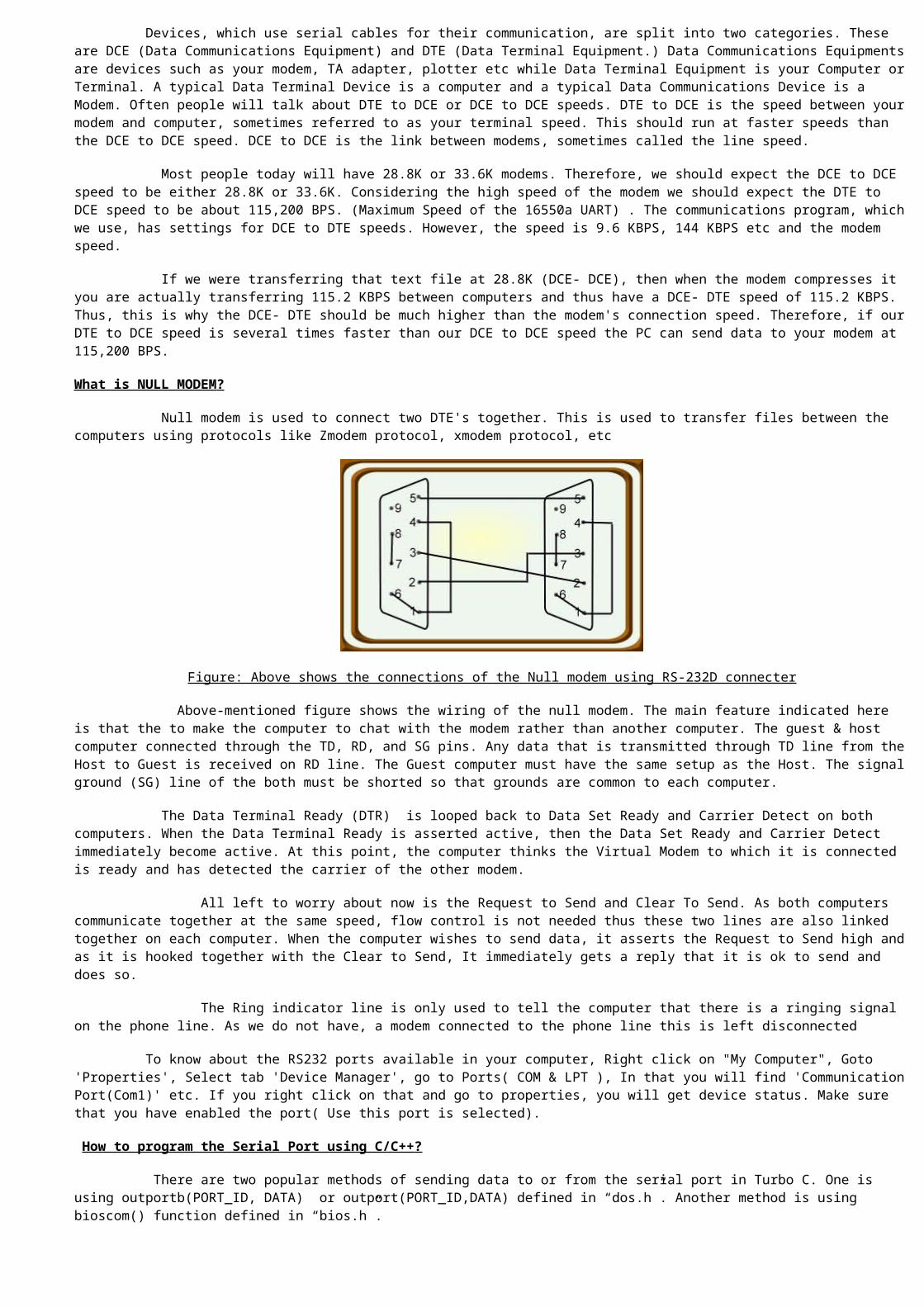
programming language like Visual basic, C#, C++ etc. If you know how to use DLL files, download the file from
http://logix4u.net and use Inp32() and Out32() functions instead of _inp() and _outp().
To know how to use DLL file in VC++, let us now convert our previous project to XP enabled program.
Add these two lines in the file ParallelPortDlg.cpp after pre processor directives.
short _stdcall Inp32(short portaddr);void _stdcall Out32(short portaddr, short datum);
Where ever _inp() comes, change them to Inp32() and where ever outp() comes, change them to Out32().
Copy DLL file inpout32.dll and lib file inpout32.lib got by compiling the source code available at logix4u.net
to the project folder.
From project menu, select settings, go to tab link, in object/ library modules write inpout32.lib
Now your program should run without any errors.
If you have any comment, feedback and suggestions, please send an e-mail to [email protected] or use
this feedback form
To discuss the Interfacing related issues, use Electrosofts Forum
Also Read:
-(next part)Interfacing example: LCD module-Programming the parallel Port(Part 1) with C(DOS)-Serial Communication via RS232 with C-Port programming tutorials in other sites
ISA/PCI PROTOCOLS
PCI Slots and PCI card
PIC protocol
PCI is synchronous bus architecture with all data transfers being performed relative to a system clock (CLK). The initial PCI specification permitted a maximum clock rate of 33 MHz allowing one bus transfer to be performed every 30 nanoseconds. Later, PCI specification extended the bus definition to support operation at 66 MHz, but the vast majority of today’s personal computers continue to implement a PCI bus that runs at a maximum speed of 33 MHz.
PCI implements a 32-bit multiplexed Address and Data bus (AD[31:0]). It architects a means of supporting a 64-bit data bus through a longer connector slot, but most of today’s personal computers support only 32-bit data transfers through the base 32-bit PCI connector. At 33 MHz, a 32-bit slot supports a maximum data transfer rate of 132 MBytes/sec, and a 64-bit slot supports 264 MBytes/sec.
The multiplexed Address and Data bus allows a reduced pin count on the PCI connector that enables lower cost and smaller package size for PCI components. Typical 32-bit PCI add-in boards use only about 50 signals pins on the PCI connector of which 32 are the multiplexed Address and Data bus. PCI bus cycles are initiated by driving an address onto the AD[31:0] signals during the first clock edge called the address phase. The address phase is signaled by the activation of the FRAME# signal. The next clock edge begins the first of one or more data phases in which data is transferred over the AD[31:0] signals.
In PCI terminology, data is transferred between an initiator which is the bus master, and a target which is the bus slave. The initiator drives the C/BE[3:0]# signals during the address phase to signal the type of transfer (memory read, memory write, I/O read, I/O write, etc.). During data phases the C/BE[3:0]# signals serve as byte enable to indicate which data bytes are valid. Both the initiator and target may insert wait states into the data transfer by deasserting the IRDY# and TRDY# signals. Valid data transfers occur on each clock edge in which both IRDY# and TRDY# are asserted.
A PCI bus transfer consists of one address phase and any number of data phases. I/O operations that access registers within PCI targets typically have only a single data phase. Memory transfers that move blocks of data consist of multiple data phases that read or write multiple consecutive memory locations. Both the initiator and target may terminate a bus transfer sequence at any time. The initiator signals completion of the bus transfer by deasserting the FRAME# signal during the last data phase. A target may terminate a bus transfer by asserting the STOP# signal. When the initiator detects an active STOP# signal, it must terminate the current bus transfer and re-arbitrate for the bus before continuing. If STOP# is asserted without any data phases completing, the target has issued a retry. If STOP# is asserted after one or more data phases have successfully completed, the target has issued a disconnect.
Initiators arbitrate for ownership of the bus by asserting a REQ# signal to a central arbiter. The arbiter grants ownership of the bus by asserting the GNT# signal. REQ# and GNT# are unique on a per slot basis allowing the arbiter to implement a bus fairness algorithm. Arbitration in PCI is “hidden” in the sense that it does not consume clock cycles. The current initiator’s bus transfers are overlapped with the arbitration process that determines the next owner of the bus.
PCI supports a rigorous auto configuration mechanism. Each PCI device includes a set of configuration registers that allow identification of the type of device (SCSI, video, Ethernet, etc.) and the company that produced it. Other registers allow configuration of the device’s I/O addresses, memory addresses, interrupt levels, etc.
Although it is not widely implemented, PCI supports 64-bit addressing. Unlike the 64-bit data bus option which requires a longer connector with additional 32-bits of data signals, 64-bit addressing can be supported through the base 32-bit connector. Dual Address Cycles are issued in which the low order 32-bits of the address are driven onto the AD[31:0] signals during the first address phase, and the high order 32-bits of the address (if non-zero) are driven onto the AD[31:0] signals during a second address phase. The remainder of the transfer continues like a normal bus transfer.
PCI defines support for both 5 Volt and 3.3 Volt signaling levels. The PCI connector defines pin locations for both the 5 Volt and 3.3 Volt levels. However, most early PCI systems were 5 Volt only, and did not provide active power on the 3.3 Volt connector pins. Over time more use of the 3.3 Volt interface is expected, but add-in boards which must work in older legacy systems are restricted to using only the 5 Volt supply. A “keying” scheme is implemented in the PCI connectors to prevent inserting an add-in board into a system with incompatible supply voltage.
Although used most extensively in PC compatible systems, the PCI bus architecture is processor independent. PCI signal definitions are generic allowing the bus to be used in systems based on other processor families. PCI includes strict specifications to ensure the signal quality required for operation at 33 and 66 MHz. Components and add-in boards must include unique bus drivers that are specifically designed for use in a PCI bus environment. Typical TTL devices used in previous bus implementations such as ISA and EISA are not compliant with the requirements of PCI. This restriction along with the high bus speed dictates that most PCI devices are implemented as custom ASICs.
The higher speed of PCI limits the number of expansion slots on a single bus to no more than 3 or 4, as compared to 6 or 7 for earlier bus architectures. To permit expansion buses with more than 3 or 4 slots, the PCI SIG has defined a PCI-to-PCI Bridge mechanism. PCI-to-PCI Bridges are ASICs that electrically isolate two PCI buses while allowing bus transfers to be forwarded from one bus to another. Each bridge device has a “primary” PCI bus and a “secondary” PCI bus. Multiple bridge devices may be cascaded to create a system with many PCI buses.
Industry Standard Architecture (ISA) is a retronym term for the 16-bit internal bus of IBM PC/AT and similar computers based on the Intel 80286 and its immediate successors during the 1980s. The bus was (largely) backward compatible with the 8-bit bus of the 8088-based IBM PC, including the IBM PC/XT as well as IBM PC compatibles.
Originally referred to as the PC/AT-bus it was also termed I/O Channel by IBM. The ISA concept was coined by competing PC-clone manufacturers in the late 1980s or early 1990s as a reaction to IBM attempts to replace the AT-bus with its new and incompatible Micro Channel architecture.
The 16-bit ISA bus was also used with 32-bit processors for several years. An attempt to extend it to 32 bits, called Extended Industry Standard Architecture (EISA), was not very successful, however. Later buses such as VESA Local Bus and PCI were used instead, often along with ISA slots on the same mainboard. Derivatives of the AT bus structure were and still are used in ATA/IDE, the PCMCIA standard, Compact Flash, the PC/104 bus, and internally within Super I/O chips.
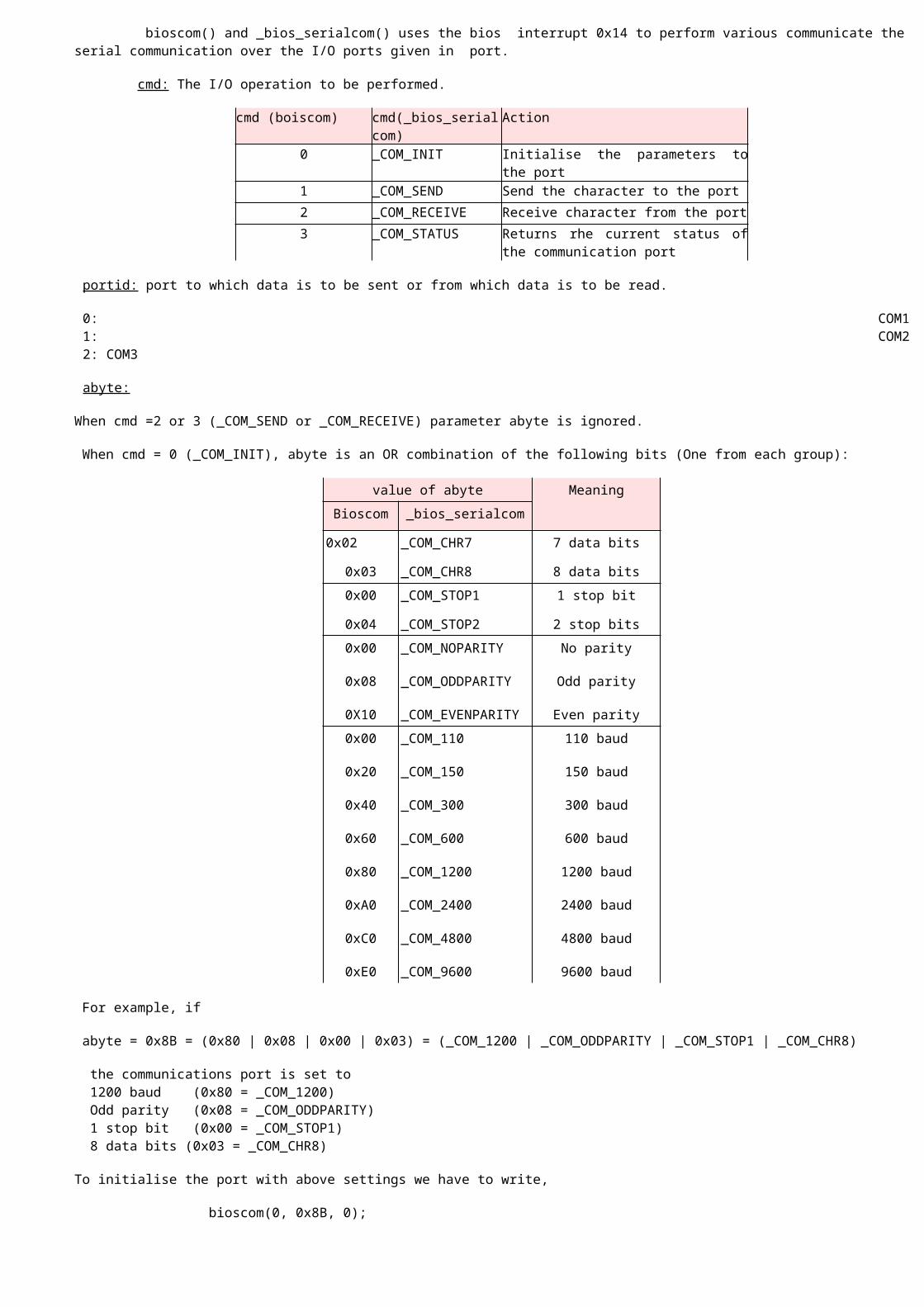
Industry Standard Architecture
One 8-bit and five 16-bit ISA slots on a motherboardYear created 1981; 34 years agoCreated by IBM
Superseded by PCI (1993)Width in bits 8 or 16
Number of devices Up to 6 devicesStyle Parallel
Hotplugging interface noExternal interface no
Fire Wire
FireWire is Apple Computer's version of a standard, IEEE 1394, High Performance Serial Bus, for connecting devices to your personal computer. FireWire provides a single plug-and-socket connection on which up to 63 devices can be attached with data transfer speeds up to 400 Mbps (megabits per second).
IEEE 1394 is an interface standard for a serial bus for high-speed communications and isochronous real-time data transfer. It was developed in the late 1980s and early 1990s by Apple, who called it FireWire. The 1394 interface is comparable to USB though USB has more market share.[1] Apple first included FireWire in some of its 1999 Macintosh models, and most Apple Macintosh computers manufactured in the years 2000 - 2011 included FireWire ports. However, in 2011 Apple began replacing FireWire with the Thunderbolt interface and, as of 2014, FireWire has been replaced by Thunderbolt on new Macs.[2] The 1394 interface is also known by the brand i.LINK (Sony), and Lynx (Texas Instruments). IEEE 1394 replaced parallel SCSI in many applications, because of lower implementation costs and a simplified, more adaptable cabling system. The 1394 standard also defines a backplane interface, though this is not as widely used.
IEEE 1394 was the High-Definition Audio-Video Network Alliance (HANA) standard connection interface for A/V (audio/visual) component communication and control
4-conductor (left) and 6-conductor (right) FireWire 400 alpha connectors
Unit-11USB bus Introduction
USB, short for Universal Serial Bus, is an industry standard developed in the mid-1990s that defines the cables, connectors and communications protocols used in a bus for connection, communication, and power supply between computers and electronic devices.
USB was designed to standardize the connection of computer peripherals (including keyboards, pointing devices, digital cameras, printers, portable media players, disk drives and network adapters) to personal computers, both to communicate and to supply electric power. It has become commonplace on other devices, such as smartphones, PDAs and video game consoles.[3] USB has effectively replaced a variety of earlier interfaces, such as serial and parallel ports, as well as separate power chargers for portable devices.
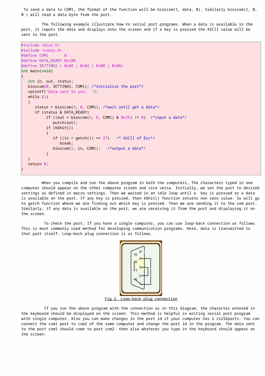
Certified USB logo
Type Bus
Production history
Designer Compaq, DEC, IBM, Intel, Microsoft, NEC and Nortel
Designed January 1996; 19 years ago
Manufacturer Compaq, DEC, IBM, Intel, Microsoft, NEC and Nortel
Produced Since 1997
SupersededSerial port, parallel port, game port, Apple Desktop Bus, and PS/2 connector
General specifications
Length 2–5 m (6 ft 7 in–16 ft 5 in) (by category)
Width12 mm (A-plug),[1] 8.45 mm (B-plug); 7 mm (mini/micro-USB); 8.25 mm (C-plug)
Height
4.5 mm (A-plug),[1] 7.78 mm (B-plug, pre-v3.0); 1.5–3 mm (mini/micro-USB); 2.4 mm (C-plug)
Hot pluggable Yes
External Yes
CableFour wires plus shield (pre-3.0); nine wires plus shield (USB 3.0)
Pins
4: one power supply, two data, one ground (pre-3.0);
5: (pre-3.0 micro-USB)
9: (USB 3.0);
11: (powered USB 3.0);
24: (USB type-C cable)
Connector Unique
Electrical
Signal 5 V DC
Max. voltage
5.00±0.25 V (pre-3.0)
5.00+0.25−0.55 V (USB 3.0)
20.00 V (USB-PD)
Max. current
0.5 A (USB 2.0)
0.9 A (USB 3.0 & 3.1)
1.5 A (USB BC 1.2)
3 A (USB Type-C)
Up to 5 A (USB-PD)
Data
Data signal Packet data, defined by specifications
Width One bit
Bitrate 1.5, 12, 480, 5,000, 10,000 Mbit/s (depending on
mode)
Max. devices 127Protocol Serial
Pin out
The standard-A USB plug (left) and standard-B plug (right)
Pin 1 VCC (+5 V, red wire)
Pin 2 Data− (white wire)
Pin 3 Data+ (green wire)
Pin 4 Ground (black wire)
USB is a Bus
Picture a setup of plugged-in hubs and devices such as that on the right. What we need to remember is that, at any point in time, only the host OR one device can be transmitting at a time.
When the host is transmitting a packet of data, it is sent to every device connected to an enabled port. It travels downwards via each hub in the chain which resynchronises the data transitions as it relays it. Only one device, the addressed one, actually accepts the data. (The others all receive it but the address is wrong for them.)
One device at a time is able to transmit to the host, in response to a direct request from the host. Each hub repeats any data it receives from a lower device in an upward only direction.
Downstream direction ports are only enabled once the device connected to them is addressed, except that one other port at a time can reset a device to address 0 and then set its address to a unique value.
Transceivers
At each end of the data link between host and device is a transceiver circuit. The transceivers are similar, differing mainly in the associated resistors.
A typical upstream end transceiver is shown to the right with high speed components omitted for clarity. By upstream, we mean the end nearer to the host. The upstream end has two 15K pull-down resistors.
Each line can be driven low individually, or a differential data signal can be applied. The maximum 'high' level is 3.3V.
The equivalent downstream end transceiver, as found in a device, is shown to the right.
When receiving, individual receivers on each line are able to detect single ended signals, so that the so-called Single Ended Zero (SE0) condition, where both lines are low, can be detected. There is also a differential receiver for reliable reception of data.
Not shown in these simplified drawings is the rise and fall time control on the differential transmitters. Low speed devices need longer rise and fall times, so a full speed / low speed hub must be able to switch between these rise and fall times.
Upstream End Transceiver
Downstream End Transceiver (Full Speed)
Speed Identification
At the device end of the link a 1.5 kohm resistor pulls one of the lines up to a 3.3V supply derived from VBUS.
This is on D- for a low speed device, and on D+ for a full speed device.
(A high speed device will initially present itself as a full speed device with the pull-up resistor on D+.)
The host can determine the required speed by observing which line is pulled high.
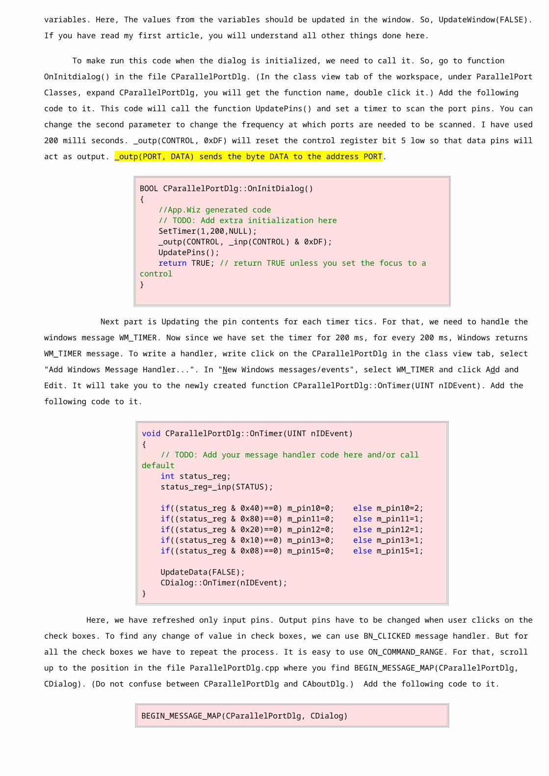
Line States
Given that there are just 2 data lines to use, it is surprising just how many different conditions are signaled using them:
Detached
When no device is plugged in, the host will see both data lines low, as its 15 kohm resistors are pulling each data line low.
Attached
When the device is plugged in to the host, the host will see either D+ or D- go to a '1' level, and will know that a device has been plugged in.
The '1' level will be on D- for a low speed device, and D+ for a full (or high) speed device.
Idle
The state of the data lines when the pulled up line is high, and the other line is low, is called the idle state. This is the state of the lines before and after a packet is sent.
J, K and SEO States
To make it easier to talk about the states of the data lines, some special terminology is used. The 'J State' is the same polarity as the idle state (the line with the pull-up resistor is high, and the other line is low), but is being driven to that state by either host or device.
The K state is just the opposite polarity to the J state.
The Single Ended Zero (SE0) is when both lines are being pulled low.
The J and K terms are used because for Full Speed and Low Speed links they are actually of opposite polarity.
Bus State Levels
Differential '1' D+ high, D- low
Differential '0' D- high, D+ low
Single Ended Zero (SE0) D+ and D- low
Single Ended One (SE1) D+ and D- high
Data J State:Low-speedFull-speed
Differential '0' Differential '1'
Data K State:Low-speedFull-speed
Differential '1' Differential '0'
Idle State:Low-speedFull-speed
D- high, D+- lowD+ high, D- low
Resume State Data K state
Start of Packet (SOP)Data lines switch from idle to K state
End of Packet (EOP)SE0 for 2 bit times followed by J state for 1 bit time
Disconnect SE0 for >= 2us
Connect Idle for 2.5us
Reset SE0 for >= 2.5 us
Bus States
This table has been simplified from the original in the USB specification. Please read the original table for complete information.
Single Ended One (SE1)
This is the illegal condition where both lines are high. It should never occur on a properly functioning link.
Reset
When the host wants to start communicating with a device it will start by applying a 'Reset' condition which sets the device to its default unconfigured state.
The Reset condition involves the host pulling down both data lines to low levels (SE0) for at least 10 ms. The device may recognise the reset condition after 2.5 us.
This 'Reset' should not be confused with a micro-controller power-on type reset. It is a USB protocol reset to ensure that the device USB signaling starts from a known state.
EOP signal
The End of Packet (EOP) is an SE0 state for 2 bit times, followed by a J state for 1 bit time.
Suspend
One of the features of USB which is an essential part of today's emphasis of 'green' products is its ability to power down an unused device. It does this by suspending the device, which is achieved by not sending anything to the device for 3 ms.
Normally a SOF packet (at full speed) or a Keep Alive signal (at low speed) is sent by the host every 1 ms, and this is what keeps the device awake.
A suspended device may draw no more than 0.5 mA from Vbus.
A suspended device must recognise the resume signal, and also the reset signal.
If a device is configured for high power (up to 500 mA), and has its remote wakeup feature enabled, it is allowed to draw up to 2.5mA during suspend.
Resume
When the host wants to wake the device up after a suspend, it does so by reversing the polarity of the signal on the data lines for at least 20ms. The signal is completed with a low speed end of packet signal.
It is also possible for a device with its remote wakeup feature set, to initiate a resume itself. It must have been in the idle state for at least 5ms, and must apply the wakeup K condition for between 1 and 15 ms. The host takes over the driving of the resume signal within 1 ms.
Keep Alive Signal
This is represented by a Low speed EOP. It is sent at least once every millisecond on a low speed link, in order to keep the device from suspending.
Packets
The packet could be thought of as the smallest element of data transmission. Each packet conveys an integral number of bytes at the current transmission rate. Before and after the packet, the bus is in the idle state.
You need not be concerned with the detail of syncs, bit stuffing, and End Of Packet conditions, unless you are designing at the silicon level, as the Serial Interface Engine (SIE) will deal with the details for you. You should just be aware that the SIE can recognise the start and end of a packet, and that the packet contains a whole number of bytes.
In spite of this packets often expect fields of data to cross byte boundaries. The important rule to remember is that all usb fields are transmitted least significant bit first. So if, for example, a field is defined by 2 successive bytes, the first byte will be the least significant, and the second byte transmitted will be the most significant.
Serial Interface Engine (SIE)
The complexities and speed of the USB protocol are such that it is not practical to expect a general purpose micro-controller to be able to implement the protocol using an instruction-driven basis. Dedicated hardware is required to deal with the time-critical portions of the specification, and the circuitry grouping which performs this function is referred to as the Serial Interface Engine (SIE).
Data Fields are Transmitted Least Significant Bit First
The first time when you need to know this is when you are defining 'descriptors' in your firmware code. Many of these values are word sized and you need to add the bytes in the low byte, high byte order.
A packet starts with a sync pattern to allow the receiver bit clock to synchronise with the data. It is followed, by the data bytes of the packet, and concluded with an End of Packet (EOP) signal. The data is actually NRZI encoded, and in order to ensure sufficiently frequent transitions,
Idle SYNC DATA BYTES EOP Idle
A Single Packet
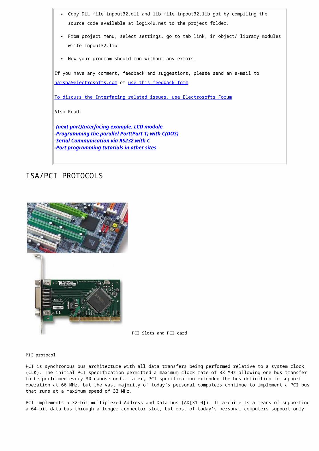
a zero is inserted after 6 successive 1's (this is known as bit stuffing).
Before we continue, some definitions...
Endpoints
Each USB device has a number of endpoints. Each endpoint is a source or sink of data. A device can have up to 16 OUT and 16 IN endpoints.
OUT always means from host to device.
IN always means from device to host.
Endpoint 0 is a special case which is a combination of endpoint 0 OUT and endpoint 0 IN, and is used for controlling the device.
Pipe
A logical data connection between the host and a particular endpoint, in which we ignore the lower level mechanisms for actually achieving the data transfers.
Transactions
Simple transfers of data called 'Transactions' are built up using packets.
Packet Formats
The first byte in every packet is a Packet Identifier (PID) byte. This byte needs to be recognized quickly by the SIE and so is not included in any CRC checks. It therefore has its own validity check. The PID itself is 4 bits long, and the 4 bits are repeated in an complemented form.
lsb msb
PID0
PID1
PID2
PID3
\PID0
\PID1
\PID2
\PID3
The PID is shown here in the order of transmission; lsb first.
Cyclic Redundancy Code (CRC)
A CRC is a value calculated from a number of data bytes to form a unique value which is transmitted along with the data bytes, and then used to validate the correct reception of the data.
USB uses two different CRCs, one 5 bits long (CRC5) and one 16 bits long (CRC16).
See the USB specification for details of the algorithms used.
There are 17 different PID values defined. This includes one reserved value, and one value which has been used twice with different meanings for two different situations.
PID Type PID Name PID<3:0>*
Token OUT 0001b
IN 1001b
Notice that the first 2 bits of a token which are transmitted, determine which of the 4 groups it falls into. This is why SOF is officially considered to be a token PID.
SOF 0101b
SETUP 1101b
Data
DATA0 0011b
DATA1 1011b
DATA2 0111b
MDATA 1111b
Handshake
ACK 0010b
NAK 1010b
STALL 1110b
NYET 0110b
Special
PRE 1100b
ERR 1100b
SPLIT 1000b
PING 0100b
Reserved 0000b
* Bits are transmitted lsb first
There are four different packet formats based on which PID the packet starts with.
Token PacketSync PID ADDR ENDP CRC5 EOP
8 bits 7 bits 4 bits 5 bits
Used for SETUP, OUT and IN packets. They are always the first packet in a transaction, identifying the targeted endpoint, and the purpose of the transaction.
The SOF packet is also defined as a Token packet, but has a slightly different format and purpose, which is described below.
The token packet contains two addressing elements:
Address (7 bits)
This device address can address up to 127 devices. Address 0 is reserved for a device which has not yet had its address set.
Endpoint number (4 bits)
There can be up to 16 possible endpoints in a device in each direction. The direction is implicit in the PID. OUT and SETUP PIDs will refer to the OUT endpoint, and an IN PID will refer to the IN endpoint.
Data PacketSync PID DATA CRC16 EOP
8 bits(0-1024)x 8 bits
16 bits
Used for DATA0, DATA1, DATA2 and MDATA packets. If a transaction has a data stage this is the packet format used.
DATA0 and DATA1 PIDs are used in Low and Full speed links as part of an error-checking system. When used, all data packets on a particular endpoint use an alternating DATA0 / DATA1 so that the endpoint knows if a received packet is the one it is expecting. If it is not it will still acknowledge (ACK) the packet as it is correctly received, but will then discard the data, assuming that it has been re-sent because the host missed seeing the ACK the first time it sent the data packet.
DATA2 and MDATA are only used for high speed links.
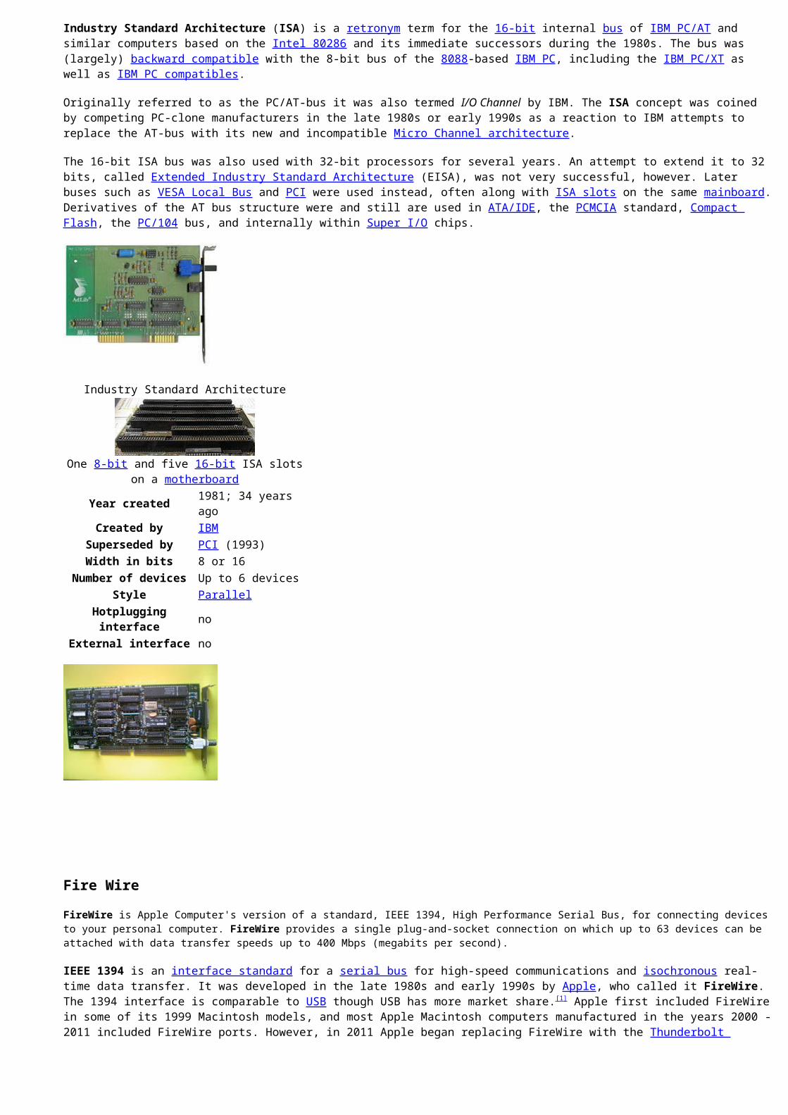
Handshake PacketSync PID EOP
8 bits
Used for ACK, NAK, STALL and NYET packets. This is the packet format used in the status stage of a transaction, when required.
ACK
Receiver acknowledges receiving error free packet.
NAK
Receiving device cannot accept data or transmitting device cannot send data.
STALL
Endpoint is halted, or control pipe request is not supported.
NYET
No response yet from receiver (high speed only)
SOF Packet
Sync PIDFrame
No.CRC5 EOP
8 bits 11 bits 5 bits
The Start of Frame packet is sent every 1 ms on full speed links. The frame is used as a time frame in which to schedule the data transfers which are required. For example, an isochronous endpoint will be assigned one transfer per frame.
Frames
On a low speed link, to preserve bandwidth, a Keep Alive signal is sent every millisecond, instead of a Start of Frame packet. In fact Keep Alives may be sent by a hub on a low speed link whenever the hub sees a full speed token packet.
At high speed the 1 ms frame is divided into 8 microframes of 125 us. A SOF is sent at the start of each of these 8 microframes, each having the same frame number, which then increments every 1 ms frame.
Transactions
A successful transaction is a sequence of three packets which performs a simple but secure transfer of data.
For IN and OUT transactions used for isochronous transfers, there are only 2 packets; the handshake packet on the end is omitted. This is because error-checking is not required.
There are three types of transaction. In each of the illustrations below, the packets from the host are shaded, and the packets from the device are not.
OUT Transaction
A successful OUT transaction comprises two or three sequential packets. If it were being used in an Isochronous Transfer there would not be a handshake packet from the device.
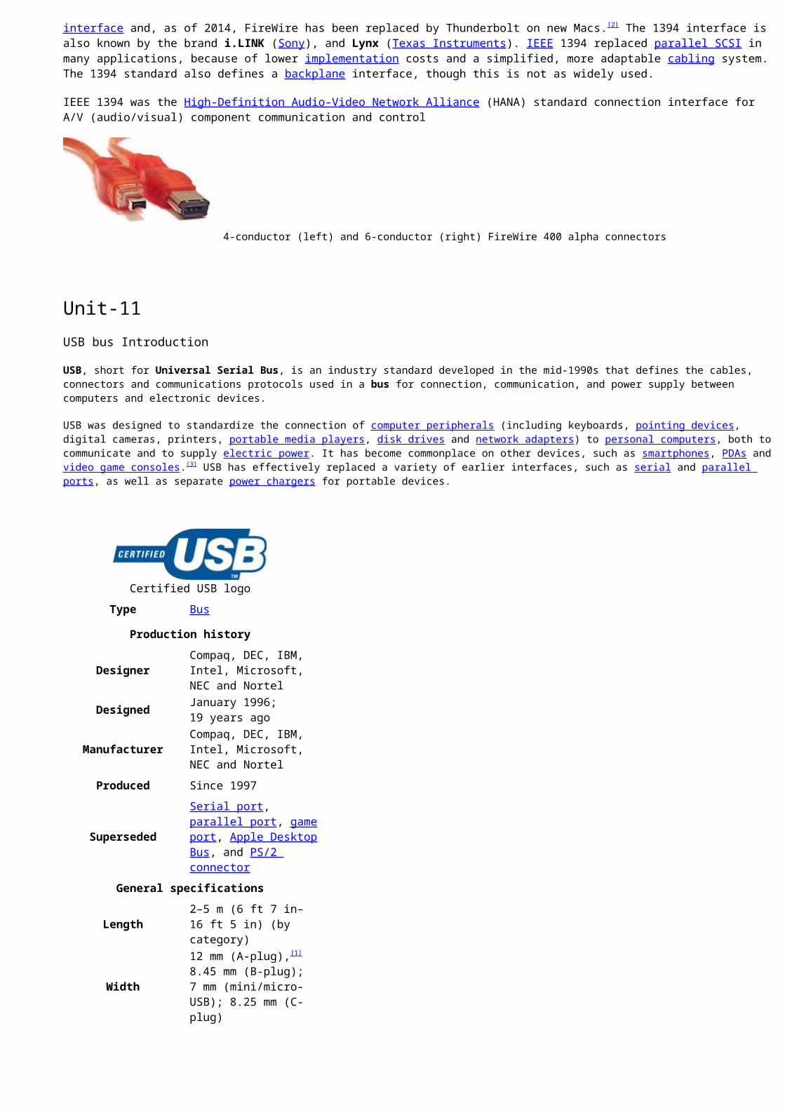
On a low or full speed link, the PID shown as DATAx will be either a DATA0 or a DATA1. An alternating DATA0/DATA1 is used as a part of the error control protocol to (or from) a particular endpoint.
IN Transaction
A successful IN transaction comprises two or three sequential packets. If it were being used in an Isochronous Transfer there would not be a handshake packet from the host.
Here again, the DATAx is either a DATA0 or a DATA1.
SETUP Transaction
A successful SETUP transaction comprises three sequential packets. This is similar to an OUT transaction, but the data payload is exactly 8 bytes long, and the SETUP PID in the token packet informs the device that this is the first transaction in a Control Transfer (see below).
As will be seen below, the SETUP transaction always uses a DATA0 to start the data packet.
Data Flow Types
There are four different ways to transfer data on a USB bus. Each has its own purposes and characteristics. Each one is built up using one or more transaction type.
Data Flow Type Description
Control TransferMandatory using Endpoint 0 OUT and Endpoint 0 IN.
Bulk TransferError-free high volume throughput when bandwidth available.
Interrupt TransferRegular Opportunity for status updates, etc.Error-free Low throughput
Isochronous Transfer
Guaranteed fixed bandwidth.Not error-checked.
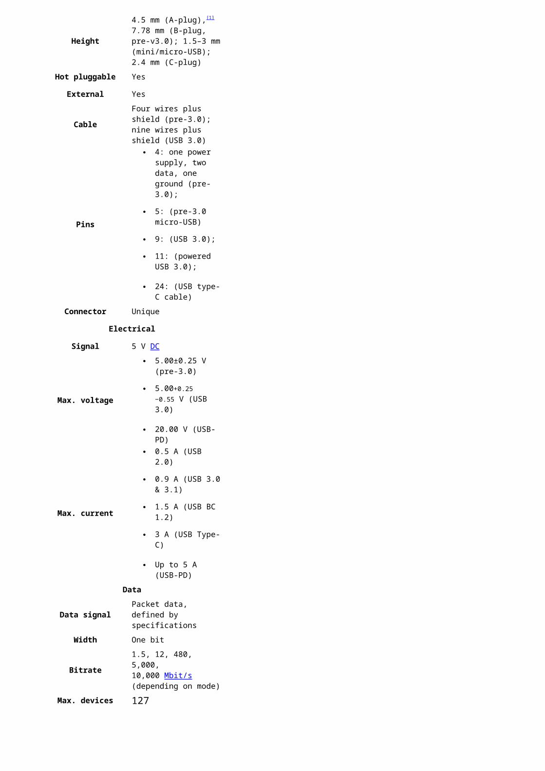
Bulk Transfers
Bulk transfers are designed to transfer large amounts of data with error-free delivery, but with no guarantee of bandwidth. The host will schedule bulk transfers after the other transfer types have been allocated.
If an OUT endpoint is defined as using Bulk transfers, then the host will transfer data to it using OUT transactions.
If an IN endpoint is defined as using Bulk transfers, then the host will transfer data from it using IN transactions.
The max packet size is 8, 16, 32 or 64 at full Speed and 512 for high speed. Bulk transfers are not allowed at low speed.
Use Bulk transfers when you have a lot of data to shift, as fast as possible, but where you would not have a large problem if there is a delay caused by insufficient bandwidth.
Example Bulk Transfer
The diagrams to the right illustrate the possible flow of events in the face of errors.
Error Control - IN
If the IN token packet is not recognised, the device will not respond at all. Otherwise, if it has data to send it will send it in a DATA0 or DATA1 packet; If it is not ready to send data it will send a NAK packet. If the endpoint is currently 'halted' then it will respond with a STALL packet.
In the case of DATA0/1 being sent, the host will acknowledge with an ACK, unless the data is not validly received, in which case it does not send an ACK. (Note: the host never sends NAK!)
Error Control - OUT
If the OUT token packet is not recognised, the device will not respond at all. It will then ignore the DATAx packet because it does not know that it has been addressed.
If the OUT token is recognised but the DATAx packet is not recognised, then the device will not respond.
If the data is received but the device can't accept it at this time, it will send a NAK, and if the endpoint is currently halted, it will send a STALL.
BULK Transfer Error Control Flow
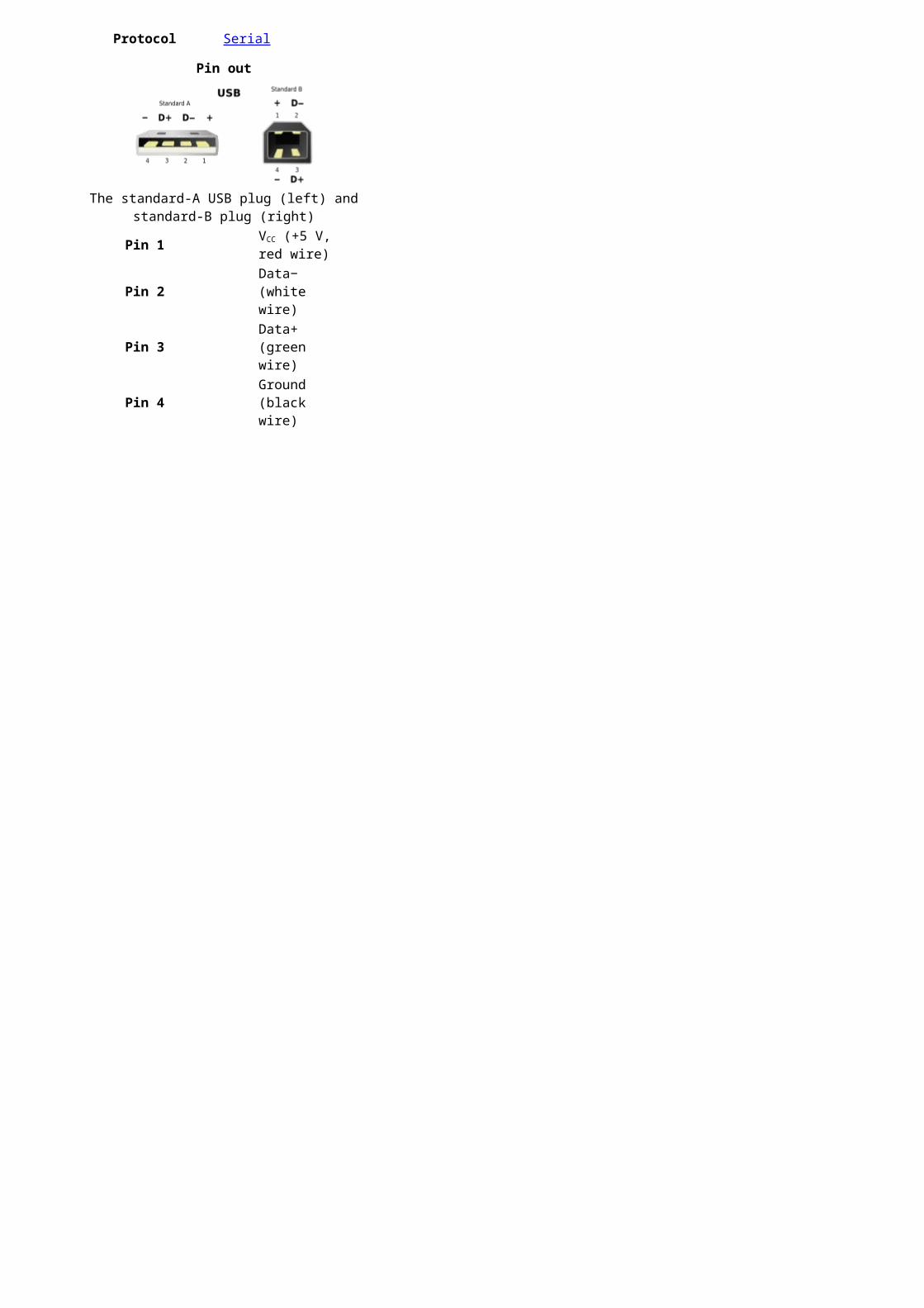
Interrupt Transfers
Interrupt transfers have nothing to do with interrupts. The name is chosen because they are used for the sort of purpose where an interrupt would have been used in earlier connection types.
Interrupt transfers are regularly scheduled IN or OUT transactions, although the IN direction is the more common usage.
Typically the host will only fetch one packet, at an interval specified in the endpoint descriptor (see below). The host guarantees to perform the IN transaction at least that often, but it may actually do it more frequently.
Interrupt packets can have any size from 1 to 8 bytes at low speed, from 1 to 64 at full speed or up to 1024 bytes at high speed.
Use an interrupt transfer when you need to be regularly kept up to date of any changes of status in a device. Examples of their use are for a mouse or a keyboard.
Error control is very similar to that for bulk transfers.
Example Interrupt Transfer
Error Control Flow
Isochronous Transfers
Isochronous transfers have a guaranteed bandwidth, but error-free delivery is not guaranteed.
The main purpose of isochronous transfers is applications such as audio data transfer, where it is important to maintain the data flow, but not so important if some data gets missed or corrupted.
An isochronous transfer uses either an IN transaction or an OUT transaction depending on the type of endpoint. The special feature of these transactions is that there is no handshake packet at the end.
An isochronous packet may contain up to 1023 bytes at full speed, or up to 1024 at high speed. Isochronous transfers are not allowed at low speed.
Example Isochronous Transfer
Error Control Flow
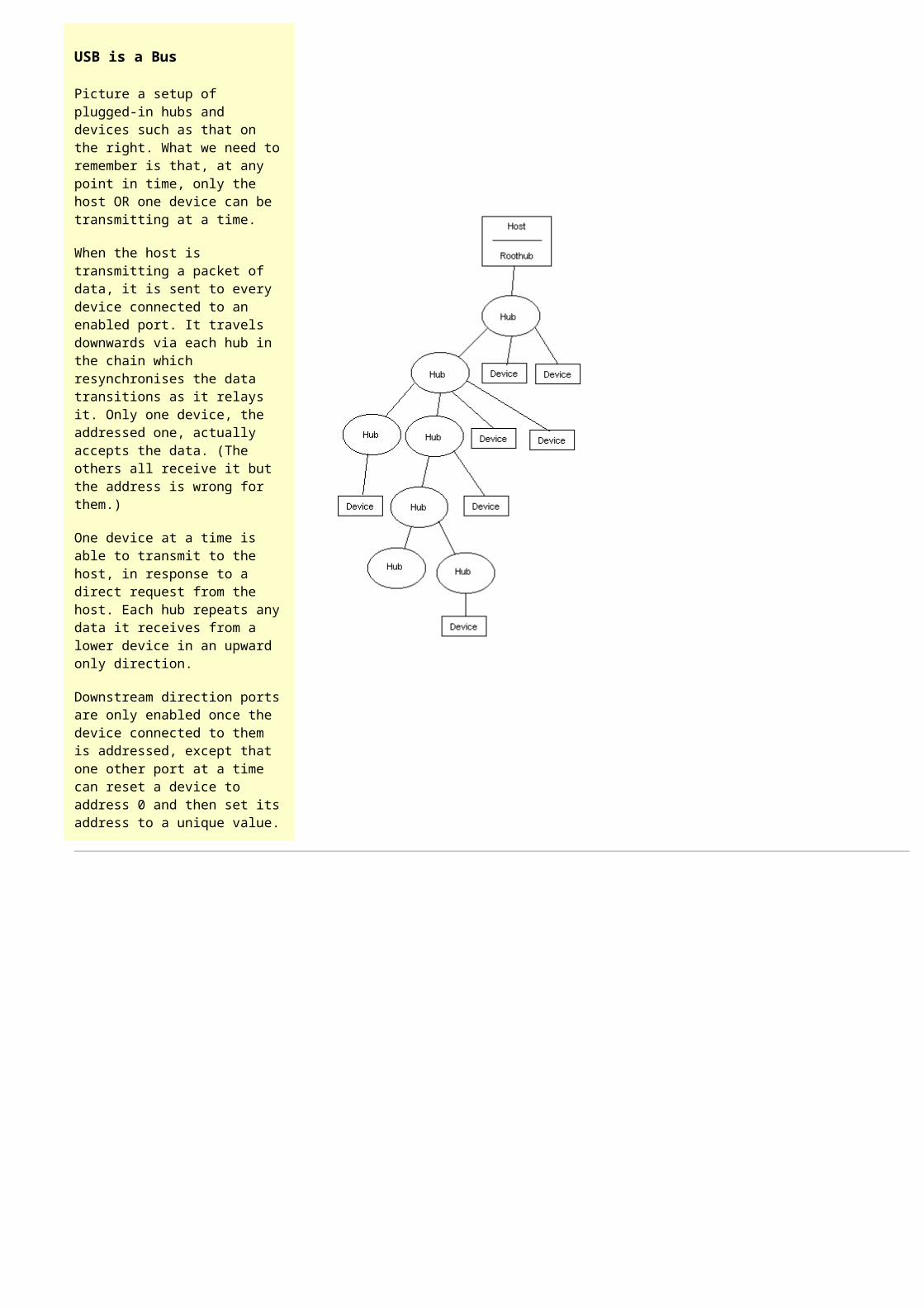
Control Transfer
This is a bi-directional transfer which uses both an IN and an OUT endpoint. Each control transfer is made up of from 2 to several transactions.
It is divided into three stages.
The SETUP stage carries 8 bytes called the Setup packet. This defines the request, and specifies whether and how much data should be transferred in the DATA stage.
The DATA stage is optional. If present, it always starts with a transaction containing a DATA1. The type of transaction then alternates between DATA0 and DATA1 until all the required data has been transferred.
The STATUS stage is a transaction containing a zero-length DATA1 packet. If the DATA stage was IN then the STATUS stage is OUT, and vice versa.
Control transfers are used for initial configuration of the device by the host, using Endpoint 0 OUT and Endpoint 0 IN, which are reserved for this purpose. They may be used (on the same endpoints) after configuration as part of the device-specific control protocol, if required.
The max packet size for the data stage is 8 bytes at low speed, 8, 16, 32 or 64 at full Speed and 64 for high speed.
Example Control Read
Error Control FlowSETUP STAGE
Notice that it is not permitted for a device to respond to a SETUP with a NAK or a STALL.
DATA STAGE
(same as for bulk transfer)
STATUS STAGE
(same as for bulk transfer)
SummaryWe have examined 4 different types of data transfer, each of which uses different combinations of packets.
We have seen Control Transfers which every device uses to implement a Standard set of requests. And we have seen three other data transfer types, which a device might use depending on its purpose.
Coming up...
Next we will examine the standard set of requests which every USB device has to implement.
Forward
Copyright © 2006-2008 MQP Electronics Ltd
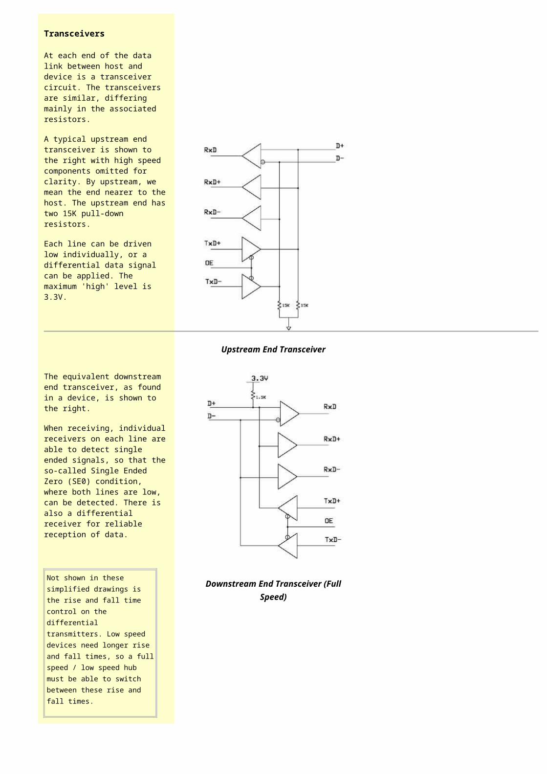
ADVERTISEMENT
Packet-Master USB Bus Analysers and Generators from MQP Electronics
Special Offer
PIC 18 microcontroller usb interface
PIC microcontrollers are a family of specialized microcontroller chips produced by Microchip Technology in Chandler, Arizona. The acronym PIC stands for "peripheral interface controller," although that term is rarely used nowadays.
CAN bus
The CAN Bus Protocol
This is a brief introduction to the CAN bus protocol. When people talk about “CAN” without further detailing what standards they are talking about, they usually mean the data link layer protocol defined by ISO 11898-1 and the physical layer defined by ISO 11898-2. In reality, there are many standards to choose from.
Controller Area Network (CAN) interface in embedded systems:
History:
CAN or Controller Area Network or CAN-bus is an ISO standard computer network protocol and bus standard, designed for microcontrollers and devices to communicate with each other without a host computer. Designed earlier for industrial networking but recently more adopted to automotive applications, CAN have gained widespread popularity for embedded control in the areas like industrial automation, automotives, mobile machines, medical, military and other harsh environment network applications.
Development of the CAN-bus started originally in 1983 at Robert Bosch GmbH. The protocol was officially released in 1986. and the first CAN controller chips, produced by Intel and Philips, introduced in the market in the year of 1987.
Introduction:
The CAN is a "broadcast" type of bus. That means there is no explicit address in the messages. All the nodes in the network are able to pick-up or receive all transmissions. There is no way to send a message to just a specific node. To be more specific, the messages transmitted from any node on a CAN bus does not contain addresses of either the transmitting node, or of any intended receiving node. Instead, an identifier that is unique throughout the network is used to label the content of the message. Each message carries a numeric value, which controls its priority on the bus, and may also serve as an identification of the contents of the message. And each of the receiving nodes performs an acceptance test or provides local filtering on the identifier to determine whether the message, and thus its content, is relevant to that particular node or not, so that each node may react only on the intended messages. If the message is relevant, it will be processed; otherwise it is ignored.
How do they communicate?If the bus is free, any node may begin to transmit. But what will happen in situations where two or more nodes attempt to transmit message (to the CAN bus) at the same time. The identifier field, which is unique throughout the network helps to determine the priority of the message. A "non-destructive arbitration technique" is used to accomplish this, to ensure that the messages are sent in order of priority and that no messages are lost. The lower the numerical value of the identifier, the higher the priority. That means the message with identifier having more dominant bits (i.e. bit 0) will overwrite other nodes' less dominant identifier so that eventually (after the arbitration on the ID) only the dominant message remains and is received by all nodes.As stated earlier, CAN do not use address-based format for communication, instead uses a message-based data format. Here the information is transferred from one location to another by sending a group of bytes at one time (depending on the order of priority). This makes CAN ideally suited in applications requiring a large number of short messages (e.g.: transmission of temperature and rpm information). by more than one location and system-wide data consistency is mandatory. (The traditional networks such as USB or Ethernet are used to send large blocks of data, point-to-point from node A to node B under the supervision of a central bus master).Let us now try to understand how these nodes are interconnected physically, by pointing out some examples. A modern automobile system will have many electronic control units for various subsystems (fig1-a). Typically the biggest processor will be the engine control unit (or the host processor). The CAN standard even facilitates the subsystem to control actuators or receive signals from sensors. A CAN message never reaches these devices directly, but instead a host-processor and a CAN Controller (with a CAN transciever) is needed between these devices and the bus. (In some cases, the network need not have a controller node; each node can easily be connected to the main bus directly.)The CAN Controller stores received bits (one by one) from the bus until an entire message block is available, that can then be fetched by the host processor (usually after the CAN Controller has triggered an interrupt). The Can transciever adapts signal levels from the bus, to levels that the CAN Controller expects
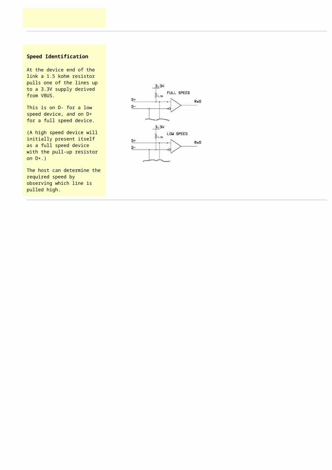
and also provides a protective circuitry for the CAN Controller. The host-processor decides what the received messages mean, and which messages it wants to transmit itself.
Fig 1-aIt is likely that the more rapidly changing parameters need to be transmitted more frequently and, therefore, must be given a higher priority. How this high-priority is achieved? As we know, the priority of a CAN message is determined by the numerical value of its identifier. The numerical value of each message identifier (and thus the priority of the message) is assigned during the initial phase of system design. To determine the priority of messages (while communication), CAN uses the established method known as CSMA/CD with the enhanced capability of non-destructive bit-wise arbitration to provide collision resolution and to exploit the maximum available capacity of the bus. "Carrier Sense" describes the fact that a transmitter listens for a carrier wave before trying to send. That is, it tries to detect the presence of an encoded signal from another station before attempting to transmit. If a carrier is sensed, the node waits for the transmission in progress to finish before initiating its own transmission. "Multiple Access" describes the fact that multiple nodes send and receive on the same medium. All other nodes using the medium generally receive transmissions by one node. "Collision Detection" (CD) means that collisions are resolved through a bit-wise arbitration, based on a preprogrammed priority of each message in the identifier field of a message.
Fig 1-b
Let us now try to understand how the term "priority" becomes more important in the network. Each node can have one or more function. Different nodes may transmit messages at different times (Depends how the system is configured) based on the function(s) of each node. For example:1) Only when a system failure (communication failure) occurs.2) Continually, such as when it is monitoring the temperature.3) A node may take action or transmit a message only when instructed by another node, such as when a fan controller is instructed to turn a fan on when the temperature-monitoring node has detected an elevated temperature.Note: When one node transmits the message, sometimes many nodes may accept the message and act on it (which is not a usual case). For example, a temperature-sensing node may send out temperature data that are accepted & acted on only by a temperature display node. But if the temperature sensor detects an over-temperature situation, then many nodes might act on the information.CAN use "Non Return to Zero" (NRZ) encoding (with "bit-stuffing") for data communication on a "differential two wire bus". The two-wire bus is usually a twisted pair (shielded or unshielded). Flat pair (telephone type) cable also performs well but generates more noise itself, and may be more susceptible to external sources of noise.Main Features:
a) A two-wire, half duplex, high-speed network system mainly suited for high-speed applications using "short messages". (The message is transmitted serially onto the bus, one bit after another in a specified format).b) The CAN bus offers a high-speed communication rate up to 1 M bits / sec, for up to 40 feet, thus facilitating real-time control. (Increasing the distance may decrease the bit-rate).c) With the message-based format and the error-containment followed, it's possible to add nodes to the bus without reprogramming the other nodes to recognize the addition or changing the existing hardware. This can be done even while the system is in operation. The new node will start receiving messages from the network immediately. This is called "hot-plugging"d) another useful feature built into the CAN protocol is the ability of a node to request information from other nodes. This is called a remote transmit request, or RTR.e) The use of NRZ encoding ensures compact messages with a minimum number of transitions and high resilience to external disturbance.f) CAN protocol can link up to 2032 devices (assuming one node with one identifier) on a single network. But accounting to the practical limitations of the hardware (transceivers), it may only link up to 110 nodes on a single network. g) Has an extensive and unique error checking mechanisms.h) Has High immunity to Electromagnetic Interference. Has the ability to self-diagnose & repair data errors.i) Non-destructive bit-wise arbitration provides bus allocation on the basis of need, and delivers efficiency benefits that can not be gained from either fixed time schedule allocation (e.g. Token ring) or destructive bus allocation (e.g. Ethernet.)j) Fault confinement is a major advantage of CAN. Faulty nodes are automatically dropped from the bus. This helps to prevent any single node from bringing
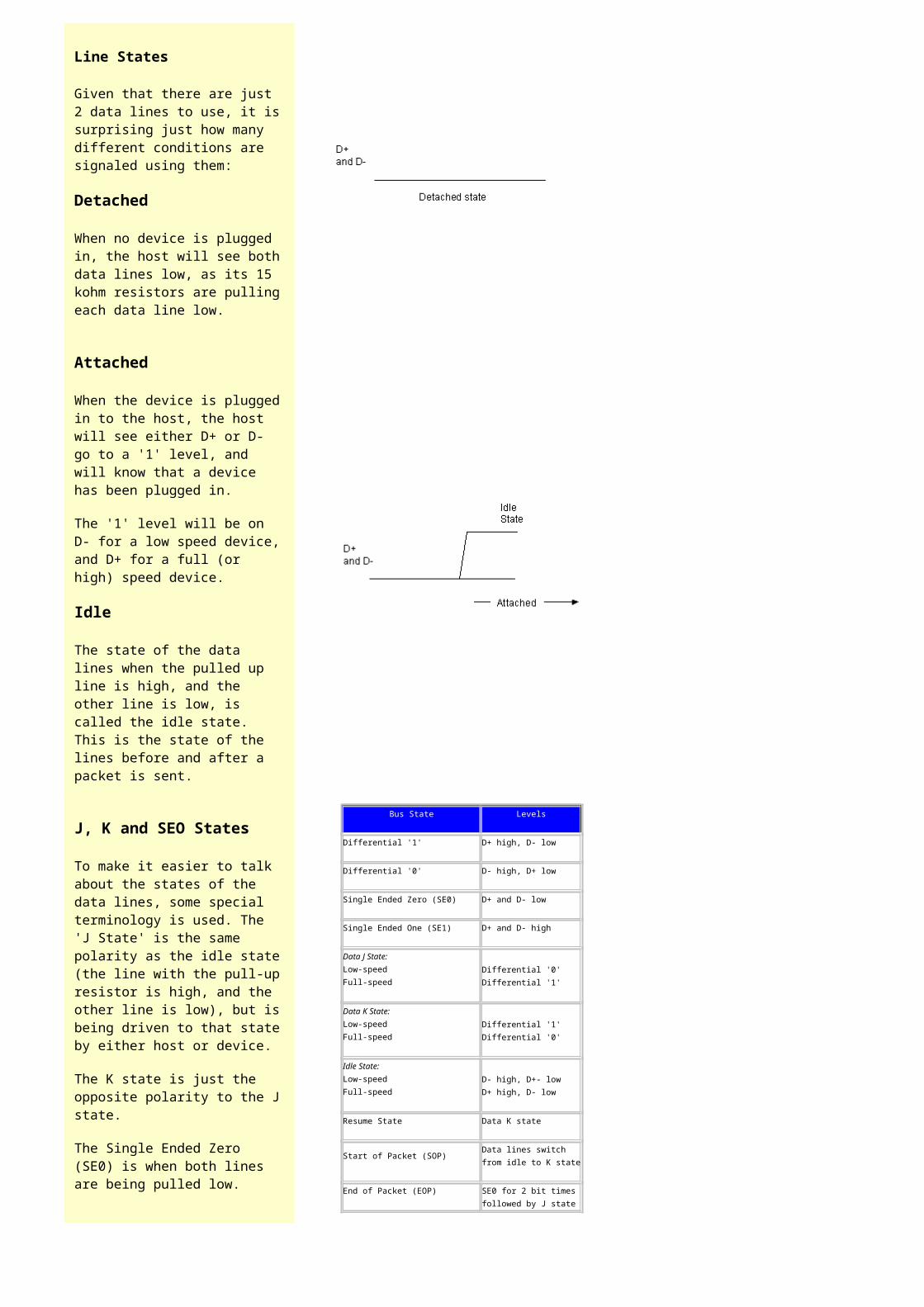
the entire network down, and thus ensures that bandwidth is always available for critical message transmission.k) The use of differential signaling (a method of transmitting information electrically by means of two complementary signals sent on two separate wires) gives resistance to EMI & tolerance of ground offsets. l) CAN is able to operate in extremely harsh environments. Communication can still continue (but with reduced signal to noise ratio) even if:1. Either of the two wires in the bus is broken2. Either wire is shorted to ground3. Either wire is shorted to power supply.
CAN protocol Layers & message Frames:
Like any network applications, Can also follows layered approach to the system implementation. It conforms to the Open Systems Interconnection (OSI) model that is defined in terms of layers. The ISO 11898 (For CAN) architecture defines the lowest two layers of the seven layers OSI/ISO model as the data-link layer and physical layer. The rest of the layers (called Higher Layers) are left to be implemented by the system software developers (used to adapt and optimize the protocol on multiple media like twisted pair. Single wire, optical, RF or IR). The Higher Level Protocols (HLP) is used to implement the upper five layers of the OSI in CAN.
CAN use a specific message frame format for receiving and transmitting the data. The two types of frame format available are:
a) Standard CAN protocol or Base frame formatb) Extended Can or Extended frame format
The following figure (Fig 2) illustrates the standard CAN frame format, which consists of seven different bit-fields.
a) A Start of Frame (SOF) field - indicates the beginning of a message frame.b) An Arbitration field, containing a message identifier and the Remote Transmission Request (RTR) bit. The RTR bit is used to discriminate between a transmitted Data Frame and a request for data from a remote node. c) A Control Field containing six bits in which two reserved bits (r0 and r1) and a four bit Data Length Code (DLC). The DLC indicates the number of bytes in the Data Field that follows. d) A Data Field, containing from zero to eight bytes.e) The CRC field, containing a fifteen-bit cyclic redundancy check-code and a recessive delimiter bit.f) The Acknowledge field, consisting of two bits. The first one is a Slot bit which is transmitted as recessive, but is subsequently over written by dominant bits transmitted from any node that successfully receives the transmitted message. The second bit is a recessive delimiter bit.g) The End of Frame field, consisting of seven recessive bits.
An Intermission field consisting of three recessive bits is then added after the EOF field. Then the bus is recognized to be free.
(Fig 2)
The Extended Frame format provides the Arbitration field with two identifier bit fields. The first (the base ID) is eleven (11) bits long and the second field (the ID extension) is eighteen (18) bits long, to give a total length of twenty nine (29) bits. The distinction between the two formats is made using an Identifier Extension (IDE) bit. A Substitute Remote Request (SRR) bit is also included in the Arbitration Field.
Error detection & correction:
This mechanism is used for detecting errors in messages appearing on the CAN bus, so that the transmitter can retransmit message. The CAN protocol defines five different ways of detecting errors. Two of these works at the bit level, and the other three at the message level. 1. Bit Monitoring. 2. Bit Stuffing. 3. Frame Check. 4. Acknowledgement Check. 5. Cyclic Redundancy Check
1. Each transmitter on the CAN bus monitors (i.e. reads back) the transmitted signal level. If the signal level read differs from the one transmitted, a Bit Error is signaled. Note that no bit error is raised during the arbitration process.
2. When five consecutive bits of the same level have been transmitted by a node, it will add a sixth bit of the opposite level to the outgoing bit stream. The receivers will remove this extra bit. This is done to avoid excessive DC components on the bus, but it also gives the receivers an extra opportunity to detect errors: if more than five consecutive bits of the same level occurs on the bus, a Stuff Error is signaled.
3. Some parts of the CAN message have a fixed format, i.e. the standard defines exactly what levels must occur and when. (Those parts are the CRC Delimiter, ACK Delimiter, End of Frame, and also the Intermission). If a CAN controller detects an invalid value in one of these fixed fields, a Frame Error is signaled.
4. All nodes on the bus that correctly receives a message (regardless of their being "interested" of its contents or not) are expected to send a dominant level in the so-called Acknowledgement Slot in the message. The transmitter will transmit a recessive level here. If the transmitter can't detect a dominant level in the ACK slot, an Acknowledgement Error is signaled.
5. Each message features a 15-bit Cyclic Redundancy Checksum and any node that detects a different CRC in the message than what it has calculated itself will produce a CRC Error.
Error confinement:
Error confinement is a technique, which is unique to CAN and provides a method for discriminating between temporary errors and permanent failures in the communication network. Temporary errors may be caused by, spurious external conditions, voltage spikes, etc. Permanent failures are likely to be caused by bad connections, faulty cables, defective transmitters or receivers, or long lasting external disturbances.
Let us now try to understand how this works.
Each node along the bus will be having two error counters namely the transmit error counter (TEC) and the receive error counter (REC), which are used to be incremented and/or decremented in accordance with the error detected. If a transmitting node detects a fault, then it will increments its TEC faster than the listening nodes increments its REC because there is a good chance that it is the transmitter who is at fault.A node usually operates in a state known as "Error Active" mode. In this condition a node is fully functional and both the error count registers contain counts of less than 127. When any one of the two error counters raises above 127, the node will enter a state known as "Error Passive". That means, it will not actively destroy the bus traffic when it detects an error. The node which is in error passive mode can still transmit and receive messages but are restricted in relation to how they flag any errors that they may detect. When the Transmit Error Counter rises above 255, the node will enter the Bus Off state, which means that the node doesn't participate in the bus traffic at all. But the communications between the other nodes can continue unhindered.
To be more specific, an "Error Active" node will transmit "Active Error Flags" when it detects errors, an "Error Passive" node will transmit "Passive Error Flags" when it detects errors and a node, which is in "Bus Off" state will not transmit "anything" on the bus at all. The transmit errors give 8 error points, and receive errors give 1 error point. Correctly transmitted and/or received messages cause the counter(s) to decrease. The other nodes will detect the error caused by the Error Flag (if they haven't already detected the original error) and take appropriate action, i.e. discard the current message.
Confused? Let us try to get slightly simplified.
Let's assume that whenever node-A (for example) on a bus tries to transmit a message, it fails (for whatever reason). Each time this happens, it increases its Transmit Error Counter by 8 and transmits an Active Error Flag. Then it will attempt to retransmit the message and suppose the same thing happens again. When the Transmit Error Counter rises above 127 (i.e. after 16 attempts), node A goes Error Passive. It will now transmit passive error flags on the bus. A Passive Error Flag comprises 6 recessive bits, and will not destroy other bus traffic - so the other nodes will not hear the node-A complaining about bus errors. However, A continues to increase its TEC. When it rises above 255, node-A finally stops and goes to "Bus Off" state. What does the other nodes think about node A? - For every active error flag that A transmitted, the other nodes will increase their Receive Error Counters by 1. By the time that A goes Bus Off, the other nodes will have a count in their Receive Error Counters that is well below the limit for Error Passive, i.e. 127. This count will decrease by one for every correctly received message. However, node A will stay bus off. Most CAN controllers will provide status bits and corresponding interrupts for two states: "Error Warning" (for one or both error counters are above 96) and "Bus Off".
Bit Timing and Synchronization:
The time for each bit in a CAN message frame is made up of four non-overlapping time segments as shown below.
The following points may be relevant as far as the "bit timing" is concerned.
1. Synchronization segment is used to synchronize the nodes on the bus. And it will always be of one quantum long. 2. One time quanta (which is also known as the system clock period) is the period of the local oscillator, multiplied by the value in the Baud Rate Pre-scaler (BRP) register in the CAN controller. 3. A bit edge is expected to take place during this synchronization segment when the data changes on the bus.4. Propagation segment is used to compensate for physical delay times within the network bus lines. And is programmable from one to eight time quanta long.5. Phase-segment1 is a buffer segment that can be lengthened during resynchronization to compensate for oscillator drift and positive phase differences between the oscillators of the transmitting and receiving nodes. And is also programmable from one to eight time quanta long.6. Phase-segment2 can be shortened during resynchronization to compensate for negative phase errors and oscillator drift. And is the maximum of Phase-segment1 combined with the Information Processing Time.
7. The Sample point will always be at the end of Phase-seg1. It is the time at which the bus level is read and interpreted as the value of the current bit.8. The Information Processing Time is less than or equal to 2 time quanta.
This bit time is programmable at each node on a CAN Bus. But be aware that all nodes on a single CAN bus must have the same bit time regardless of transmitting or receiving. The bit time is a function of the period of the oscillator local to each node, the value that is user-programmed into BRP register in the controller at each node, and the programmed number of time quanta per bit.
How do they synchronize:
Suppose a node receives a data frame. Then it is necessary for the receiver to synchronize with the transmitter to have proper communication. But we don't have any explicit clock signal that a CAN system can use as a timing reference. Instead, we use two mechanisms to maintain synchronization, which is explained below.
Hard synchronization:It occurs at the Start-of-Frame or at the transition of the start bit. The bit time is restarted from that edge.
Resynchronization:
To compensate for oscillator drift, and phase differences between transmitter and receiver oscillators, additional synchronization is needed. The resynchronization for the subsequent bits in any received frame occurs when a bit edge doesn't occur within the Synchronization Segment in a message. The resynchronization is automatically invoked and one of the Phase Segments are shortened or lengthened with an amount that depends on the phase error in the signal. The maximum amount that can be used is determined by a user-programmable number of time quanta known as the Synchronization Jump Width parameter (SJW).Higher Layer Protocols: Higher layer protocol (HLP) is required to manage the communication within a system. The term HLP is derived from the OSI model and its seven layers. But the CAN protocol just specifies how small packets of data may be transported from one point to another safely using a shared communications medium. It does not contain anything on the topics such as flow control, transportation of data larger than CAN fit in an 8-byte message, node addresses, establishment of communication, etc. The HLP gives solution for these topics. Higher layer protocols are used in order to 1. Standardize startup procedures including bit rate setting 2. Distribute addresses among participating nodes or kinds of messages 3. Determine the layout of the messages 4. Provide routines for error handling on system level Different Higher Layer Protocols There are many higher layer protocols for the CAN bus. Some of the most commonly used ones are given below.1. Can Kingdom 2. CAN open 3. CCP/XCP 4. Device Net 5. J1939 6. OSEK 7. SDS Note: Lot of recently released microcontrollers from Freescale, Renesas, Microchip, NEC, Fujitsu, Infineon, and Atmel and many such leading MCU vendors are integrated with CAN interface.
Introduction: The CAN busThe CAN bus is a broadcast type of bus. This means that all nodes can “hear” all transmissions. There is no way to send a message to just a specific node; all nodes will invariably pick up all traffic. The CAN hardware, however, provides local filtering so that each node may react only on the interesting messages.
The bus uses Non-Return To Zero (NRZ) with bit-stuffing. The modules are connected to the bus in a wired-and fashion: if just one node is driving the bus to a logical 0, then the whole bus is in that state regardless of the number of nodes transmitting a logical 1.
The CAN standard defines four different message types. The messages uses a clever scheme of bit-wise arbitration to control access to the bus, and each message is tagged with a priority.
The CAN standard also defines an elaborate scheme for error handling and confinement which is described in more detail in Section 9, “CAN Error Handling” (Pg 23).
Bit timing and clock synchronization is discussed in Page 8 of this Tutorial. Here’s a bit timing calculator you can use to calculate the CAN bus parameters and register settings.
CAN may be implemented using different physical layers (Pg 5), some of which are described here, and there are also a fair number of connector types (Pg 7) in use. We also provide a number of oscilloscope pictures (Pg 6) for those interested in the details of a message.
AN Messages, page 1 of 3The CAN bus is a broadcast type of bus. This means that all nodes can “hear” all transmissions. There is no way to send a message to just a specific node; all nodes will invariably pick up all traffic. The CAN hardware, however, provides local filtering so that each node may react only on the interesting messages.
The CAN messages
CAN uses short messages – the maximum utility load is 94 bits. There is no explicit address in the messages; instead, the messages can be said to be contents-addressed, that is, their contents implicitly determines their address.
Message Types
There are four different message types (or “frames”) on a CAN bus:
1. the Data Frame,2. the Remote Frame,
3. the Error Frame, and
4. the Overload Frame.
1. The Data Frame
Summary: “Hello everyone, here’s some data labeled X, hope you like it!”
The Data Frame is the most common message type. It comprises the following major parts (a few details are omitted for the sake of brevity):
the Arbitration Field, which determines the prio
1. The Data Frame
Summary: “Hello everyone, here’s some data labeled X, hope you like it!”
The Data Frame is the most common message type. It comprises the following major parts (a few details are omitted for the sake of brevity):
the Arbitration Field, which determines the priority of the message when two or more nodes are contending for the bus. The Arbitration Field contains: o For CAN 2.0A, an 11-bit Identifier and one bit, the RTR bit, which is dominant for data frames.
o For CAN 2.0B, a 29-bit Identifier (which also contains two recessive bits: SRR and IDE) and the RTR bit.
the Data Field, which contains zero to eight bytes of data.
the CRC Field, which contains a 15-bit checksum calculated on most parts of the message. This checksum is used for error detection.
an Acknowledgement Slot; any CAN controller that has been able to correctly receive the message sends an Acknowledgement bit at the end of each message. The transmitter checks for the presence of the Acknowledge bit and retransmits the message if no acknowledge was detected.
Note 1: It is worth noting that the presence of an Acknowledgement Bit on the bus does not mean that any of the intended addressees has received the message. The only thing we know is that one or more nodes on the bus has received it correctly.
Note 2: The Identifier in the Arbitration Field is not, despite of its name, necessarily identifying the contents of the message.
A CAN 2.0A (“standard CAN”) Data Frame.
A CAN 2.0B (“extended CAN”) Data Frame.
CAN Messages, page 2 of 3
2. The Remote Frame
Summary: “Hello everyone, can somebody please produce the data labeled X?”
The Remote Frame is just like the Data Frame, with two important differences:
it is explicitly marked as a Remote Frame (the RTR bit in the Arbitration Field is recessive), and there is no Data Field.
The intended purpose of the Remote Frame is to solicit the transmission of the corresponding Data Frame. If, say, node A transmits a Remote Frame with the Arbitration Field set to 234, then node B, if properly initialized, might respond with a Data Frame with the Arbitration Field also set to 234.
Remote Frames can be used to implement a type of request-response type of bus traffic management. In practice, however, the Remote Frame is little used. It is also worth noting that the CAN standard does not prescribe the behaviour outlined here. Most CAN controllers can be programmed either to automatically respond to a Remote Frame, or to notify the local CPU instead.
There’s one catch with the Remote Frame: the Data Length Code must be set to the length of the expected response message. Otherwise the arbitration will not work.
Sometimes it is claimed that the node responding to the Remote Frame is starting its transmission as soon as the identifier is recognized, thereby “filling up” the empty Remote Frame. This is not the case.A Remote Frame (2.0A type):
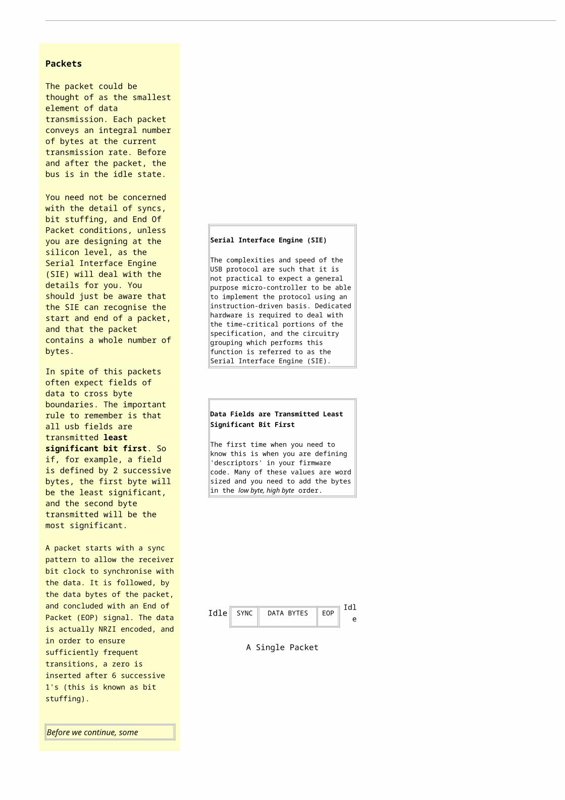
3. The Error Frame
Summary: (everyone, aloud) “OH DEAR, LET’S TRY AGAIN”
Simply put, the Error Frame is a special message that violates the framing rules of a CAN message. It is transmitted when a node detects a fault and will cause all other nodes to detect a fault – so they will send Error Frames, too. The transmitter will then automatically try to retransmit the message. There is an elaborate scheme of error counters that ensures that a node can’t destroy the bus traffic by repeatedly transmitting Error Frames.
The Error Frame consists of an Error Flag, which is 6 bits of the same value (thus violating the bit-stuffing rule) and an Error Delimiter, which is 8 recessive bits. The Error Delimiter provides some space in which the other nodes on the bus can send their Error Flags when they detect the first Error Flag.
Here’s the Error Frame:
4. The Overload Frame
Summary: “I’m a very busy little 82526, could you please wait for a moment?”
The Overload Frame is mentioned here just for completeness. It is very similar to the Error Frame with regard to the format and it is transmitted by a node that becomes too busy. The Overload Frame is not used very often, as today’s CAN controllers are clever enough not to use it. In fact, the only controller that will generate Overload Frames is the now obsolete 82526.
Standard vs. Extended CAN
Originally, the CAN standard defined the length of the Identifier in the Arbitration Field to eleven (11) bits. Later on, customer demand forced an extension of the standard. The new format is often called Extended CAN and allows no less than twenty-nine (29) bits in the Identifier. To differentiate between the two frame types, a reserved bit in the Control Field was used.
The standards are formally called
2.0A, with 11-bit Identifiers only, 2.0B, extended version with the full 29-bit Identifiers (or the 11-bit, you can mix them.) A 2.0B node can be
o “2.0B active”, i.e. it can transmit and receive extended frames, or
o “2.0B passive”, i.e. it will silently discard received extended frames (but see below.)
1.x refers to the original specification and its revisions.
New CAN controllers today are usually of the 2.0B type. A 1.x or 2.0A type controller will get very upset if it receives messages with 29 arbitration bits. A 2.0B passive type controller will tolerate them, acknowledge them if they are correct and then – discard them; a 2.0B active type controller can both transmit and receive them.
Controllers implementing 2.0B and 2.0A (and 1.x) are compatible – and may be used on the same bus – as long as the controllers implementing 2.0B refrain from sending extended frames!
Sometimes people advocate that standard CAN is “better” than Extended CAN because there is more overhead in the Extended CAN messages. This is not necessarily true. If you use the Arbitration Field for transmitting data, then Extended CAN may actually have a lower overhead than Standard CAN has.