Embed Size (px)
Citation preview
C H A P T E R 4WDM Network Design -1
Introduction to Optical DesignA network planner needs to optimize the various electrical and optical parameters to ensure smooth operations of a wavelength division multiplexing (WDM) network. Whether the network topology is that of a point-to-point link, a ring, or a mesh, system design inherently can be considered to be of two separate parts: optical system design and electrical or higher-layer system design. To the networking world, the optical layer (WDM layer) appears as a barren physical layer whose function is to transport raw bits at a high bit rate with negligible loss. Most conventional network layer planners do not care about the heuristics of the optical layer.
However, such lapses can often be catastrophic. Until the bit rate and the transmission distance is under some bounded constraint (for example, small networks), it is often not important to consider the optical parameters.
However, as the bit rate increases and transmission length increases, these optical param-eters have the capability of playing truant in the network. A network planner must consider the affecting parameters and build a network that accommodates the impairments caused by the optical parameters. This chapter explores some of the design constraints involved in the WDM network design.
Consider an optical signal as a slowly varying signal of amplitude A (τ, t) (function of distance 'τ' and time 't'), on which various parameters are acting at all times. An optical signal, as discussed in Chapter 1, “Introduction to Optical Networking,” propagates through a silica fiber with propagation constant β, whose value is obtained from the solution of the basic wave equations. Further, this optical signal is subjected to attenuation, which by virtue of itself, is a property of the propagating medium—silica fiber in this case. Attenu-ation in a fiber is characterized by the attenuation constant α, which gives the loss (in dB) per traveled km.
Why is attenuation parameter important? First, common thinking says that if the total accumulated attenuation is greater than the signal input launch power Pin, a signal will not exist at the receiving end. This, although colloquial, is an important issue for verifying signal reception at the receiving end of a communication channel. Second, for optical communication to happen, a receiver (essentially a photodetector, either a PIN or APD
0749.book Page 109 Monday, November 11, 2002 10:28 AM
110 Chapter 4: WDM Network Design -1
type) needs a minimum amount of power to distinguish the 0s and 1s from the raw input optical signal.
The minimum power requirement of the receiver is called the receiver sensitivity, R, and is covered in Chapter 2, “Networking with DWDM-1.” Here, we must ensure that the transmit power is high enough so that it can maintain signal power > R at the receiver end, despite the attenuation along the transmission line. That does not mean that if we increase the transmit power to a high level, we can send bits across great distances. High input power also is a breeding ground for impairments (nonlinearities such as cross-phase modulation [XPM], self-phase modulation [SPM], four-wave mixing [FWM] and so on). In addition, an upper limit exists for every receiver (APD type or PIN type) for receiving optical power. This is given by the dynamic range of the receiver, and it sets the maximum and minimum power range for the receiver to function. For example, –7 dBm to –28 dBm is a typical dynamic range of a receiver. Therefore, the maximum input power that we can launch into the fiber is limited. This also limits the maximum transmission distance, L. If PinMax is the maximum input power, the transmission distance is L, and Pr is the minimum receiver power; then Equation 4-1 shows the maximum input power that can be sent into the fiber and Equation 4-2 shows the maximum transmission distance.
Equation 4-1
Equation 4-2
NOTE The optical power at the receiver end has to be within the dynamic range of the receiver; otherwise, it damages the receiver (if it exceeds the maximum value) or the receiver cannot differentiate between 1s and 0s if the power level is less than the minimum value.
For an input power of +5 dB and a receiver sensitivity of –20 dBm at 1550 nm, the maximum transmission distance without amplification is shown in the following equation. (Assume α = 0.2 dB/km at 1550 nm. We usually get α from the manufacture’s spec.)
PinmaxdB( ) αL Pr dB( )+=
LPin Pr–
α-------------------=
km. (Here we neglected all other losses.)L5 20–( )–
0.2----------------------- 125= =
0749.book Page 110 Monday, November 11, 2002 10:28 AM
Introduction to Optical Design 111
Further in the preceding calculation, we have neglected dispersion, fiber nonlinearities, polarization, spectral broadening, chirp (source broadening), fiber plant losses (connecters, splices, and aging factors), and so on. If we consider these effects, then the maximum length is reduced further. How can we then have ultra long-haul intercontinental systems? By placing repeaters in cascade, we can enhance the transmission distance.
Two kinds of repeaters exist: opto-electro-opto (OEO) electrical repeaters that detect, reshape, retime, and retransmit (3R) the signal (channel-by-channel), and the fiber ampli-fiers (1R)(doped fiber, Raman, and SOA) that boost the signal power level (no reshape and no retiming) entirely in the optical domain. A third technique also exists: reshape and reamplify (2R) regeneration. This technique is gaining in popularity due to its protocol independence. This book discussed 2R in Chapter 2, so it is not necessary to consider it here from a design perspective because it proposes a generic alternative to the other design schemes.
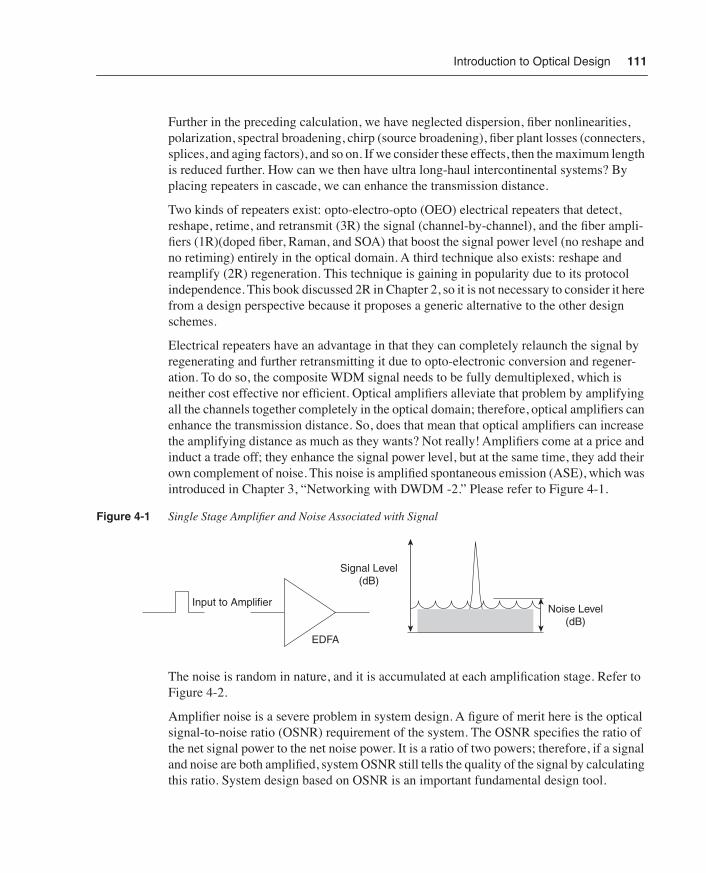
Electrical repeaters have an advantage in that they can completely relaunch the signal by regenerating and further retransmitting it due to opto-electronic conversion and regener-ation. To do so, the composite WDM signal needs to be fully demultiplexed, which is neither cost effective nor efficient. Optical amplifiers alleviate that problem by amplifying all the channels together completely in the optical domain; therefore, optical amplifiers can enhance the transmission distance. So, does that mean that optical amplifiers can increase the amplifying distance as much as they wants? Not really! Amplifiers come at a price and induct a trade off; they enhance the signal power level, but at the same time, they add their own complement of noise. This noise is amplified spontaneous emission (ASE), which was introduced in Chapter 3, “Networking with DWDM -2.” Please refer to Figure 4-1.
Figure 4-1 Single Stage Amplifier and Noise Associated with Signal
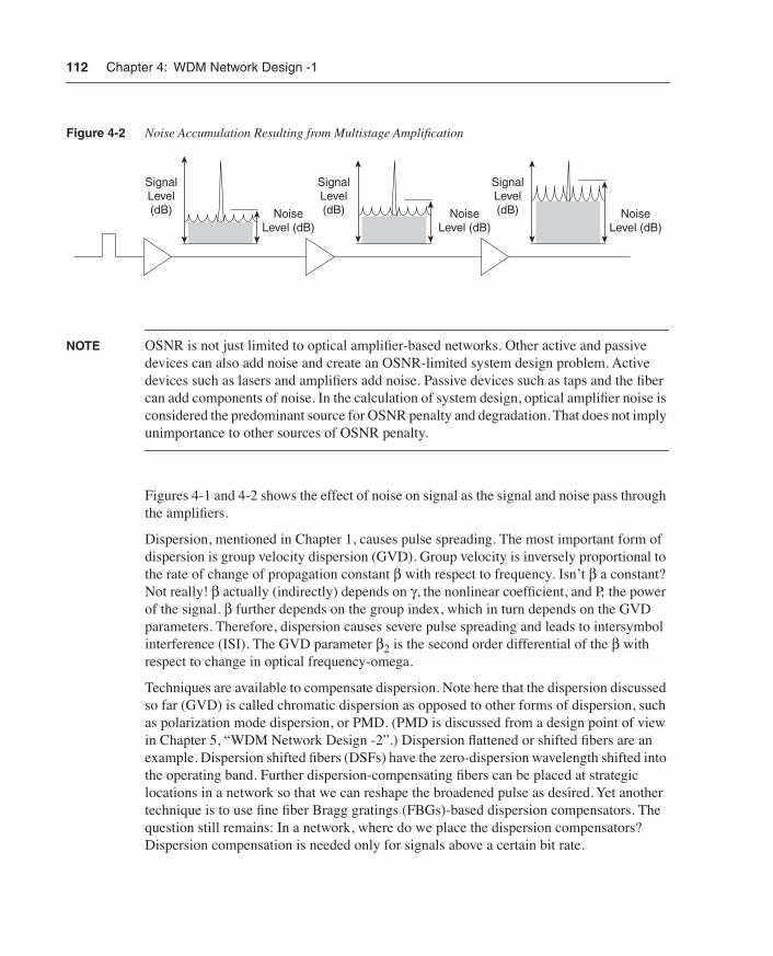
The noise is random in nature, and it is accumulated at each amplification stage. Refer to Figure 4-2.
Amplifier noise is a severe problem in system design. A figure of merit here is the optical signal-to-noise ratio (OSNR) requirement of the system. The OSNR specifies the ratio of the net signal power to the net noise power. It is a ratio of two powers; therefore, if a signal and noise are both amplified, system OSNR still tells the quality of the signal by calculating this ratio. System design based on OSNR is an important fundamental design tool.
0749.book Page 111 Monday, November 11, 2002 10:28 AM
112 Chapter 4: WDM Network Design -1
Figure 4-2 Noise Accumulation Resulting from Multistage Amplification
NOTE OSNR is not just limited to optical amplifier-based networks. Other active and passive devices can also add noise and create an OSNR-limited system design problem. Active devices such as lasers and amplifiers add noise. Passive devices such as taps and the fiber can add components of noise. In the calculation of system design, optical amplifier noise is considered the predominant source for OSNR penalty and degradation. That does not imply unimportance to other sources of OSNR penalty.
Figures 4-1 and 4-2 shows the effect of noise on signal as the signal and noise pass through the amplifiers.
Dispersion, mentioned in Chapter 1, causes pulse spreading. The most important form of dispersion is group velocity dispersion (GVD). Group velocity is inversely proportional to the rate of change of propagation constant β with respect to frequency. Isn’t β a constant? Not really! β actually (indirectly) depends on γ, the nonlinear coefficient, and P, the power of the signal. β further depends on the group index, which in turn depends on the GVD parameters. Therefore, dispersion causes severe pulse spreading and leads to intersymbol interference (ISI). The GVD parameter β2 is the second order differential of the β with respect to change in optical frequency-omega.
Techniques are available to compensate dispersion. Note here that the dispersion discussed so far (GVD) is called chromatic dispersion as opposed to other forms of dispersion, such as polarization mode dispersion, or PMD. (PMD is discussed from a design point of view in Chapter 5, “WDM Network Design -2”.) Dispersion flattened or shifted fibers are an example. Dispersion shifted fibers (DSFs) have the zero-dispersion wavelength shifted into the operating band. Further dispersion-compensating fibers can be placed at strategic locations in a network so that we can reshape the broadened pulse as desired. Yet another technique is to use fine fiber Bragg gratings (FBGs)-based dispersion compensators. The question still remains: In a network, where do we place the dispersion compensators? Dispersion compensation is needed only for signals above a certain bit rate.
0749.book Page 112 Monday, November 11, 2002 10:28 AM
Factors That Affect System Design 113
Another design issue is polarization. Assuming fibers to be polarization preserving is not a good idea. Different polarization states create different levels of PMD. PMD compensation and placement is yet another strong issue at high bit rate signals.
Last but not least, we need to consider fiber nonlinearities. Self-phase modulation and cross phase modulation are two common coupling problems. FWM, stimulated Raman scattering (SRS), and stimulated Brillouin scattering (SBS) are also high bit rate, high power issues.
A system design can be optimized by considering these effects in a strategic manner. The sections that follow consider several steps that need to be considered in an ideal system design case. Initially, let’s assume a point-to-point link and then specifically look at ring and mesh networks in Chapter 5.
Factors That Affect System DesignInitially, fiber loss was considered the biggest factor in limiting the length of an optical channel. However, as data rates grew and pulses occupied lesser and lesser time slots, group velocity dispersion and nonlinearities (SPM, XPM, and FWM) became important consid-erations.
As we will see in the following sections, an optical link is designed by taking into account a figure of merit, which is generally the bit error rate (BER) of the system. For most practical WDM networks, this requirement of BER is 10-12 (~ 10-9 to 10-12), which means that a maximum one out of every 1012 bits can be corrupted during transmission. Therefore, BER is considered an important figure of merit for WDM networks; all designs are based to adhere to that quality.
In Chapter 2, we saw the analytical explanation behind BER. It showed BER to be a ratio of the difference of high and low bit levels (power) to the difference in standard deviation of high and low bit levels. As can be observed it is quite difficult to calculate BER instan-taneously.
Another plausible explanation of BER can be considered as follows. For a photodetector to detect a 1 bit correctly (assuming nonreturn-to-zero/return-to-zero, or NRZ/RZ modulation; see Chapter 2), it needs a certain minimum number of photons (Np) falling on it. If NTP is the number of photons launched at the transmitter and ∆p is the number of photons lost (hypothetically) due to attenuation, absorption, scattering, and other impairments during transmission, then if NTP - ∆p < Np, the receiver will not be able to decode the signals properly. To sustain good communication, it is imperative that NTP – ∆p > Np over 'L' the desired length of transmission channel. The number of photons translates to the power (which is a function of intensity) of the optical signal.
From the explanation, it becomes evident why optical system design considers power budget and power margins (safety margins for good design) so important.
0749.book Page 113 Monday, November 11, 2002 10:28 AM
114 Chapter 4: WDM Network Design -1
As far as the dispersion issue goes, we know that dispersion is the spreading of a pulse in time domain, generally due to the large variance of the spectral domain. (Many different spectral components exist in a pulse, each travelling at a different speed.) That means dispersion causes pulse spreading.
The most harmful effect of this pulse spreading is ISI. Even if you assume ISI never to happen (due to good design), still a small amount of dispersion has several harmful effects. The spreading of a pulse lowers its power content, which means that ∆p increases. In other words, the number of photons that will strike the photodetector decreases. Therefore, when we are considering dispersion-limited systems, we must consider a power penalty due to dispersion. This power penalty3 can qualitatively be defined as the net loss in power because of dispersion during transmission of a signal in a dispersion affected/limited system.
Qualitatively, power penalty can also be considered as the net extra power required to pump up the signal so that it reaches the receiver (photodetector) while maintaining the minimum BER requirement of the system. Typically, the power penalty for most networks is in the range of 2–3 dB. ITU specification G957 states that this penalty should not be greater than 2 dB.
Long-Haul Impairments: NonlinearityBy placing optical amplifiers, we can greatly enhance the power of an optical signal as it reaches the photodetector. Yet another system design consideration is the net fiber nonlin-earity that is present in silica fibers. The intensity of the electromagnetic wave propagating through a fiber gives rise to nonlinearities. The refractive index has a strong nonlinear component that depends on the power level of the signal. Nonlinearity produces a nonlinear phase shift denoted by φNL. This is shown in Equation 4-3.
Equation 4-3
In Equation 4-3, is the nonlinear coefficient that is denoted by Equation 4-4.
Equation 4-4
In Equation 4-4, n2 is the cladding index, and Aeff is the area of cross-section of the core. Further φNL being dependent of Pin such that Pin by itself is a time varying response.
φNL γ Pin1 e
α– L–[ ]
α-------------------------=
γ
γn2ω0
cAeff-------------=
0749.book Page 114 Monday, November 11, 2002 10:28 AM
Factors That Affect System Design 115
Therefore, the nonlinear phase shift induced in a fast-moving optical pulse is quite dynamic.
The implication is that a frequency chirp is associated with this phase shift. In other words, a pulse at frequency ω0 would, in time, have components in the frequency range shown in the next equation.
In the equation, φNL is dynamic. The result is pulse spreading, which is a result of the power dependence on the induced phase shift. Therefore, to keep a check on the maximum phase shift that a pulse can have, it is imperative to set a threshold to the maximum input power. This nonlinear phase shift is Self Phase Modulation (SPM). In optical communication, lightpaths need to be designed, keeping in mind the maximum tolerable phase shift φNL < 1. Therefore, the maximum power [Pin max | φNL < 1] can limit phase shift to less than the system requirement.
SPM does not act alone. In optical communication, GVD and SPM often go hand in hand, acting quasi-simultaneously over a length of the fiber. The input channel power needs to be optimized so that it ensures a net dispersion (at a given bit rate) that is less than the minimum tolerable dispersion, as well as for which the net nonlinear effects are under control. In other words, a tradeoff is involved: We need some more power to take care of the dispersion-induced power penalty, but this additional power leads to fiber nonlinear effects (such as SPM), which creates more spread.
An optimization technique involves simulation, whereby we can correctly design the network by considering all the affecting factors and using the appropriate entities to com-pensate for these factors. In one method, SPM and GVD are both calculated on a split Fourier transform. Using this method, frequency domain analysis of the two effects is accomplished by breaking the cylindrical waveguide (fiber) into infinitesimal overlapping segments, such that SPM is assumed to act on odd segments and GVD is set to act on even segments. The final sum of effects on the last and penultimate segments gives the net impairment in the system.
So far, nonlinearities have been considered on just one channel. What happens when we have a WDM system? Do parallel channels have an effect on each other? Two or more channels have nonlinear effects on each other: XPM and FWM. Cross phase modulation results from the different carrier frequency of independent channels, including the associated phase shifts on one another. Cross phase modulation is severely harmful and is twice as powerful as Self phase modulation. The induced phase shift is due to the “walkover” effect, whereby two pulses at different bit rates or with different group velocities walk across each other. The slower pulse sees the walkover and induces a phase shift because of this walkover effect. The total phase shift depends on the net power of all the channels and on the bit output of the
ω0 φNL±
0749.book Page 115 Monday, November 11, 2002 10:28 AM
116 Chapter 4: WDM Network Design -1
channels. Maximum phase shift is produced when two 1 bits walk across each other due to the high power in both the bits (as opposed to the lower power levels when both bits are not at logical 1).
Mathematically, the phase shift is shown in Equation 4-5.
Equation 4-5
In Equation 4-5, w is the total number of channels and Pk is the power of the kth channel. The maximum phase shift (for all 1 bits) is shown in Equation 4-6.
Equation 4-6
NOTE Another method is to solve Schrödinger’s nonlinear propagation equation shown in the next equation.
Effect of Chromatic Dispersion on Transmission Length and Induced Power Penalty
Group velocity dispersion (chromatic dispersion) is a primary cause of concern in high bit rate (> 2.5 Gbps) single-mode WDM systems. As explained previously, dispersion in an optical pulse creates pulse broadening such that the pulse spreads into the slots (in the time domain) of the other pulses. This not only causes ISI, but it also introduces a power penalty, which can cause degradation of the system’s SNR. As shown in the next section, OSNR is a true figure of merit for optical communications. The power penalty due to dispersion is shown in Equation 4-7.
φiNL γ 1 e
αL––
α-------------------- Pi 2Σ P
wk
K 1=K 1≠
+=
φmaxNL γ
α--- 2w 1–[ ]Pi=
∂A∂z------
i2---β2
∂2A
∂t2
---------16---β3
∂3A
∂t3
--------- iγ A A2 α
2--- A–=–+
0749.book Page 116 Monday, November 11, 2002 10:28 AM
Design of a Point-to-Point Link Based on Q-Factor and OSNR 117
Equation 4-7
In the preceding equation, is the spectral width and is the pulse width. Further for SMF fibers, dispersion parameter D = 17 ps/Km – nm. The limit on transmission distance is shown as in Equation 4-8.
Equation 4-8
Therefore, the following equation is true.
K is a constant; therefore, as B increases, L decreases with the square root of B.
Design of a Point-to-Point Link Based on Q-Factor and OSNR
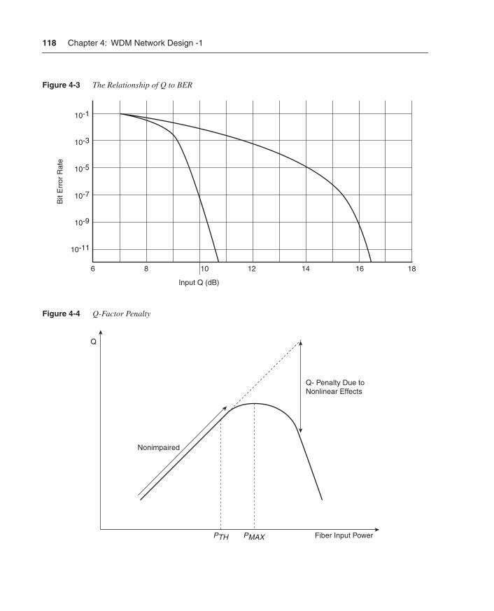
To design a network, it is imperative to comply the system design with the BER require-ment of the network. If one carefully considers the preceding criteria, it should be evident that calculating BER instantaneously is an intriguing task given that a designer has tools such as a spreadsheet and calculator. Chapter 2 briefly discussed the Q-factor of an optical signal. The Q-factor provides a qualitative description of the receiver performance because it is a function of the signal to noise ratio (optical). The Q-factor suggests the minimum SNR required to obtain a specific BER for a given signal. Figure 4-3 shows the relationship of Q-factor to BER. As we can see, the higher the value of Q-factor, the better the BER.
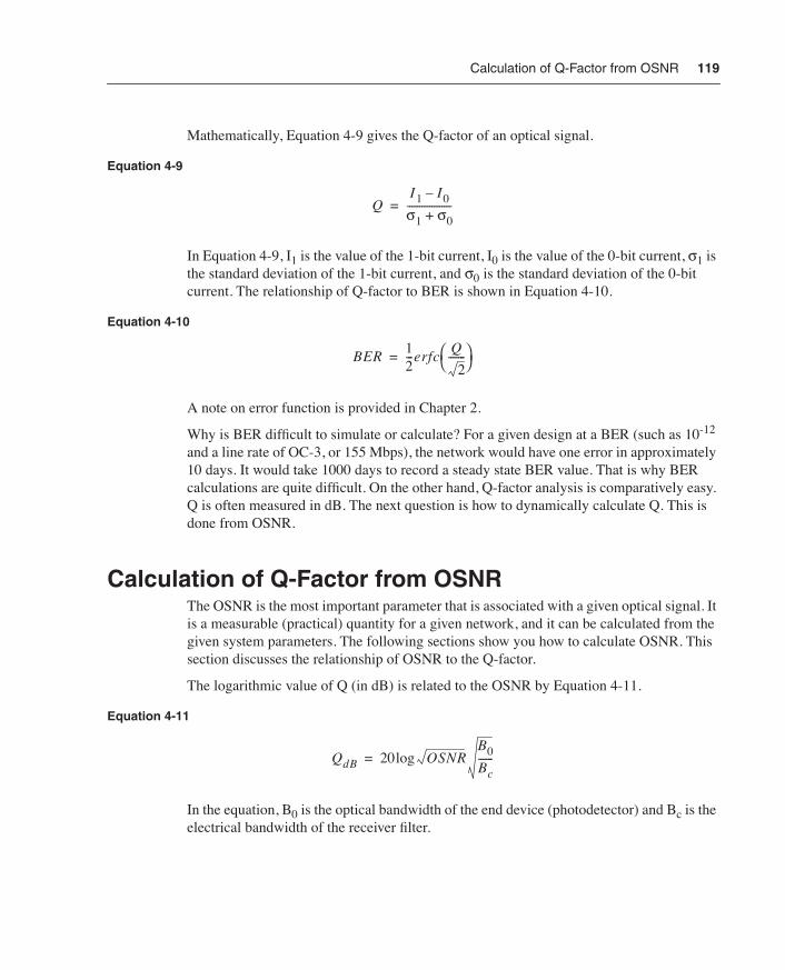
Figure 4-4 shows the penalty of the Q-factor due to nonlinear effects by increase in input power.
PenaltyDISP
10 σσ0------log
1 DL
σλσ0------
2
+
------------------------------------=
σλ σ0
or B2L 16
λ2D
2πc----------< L
16
B2
------λ2D
2πc----------<
LK
B2
------<
0749.book Page 117 Monday, November 11, 2002 10:28 AM
118 Chapter 4: WDM Network Design -1
Figure 4-3 The Relationship of Q to BER
Figure 4-4 Q-Factor Penalty
0749.book Page 118 Monday, November 11, 2002 10:28 AM
Calculation of Q-Factor from OSNR 119
Mathematically, Equation 4-9 gives the Q-factor of an optical signal.
Equation 4-9
In Equation 4-9, I1 is the value of the 1-bit current, I0 is the value of the 0-bit current, σ1 is the standard deviation of the 1-bit current, and σ0 is the standard deviation of the 0-bit current. The relationship of Q-factor to BER is shown in Equation 4-10.
Equation 4-10
A note on error function is provided in Chapter 2.
Why is BER difficult to simulate or calculate? For a given design at a BER (such as 10-12 and a line rate of OC-3, or 155 Mbps), the network would have one error in approximately 10 days. It would take 1000 days to record a steady state BER value. That is why BER calculations are quite difficult. On the other hand, Q-factor analysis is comparatively easy. Q is often measured in dB. The next question is how to dynamically calculate Q. This is done from OSNR.
Calculation of Q-Factor from OSNRThe OSNR is the most important parameter that is associated with a given optical signal. It is a measurable (practical) quantity for a given network, and it can be calculated from the given system parameters. The following sections show you how to calculate OSNR. This section discusses the relationship of OSNR to the Q-factor.
The logarithmic value of Q (in dB) is related to the OSNR by Equation 4-11.
Equation 4-11
In the equation, B0 is the optical bandwidth of the end device (photodetector) and Bc is the electrical bandwidth of the receiver filter.
QI1 I0–
σ1 σ0+------------------=
BER12---erfc
Q
2-------
=
QdB 20 OSNRB0
Bc------log=
0749.book Page 119 Monday, November 11, 2002 10:28 AM
120 Chapter 4: WDM Network Design -1
Therefore, Q(dB) is shown in Equation 4-12.
Equation 4-12
In other words, Q is somewhat proportional to the OSNR. Generally, noise calculations are performed by optical spectrum analyzers (OSAs) or sampling oscilloscopes, and these measurements are carried over a particular measuring range of Bm. Typically, Bm is approx-imately 0.1 nm or 12.5 GHz for a given OSA. From Equation 4-12, showing Q in dB in terms of OSNR, it can be understood that if B0 < Bc, then OSNR (dB )> Q (dB). For practical designs OSNR(dB) > Q(dB), by at least 1–2 dB. Typically, while designing a high-bit rate system, the margin at the receiver is approximately 2 dB, such that Q is about 2 dB smaller than OSNR (dB).
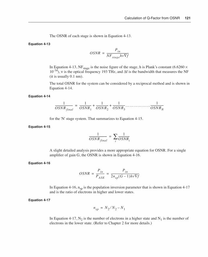
Calculation of OSNR for a Point-to-Point LinkConsider a physical link AB, as shown in Figure 4-5. Assume this to be a long-haul fiber WDM link (a link that is several hundred kilometers). Amplifiers are placed periodically at repeated intervals to boost signal power. Therefore, a signal can reach much farther than the maximum allowable accumulated loss due to the fiber (∝L). However, in doing so, each amplifier stage adds its own component of amplified spontaneous emission (ASE) noise and degrades the OSNR further. Moreover, every amplifier amplifies the already present noise. Note that noise is omnipresent throughout the spectra and almost impossible to be removed. Therefore, it is imperative to devise a method to calculate the OSNR (output) at the end of an N stage-amplified system and see if the value N is still valid.
In an OSNR-based design, we must ensure that OSNR of the final stage is in compliance with system OSNR requirements and hence the BER requirements. To make the system support a particular BER, it is necessary to make the OSNR system design compliant.
Figure 4-5 A Multiple Stage Amplified DWDM System Deployed in a Point-to-Point Topology
QdB OSNR 10B0
Bc------log+=
0749.book Page 120 Monday, November 11, 2002 10:28 AM
Calculation of Q-Factor from OSNR 121
The OSNR of each stage is shown in Equation 4-13.
Equation 4-13
In Equation 4-13, NFstage is the noise figure of the stage, h is Plank’s constant (6.6260 × 10⁻³⁴), ν is the optical frequency 193 THz, and ∆f is the bandwidth that measures the NF (it is usually 0.1 nm).
The total OSNR for the system can be considered by a reciprocal method and is shown in Equation 4-14.
Equation 4-14
for the 'N' stage system. That summarizes to Equation 4-15.
Equation 4-15
A slight detailed analysis provides a more appropriate equation for OSNR. For a single amplifier of gain G, the OSNR is shown in Equation 4-16.
Equation 4-16
In Equation 4-16, nsp is the population inversion parameter that is shown in Equation 4-17 and is the ratio of electrons in higher and lower states.
Equation 4-17
In Equation 4-17, N2 is the number of electrons in a higher state and N1 is the number of electrons in the lower state. (Refer to Chapter 2 for more details.)
OSNRPin
NFstagehv∇f----------------------------------=
1OSN R final--------------------------- 1
OSNR1------------------ 1
OSN R2-------------------
1OSN R3-------------------……………… 1
OSN RN--------------------+ +=
1OSN R final--------------------------- 1
OSNRi-----------------
i∑=
OSNRPin
PASE-------------
Pin
2nsp G 1–( )hv∇f-------------------------------------------= =
nsp N2 N2 N1–⁄=
0749.book Page 121 Monday, November 11, 2002 10:28 AM
122 Chapter 4: WDM Network Design -1
The population inversion parameter is also shown in Equation 4-18.
Equation 4-18
For an N amplifier stage system, with each amplifier compensating for the loss of the previous span where the span loss in dB is , you have the relationship for final stage OSNR in Equation 4-19.
Equation 4-19
Taking logarithm to the common base (10), we get Equation 4-20.
Equation 4-20
From the previous section, we get ∇f = 0.1 nm, or 12.5 GHz. Substituting this, we get Equation 4-21.
Equation 4-21
The following is assumed:
• The NF of every amplifier is the same. (we assume uniformity of products; therefore, NFs are the same for all amplifiers.)
• is the span loss and is same. (This is a generic assumption and can be changed, as shown later in this section.)
• Noise is totaled over both states of polarization. In short, it is unpolarized noise.
Equation 4-21 provides the actual mathematical calculation of OSNR. This calculation method has quite a few approximations in which we can still find the system OSNR to a great degree of accuracy. In a multichannel WDM system, the design should consider OSNR for the worst channel (the one that has the worst impairment). The worst channel is generally the first or last channel in the spectrum.
nsp 0.5 10
NF10--------
×=
OSNR final
Pin
NFΓhr∇ f .N---------------------------------=
OSN Rdb 158.93 Pin db( ) NFdb– 10 N 10 ∇flog–log––+=
OSN Rdb 58 Pin db( ) NFdb– 10 Nlog––+=
0749.book Page 122 Monday, November 11, 2002 10:28 AM
Calculation of Q-Factor from OSNR 123
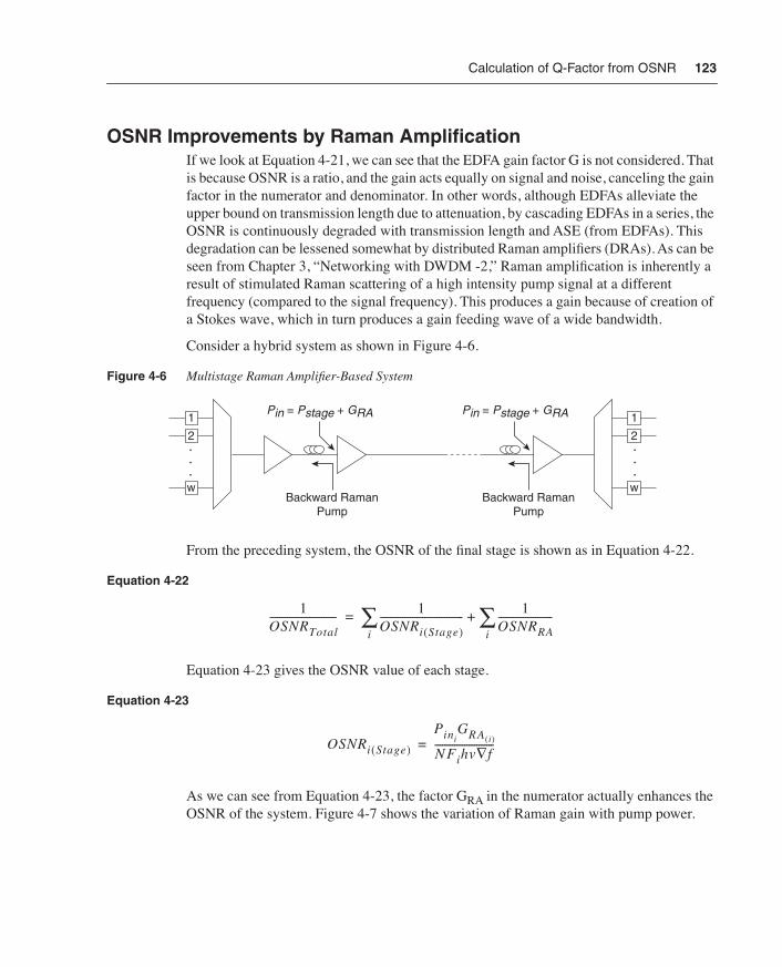
OSNR Improvements by Raman AmplificationIf we look at Equation 4-21, we can see that the EDFA gain factor G is not considered. That is because OSNR is a ratio, and the gain acts equally on signal and noise, canceling the gain factor in the numerator and denominator. In other words, although EDFAs alleviate the upper bound on transmission length due to attenuation, by cascading EDFAs in a series, the OSNR is continuously degraded with transmission length and ASE (from EDFAs). This degradation can be lessened somewhat by distributed Raman amplifiers (DRAs). As can be seen from Chapter 3, “Networking with DWDM -2,” Raman amplification is inherently a result of stimulated Raman scattering of a high intensity pump signal at a different frequency (compared to the signal frequency). This produces a gain because of creation of a Stokes wave, which in turn produces a gain feeding wave of a wide bandwidth.
Consider a hybrid system as shown in Figure 4-6.
Figure 4-6 Multistage Raman Amplifier-Based System
From the preceding system, the OSNR of the final stage is shown as in Equation 4-22.
Equation 4-22
Equation 4-23 gives the OSNR value of each stage.
Equation 4-23
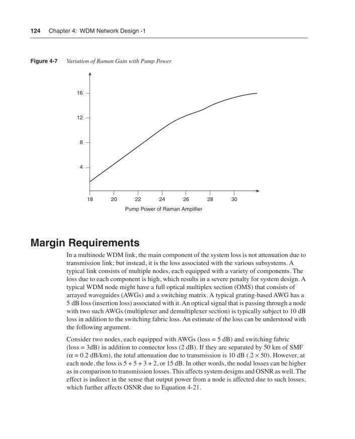
As we can see from Equation 4-23, the factor GRA in the numerator actually enhances the OSNR of the system. Figure 4-7 shows the variation of Raman gain with pump power.
1OSNRTotal--------------------------- 1
OSNRi Stage( )---------------------------------- 1
OSNRRA----------------------
i∑+
i∑=
OSNRi Stage( )
PiniGR A i( )
NFihv∇f------------------------=
0749.book Page 123 Monday, November 11, 2002 10:28 AM
124 Chapter 4: WDM Network Design -1
Figure 4-7 Variation of Raman Gain with Pump Power
Margin RequirementsIn a multinode WDM link, the main component of the system loss is not attenuation due to transmission link; but instead, it is the loss associated with the various subsystems. A typical link consists of multiple nodes, each equipped with a variety of components. The loss due to each component is high, which results in a severe penalty for system design. A typical WDM node might have a full optical multiplex section (OMS) that consists of arrayed waveguides (AWGs) and a switching matrix. A typical grating-based AWG has a 5 dB loss (insertion loss) associated with it. An optical signal that is passing through a node with two such AWGs (multiplexer and demultiplexer section) is typically subject to 10 dB loss in addition to the switching fabric loss. An estimate of the loss can be understood with the following argument.
Consider two nodes, each equipped with AWGs (loss = 5 dB) and switching fabric (loss = 3dB) in addition to connector loss (2 dB). If they are separated by 50 km of SMF (α = 0.2 dB/km), the total attenuation due to transmission is 10 dB (.2 × 50). However, at each node, the loss is 5 + 5 + 3 + 2, or 15 dB. In other words, the nodal losses can be higher as in comparison to transmission losses. This affects system designs and OSNR as well. The effect is indirect in the sense that output power from a node is affected due to such losses, which further affects OSNR due to Equation 4-21.
0749.book Page 124 Monday, November 11, 2002 10:28 AM
Margin Requirements 125
Table 4-1 shows the insertion loss due to typical elements. We have to quantize losses due to impairments in transmission. As mentioned in the introductory section to this chapter, dispersion can be quantified as a penalty in dB. Similar treatment can be done to other phenomena such as polarization and nonlinearities and so on.
Table 4-2 presents margin requirements for a good design. These margins adhere to varia-tions in optical signal budgeting issues, especially on a dynamic level. The margins are generally chosen by evaluating a set of readings that represent the pseudo-population of a number of discrete events governing the entire sample space of optical signal design.
Table 4-1 Insertion Loss and Other Losses for 1550 nm Operation
ComponentInsertion Loss
Wavelength-Dependent Loss
Polarization-Dependent Loss
Cross-Talk NF
Multiplexer
Demultiplex (AWG)
5 dB < 1 dB 0.1 dB –40 dB
Optical 2 × 2 add-drop switch
1.2 dB < 0.2 dB 0.1 dB –40 dBm
Coupler (2 × 2) passive 3 dB - - -
Filter-Thin-film 1 dB 0.1 dB - –40 dBm
Filter- AOTF/MZI 1 dB 0.1 dB - –35 dBm
Interleaver 2–3 dB - - -
Optical cross-connect (OXC)
Port to port
3 dB typical without AWG loss
< 0.4 dB 0.1 dB –40 dBm
Table 4-2 Margin Requirements
Symptom Loss Margin
Fiber dispersion 1 dB
SPM margin 0.5 dB
XPM margin 0.5 dB
DCU compensation 6 dB
FWM 0.5 dB
SRS/SBS 0.5 dB
PDL 0.3 dB
continues
0749.book Page 125 Monday, November 11, 2002 10:28 AM
126 Chapter 4: WDM Network Design -1
Design Using Chromatic Dispersion CompensationIn a chromatic dispersion-limited system in which the total accumulated dispersion for a traveling pulse is greater than the maximum allowable dispersion, the system cannot function because of tremendous ISI or just pure pulse spread. Therefore, we need to place dispersion compensation units (DCUs) at different positions in a network. Chapter 3 discussed some of the dispersion-compensating schemes, such as dispersion shifted fibers and FBGs, which are the most common. When we are designing a high bit rate WDM link (where dispersion can be considered a major design impairment), we should use dispersion maps to effectively design a system.
Dispersion maps are two-dimensional maps that plot the accumulated dispersion versus the length of transmission. They are particularly useful maps that help designers tell where to place dispersion compensators in a network. Accumulated dispersion is calculated by multiplying the fiber and the laser dispersion specifications for a given bit rate with respect to the length of the fiber. For example, an SMF fiber’s typical value of dispersion is 16 ps/nm-km, which means that for every traversed kilometer of SMF fiber, a pulse at 10 Gbps (100 ps pulse width) spreads for about 16 ps from its mean. Ensure that the accumulated pulse spread across 'x' km is less than the maximum dispersion limit (which might be 1600 ps/km-nm for a 10 Gbps signal).
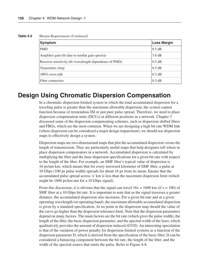
From this discussion, it is obvious that the signal can travel 16x = 1600 km (if x = 100) of SMF fiber at a 10 Gbps bit rate. It is important to note that as the signal traverses a greater distance, the accumulated dispersion also increases. For a given bit rate and at a given operating wavelength (or operating band), the maximum allowable accumulated dispersion is given by a standard specification. At no point in the dispersion map should the value of the curve go higher than the dispersion tolerance limit. Note that the dispersion parameters depend on many factors. The main factors are the bit rate (which gives the pulse width), the length of the fiber, the basic dispersion parameter, and the spectral width of the laser, which qualitatively provides the amount of dispersion induced (GVD). An interesting speculation is that of the variation of power penalty for dispersion-limited systems as a function of the dispersion parameter D, which is derived from the specification of the basic fiber. D can be considered a balancing component between the bit rate, the length of the fiber, and the width of the spectral source that emits the pulse. Refer to Figure 4-8.
PMD 0.5 dB
Amplifier gain tilt (due to nonflat gain spectra) 3.0 dB
Receiver sensitivity tilt (wavelength dependence of PMD) 0.5 dB
Transmitter chirp 0.5 dB
AWG cross-talk 0.2 dB
Fiber connectors 0.5 dB
Table 4-2 Margin Requirements (Continued)
Symptom Loss Margin
0749.book Page 126 Monday, November 11, 2002 10:28 AM
Design Using Chromatic Dispersion Compensation 127
Figure 4-8 Variation of Dispersion Parameter D with Power Penalty
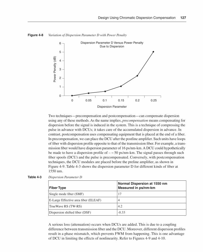
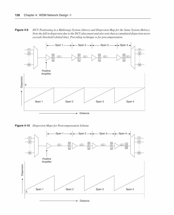
Two techniques—precompensation and postcompensation—can compensate dispersion using any of these methods. As the name implies, precompensation means compensating for dispersion before the signal is induced in the system. This is a technique of compressing the pulse in advance with DCUs; it takes care of the accumulated dispersion in advance. In contrast, postcompensation uses compensating equipment that is placed at the end of a fiber. In precompensation, we can place the DCU after the postline amplifier. Such units have loops of fiber with dispersion profile opposite to that of the transmission fiber. For example, a trans-mission fiber would have dispersion parameter of 16 ps/nm-km. A DCU could hypothetically be made to have a dispersion profile of – ~ 50 ps/nm-km. The signal passes through such fiber spools (DCU) and the pulse is precompensated. Conversely, with postcompensation techniques, the DCU modules are placed before the preline amplifier, as shown in Figure 4-9. Table 4-3 shows the dispersion parameter D for different kinds of fiber at 1550 nm.
A serious loss (attenuation) occurs when DCUs are added. This is due to a coupling difference between transmission fiber and the DCU. Moreover, different dispersion profiles result in a phase mismatch, which prevents FWM from happening. This is one advantage of DCU in limiting the effects of nonlinearity. Refer to Figures 4-9 and 4-10.
Table 4-3 Dispersion Parameter D
Fiber TypeNormal Dispersion at 1550 nm Measured in ps/nm-km
Single mode fiber (SMF) 17
E-Large Effective area fiber (ELEAF) 4
TrueWave RS (TW-RS) 4.2
Dispersion shifted fiber (DSF) -0.33
0749.book Page 127 Monday, November 11, 2002 10:28 AM
128 Chapter 4: WDM Network Design -1
Figure 4-9 DCU Positioning in a Multistage System (Above) and Dispersion Map for the Same System (Below). Note the fall in dispersion due to the DCU placement and also note that accumulated dispersion never exceeds threshold (dotted line). Preceding technique is for precompensation.
Figure 4-10 Dispersion Maps for Postcompensation Scheme
0749.book Page 128 Monday, November 11, 2002 10:28 AM
Frequency Chirp 129
OSNR and Dispersion-Based DesignFor a given network, it is important to calculate the OSNR and make a design based on both OSNR and dispersion limitations. It is possible to compensate for dispersion to a great extent. However, OSNR compensation needs 3R (O-E-O) regeneration, which is expensive. In other words, OSNR compensation is almost impossible for multichannel WDM systems. Therefore, when we are designing a WDM link, it is imperative to first consider OSNR’s limitations. OSNR-based design essentially means whether the OSNR at the final stage (at the receiver) is in conformity with the OSNR that is desired to achieve the required BER. This also guarantees the BER requirement that is essential for generating revenue.
Following OSNR-based design, dispersion is the next issue to compensate from a design perspective. Dispersion-compensating units are readily available, but an important issue is where to place them. Various algorithms have been suggested depending on the network topology, the transmission length, and the bit rates. For most designs, optimization place-ments have to be done on a span (per length) basis.
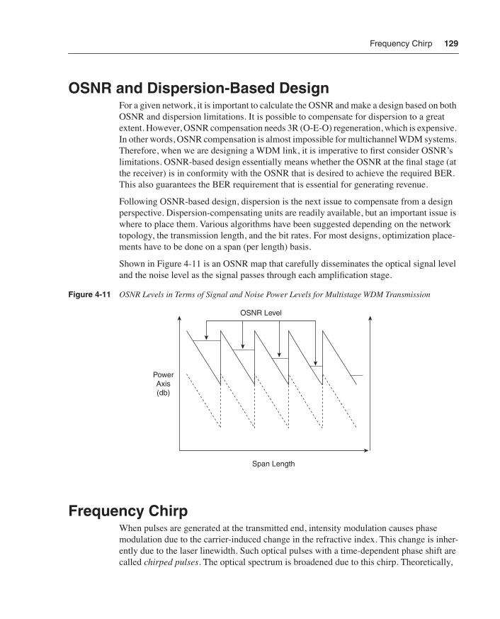
Shown in Figure 4-11 is an OSNR map that carefully disseminates the optical signal level and the noise level as the signal passes through each amplification stage.
Figure 4-11 OSNR Levels in Terms of Signal and Noise Power Levels for Multistage WDM Transmission
Frequency ChirpWhen pulses are generated at the transmitted end, intensity modulation causes phase modulation due to the carrier-induced change in the refractive index. This change is inher-ently due to the laser linewidth. Such optical pulses with a time-dependent phase shift are called chirped pulses. The optical spectrum is broadened due to this chirp. Theoretically,
0749.book Page 129 Monday, November 11, 2002 10:28 AM
130 Chapter 4: WDM Network Design -1
the chirp-induced power penalty is difficult to calculate, but it can be approximated to a 0.5 dB margin in system design (Chirp is also defined in Chapter 2.)
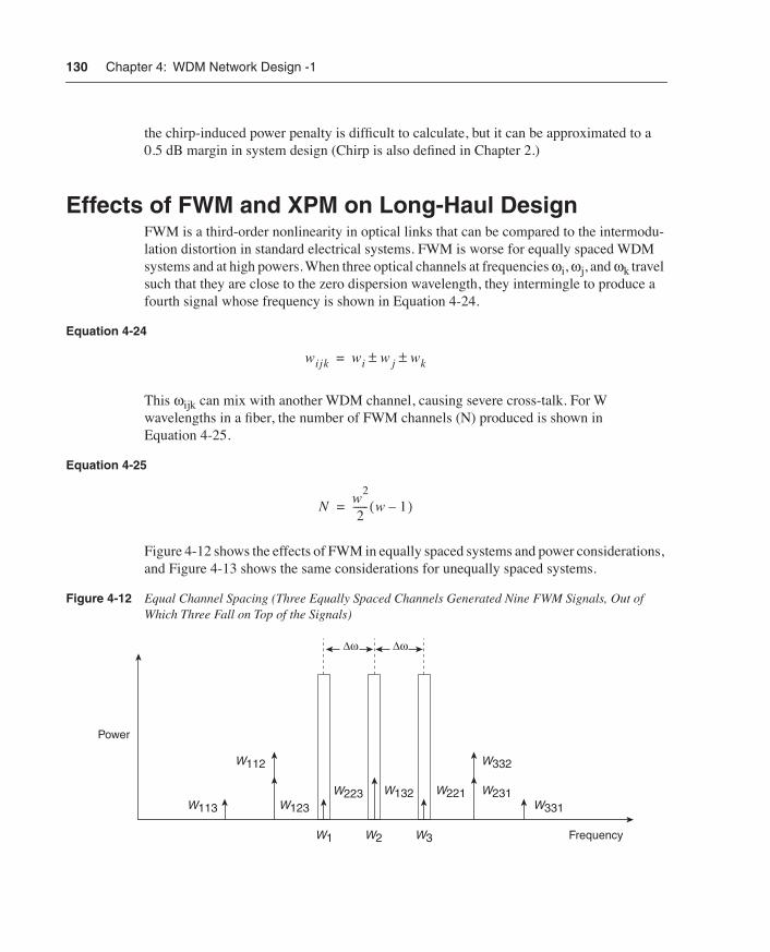
Effects of FWM and XPM on Long-Haul DesignFWM is a third-order nonlinearity in optical links that can be compared to the intermodu-lation distortion in standard electrical systems. FWM is worse for equally spaced WDM systems and at high powers. When three optical channels at frequencies ωi, ωj, and ωk travel such that they are close to the zero dispersion wavelength, they intermingle to produce a fourth signal whose frequency is shown in Equation 4-24.
Equation 4-24
This ωijk can mix with another WDM channel, causing severe cross-talk. For W wavelengths in a fiber, the number of FWM channels (N) produced is shown in Equation 4-25.
Equation 4-25
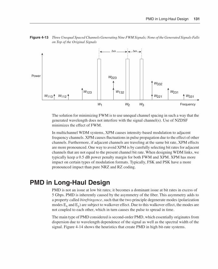
Figure 4-12 shows the effects of FWM in equally spaced systems and power considerations, and Figure 4-13 shows the same considerations for unequally spaced systems.
Figure 4-12 Equal Channel Spacing (Three Equally Spaced Channels Generated Nine FWM Signals, Out of Which Three Fall on Top of the Signals)
wijk wi w j wk±±=
Nw
2
2------ w 1–( )=
0749.book Page 130 Monday, November 11, 2002 10:28 AM
PMD in Long-Haul Design 131
Figure 4-13 Three Unequal Spaced Channels Generating Nine FWM Signals; None of the Generated Signals Falls on Top of the Original Signals
The solution for minimizing FWM is to use unequal channel spacing in such a way that the generated wavelength does not interfere with the signal channel(s). Use of NZDSF minimizes the effect of FWM.
In multichannel WDM systems, XPM causes intensity-based modulation to adjacent frequency channels. XPM causes fluctuations in pulse propagation due to the effect of other channels. Furthermore, if adjacent channels are traveling at the same bit rate, XPM effects are more pronounced. One way to avoid XPM is by carefully selecting bit rates for adjacent channels that are not equal to the present channel bit rate. When designing WDM links, we typically keep a 0.5 dB power penalty margin for both FWM and XPM. XPM has more impact on certain types of modulation formats. Typically, FSK and PSK have a more pronounced impact than pure NRZ and RZ coding.
PMD in Long-Haul DesignPMD is not an issue at low bit rates; it becomes a dominant issue at bit rates in excess of 5 Gbps. PMD is inherently caused by the asymmetry of the fiber. This asymmetry adds to a property called birefringence, such that the two principle degenerate modes (polarization modes Ex and Ey) are subject to walkover effect. Due to this walkover effect, the modes are not coupled to each other, which in turn causes the pulse to spread in time.
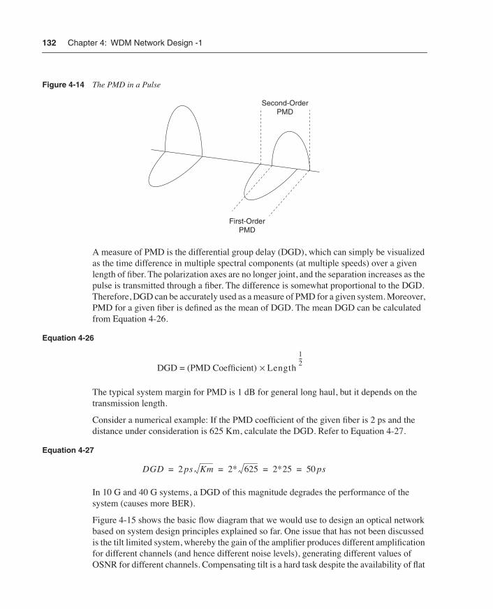
The main type of PMD considered is second-order PMD, which essentially originates from dispersion due to wavelength dependence of the signal as well as the spectral width of the signal. Figure 4-14 shows the heuristics that create PMD in high bit-rate systems.
0749.book Page 131 Monday, November 11, 2002 10:28 AM
132 Chapter 4: WDM Network Design -1
Figure 4-14 The PMD in a Pulse
A measure of PMD is the differential group delay (DGD), which can simply be visualized as the time difference in multiple spectral components (at multiple speeds) over a given length of fiber. The polarization axes are no longer joint, and the separation increases as the pulse is transmitted through a fiber. The difference is somewhat proportional to the DGD. Therefore, DGD can be accurately used as a measure of PMD for a given system. Moreover, PMD for a given fiber is defined as the mean of DGD. The mean DGD can be calculated from Equation 4-26.
Equation 4-26
The typical system margin for PMD is 1 dB for general long haul, but it depends on the transmission length.
Consider a numerical example: If the PMD coefficient of the given fiber is 2 ps and the distance under consideration is 625 Km, calculate the DGD. Refer to Equation 4-27.
Equation 4-27
In 10 G and 40 G systems, a DGD of this magnitude degrades the performance of the system (causes more BER).
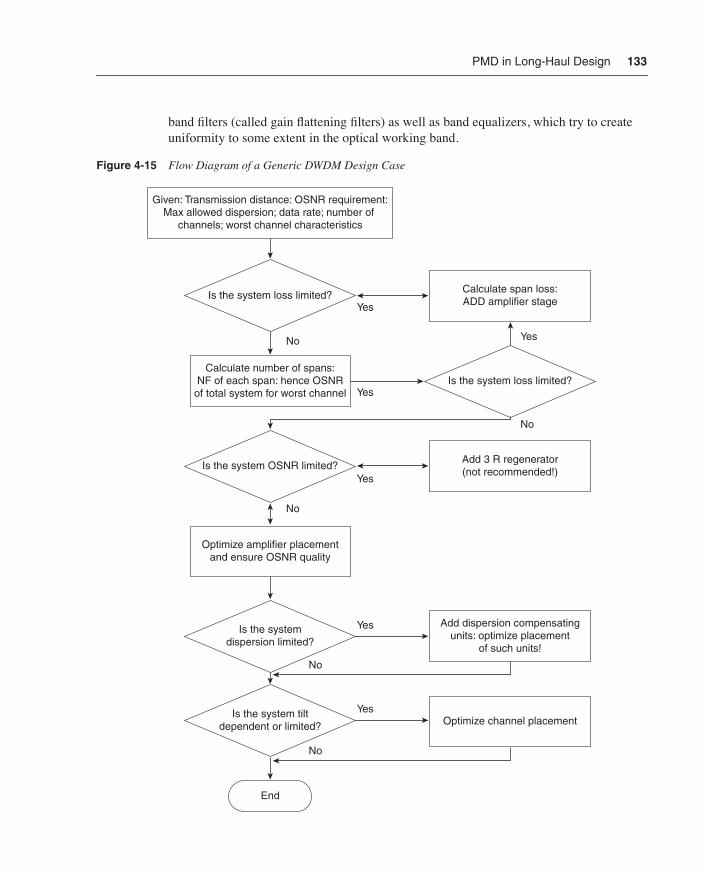
Figure 4-15 shows the basic flow diagram that we would use to design an optical network based on system design principles explained so far. One issue that has not been discussed is the tilt limited system, whereby the gain of the amplifier produces different amplification for different channels (and hence different noise levels), generating different values of OSNR for different channels. Compensating tilt is a hard task despite the availability of flat
DGD = (PMD Coefficient) Length
12---
×
DGD 2 ps Km 2∗ 625 2∗25 50 ps= = = =
0749.book Page 132 Monday, November 11, 2002 10:28 AM
PMD in Long-Haul Design 133
band filters (called gain flattening filters) as well as band equalizers, which try to create uniformity to some extent in the optical working band.
Figure 4-15 Flow Diagram of a Generic DWDM Design Case
0749.book Page 133 Monday, November 11, 2002 10:28 AM

134 Chapter 4: WDM Network Design -1
ExamplesThe following case studies reinforce the principles discussed so far in this chapter.
Case 1Design a 4 ×25 span WDM link with an optical amplifier gain of 22 dB and NF equal to 5 dB.
Calculate the final OSNR if the input power is 0 dB. Calculate the signal power at the receiver.
Will this system work if the receiver sensitivity is a minimum of –25 dB?
Will the system work if the input power is 10 dB?
The answer is shown in Figure 4-16.
Figure 4-16 Answer to the Problem
You can use one of the two methods to determine the final OSNR.
Method 1OSNRFinal = P0 + 58 – –10logN – NF
N = 4 (number of spans)
NF = 5
=25 dB
OSNRFinal = 0 + 58 – 25 –10log4 –5
= 58 – 25 – 6 – 5 = 22 dB (the best estimate value)
Method 2 OSNR stage by stage analysis using the formula:
OSNRstagei = 1/(1/OSNRstage0 + NF.h.v.∆f /Pin) (1/OSNRstage0 = 0)
0749.book Page 134 Monday, November 11, 2002 10:28 AM

Examples 135
OSNR Stage 1
NF = 5 dB converting to linear = 3.166 (10NF dB/10)
h = Plank’s constant = 6.6260E – 34
v = frequency of light 1.9350E + 14
∆f = bandwidth (measuring the NF) = 12.5 KHz (.1 nm)
Pin = input power at the amplifier
0 – 25 dB = –25 dB
OSNRstage1 = 28 dB
Output from the amplifier = –25 + 22 = –3 dB
OSNR Stage 2
OSNRstage2 = 1/(1/OSNRstage1 + NF.h.v.∆f /Pin)
Input at the second amplifier
= –3 – 25 = –28 dB
OSNRstage2 = 23 dB
Output from the amplifier = –28 + 22 = –6
OSNR Stage 3
OSNRstage3 =1/(1/OSNRstage3 + NF.h.v.∆f /Pin)
Input at the third amplifier = –6 – 25 = –31 dB
OSNRstage3 = 20 dB
Output from the amplifier = –31 + 22 = –9 dB
Power at the receiver
= –9 – 25 = –34 dB
If the receiver sensitivity is –25, the system will not work.
The solution is to (a) increase the gain of the amplifier (b) increase the input power of the transmitter.
The same solution for 10dB input power is shown in Figure 4-16.
Using Method 1: OSNRfinal = 10 + 58 – 25 – 6 – 5 = 32
Method 2: gives OSNRfinal = 29 dB
The difference in value is due to the approximation made in the parameters.
0749.book Page 135 Monday, November 11, 2002 10:28 AM

136 Chapter 4: WDM Network Design -1
Final power at the receiver
= 10(Tr) – 25 (loss1) + 22 (gain1) – 25 (loss2) + 22 (gain 2) – 25 (loss 3) + 22 (gain 3) – 25 (loss) = –24 dB
The receiver sensitivity is given as –25 dB, so the system will work.
Case 2Calculate the number of spans in this link, given Pin = 0 dB; OSNRfinal = 20 dB total length = 300 km Bit rate = 5 Gbps; NF = 5 dB. (Assume fiber type is SMF ∝ = .2 dB/km)
AnswerTotal loss over entire length = 300 × 0.2 = 60 dB
Attenuation per span = 60/N (assume N number of spans
OSNRFinal = P0 + 58 – –10logN – NF
20 = 0 + 58 – 60/N –10logN – 5
-33 = –60/N – 10logN
Rearranging, you get this:
60/N – 10logN = 33
Solving for N (for N = 2)
60/2 + 10log2 = 33
Therefore, the number of spans = 2.
Case 3OSNR = 20 dB, dispersion of the fiber is 17 ps/nm-km, span loss = 22 dB.
What is the total length of the system? (NF of the amplifier = 4 dB, and dispersion tolerance is given as 1600 ps/nm, Pin = 10)
AnswerOSNRFinal = P0 + 58 – –10logN – NF
20 = 10 + 58 – 22 – 4 – 10logN
0749.book Page 136 Monday, November 11, 2002 10:28 AM

Examples 137
–22 = –10 logN
N = 158 spans
Therefore, total length = 158 * 22/0.2 = 17,280 km (theoretical limit)
But due to dispersion, max length = 1600 ps.nm/17 ps /nm.km = 94 km.
Case 4Customer A wants to build a 200 km OC48 link to transport traffic. Design the link with the following parameters. (Assume SMF-28 fiber with α = .25 dB/km/ and 18 ps/nm/km as the dispersion characteristic.)
Receiver sensitivity: –18 dBm @BER=e-12
Receiver overload: –10 dBm @BER=e-12
Transmit power: +7 to +9 dBm
Dispersion tolerance: 1500 ps/nm
Dispersion penalty: 1.5 dB @ 1500 ps/nm
OSNR tolerance: 20 dB @ Resolution Bandwidth 0.1 nm
EDFA
Input power range: +3 to –25 dBm; Gain: 20 dB to 14 dB
Maximum output power: +17 dBm; Noise Figure: 5 dB
DCU
Loss 5 dB, dispersion compensation –1100 ps
AnswerThe answer requires several steps. Refer to Figure 4-17.
Figure 4-17 Case 4 Answer
0749.book Page 137 Monday, November 11, 2002 10:28 AM
138 Chapter 4: WDM Network Design -1
Step 1 The total distance is 200 km; therefore, total loss is 200 * .25 = 50 dB. You need amplifiers to reach that distances.
Step 2 Total dispersion is 200 km * 18 ps.nm / km = 3600 ps.nm
You need to use dispersion compensators because the given dispersion tolerance is 1500 ps.nm. The maximum distance for this system without DCU is 1500/18 = 83.33 km given DCU = –1100 ps. If you strategically place 3 DCU, you get (3600 – 3 * 1100) = 300 ps, which is well within the limit. The DCU has a 5 dB passthrough loss, so it is best to place it before preamplifiers.
Analysis of the problem
Transmit power = + 7 dB
Stage 1:
loss = –10 (link loss) – 6 (DCU loss) – 1.5 (margin) = –17.5 dB
Pin = Power at the end of stage 1 = 7 – 17.5 = –10.5 dB
Stage 1 amplifier gain: 20
Power output from the amplifier: (power input + gain) – 10.5 dB + 20 = 9.5 dB
OSNR calculation
OSNRstagei =1/(1/OSNR0 + NF.h.v.∆f /Pin) (for stage 1 1/OSNR0 = 0)
OSNR1 = Pin/NF.h.v. ∆f
Substituting the values Pin = –10.5 dB = 8.9125E – 05 W (convert to watts)
NF = 5 dB converting to linear = 3.166 (10NF dB/10)
h = planks constant = 6.6260E – 34
v = frequency of light 1.9350E + 14
∆f = bandwidth (measuring the NF) = 12.5 KHz (.1 nm)
Substituting, you get OSNR = 42 dB
Stage 2:
Loss = –20 (link loss – 6 (DCU loss) – 1.5 (margin) = –27.5 dB
Power at the end of stage 2
Pin = 9.5 – 20 – 6 – 1.5 (margin) = –18 dB
Stage 2 amplifier gain: 20
0749.book Page 138 Monday, November 11, 2002 10:28 AM
Examples 139
Power output from amplifier: –18 + 20 = 2 dB
OSNRstage2 = 1/(1/OSNR1 + NF.h.v.∆f /Pin)
OSNR1 is the OSNR of stage 1 = 42 dB and Pin = –18 dB
OSNRstage 2 = 34 dB
Stage 3 loss:
–20(link loss) – 6 (DCU loss) – 1.5 (margin) = –27.5 dB (loss)
Power at the end of stage 3
Pin= 2 – 27.5 = –25.5 dB
Stage 3 amplifier gain 20 dB
Power output from the amplifier: = –25.5 + 20 = –5.5 dB
OSNR
OSNRstage3 = 1/(1/OSNRstage2 + NF.h.v.Df /Pin)
OSNR = 26
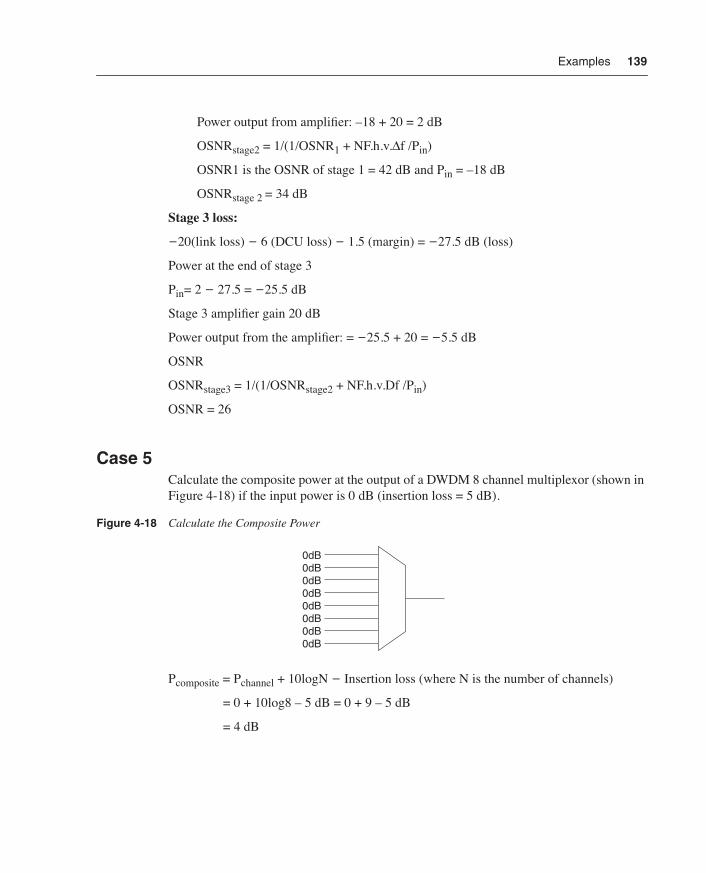
Case 5Calculate the composite power at the output of a DWDM 8 channel multiplexor (shown in Figure 4-18) if the input power is 0 dB (insertion loss = 5 dB).
Figure 4-18 Calculate the Composite Power
Pcomposite = Pchannel + 10logN – Insertion loss (where N is the number of channels)
= 0 + 10log8 – 5 dB = 0 + 9 – 5 dB
= 4 dB
0749.book Page 139 Monday, November 11, 2002 10:28 AM

140 Chapter 4: WDM Network Design -1
ExercisesThe following exercises are left for you to solve. Use previous examples as guidelines.
1 Calculate the dispersion and the receiver power of an optical link that is 90 km in length. The transmit power = +8 dB, the receiver sensitivity = –18 dB, and the dispersion tolerance = 1500 ps/nm (SMF ∝ = .25 dB/km 18 ps/nm-km). Is it dispersion limited? Design the link for proper network operation if you need to use EDFA 15 dB (gain) and DCU –1100 ps and 5 dB loss).
2 Design a 4 × 25 span WDM link with optical amplifier gain = 18 dB and NF = 6 dB.
Calculate final OSNR if the input power is 0 dB. Calculate signal power at the receiver.
(The receiver sensitivity is –25 dB at BER 10-15). Does the system work?
Now calculate the final OSNR by replacing the following:
— The transmitter with input power to +7 dB
— The amplifier gain to 22 dB
3 Calculate power in milliwatts if the input power were 0 dBm.
Calculate the power in dBm if the input power were 12 mW.
Hint: XmW power is 10 * log10(x) in dBm
Y dBm power is 10Y/10 in mW
4 Calculate the composite power at the output of a DWDM 16-channel mux if the input power is 4 dB. If the input is plugged into an amplifier, how much attenuation do you need (given NF = 5 dB, input range = 0–25 dB, gain = 22)
SummaryThis chapter discussed optical network system-level designs. We initially considered power budget-based design, from which we migrate to more complex OSNR-based designs. This chapter showed the importance of OSNR in estimating BER and the need for evaluation of the Q-factor as an intermediate stage in BER development. We discuss dispersion-based systems and penalties that are associated with dispersion-limited systems. We show how dispersion-limited systems can be compensated using generic schemes and hence show the methods of pre- and postcompensation as well as placement of such compensating units. Nonlinear effects are also studied from a design point of view, as well as the various penalties and their cures from a system design perspective. Finally, we analyzed numerical examples for the studied system design principles.
0749.book Page 140 Monday, November 11, 2002 10:28 AM
References 141
References1 Bononi, A. Optical Networking. Springer Publishers, 1999.
2 Senior, J., C. Qiao, and S. Dixit. All Optical Networking 1999: Architecture, Control and Management Issues. Proceedings SPIE, 2000.
3 Agrawal, Govind P. Fiber-Optic Communication Systems, Second Edition. Wiley Interscience, 1997.
4 Keiser, G. Optical Fiber Communications, Third Edition. McGraw-Hill, 2000.
5 Mukherjee, B. Optical Communications Networks. McGraw-Hill, 1997.
6 Green, P. Fiber Optics Networks. Prentice Hall, 1992.
7 Ramaswami, R. and K. Sivarajan. Optical Network: A Practical Perspective, Second Edition. Morgan Kaufmann, 2001.
8 Agarwal, G. Nonlinear Fiber Optics, Second Edition. Academic Press, 1995.
9 Saleh, B. and M. Teich. Fundamentals of Photonics. Wiley, 1991.
10 Ramamurthiu, B. Design of Optical WDM Networks, LAN, MAN, and WAN Architectures. Kluwer, 2001.
0749.book Page 141 Monday, November 11, 2002 10:28 AM