Embed Size (px)
Citation preview

W-1
C h a p t e r 3 / The Structure ofCrystalline Solids
3.16W X-RAY DIFFRACTION: DETERMINATION OF
CRYSTAL STRUCTURES
Historically, much of our understanding regarding the atomic and moleculararrangements in solids has resulted from x-ray diffraction investigations; further-more, x-rays are still very important in developing new materials. We will now givea brief overview of the diffraction phenomenon and how, using x-rays, atomicinterplanar distances and crystal structures are deduced.
THE DIFFRACTION PHENOMENONDiffraction occurs when a wave encounters a series of regularly spaced obstaclesthat (1) are capable of scattering the wave, and (2) have spacings that are compa-rable in magnitude to the wavelength. Furthermore, diffraction is a consequence ofspecific phase relationships established between two or more waves that have beenscattered by the obstacles.
Consider waves 1 and 2 in Figure 3.1aW which have the same wavelength (�)and are in phase at point O–O�. Now let us suppose that both waves are scatteredin such a way that they traverse different paths. The phase relationship between thescattered waves, which will depend upon the difference in path length, is important.One possibility results when this path length difference is an integral number ofwavelengths. As noted in Figure 3.1aW, these scattered waves (now labeled 1� and2�) are still in phase. They are said to mutually reinforce (or constructively inter-fere with) one another; and, when amplitudes are added, the wave shown on theright side of the figure results. This is a manifestation of diffraction, and we referto a diffracted beam as one composed of a large number of scattered waves thatmutually reinforce one another.
Other phase relationships are possible between scattered waves that will notlead to this mutual reinforcement.The other extreme is that demonstrated in Figure3.1bW, wherein the path length difference after scattering is some integral numberof half wavelengths. The scattered waves are out of phase—that is, correspondingamplitudes cancel or annul one another, or destructively interfere (i.e., the result-ant wave has zero amplitude), as indicated on the extreme right side of the figure.Of course, phase relationships intermediate between these two extremes exist,resulting in only partial reinforcement.
X-RAY DIFFRACTION AND BRAGG’S LAWX-rays are a form of electromagnetic radiation that have high energies and shortwavelengths—wavelengths on the order of the atomic spacings for solids. When abeam of x-rays impinges on a solid material, a portion of this beam will be scat-tered in all directions by the electrons associated with each atom or ion that lies
wc03.16.qxd 05/16/2002 11:48 AM Page 1

W-2
within the beam’s path. Let us now examine the necessary conditions for diffrac-tion of x-rays by a periodic arrangement of atoms.
Consider the two parallel planes of atoms A–A� and B–B� in Figure 3.2W, whichhave the same h, k, and l Miller indices and are separated by the interplanar spacingdhkl. Now assume that a parallel, monochromatic, and coherent (in-phase) beam of
FIGURE 3.2WDiffraction of x-rays byplanes of atoms (A–A�
and B–B�).
� �
��
�
�
Incidentbeam
Diffractedbeam
P
S T
Q
A
B
1
2
A'
B'
1'
2'
dhkl
FIGURE 3.1W(a) Demonstration of
how two waves (labeled1 and 2) that have the
same wavelength � andremain in phase after ascattering event (waves
1� and 2�) constructivelyinterfere with one
another. The amplitudesof the scattered waves
add together in theresultant wave.
(b) Demonstration ofhow two waves (labeled
3 and 4) that have thesame wavelength andbecome out of phase
after a scattering event(waves 3� and 4�)
destructively interferewith one another. Theamplitudes of the two
scattered waves cancelone another.
Wave 1 Wave 1'
Wave 2
Position
Wave 2'
+
Scatteringevent
Am
plit
ude
O
(a)
(b)
O'
A
� �
A
A
A
� �
�
2A
Wave 3 Wave 3'
Wave 4
Position
Wave 4'
+
Scatteringevent
Am
plit
ude
P
P'
A
� �
A
A
A
�
�
wc03.16.qxd 05/16/2002 11:48 AM Page 2

W-3
x-rays of wavelength � is incident on these two planes at an angle �. Two rays inthis beam, labeled 1 and 2, are scattered by atoms P and Q. Constructive interfer-ence of the scattered rays 1� and 2� occurs also at an angle � to the planes, if thepath length difference between 1–P–1� and 2–Q–2� (i.e., ) is equal to awhole number, n, of wavelengths. That is, the condition for diffraction is
(3.1W)
or
(3.2W)
Equation 3.2W is known as Bragg’s law; also, n is the order of reflection, whichmay be any integer (1, 2, 3, . . . ) consistent with sin � not exceeding unity.Thus, we havea simple expression relating the x-ray wavelength and interatomic spacing to the an-gle of the diffracted beam. If Bragg’s law is not satisfied, then the interference willbe nonconstructive in nature so as to yield a very low-intensity diffracted beam.
The magnitude of the distance between two adjacent and parallel planes ofatoms (i.e., the interplanar spacing dhkl) is a function of the Miller indices (h, k, andl) as well as the lattice parameter(s). For example, for crystal structures that havecubic symmetry,
(3.3W)
in which a is the lattice parameter (unit cell edge length). Relationships similar toEquation 3.3W, but more complex, exist for the other six crystal systems noted inTable 3.2.
Bragg’s law, Equation 3.2W, is a necessary but not sufficient condition for dif-fraction by real crystals. It specifies when diffraction will occur for unit cells havingatoms positioned only at cell corners. However, atoms situated at other sites (e.g., faceand interior unit cell positions as with FCC and BCC) act as extra scattering centers,which can produce out-of-phase scattering at certain Bragg angles. The net result isthe absence of some diffracted beams that, according to Equation 3.2W, should bepresent. For example, for the BCC crystal structure, h � k � l must be even if dif-fraction is to occur, whereas for FCC, h, k, and l must all be either odd or even.
DIFFRACTION TECHNIQUESOne common diffraction technique employs a powdered or polycrystalline speci-men consisting of many fine and randomly oriented particles that are exposed tomonochromatic x-radiation. Each powder particle (or grain) is a crystal, and hav-ing a large number of them with random orientations ensures that some particlesare properly oriented such that every possible set of crystallographic planes will beavailable for diffraction.
The diffractometer is an apparatus used to determine the angles at whichdiffraction occurs for powdered specimens; its features are represented schemati-cally in Figure 3.3W. A specimen S in the form of a flat plate is supported so thatrotations about the axis labeled O are possible; this axis is perpendicular to theplane of the page. The monochromatic x-ray beam is generated at point T, and
dhkl �a2h2 � k2 � l
2
� 2dhkl sin u
nl � dhkl sin u � dhkl sin u
nl � SQ � QT
SQ � QT
wc03.16.qxd 05/16/2002 11:48 AM Page 3

W-4
the intensities of diffracted beams are detected with a counter labeled C in thefigure. The specimen, x-ray source, and counter are all coplanar.
The counter is mounted on a movable carriage that may also be rotated aboutthe O axis; its angular position in terms of 2� is marked on a graduated scale.2
Carriage and specimen are mechanically coupled such that a rotation of the speci-men through � is accompanied by a 2� rotation of the counter; this assures that theincident and reflection angles are maintained equal to one another (Figure 3.3W).Collimators are incorporated within the beam path to produce a well-defined andfocused beam. Utilization of a filter provides a near-monochromatic beam.
As the counter moves at constant angular velocity, a recorder automaticallyplots the diffracted beam intensity (monitored by the counter) as a function of 2�;2� is termed the diffraction angle, which is measured experimentally. Figure 3.4Wshows a diffraction pattern for a powdered specimen of lead. The high-intensitypeaks result when the Bragg diffraction condition is satisfied by some set of crys-tallographic planes. These peaks are plane-indexed in the figure.
Other powder techniques have been devised wherein diffracted beam intensityand position are recorded on a photographic film instead of being measured by acounter.
FIGURE 3.3W Schematic diagram of anx-ray diffractometer; T � x-ray source,S � specimen, C � detector, and O �the axis around which the specimen anddetector rotate.
FIGURE 3.4W Diffraction pattern for powdered lead. (Courtesy of WesleyL. Holman.)
O
�
2�
S
T
C
160°
140°
120°
100°80°
60°
40°
20°0°
Inte
nsit
y
0.0 10.0 20.0 30.0 40.0
(111)
(200)(220)
(311)(222)
(400) (331) (420) (422)
50.0
Diffraction angle 2�
60.0 70.0 80.0 90.0 100.0
2 Note that the symbol � has been used in two different contexts for this discussion. Here,� represents the angular locations of both x-ray source and counter relative to the speci-men surface. Previously (e.g., Equation 3.2W), it denoted the angle at which the Bragg cri-terion for diffraction is satisfied.
wc03.16.qxd 05/16/2002 11:48 AM Page 4

W-5
One of the primary uses of x-ray diffractometry is for the determination of crys-tal structure. The unit cell size and geometry may be resolved from the angularpositions of the diffraction peaks, whereas arrangement of atoms within the unitcell is associated with the relative intensities of these peaks.
X-rays, as well as electron and neutron beams, are also used in other types ofmaterial investigations. For example, crystallographic orientations of single crys-tals are possible using x-ray diffraction (or Laue) photographs. On page 31 isshown a photograph that was generated using an incident electron beam that wasdirected on a gallium arsenide crystal; each spot (with the exception of the bright-est one near the center) resulted from an electron beam that was diffracted by aspecific set of crystallographic planes. Other uses of x-rays include qualitative andquantitative chemical identifications and the determination of residual stressesand crystal size.
EXAMPLE PROBLEM 3.1W
For BCC iron, compute (a) the interplanar spacing, and (b) the diffraction anglefor the (220) set of planes. The lattice parameter for Fe is 0.2866 nm (2.866 Å).Also, assume that monochromatic radiation having a wavelength of 0.1790 nm(1.790 Å) is used, and the order of reflection is 1.
SOLUTION
(a) The value of the interplanar spacing dhkl is determined using Equation 3.3W,with a � 0.2866 nm, and h � 2, k � 2, and l � 0, since we are considering the(220) planes. Therefore,
(b) The value of � may now be computed using Equation 3.2W, with n � 1,since this is a first-order reflection:
The diffraction angle is 2�, or
2u � 122 162.13�2 � 124.26�
u � sin�110.8842 � 62.13�
sin u �nl
2dhkl�112 10.1790 nm2
122 10.1013 nm2� 0.884
�0.2866 nm21222 � 1222 � 1022
� 0.1013 nm 11.013 Å2
dhkl � a2h2 � k2 � l
2
wc03.16.qxd 05/16/2002 11:48 AM Page 5

W-6
7.7W DEFORMATION BY TWINNING
In addition to slip, plastic deformation in some metallic materials can occur bythe formation of mechanical twins, or twinning. The concept of a twin was intro-duced in Section 4.6; that is, a shear force can produce atomic displacements suchthat on one side of a plane (the twin boundary), atoms are located in mirror-imagepositions of atoms on the other side. The manner in which this is accomplished isdemonstrated in Figure 7.1W. Here, open circles represent atoms that did notmove, and dashed and solid circles represent original and final positions, respec-tively, of atoms within the twinned region. As may be noted in this figure, the dis-placement magnitude within the twin region (indicated by arrows) is proportionalto the distance from the twin plane. Furthermore, twinning occurs on a definitecrystallographic plane and in a specific direction that depend on crystal structure.For example, for BCC metals, the twin plane and direction are (112) and [111],respectively.
Slip and twinning deformations are compared in Figure 7.2W for a single crys-tal that is subjected to a shear stress �. Slip ledges are shown in Figure 7.2aW, theformation of which were described in Section 7.5; for twinning, the shear deforma-tion is homogeneous (Figure 7.2bW). These two processes differ from one anotherin several respects. First, for slip, the crystallographic orientation above and below
FIGURE 7.1W Schematic diagram showing how twinning results from an appliedshear stress �. In (b), open circles represent atoms that did not change position;dashed and solid circles represent original and final atom positions, respectively.(From G. E. Dieter, Mechanical Metallurgy, 3rd edition. Copyright © 1986 byMcGraw-Hill Book Company, New York. Reproduced with permission ofMcGraw-Hill Book Company.)
Twin plane
Polished surface
Twin plane
(a)
τ
τ
(b)
C h a p t e r 7 / Dislocations andStrengthening Mechanisms
wc07.7.qxd 05/16/2002 11:50 AM Page 6

W-7
the slip plane is the same both before and after the deformation; for twinning, therewill be a reorientation across the twin plane. In addition, slip occurs in distinct atomicspacing multiples, whereas the atomic displacement for twinning is less than theinteratomic separation.
Mechanical twinning occurs in metals that have BCC and HCP crystal struc-tures, at low temperatures, and at high rates of loading (shock loading), conditionsunder which the slip process is restricted; that is, there are few operable slip systems.The amount of bulk plastic deformation from twinning is normally small relativeto that resulting from slip. However, the real importance of twinning lies with theaccompanying crystallographic reorientations; twinning may place new slip systemsin orientations that are favorable relative to the stress axis such that the slip processcan now take place.
FIGURE 7.2W For a singlecrystal subjected to a shearstress �, (a) deformation byslip; (b) deformation bytwinning.
(a) (b)
� �
� �
Slipplanes
Twin
Twinplanes
wc07.7.qxd 05/16/2002 11:50 AM Page 7

W-8
C h a p t e r 8 / Failure
8.5W PRINCIPLES OF FRACTURE MECHANICS
(DETAILED VERSION)Brittle fracture of normally ductile materials, such as that shown in the chapter-opening photograph of this chapter in the text, has demonstrated the need for abetter understanding of the mechanisms of fracture. Extensive research endeavorsover the past several decades have led to the evolution of the field of fracture me-chanics. This subject allows quantification of the relationships between materialproperties, stress level, the presence of crack-producing flaws, and crack propaga-tion mechanisms. Design engineers are now better equipped to anticipate, andthus prevent, structural failures. The present discussion centers on some of thefundamental principles of the mechanics of fracture.
STRESS CONCENTRATIONThe fracture strength of a solid material is a function of the cohesive forces thatexist between atoms. On this basis, the theoretical cohesive strength of a brittle elas-tic solid has been estimated to be approximately E�10, where E is the modulus ofelasticity. The experimental fracture strengths of most engineering materials nor-mally lie between 10 and 1000 times below this theoretical value. In the 1920s, A.A. Griffith proposed that this discrepancy between theoretical cohesive strengthand observed fracture strength could be explained by the presence of very small,microscopic flaws or cracks that always exist under normal conditions at the sur-face and within the interior of a body of material. These flaws are a detriment tothe fracture strength because an applied stress may be amplified or concentratedat the tip, with the magnitude of this amplification depending on crack orientationand geometry. This phenomenon is demonstrated in Figure 8.1W, a stress profileacross a cross section containing an internal crack. As indicated by this profile, themagnitude of this localized stress diminishes with distance away from the crack tip.At positions far removed, the stress is equal to the nominal stress �0, or the appliedload divided by the specimen cross-sectional area (perpendicular to this load). Dueto their ability to amplify an applied stress in their locale, these flaws are sometimescalled stress raisers.
If it is assumed that a crack is similar to an elliptical hole through a plate andis oriented perpendicular to the applied stress, the maximum stress, �m, at the cracktip is equal to
(8.1W)
where �0 is the magnitude of the nominal applied tensile stress, �t is the radius ofcurvature of the crack tip (Figure 8.1aW), and a represents the length of a surface
sm � s0 c1 � 2 a artb1�2 d
wc08.5.qxd 05/16/2002 11:56 AM Page 8

W-9
FIGURE 8.1W (a) The geometry of surface and internal cracks. (b) Schematicstress profile along the line X–X� in (a), demonstrating stress amplification atcrack tip positions.
ρt
σ0
σ0
X'X
x'x2a
a
Position along X–X'
(b)
σ0
σm
Str
ess
x'x
(a)
crack, or half of the length of an internal crack. For a relatively long microcrackthat has a small tip radius of curvature, the factor (a��t)
1�2 may be very large (cer-tainly much greater than unity); under these circumstances Equation 8.1W takesthe form
(8.2W)
Furthermore, �m will be many times the value of �0.Sometimes the ratio �m��0 is denoted as the stress concentration factor Kt:
(8.3W)
which is simply a measure of the degree to which an external stress is amplified atthe tip of a crack.
Note that stress amplification is not restricted to these microscopic defects; itmay occur at macroscopic internal discontinuities (e.g., voids), at sharp corners, andat notches in large structures. Figure 8.2W shows theoretical stress concentrationfactor curves for several simple and common macroscopic discontinuities.
Furthermore, the effect of a stress raiser is more significant in brittle than inductile materials. For a ductile material, plastic deformation ensues when themaximum stress exceeds the yield strength. This leads to a more uniform distri-bution of stress in the vicinity of the stress raiser and to the development of amaximum stress concentration factor less than the theoretical value. Such yield-ing and stress redistribution do not occur to any appreciable extent around flaws
Kt �sm
s0� 2 a a
rtb1� 2
sm � 2s0 a artb1�2
wc08.5.qxd 05/16/2002 11:56 AM Page 9

W-10
and discontinuities in brittle materials; therefore, essentially the theoretical stressconcentration will result.
Griffith then went on to propose that all brittle materials contain a populationof small cracks and flaws that have a variety of sizes, geometries, and orientations.Fracture will result when, upon application of a tensile stress, the theoretical cohe-sive strength of the material is exceeded at the tip of one of these flaws. This leadsto the formation of a crack that then rapidly propagates. If no flaws were present,
FIGURE 8.2WTheoretical stress
concentration factorcurves for three simple
geometrical shapes.(From G. H.
Neugebauer, Prod.Eng. NY), Vol. 14,
pp. 82–87, 1943.) dw
Str
ess
conc
entr
atio
nfa
ctor
Kt
0 0.2 0.4 0.6 0.8 1.01.8
2.2
2.6
3.0
3.4
(a)
(b)
(c)
d
w
h
b
2r
b
w
rh
rh
br
12
br
wh
= 2.00
= 1
br = 4
=
wh
= 1.25
wh
= 1.10
Str
ess
conc
entr
atio
n fa
ctor
Kt
0 0.2 0.4 0.6 0.81.0
1.4
1.8
2.2
2.6
3.0
3.4
3.8
w
h
r
Str
ess
conc
entr
atio
n fa
ctor
Kt
0 0.2 0.4 0.6 0.8 1.0
1.2
1.4
1.6
1.8
2.0
2.2
2.4
2.6
2.8
3.0
3.2
1.0
wc08.5.qxd 05/16/2002 11:56 AM Page 10

W-11
the fracture strength would be equal to the cohesive strength of the material. Verysmall and virtually defect-free metallic and ceramic whiskers have been grown withfracture strengths that approach their theoretical values.
GRIFFITH THEORY OF BRITTLE FRACTUREDuring the propagation of a crack, there is a release of what is termed the elasticstrain energy, some of the energy that is stored in the material as it is elastically de-formed. Furthermore, during the crack extension process, new free surfaces are cre-ated at the faces of a crack, which give rise to an increase in surface energy of thesystem. Griffith developed a criterion for crack propagation of an elliptical crack(Figure 8.1aW) by performing an energy balance using these two energies. Hedemonstrated that the critical stress �c required for crack propagation in a brittlematerial is described by
(8.4W)
where
E � modulus of elasticity
�s � specific surface energy
a � one half the length of an internal crack
Worth noting is that this expression does not involve the crack tip radius �t, as doesthe stress concentration equation (Equation 8.1W); however, it is assumed that theradius is sufficiently sharp (on the order of the interatomic spacing) so as to raisethe local stress at the tip above the cohesive strength of the material.
The previous development applies only to completely brittle materials, for whichthere is no plastic deformation. Most metals and many polymers do experience someplastic deformation during fracture; thus, crack extension involves more thanproducing just an increase in the surface energy. This complication may be accom-modated by replacing �s in Equation 8.4W by �s � �p, where �p represents a plas-tic deformation energy associated with crack extension. Thus,
(8.5W)
For highly ductile materials, it may be the case that such that
(8.6W)
In the 1950s, G. R. Irwin chose to incorporate both �s and �p into a single term,as
(8.7W)
is known as the critical strain energy release rate. Incorporation of Equation 8.7Winto Equation 8.5W after some rearrangement leads to another expression for thegc
gc � 21gs � gp2gc,
sc � a2Egp
pab1� 2
gp W gs
sc � c 2E 1gs � gp2pa
d 1� 2
sc � a2Egs
pab1� 2
wc08.5.qxd 05/16/2002 11:56 AM Page 11

W-12
(a) (b) (c)
FIGURE 8.3W Thethree modes of cracksurface displacement.
(a) Mode I, opening ortensile mode; (b) mode
II, sliding mode; and(c) mode III, tearing
mode.
Griffith cracking criterion as
(8.8W)
Thus, crack extension occurs when ��2a�E exceeds the value of for the partic-ular material under consideration.
EXAMPLE PROBLEM 8.1W
A relatively large plate of a glass is subjected to a tensile stress of 40 MPa. Ifthe specific surface energy and modulus of elasticity for this glass are 0.3 J/m2
and 69 GPa, respectively, determine the maximum length of a surface flaw thatis possible without fracture.
SOLUTION
To solve this problem it is necessary to employ Equation 8.4W. Rearrangementof this expression such that a is the dependent variable, and realizing that
and E � 69 GPa, leads to
STRESS ANALYSIS OF CRACKSAs we continue to explore the development of fracture mechanics, it is worthwhileto examine the stress distributions in the vicinity of the tip of an advancing crack.There are three fundamental ways, or modes, by which a load can operate on acrack, and each will affect a different crack surface displacement; these are illus-trated in Figure 8.3W. Mode I is an opening (or tensile) mode, whereas modes IIand III are sliding and tearing modes, respectively. Mode I is encountered most fre-quently, and only it will be treated in the ensuing discussion on fracture mechanics.
� 8.2 � 10�6 m � 0.0082 mm � 8.2 mm
�122 169 � 109 N/m22 10.3 N/m2
p140 � 106 N/m222
a �2Egs
ps2
s � 40 MPa, gs � 0.3 J/m2,
gc
gc �ps2a
E
wc08.5.qxd 05/16/2002 11:56 AM Page 12

W-13
1 This �y denotes a tensile stress parallel to the y-direction, and should not be confusedwith the yield strength (Section 6.6), which uses the same symbol.2 The f(�) functions are as follows:
f xy1u2 � sin u
2 cos u
2 cos
3u2
f y1u2 � cos u
2 a1 � sin
u
2 sin
3u2b
fx1u2 � cos u
2 a1 � sin
u
2 sin
3u2b
y
x
z
r
�xy �y
�x
�z
�
FIGURE 8.4W The stresses actingin front of a crack that is loadedin a tensile mode I configuration.
For this mode I configuration, the stresses acting on an element of material areshown in Figure 8.4W. Using elastic theory principles and the notation indicated,tensile (�x and �y)1 and shear (�xy) stresses are functions of both radial distance rand the angle � as follows:2
(8.9aW)
(8.9bW)
(8.9cW)
If the plate is thin relative to the dimensions of the crack, then �z � 0, or a condi-tion of plane stress is said to exist. At the other extreme (a relatively thick plate),�z � �(�x � �y), and the state is referred to as plane strain (since z � 0); � in thisexpression is Poisson’s ratio.
txy �K12pr
fxy 1u2
sy �K12pr
fy 1u2
sx �K12pr
fx 1u2
wc08.5.qxd 05/16/2002 11:56 AM Page 13

W-14
2a a
(a) (b)
FIGURE 8.5W Schematicrepresentations of (a) aninterior crack in a plate ofinfinite width, and (b) anedge crack in a plate ofsemi-infinite width.
In Equations 8.9W, the parameter K is termed the stress intensity factor; its useprovides for a convenient specification of the stress distribution around a flaw. Notethat this stress intensity factor and the stress concentration factor Kt in Equation8.3W, although similar, are not equivalent.
The stress intensity factor is related to the applied stress and the crack lengthby the following equation:
(8.10W)
Here Y is a dimensionless parameter or function that depends on both the crackand specimen sizes and geometries, as well as the manner of load application. Morewill be said about Y in the discussion that follows. Moreover, note that K has theunusual units of MPa (psi [alternatively ksi ]).
FRACTURE TOUGHNESSIn the previous discussion, a criterion was developed for the crack propagation ina brittle material containing a flaw; fracture occurs when the applied stress levelexceeds some critical value �c (Equation 8.4W). Similarly, since the stresses inthe vicinity of a crack tip can be defined in terms of the stress intensity factor, acritical value of K exists that may be used to specify the conditions for brittle frac-ture; this critical value is termed the fracture toughness Kc, and, from Equation 8.10W,is defined by
(8.11W)
Here �c again is the critical stress for crack propagation, and we now represent Yas a function of both crack length (a) and component width (W)—that is, as Y(a�W).
Relative to this Y(a�W) function, as the a�W ratio approaches zero (i.e., for verywide planes and short cracks), Y(a�W) approaches a value of unity. For example, fora plate of infinite width having a through-thickness crack, Figure 8.5aW, Y(a�W) �1.0; for a plate of semi-infinite width containing an edge crack of length a (Figure8.5bW), Y(a�W) � 1.1. Mathematical expressions for Y(a�W) (often relatively
Kc � Y1a�W2sc1pa
1in.1in.1m
K � Ys1pa
wc08.5.qxd 05/16/2002 11:56 AM Page 14

W-15
B
W
�
�
2a
W2
FIGURE 8.6W Schematic representation of a flat plate of finitewidth having a through-thickness center crack.
complex) in terms of a�W are required for components of finite dimensions. Forexample, for a center-cracked (through-thickness) plate of width W (Figure 8.6W)
(8.12W)
Here the �a�W argument for the tangent is expressed in radians, not degrees. It isoften the case for some specific component-crack configuration that Y(a�W) is plot-ted versus a�W (or some variation of a�W). Several of these plots are shown inFigures 8.7aW, bW, and cW; included in the figures are equations that are used todetermine Kcs.
By definition, fracture toughness is a property that is the measure of a mater-ial’s resistance to brittle fracture when a crack is present. Its units are the same asfor the stress intensity factor (i.e., or ).
For relatively thin specimens, the value of Kc will depend on and decrease withincreasing specimen thickness B, as indicated in Figure 8.8W. Eventually, Kc be-comes independent of B, at which time the condition of plane strain is said to exist.3
The constant Kc value for thicker specimens is known as the plane strain fracturetoughness KIc, which is also defined by4
(8.13W)
It is the fracture toughness normally cited since its value is always less than Kc.The I subscript for KIc denotes that this critical value of K is for mode I crackdisplacement, as illustrated in Figure 8.3aW. Brittle materials, for which appre-ciable plastic deformation is not possible in front of an advancing crack, havelow KIc values and are vulnerable to catastrophic failure. On the other hand, KIc
KIc � Ys1pa
psi1in.MPa1m
Y1a�W2 � aWpa
tan paWb1� 2
3 Experimentally, it has been verified that for plane strain conditions
(8.14W)
where �y is the 0.002 strain offset yield strength of the material.4 In the ensuing discussion we will use Y to designate Y(a�W), in order to simplify theform of the equations.
B � 2.5 aKIc
syb2
wc08.5.qxd 05/16/2002 11:56 AM Page 15

W-16
F
F
F
F
B
(c)
(b)
(a)
4.00
3.00
2.00
1.00
1.22
1.20
1.18
1.16
1.12
1.10
1.14
0.0 0.1 0.2 0.3 0.4 0.5 0.6
1.9
1.7
1.5
1.3
1.1
0.9
0.0 0.1 0.2 0.3 0.4 0.5 0.6
2a/W
0.0 0.1 0.2 0.3 0.4 0.5 0.6
a/W
a/W
Kc =YFWB
� a�
Kc =YFWB
� a�
Kc =3FSY4W2B
� a�
Y
Y
Y
S/W = 8
S/W = 4
a
W
F
B
a
a
a
B
W
W
S
FIGURE 8.7WY calibration curves forthree simple crack-plate
geometries. (CopyrightASTM. Reprinted with
permission.)
wc08.5.qxd 05/16/2002 11:56 AM Page 16

W-17
Frac
ture
tou
ghne
ss K
c
Thickness B
Plane stressbehavior
Plane strainbehavior
KIc
FIGURE 8.8W Schematicrepresentation showing theeffect of plate thickness onfracture toughness.
values are relatively large for ductile materials. Fracture mechanics is especiallyuseful in predicting catastrophic failure in materials having intermediate ductili-ties. Plane strain fracture toughness values for a number of different materialsare presented in Table 8.1W; a more extensive list of KIc values is contained inTable B.5, Appendix B.
Table 8.1W Room-Temperature Yield Strength and Plane Strain FractureToughness Data for Selected Engineering Materials
Yield Strength KIc
Material MPa ksi MPa ksiMetals
Aluminum alloya 495 72 24 22(7075-T651)
Aluminum alloya 345 50 44 40(2024-T3)
Titanium alloya 910 132 55 50(Ti-6Al-4V)
Alloy steela 1640 238 50.0 45.8(4340 tempered @ 260C)
Alloy steela 1420 206 87.4 80.0(4340 tempered @ 425C)
CeramicsConcrete — — 0.2–1.4 0.18–1.27Soda–lime glass — — 0.7–0.8 0.64–0.73Aluminum oxide — — 2.7–5.0 2.5–4.6
PolymersPolystyrene — — 0.7–1.1 0.64–1.0
(PS)Polymethyl methacrylate 53.8–73.1 7.8–10.6 0.7–1.6 0.64–1.5
(PMMA)Polycarbonate 62.1 9.0 2.2 2.0
(PC)
a Source: Reprinted with permission, Advanced Materials and Processes, ASMInternational, © 1990.
1in.1m
wc08.5.qxd 05/16/2002 11:56 AM Page 17

W-18
The stress intensity factor K in Equations 8.9W and the plane strain fracturetoughness KIc are related to one another in the same sense as are stress and yieldstrength. A material may be subjected to many values of stress; however, there is aspecific stress level at which the material plastically deforms—that is, the yieldstrength. Likewise, a variety of K’s are possible, whereas KIc is unique for a partic-ular material, and indicates the conditions of flaw size and stress necessary for brittlefracture.
Several different testing techniques are used to measure KIc.5 Virtually any
specimen size and shape consistent with mode I crack displacement may be uti-lized, and accurate values will be realized provided that the Y scale parameter inEquation 8.13W has been properly determined.
The plane strain fracture toughness KIc is a fundamental material propertythat depends on many factors, the most influential of which are temperature, strainrate, and microstructure. The magnitude of KIc diminishes with increasing strainrate and decreasing temperature. Furthermore, an enhancement in yield strengthwrought by solid solution or dispersion additions or by strain hardening generallyproduces a corresponding decrease in KIc. Furthermore, KIc normally increaseswith reduction in grain size as composition and other microstructural variables aremaintained constant. Yield strengths are included for some of the materials listedin Table 8.1W.
DESIGN USING FRACTURE MECHANICSAccording to Equations 8.11W and 8.13W, three variables must be consideredrelative to the possibility for fracture of some structural component—namely, thefracture toughness (Kc) or plane strain fracture toughness (KIc), the imposed stress(�), and the flaw size (a), assuming, of course, that Y has been determined. Whendesigning a component, it is first important to decide which of these variables areconstrained by the application and which are subject to design control. For exam-ple, material selection (and hence Kc or KIc) is often dictated by factors such asdensity (for lightweight applications) or the corrosion characteristics of the envi-ronment. Or, the allowable flaw size is either measured or specified by the limita-tions of available flaw detection techniques. It is important to realize, however, thatonce any combination of two of the above parameters is prescribed, the thirdbecomes fixed (Equations 8.11W and 8.13W). For example, assume that KIc and themagnitude of a are specified by application constraints; therefore, the design (orcritical) stress �c must be
(8.15W)
On the other hand, if stress level and plane strain fracture toughness are fixed bythe design situation, then the maximum allowable flaw size ac is
(8.16W)ac �1p
aKIc
sYb2
sc KIc
Y1pa
5 See for example ASTM Standard E 399, “Standard Test Method for Plane Strain Frac-ture Toughness of Metallic Materials.”
wc08.5.qxd 05/16/2002 11:56 AM Page 18

W-19
A number of nondestructive test (NDT) techniques have been developed thatpermit detection and measurement of both internal and surface flaws. Such NDTmethods are used to avoid the occurrence of catastrophic failure by examiningstructural components for defects and flaws that have dimensions approachingthe critical size.
EXAMPLE PROBLEM 8.2W
A structural component in the form of a very wide plate, as shown in Figure8.5aW, is to be fabricated from a 4340 steel. Two sheets of this alloy, each hav-ing a different heat treatment and thus different mechanical properties, areavailable. One, denoted material A, has a yield strength of 860 MPa (125,000psi) and a plane strain fracture toughness of 98.9 (90 ). For theother, material Z, �y and KIc values are 1515 MPa (220,000 psi) and 60.4
(55 ), respectively.
(a) For each alloy, determine whether or not plane strain conditions prevail ifthe plate is 10 mm (0.39 in.) thick.
(b) It is not possible to detect flaw sizes less than 3 mm, which is the resolu-tion limit of the flaw detection apparatus. If the plate thickness is sufficient suchthat the KIc value may be used, determine whether or not a critical flaw is sub-ject to detection. Assume that the design stress level is one-half of the yieldstrength; also, for this configuration, the value of Y is 1.0.
SOLUTION
(a) Plane strain is established by Equation 8.14W. For material A,
Thus, plane strain conditions do not hold for material A because this value ofB is greater than 10 mm, the actual plate thickness; the situation is one of planestress and must be treated as such.
For material Z,
which is less than the actual plate thickness, and therefore the situation is oneof plane strain.
(b) We need only determine the critical flaw size for material Z because thesituation for material A is not plane strain, and KIc may not be used. Employ-ing Equation 8.16W and taking � to be �y�2,
Therefore, the critical flaw size for material Z is not subject to detection sinceit is less than 3 mm.
� 0.002 m � 2.0 mm 10.079 in.2 ac �
1p
a 60.4 MPa1m112 11515�22 MPa
b2
B � 2.5 a60.4 MPa1m1515 MPa
b2
� 0.004 m � 4.0 mm 10.16 in.2
� 0.033 m � 33 mm 11.30 in.2 B � 2.5 aKIc
syb2
� 2.5 a98.9 MPa1m860 MPa
b2
ksi1in.MPa1m
ksi1in.MPa1m
wc08.5.qxd 05/16/2002 11:56 AM Page 19

W-20
t
p
pp
p
p
p
pp
r
�
�
2a
FIGURE 8.9W Schematicdiagram showing the crosssection of a spherical tankthat is subjected to aninternal pressure p, andthat has a radial crack oflength 2a in its wall.
DESIGN EXAMPLE 8.1W
Consider the thin-walled spherical tank of radius r and thickness t (Figure 8.9W)that may be used as a pressure vessel.
(a) One design of such a tank calls for yielding of the wall material prior to fail-ure as a result of the formation of a crack of critical size and its subsequent rapidpropagation. Thus, plastic distortion of the wall may be observed and the pressurewithin the tank released before the occurrence of catastrophic failure. Consequently,materials having large critical crack lengths are desired. On the basis of this crite-rion, rank the metal alloys listed in Table B.5, Appendix B, as to critical crack size,from longest to shortest.
(b) An alternative design that is also often utilized with pressure vessels is termedleak-before-break. Using principles of fracture mechanics, allowance is made forthe growth of a crack through the thickness of the vessel wall prior to the occur-rence of rapid crack propagation (Figure 8.9W). Thus, the crack will completelypenetrate the wall without catastrophic failure, allowing for its detection by theleaking of pressurized fluid. With this criterion the critical crack length ac (i.e.,one-half of the total internal crack length) is taken to be equal to the pressurevessel thickness t. Allowance for ac � t instead of ac � t�2 assures that fluid leak-age will occur prior to the buildup of dangerously high pressures. Using this cri-terion, rank the metal alloys in Table B.5, Appendix B as to the maximum allow-able pressure.
For this spherical pressure vessel, the circumferential wall stress � is a functionof the pressure p in the vessel and the radius r and wall thickness t according to
(8.17W)
For both parts (a) and (b) assume a condition of plane strain.
SOLUTION
(a) For the first design criterion, it is desired that the circumferential wall stress beless than the yield strength of the material. Substitution of �y for � in Equation 8.13W,
s �pr
2t
wc08.5.qxd 05/16/2002 11:56 AM Page 20

W-21
and incorporation of a factor of safety N leads to
(8.18W)
where ac is the critical crack length. Solving for ac yields the following expression:
(8.19W)
Therefore, the critical crack length is proportional to the square of the KIc–�y ratio,which is the basis for the ranking of the metal alloys in Table B.5. The ranking isprovided in Table 8.2W, where it may be seen that the medium carbon (1040) steelwith the largest ratio has the longest critical crack length and, therefore, is the mostdesirable material on the basis of this criterion.
(b) As stated previously, the leak-before-break criterion is just met when one-halfof the internal crack length is equal to the thickness of the pressure vessel—that is,when a � t. Substitution of a � t into Equation 8.13W gives
(8.20W)
From Equation 8.17W,
(8.21W)
The stress is replaced by the yield strength, inasmuch as the tank should be de-signed to contain the pressure without yielding; furthermore, substitution of
t �pr
2s
KIc � Ys1pt
ac �N2
Y 2p aKIc
syb2
KIc � Y asy
Nb1pac
Table 8.2W Ranking of Several MetalAlloys Relative to Critical Crack Length(Yielding Criterion) for a Thin-WalledSpherical Pressure Vessel
Material
Medium carbon (1040) steel 43.1AZ31B magnesium 19.62024 aluminum (T3) 16.3Ti-5Al-2.5Sn titanium 6.64140 steel 5.3
(tempered @ 482C)4340 steel 3.8
(tempered @ 425C)Ti-6Al-4V titanium 3.717-7PH steel 3.47075 aluminum (T651) 2.44140 steel 1.6
(tempered @ 370C)4340 steel 0.93
(tempered @ 260C)
aKIc
Syb2
1mm2
wc08.5.qxd 05/16/2002 11:56 AM Page 21

W-22
Equation 8.21W into Equation 8.20W, after some rearrangement, yields the fol-lowing expression:
(8.22W)
Hence, for some given spherical vessel of radius r, the maximum allowable pres-sure consistent with this leak-before-break criterion is proportional to Thesame several materials are ranked according to this ratio in Table 8.3W; as may benoted, the medium carbon steel will contain the greatest pressures.
Of the eleven metal alloys that are listed in Table B.5, the medium carbon steelranks first according to both yielding and leak-before-break criteria. For these rea-sons, many pressure vessels are constructed of medium carbon steels when tem-perature extremes and corrosion need not be considered.
K2Ic�sy.
p �2
Y 2pr aK 2
Ic
syb
Table 8.3W Ranking of Several MetalAlloys Relative to Maximum AllowablePressure (Leak-Before-Break Criterion)for a Thin-Walled Spherical PressureVessel
Material
Medium carbon (1040) steel 11.24140 steel 6.1
(tempered @ 482C)Ti-5Al-2.5Sn titanium 5.82024 aluminum (T3) 5.64340 steel 5.4
(tempered @ 425C)17-7PH steel 4.4AZ31B magnesium 3.9Ti-6Al-4V titanium 3.34140 steel 2.4
(tempered @ 370C)4340 steel 1.5
(tempered @ 260C)7075 aluminum (T651) 1.2
K2Ic
Sy 1MPa-m2
wc08.5.qxd 05/16/2002 11:56 AM Page 22
W-23
8.9W CRACK INITIATION AND PROPAGATION
(DETAILED VERSION)The process of fatigue failure is characterized by three distinct steps: (1) crack ini-tiation, wherein a small crack forms at some point of high stress concentration;(2) crack propagation, during which this crack advances incrementally with eachstress cycle; and (3) final failure, which occurs very rapidly once the advancing crackhas reached a critical size. The fatigue life Nf, the total number of cycles to failure,therefore can be taken as the sum of the number of cycles for crack initiation Ni
and crack propagation Np:
(8.23W)
The contribution of the final failure step to the total fatigue life is insignificantsince it occurs so rapidly. Relative proportions to the total life of Ni and Np dependon the particular material and test conditions. At low stress levels (i.e., for high-cycle fatigue), a large fraction of the fatigue life is utilized in crack initiation. Withincreasing stress level, Ni decreases and the cracks form more rapidly. Thus,for low-cycle fatigue (high stress levels), the propagation step predominates(i.e., Np � Ni).
Cracks associated with fatigue failure almost always initiate (or nucleate) onthe surface of a component at some point of stress concentration. Crack nucleationsites include surface scratches, sharp fillets, keyways, threads, dents, and the like. Inaddition, cyclic loading can produce microscopic surface discontinuities resultingfrom dislocation slip steps that may also act as stress raisers, and therefore as crackinitiation sites.
Once a stable crack has nucleated, it then initially propagates very slowly and,in polycrystalline metals, along crystallographic planes of high shear stress; this issometimes termed stage I propagation (Figure 8.10W). This stage may constitute alarge or small fraction of the total fatigue life depending on stress level and the na-ture of the test specimen; high stresses and the presence of notches favor a short-lived stage I. In polycrystalline metals, cracks normally extend through only severalgrains during this propagation stage. The fatigue surface that is formed during stageI propagation has a flat and featureless appearance.
Nf � Ni � Np
FIGURE 8.10W Schematic representation showingstages I and II of fatigue crack propagation inpolycrystalline metals. (Copyright ASTM. Reprintedwith permission.)
�
�
Stage I
Stage II
wc08.9.qxd 05/16/2002 12:02 AM Page 23

W-24
Eventually, a second propagation stage (stage II) takes over, in which the crackextension rate increases dramatically. Furthermore, at this point there is also achange in propagation direction to one that is roughly perpendicular to the appliedtensile stress (see Figure 8.10W). During this stage of propagation, crack growthproceeds by a repetitive plastic blunting and sharpening process at the crack tip,a mechanism illustrated in Figure 8.11W. At the beginning of the stress cycle (zeroor maximum compressive load), the crack tip has the shape of a sharp double-notch (Figure 8.11aW). As the tensile stress is applied (Figure 8.11bW), localizeddeformation occurs at each of these tip notches along slip planes that are orientedat 45� angles relative to the plane of the crack. With increased crack widening, thetip advances by continued shear deformation and the assumption of a bluntedconfiguration (Figure 8.11cW). During compression, the directions of shear defor-mation at the crack tip are reversed (Figure 8.11dW) until, at the culmination ofthe cycle, a new sharp double-notch tip has formed (Figure 8.11eW).Thus, the cracktip has advanced a one-notch distance during the course of a complete cycle.This process is repeated with each subsequent cycle until eventually some criticalcrack dimension is achieved that precipitates the final failure step and catastrophicfailure ensues.
The region of a fracture surface that formed during stage II propagation maybe characterized by two types of markings termed beachmarks and striations. Bothof these features indicate the position of the crack tip at some point in time andappear as concentric ridges that expand away from the crack initiation site(s), fre-quently in a circular or semicircular pattern. Beachmarks (sometimes also called“clamshell marks”) are of macroscopic dimensions (Figure 8.12W), and may beobserved with the unaided eye. These markings are found for components thatexperienced interruptions during stage II propagation—for example, a machine thatoperated only during normal work-shift hours. Each beachmark band represents aperiod of time over which crack growth occurred.
On the other hand, fatigue striations are microscopic in size and subject to ob-servation with the electron microscope (either TEM or SEM). Figure 8.13W is anelectron fractograph that shows this feature. Each striation is thought to represent
FIGURE 8.11W Fatiguecrack propagation
mechanism (stage II)by repetitive crack tip
plastic blunting andsharpening: (a) zero ormaximum compressive
load, (b) small tensileload, (c) maximum
tensile load, (d) smallcompressive load, (e)
zero or maximumcompressive load, (f)
small tensile load. Theloading axis is vertical.
(Copyright ASTM.Reprinted with
permission.)
(a)
(b)
(c)
(e)
(f )
(d)
wc08.9.qxd 05/16/2002 12:02 AM Page 24

W-25
the advance distance of a crack front during a single load cycle. Striation width de-pends on, and increases with, increasing stress range.
At this point it should be emphasized that although both beachmarks andstriations are fatigue fracture surface features having similar appearances, they arenevertheless different, both in origin and size. There may be literally thousands ofstriations within a single beachmark.
Often the cause of failure may be deduced after examination of the failure sur-faces. The presence of beachmarks and/or striations on a fracture surface confirms
FIGURE 8.12W Fracturesurface of a rotating steelshaft that experienced fatiguefailure. Beachmark ridges arevisible in the photograph.(Reproduced with permissionfrom D. J. Wulpi,Understanding HowComponents Fail, AmericanSociety for Metals, MaterialsPark, OH, 1985.)
FIGURE 8.13WTransmission electronfractograph showing fatiguestriations in aluminum.Magnification unknown.(From V. J. Colangelo andF. A. Heiser, Analysis ofMetallurgical Failures, 2ndedition. Copyright © 1987by John Wiley & Sons,New York. Reprinted bypermission of John Wiley& Sons, Inc.)
wc08.9.qxd 05/16/2002 12:02 AM Page 25

W-26
that the cause of failure was fatigue. Nevertheless, the absence of either or bothdoes not exclude fatigue as the cause of failure.
One final comment regarding fatigue failure surfaces: Beachmarks and stria-tions will not appear on that region over which the rapid failure occurs. Rather, therapid failure may be either ductile or brittle; evidence of plastic deformation willbe present for ductile failure and absent for brittle failure. This region of failuremay be noted in Figure 8.14W.
FIGURE 8.14W Fatiguefailure surface. A crackformed at the top edge.The smooth region alsonear the top correspondsto the area over which thecrack propagated slowly.Rapid failure occurredover the area having adull and fibrous texture(the largest area).Approximately 0.5 �.[Reproduced bypermission from MetalsHandbook: Fractographyand Atlas of Fractographs,Vol. 9, 8th edition, H. E.Boyer (Editor), AmericanSociety for Metals, 1974.]
wc08.9.qxd 05/16/2002 12:02 AM Page 26

W-27
FIGURE 8.15W Crack lengthversus the number of cycles atstress levels �1 and �2 forfatigue studies. Crack growthrate da�dN is indicated at cracklength a1 for both stress levels.
8.10W CRACK PROPAGATION RATE
Even though measures may be taken to minimize the possibility of fatigue failure,cracks and crack nucleation sites will always exist in structural components. Underthe influence of cyclic stresses, cracks will inevitably form and grow; this process, ifunabated, can ultimately lead to failure. The intent of the present discussion is todevelop a criterion whereby fatigue life may be predicted on the basis of materialand stress state parameters. Principles of fracture mechanics (Section 8.5W) will beemployed inasmuch as the treatment involves determination of a maximum cracklength that may be tolerated without inducing failure. Note that this discussion re-lates to the domain of high-cycle fatigue—that is, for fatigue lives greater than about104 to 105 cycles.
Results of fatigue studies have shown that the life of a structural componentmay be related to the rate of crack growth. During stage II propagation, cracks maygrow from a barely perceivable size to some critical length. Experimental techniquesare available that are employed to monitor crack length during the cyclic stressing.Data are recorded and then plotted as crack length a versus the number of cyclesN.6 A typical plot is shown in Figure 8.15W, where curves are included from datagenerated at two different stress levels; the initial crack length a0 for both sets oftests is the same. Crack growth rate da�dN is taken as the slope at some point ofthe curve. Two important results are worth noting: (1) initially, growth rate is small,but increases with increasing crack length; and (2) growth rate is enhanced with in-creasing applied stress level and for a specific crack length (a1 in Figure 8.15W).
Fatigue crack propagation rate during stage II is a function of not only stresslevel and crack size but also material variables. Mathematically, this rate may beexpressed in terms of the stress intensity factor K (developed using fracturemechanics in Section 8.5W) and takes the form
(8.24W)dadN
� A1¢K2m
Cra
ck le
ngth
a
Cycles N
dadN a1, �2
a1
a0
�2
�2 > �1�1
dadN a1, �1
6 The symbol N in the context of Section 8.8 represents the number of cycles to fatiguefailure; in the present discussion it denotes the number of cycles associated with somecrack length prior to failure.
wc08.10.qxd 05/16/2002 11:51 AM Page 27

W-28
FIGURE 8.16W Schematicrepresentation of logarithm fatiguecrack propagation rate da�dNversus logarithm stress intensityfactor range �K. The three regionsof different crack growth response(I, II, and III) are indicated.(Reprinted with permission fromASM International, Metals Park,OH 44073-9989. W. G. Clark, Jr.,“How Fatigue Crack Initiation andGrowth Properties Affect MaterialSelection and Design Criteria,”Metals Engineering Quarterly,Vol. 14, No. 3, 1974.)
The parameters A and m are constants for the particular material, which will alsodepend on environment, frequency, and the stress ratio (R in Equation 8.17). Thevalue of m normally ranges between 1 and 6.
Furthermore, �K is the stress intensity factor range at the crack tip; that is,
(8.25aW)
or, from Equation 8.10W,
(8.25bW)
Since crack growth stops or is negligible for a compression portion of the stress cycle,if �min is compressive, then Kmin and �min are taken to be zero; that is, �K � Kmax and�� � �max. Also note that Kmax and Kmin in Equation 8.25aW represent stress inten-sity factors, not the fracture toughness Kc or the plane strain fracture toughness KIc.
The typical fatigue crack growth rate behavior of materials is representedschematically in Figure 8.16W as the logarithm of crack growth rate da�dN versusthe logarithm of the stress intensity factor range �K. The resulting curve has a sig-moidal shape that may be divided into three distinct regions, labeled I, II, and III.In region I (at low stress levels and/or small crack sizes), preexisting cracks will notgrow with cyclic loading. Furthermore, associated with region III is accelerated crackgrowth, which occurs just prior to the rapid fracture.
The curve is essentially linear in region II, which is consistent with Equa-tion 8.24W. This may be confirmed by taking the logarithm of both sides of this
¢K � Y¢s1pa � Y1smax � smin21pa
¢K � Kmax � Kmin
Stress intensity factor range, ∆K (log scale)
Region II
= A(∆K)m
Linear relationshipbetween
Region III
Fati
gue
crac
k gr
owth
rat
e,
(log
sca
le)
da
dN
dadN
dadN
Unstablecrackgrowth
Region I
Non-propagating
fatiguecracks
log ∆K and log
wc08.10.qxd 05/16/2002 11:51 AM Page 28
W-29
expression, which leads to
(8.26aW)
(8.26bW)
Indeed, according to Equation 8.26bW, a straight-line segment will result whenlog(da�dN)-versus-log �K data are plotted; the slope and intercept correspond tothe values of m and log A, respectively, which may be determined from test datathat have been represented in the manner of Figure 8.16W. Figure 8.17W is one
log a dadNb � m log ¢K � logA
log a dadNb � log 3A1¢K2m 4
FIGURE 8.17WLogarithm crack growthrate versus logarithmstress intensity factorrange for a Ni–Mo–Vsteel. (Reprinted bypermission of the Societyfor ExperimentalMechanics, Inc.)
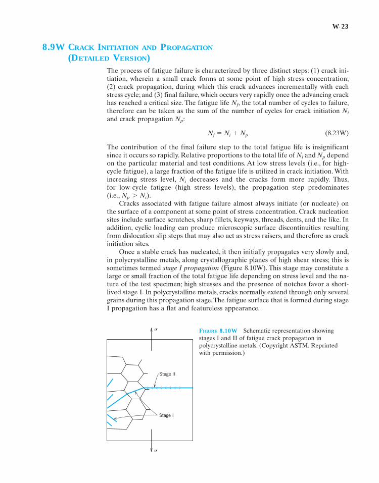
Stress intensity factor range, ∆K(103 psi in.)
MPa m
Cra
ck g
row
th r
ate,
(i
n./c
ycle
)
10 20 40 60 80 100
20 40 60 80 100
10–6
10–5
10–4
10–2
10–3
10–4
10–3
0.2% yield strength = 84,500 psiTest temp. = 24°C (75°F)Test frequency = 1800 cpm (30 Hz)Max. cyclic load, lbf
4000
5000
6000
7000
8000
9200
9900
da
dN
Cra
ck g
row
th r
ate,
(m
m/c
ycle
)d
ad
N
wc08.10.qxd 05/16/2002 11:51 AM Page 29
W-30
such plot for a Ni–Mo–V steel alloy. The linearity of the data may be noted, whichverifies the power law relationship of Equation 8.24W.
One of the goals of failure analysis is to be able to predict fatigue life for somecomponent, given its service constraints and laboratory test data. We are now ableto develop an analytical expression for Nf, due to stage II, by integration of Equation8.24W. Rearrangement is first necessary as follows:
(8.27W)
which may be integrated as
(8.28W)
The limits on the second integral are between the initial flaw length a0, which maybe measured using nondestructive examination techniques, and the critical cracklength ac determined from fracture toughness tests.
Substitution of the expression for �K (Equation 8.25bW) leads to
(8.29W)
Here it is assumed that �� (or �max � �min) is constant; furthermore, in general Ywill depend on crack length a and therefore cannot be removed from within theintegral.
A word of caution: Equation 8.29W presumes the validity of Equation 8.24Wover the entire life of the component; it ignores the time taken to initiate the crackand also for final failure. Therefore, this expression should only be taken as anestimate of Nf.
DESIGN EXAMPLE 8.2W
A relatively large sheet of steel is to be exposed to cyclic tensile and compressivestresses of magnitudes 100 MPa and 50 MPa, respectively. Prior to testing, it hasbeen determined that the length of the largest surface crack is 2.0 mm (2 � 10�3 m).Estimate the fatigue life of this sheet if its plane strain fracture toughness is25 and the values of m and A in Equation 8.24W are 3.0 and 1.0 � 10�12,respectively, for �� in MPa and a in m.Assume that the parameter Y is independentof crack length and has a value of 1.0.
SOLUTION
It first becomes necessary to compute the critical crack length ac, the integrationupper limit in Equation 8.29W. Equation 8.16W is employed for this computation,assuming a stress level of 100 MPa, since this is the maximum tensile stress.
MPa1m
�1
Ap m�21¢s2m �
ac
a0
daY
ma m�2
Nf � �ac
a0
da
A1Y¢s1pa2m
Nf � �Nf
0dN � �
ac
a0
daA1¢K2m
dN �da
A1¢K2m
wc08.10.qxd 05/16/2002 11:51 AM Page 30

W-31
Therefore,
We now want to solve Equation 8.29W using 0.002 m as the lower integration limita0, as stipulated in the problem. The value of �� is just 100 MPa, the magnitude ofthe tensile stress, since �min is compressive. Therefore, integration yields
� 5.49 � 106 cycles
�2
11.0 � 10�122 1p23�21100231123 a 110.002�
110.02b
�2
Ap3�21¢s23 Y 3 a 11a0
�11ac
b �
1Ap3�21¢s23 Y 3 1�22a�1�2 `
ac
a0
�1
Ap3�21¢s23 Y 3 �ac
a0
a�3�2 da
Nf �1
Ap m�21¢s2m �
ac
a0
daY
ma m�2
�1p
a 25 MPa1m1100 MPa2 112 b
2
� 0.02 m
ac �1p
aKIc
sYb2
wc08.10.qxd 05/16/2002 11:51 AM Page 31

W-32
C A S E S T U D Y8.13W AUTOMOBILE VALVE SPRING
MECHANICS OF SPRING DEFORMATIONThe basic function of a spring is to store mechanical energy as it is initially elasti-cally deformed and then recoup this energy at a later time as the spring recoils. Inthis section helical springs that are used in mattresses and in retractable pens andas suspension springs in automobiles are discussed. A stress analysis will be con-ducted on this type of spring, and the results will then be applied to a valve springthat is utilized in automobile engines.
Consider the helical spring shown in Figure 8.18W, which has been constructedof wire having a circular cross section of diameter d; the coil center-to-center di-ameter is denoted as D. The application of a compressive force F causes a twistingforce, or moment, denoted T, as shown in the figure.A combination of shear stressesresult, the sum of which, �, is
(8.30W)
where Kw is a force-independent constant that is a function of the D�d ratio:
(8.31W)
In response to the force F, the coiled spring will experience deflection, whichwill be assumed to be totally elastic. The amount of deflection per coil of spring, �c,as indicated in Figure 8.19W, is given by the expression
(8.32W)
where G is the shear modulus of the material from which the spring is constructed.Furthermore, �c may be computed from the total spring deflection, �s, and the
dc �8 FD3
d 4G
Kw � 1.60 aDdb�0.140
t �8FDpd3 Kw
FIGURE 8.18W Schematicdiagram of a helical springshowing the twisting momentT that results from thecompressive force F. (Adaptedfrom K. Edwards and P.McKee, Fundamentals ofMechanical Component Design.Copyright © 1991 by McGraw-Hill, Inc. Reproduced withpermission of The McGraw-HillCompanies.)
DF
F
T
d
wc08.13.qxd 05/16/2002 11:52 AM Page 32

W-33
number of effective spring coils, Nc, as
(8.33W)
Now, solving for F in Equation 8.32W gives
(8.34W)
and substituting for F in Equation 8.30W leads to
(8.35W)
Under normal circumstances, it is desired that a spring experience no per-manent deformation upon loading; this means that the right-hand side of Equa-tion 8.35W must be less than the shear yield strength �y of the spring material, orthat
(8.36W)
AUTOMOBILE VALVE SPRINGWe shall now apply the results of the preceding section to an automobile valvespring.A cutaway schematic diagram of an automobile engine showing these springsis presented in Figure 8.20W. Functionally, springs of this type permit both intakeand exhaust valves to alternately open and close as the engine is in operation. Ro-tation of the camshaft causes a valve to open and its spring to be compressed, sothat the load on the spring is increased. The stored energy in the spring then forcesthe valve to close as the camshaft continues its rotation.This process occurs for eachvalve for each engine cycle, and over the lifetime of the engine it occurs many mil-lions of times. Furthermore, during normal engine operation, the temperature ofthe springs is approximately 80�C (175�F).
ty 7dcGd
pD2 Kw
t �dcGd
pD2 Kw
F �d4dcG
8D3
dc �ds
Nc
FIGURE 8.19W Schematic diagrams of one coil of a helical spring, (a) prior tobeing compressed, and (b) showing the deflection �c produced from thecompressive force F. (Adapted from K. Edwards and P. McKee, Fundamentalsof Mechanical Component Design. Copyright © 1991 by McGraw-Hill, Inc.Reproduced with permission of The McGraw-Hill Companies.)
D2
D2
(a)
D2
F
(b)
c�
wc08.13.qxd 05/16/2002 11:52 AM Page 33

W-34
A photograph of a typical valve spring is shown in Figure 8.21W. The springhas a total length of 1.67 in. (42 mm), is constructed of wire having a diameter d of0.170 in. (4.3 mm), has six coils (only four of which are active), and has a center-to-center diameter D of 1.062 in. (27 mm). Furthermore, when installed and when avalve is completely closed, its spring is compressed a total of 0.24 in. (6.1 mm),
FIGURE 8.20W Cutaway drawing of asection of an automobile engine inwhich various components includingvalves and valve springs are shown.
FIGURE 8.21W Photograph of a typicalautomobile valve spring.
Cam
Camshaft
Exhaustvalve
Piston
Valvespring
Intakevalve
Crankshaft
wc08.13.qxd 05/16/2002 11:52 AM Page 34
W-35
which, from Equation 8.33W, gives an installed deflection per coil �ic of
The cam lift is 0.30 in. (7.6 mm), which means that when the cam completely opensa valve, the spring experiences a maximum total deflection equal to the sum ofthe valve lift and the compressed deflection, namely, 0.30 in. � 0.24 in. � 0.54 in.(13.7 mm). Hence, the maximum deflection per coil, �mc, is
Thus, we have available all of the parameters in Equation 8.36W (taking �c � �mc),except for �y, the required shear yield strength of the spring material.
However, the material parameter of interest is really not �y inasmuch asthe spring is continually stress cycled as the valve opens and closes during engineoperation; this necessitates designing against the possibility of failure by fatiguerather than against the possibility of yielding.This fatigue complication is handledby choosing a metal alloy that has a fatigue limit (Figure 8.17a) that is greaterthan the cyclic stress amplitude to which the spring will be subjected. For thisreason, steel alloys, which have fatigue limits, are normally employed for valvesprings.
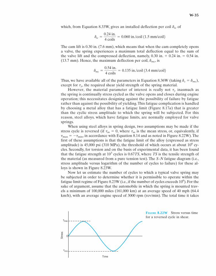
When using steel alloys in spring design, two assumptions may be made if thestress cycle is reversed (if �m � 0, where �m is the mean stress, or, equivalently, if�max � ��min, in accordance with Equation 8.14 and as noted in Figure 8.22W). Thefirst of these assumptions is that the fatigue limit of the alloy (expressed as stressamplitude) is 45,000 psi (310 MPa), the threshold of which occurs at about 106 cy-cles. Secondly, for torsion and on the basis of experimental data, it has been foundthat the fatigue strength at 103 cycles is 0.67TS, where TS is the tensile strength ofthe material (as measured from a pure tension test). The S–N fatigue diagram (i.e.,stress amplitude versus logarithm of the number of cycles to failure) for these al-loys is shown in Figure 8.23W.
Now let us estimate the number of cycles to which a typical valve spring maybe subjected in order to determine whether it is permissible to operate within thefatigue limit regime of Figure 8.23W (i.e., if the number of cycles exceeds 106). For thesake of argument, assume that the automobile in which the spring is mounted trav-els a minimum of 100,000 miles (161,000 km) at an average speed of 40 mph (64.4km/h), with an average engine speed of 3000 rpm (rev/min). The total time it takes
dmc �0.54 in.4 coils
� 0.135 in./coil 13.4 mm/coil2
dic �0.24 in.4 coils
� 0.060 in./coil 11.5 mm/coil2
FIGURE 8.22W Stress versus timefor a reversed cycle in shear.
Time
Str
ess
max
0
min�
�
wc08.13.qxd 05/16/2002 11:52 AM Page 35

the automobile to travel this distance is 2500 h (100,000 mi/40 mph), or 150,000 min.At 3000 rpm, the total number of revolutions is (3000 rev/min)(150,000 min) � 4.5� 108 rev, and since there are 2 rev/cycle, the total number of cycles is 2.25 � 108.This result means that we may use the fatigue limit as the design stress inasmuch asthe limit cycle threshold has been exceeded for the 100,000-mile distance of travel(i.e., since 2.25 � 108 cycles � 106 cycles).
Furthermore, this problem is complicated by the fact that the stress cycle isnot completely reversed (i.e., ) inasmuch as between minimum and maxi-mum deflections the spring remains in compression; thus, the 45,000 psi (310 MPa)fatigue limit is not valid. What we would now like to do is first to make an ap-propriate extrapolation of the fatigue limit for this case and then computeand compare with this limit the actual stress amplitude for the spring; if the stressamplitude is significantly below the extrapolated limit, then the spring design issatisfactory.
A reasonable extrapolation of the fatigue limit for this situation may bemade using the following expression (termed Goodman’s law):
(8.37W)
where �al is the fatigue limit for the mean stress �m; �e is the fatigue limit for �m � 0[i.e., 45,000 psi (310 MPa)]; and, again, TS is the tensile strength of the alloy. Todetermine the new fatigue limit �al from the above expression necessitates thecomputation of both the tensile strength of the alloy and the mean stress forthe spring.
One common spring alloy is an ASTM 232 chrome–vanadium steel, having acomposition of 0.48–0.53 wt% C, 0.80–1.10 wt% Cr, a minimum of 0.15 wt% V, andthe balance being Fe. Spring wire is normally cold drawn (Section 11.4) to the desireddiameter; consequently, tensile strength will increase with the amount of drawing(i.e., with decreasing diameter). For this alloy it has been experimentally verifiedthat, for the diameter d in inches, the tensile strength is
(8.38W)TS 1psi2 � 169,0001d2�0.167
tal � te a1 �
tm
0.67TSb
tm � 0
tm � 0
tm � 0
W-36
FIGURE 8.23W Shearstress amplitude versuslogarithm of the numberof cycles to fatigue failurefor typical ferrous alloys.
0.67TS
45,000 psi
Str
ess
ampl
itud
e, S
103 105 107 109
Cycles to failure, N(logarithmic scale)
wc08.13.qxd 05/16/2002 11:52 AM Page 36

W-37
Since d � 0.170 in. for this spring,
Computation of the mean stress �m is made using Equation 8.14 modified tothe shear stress situation as follows:
(8.39W)
It now becomes necessary to determine the minimum and maximum shear stressesfor the spring, using Equation 8.35W. The value of �min may be calculated fromEquations 8.35W and 8.31W inasmuch as the minimum �c is known (i.e., �ic � 0.060in.). A shear modulus of 11.5 � 106 psi (79 GPa) will be assumed for the steel; thisis the room-temperature value, which is also valid at the 80�C service temperature.Thus, �min is just
(8.40aW)
Now �max may be determined taking �c � �mc � 0.135 in. as follows:
(8.40bW)
Now, from Equation 8.39W,
The variation of shear stress with time for this valve spring is noted in Figure 8.24W;the time axis is not scaled, inasmuch as the time scale will depend on engine speed.
Our next objective is to determine the fatigue limit amplitude (�al) for this�m � 66,600 psi (460 MPa) using Equation 8.37W and for �e and TS values of45,000 psi (310 MPa) and 227,200 psi (1570 MPa), respectively. Thus,
� 25,300 psi 1175 MPa2 � 145,000 psi2 c1 �
66,600 psi
10.672 1227,200 psi2 d tal � te c1 �
tm
0.67TSd
�41,000 psi � 92,200 psi
2� 66,600 psi 1460 MPa2
tm �tmin � tmax
2
� 92,200 psi 1635 MPa2 � c 10.135 in.2 111.5 � 106 psi2 10.170 in.2
p11.062 in.22 d c1.60 a1.062 in.0.170 in.
b�0.140 d
tmax �dmcGd
pD2 c1.60 aDdb�0.140 d
� 41,000 psi 1280 MPa2 � c 10.060 in.2 111.5 � 106 psi2 10.170 in.2
p11.062 in.22 d c1.60 a1.062 in.0.170 in.
b�0.140 d �dicGd
pD2 c1.60 aDdb�0.140 d
tmin �dicGd
pD2 Kw
tm �tmin � tmax
2
� 227,200 psi 11570 MPa2 TS � 1169,0002 10.170 in.2�0.167
wc08.13.qxd 05/16/2002 11:52 AM Page 37

Now let us determine the actual stress amplitude �aa for the valve spring usingEquation 8.16 modified to the shear stress condition:
(8.41W)
Thus, the actual stress amplitude is slightly greater than the fatigue limit, whichmeans that this spring design is marginal.
The fatigue limit of this alloy may be increased to greater than 25,300 psi(175 MPa) by shot peening, a procedure described in Section 8.11. Shot peeninginvolves the introduction of residual compressive surface stresses by plasticallydeforming outer surface regions; small and very hard particles are projected ontothe surface at high velocities. This is an automated procedure commonly usedto improve the fatigue resistance of valve springs; in fact, the spring shown inFigure 8.21W has been shot peened, which accounts for its rough surface texture.Shot peening has been observed to increase the fatigue limit of steel alloys inexcess of 50% and, in addition, to reduce significantly the degree of scatter offatigue data.
This spring design, including shot peening, may be satisfactory; however, itsadequacy should be verified by experimental testing. The testing procedure isrelatively complicated and, consequently, will not be discussed in detail. Inessence, it involves performing a relatively large number of fatigue tests (on theorder of 1000) on this shot-peened ASTM 232 steel, in shear, using a mean stressof 66,600 psi (460 MPa) and a stress amplitude of 25,600 psi (177 MPa), and for106 cycles. On the basis of the number of failures, an estimate of the survivalprobability can be made. For the sake of argument, let us assume that this prob-ability turns out to be 0.99999; this means that one spring in 100,000 producedwill fail.
Suppose that you are employed by one of the large automobile companies thatmanufactures on the order of 1 million cars per year, and that the engine poweringeach automobile is a six-cylinder one. Since for each cylinder there are two valves,and thus two valve springs, a total of 12 million springs would be produced everyyear. For the above survival probability rate, the total number of spring failures
�92,200 psi � 41,000 psi
2� 25,600 psi 1177 MPa2
taa �tmax � tmin
2
W-38
FIGURE 8.24W Shear stressversus time for an automobilevalve spring.
100
80
60
40
20
0Time
Str
ess
(10
3 p
si)
�max = 92,200 psi
�aa = 25,600 psi
�min = 41,000 psi
�m = 66,600 psi
wc08.13.qxd 05/16/2002 11:52 AM Page 38

W-39
would be approximately 120, which also corresponds to 120 engine failures. As apractical matter, one would have to weigh the cost of replacing these 120 enginesagainst the cost of a spring redesign.
Redesign options would involve taking measures to reduce the shear stresseson the spring, by altering the parameters in Equations 8.31W and 8.35W.This wouldinclude either (1) increasing the coil diameter D, which would also necessitate in-creasing the wire diameter d, or (2) increasing the number of coils Nc.
wc08.13.qxd 05/16/2002 11:52 AM Page 39

8.16W DATA EXTRAPOLATION METHODS
The need often arises for engineering creep data that are impractical to collect fromnormal laboratory tests. This is especially true for prolonged exposures (on the or-der of years). One solution to this problem involves performing creep and/or creeprupture tests at temperatures in excess of those required, for shorter time periods,and at a comparable stress level, and then making a suitable extrapolation to thein-service condition. A commonly used extrapolation procedure employs theLarson–Miller parameter, defined as
(8.42W)
where C is a constant (usually on the order of 20), for T in Kelvin and the rupturelifetime tr in hours. The rupture lifetime of a given material measured at somespecific stress level will vary with temperature such that this parameter remainsconstant. Or, the data may be plotted as the logarithm of stress versus theLarson–Miller parameter, as shown in Figure 8.25W. Utilization of this techniqueis demonstrated in the following design example.
T1C � log tr2
DESIGN EXAMPLE 8.3W
Using the Larson–Miller data for S-590 iron shown in Figure 8.25W, predict the timeto rupture for a component that is subjected to a stress of 140 MPa (20,000 psi)at 800�C (1073 K).
Str
ess
(10
3 p
si)
Str
ess
(MP
a)
103 T (20 + log tr)(°R–h)
103 T(20 + log tr)(K–h)
25 30 35 40 45
12 16 20 24 28
50
100
10
1
1000
100
10
FIGURE 8.25W Logarithmstress versus theLarson–Miller parameter foran S-590 iron. (From F. R.Larson and J. Miller, Trans.ASME, 74, 765, 1952.Reprinted by permissionof ASME.)
W-40
wc08.16.qxd 05/16/2002 11:53 AM Page 40

W-41
SOLUTION
From Figure 8.25W, at 140 MPa (20,000 psi) the value of the Larson–Millerparameter is 24.0 � 103, for T in K and tr in h; therefore,
and, solving for the time,
tr � 233 h 19.7 days2
22.37 � 20 � log tr
� 1073120 � log tr2
24.0 � 103 � T120 � log tr2
wc08.16.qxd 05/16/2002 11:53 AM Page 41

9.16W THE GIBBS PHASE RULE
The construction of phase diagrams as well as some of the principles governing theconditions for phase equilibria are dictated by laws of thermodynamics. One of theseis the Gibbs phase rule, proposed by the nineteenth-century physicist J. WillardGibbs. This rule represents a criterion for the number of phases that will coexistwithin a system at equilibrium, and is expressed by the simple equation
(9.1W)
where P is the number of phases present (the phase concept is discussed in Section9.3). The parameter F is termed the number of degrees of freedom or the numberof externally controlled variables (e.g., temperature, pressure, composition) whichmust be specified to completely define the state of the system. Expressed anotherway, F is the number of these variables that can be changed independently withoutaltering the number of phases that coexist at equilibrium. The parameter C inEquation 9.1W represents the number of components in the system. Componentsare normally elements or stable compounds and, in the case of phase diagrams, arethe materials at the two extremities of the horizontal compositional axis (e.g., H2Oand C12H22O11, and Cu and Ni for the phase diagrams shown in Figures 9.1 and9.2a, respectively). Finally, N in Equation 9.1W is the number of noncompositionalvariables (e.g., temperature and pressure).
Let us demonstrate the phase rule by applying it to binary temperature–composition phase diagrams, specifically the copper–silver system, Figure 9.6. Sincepressure is constant (1 atm), the parameter N is 1—temperature is the only non-compositional variable. Equation 9.1W now takes the form
(9.2W)
Furthermore, the number of components C is 2 (viz Cu and Ag), and
or
Consider the case of single-phase fields on the phase diagram (e.g., �, �, andliquid regions). Since only one phase is present, P � 1 and
� 3 � 1 � 2
F � 3 � P
F � 3 � P
P � F � 2 � 1 � 3
P � F � C � 1
P � F � C � N
W-42
C h a p t e r 9 / Phase Diagrams
wc09.16.qxd 05/16/2002 13:15 PM Page 42

W-43
This means that to completely describe the characteristics of any alloy that existswithin one of these phase fields, we must specify two parameters; these are com-position and temperature, which locate, respectively, the horizontal and verticalpositions of the alloy on the phase diagram.
For the situation wherein two phases coexist, for example, � � L, � � L, and� � � phase regions, Figure 9.6, the phase rule stipulates that we have but onedegree of freedom since
Thus, it is necessary to specify either temperature or the composition of one of thephases to completely define the system. For example, suppose that we decide tospecify temperature for the � � L phase region, say, T1 in Figure 9.1W. Thecompositions of the � and liquid phases (C� and CL) are thus dictated by the ex-tremities of the tie line constructed at T1 across the � � L field. Note that only thenature of the phases is important in this treatment and not the relative phaseamounts. This is to say that the overall alloy composition could lie anywhere alongthis tie line constructed at temperature T1 and still give C� and CL compositionsfor the respective � and liquid phases.
The second alternative is to stipulate the composition of one of the phases forthis two-phase situation, which thereby fixes completely the state of the system. Forexample, if we specified C� as the composition of the � phase that is in equilibriumwith the liquid (Figure 9.1W), then both the temperature of the alloy (T1) and thecomposition of the liquid phase (CL) are established, again by the tie line drawnacross the � � L phase field so as to give this C� composition.
� 3 � 2 � 1
F � 3 � P
FIGURE 9.1W Enlargedcopper-rich section of theCu–Ag phase diagram inwhich the Gibbs phase rulefor the coexistence of twophases (i.e., � and L) isdemonstrated. Once thecomposition of either phase(i.e., C� or CL) or thetemperature (i.e., T1) isspecified, values for the tworemaining parameters areestablished by constructionof the appropriate tie line.
Composition (wt% Ag)(Cu)
Tem
pera
ture
(°C
)
0 20 40 60
600
800
L
C�
T1
CL� + L
1000
400
�
wc09.16.qxd 05/16/2002 13:15 PM Page 43

For binary systems, when three phases are present, there are no degrees offreedom, since
This means that the compositions of all three phases as well as the temperature arefixed. This condition is met for a eutectic system by the eutectic isotherm; for theCu–Ag system (Figure 9.6), it is the horizontal line that extends between points Band G. At this temperature, 779�C, the points at which each of the �, L, and � phasefields touch the isotherm line correspond to the respective phase compositions;namely, the composition of the � phase is fixed at 8.0 wt% Ag, that of the liquid at71.9 wt% Ag, and that of the � phase at 91.2 wt% Ag. Thus, three-phase equilib-rium will not be represented by a phase field, but rather by the unique horizontalisotherm line. Furthermore, all three phases will be in equilibrium for any alloycomposition that lies along the length of the eutectic isotherm (e.g., for the Cu–Agsystem at 779�C and compositions between 8.0 and 91.2 wt% Ag).
One use of the Gibbs phase rule is in analyzing for nonequilibrium conditions.For example, a microstructure for a binary alloy that developed over a range oftemperatures and consisting of three phases is a nonequilibrium one; under thesecircumstances, three phases will exist only at a single temperature.
� 3 � 3 � 0
F � 3 � P
W-44
wc09.16.qxd 05/16/2002 13:15 PM Page 44

W-45
C h a p t e r 10 / Phase Transformationsin Metals:
Development of Microstructure and Alteration of Mechanical Properties
10.3W THE KINETICS OF PHASE TRANSFORMATIONS
With phase transformations, normally at least one new phase is formed that hasdifferent physical/chemical characteristics and/or a different structure than theparent phase. Furthermore, most phase transformations do not occur instanta-neously. Rather, they begin by the formation of numerous small particles of thenew phase(s), which increase in size until the transformation has reached com-pletion. The progress of a phase transformation may be broken down into twodistinct stages: nucleation and growth. Nucleation involves the appearance of verysmall particles, or nuclei of the new phase (often consisting of only a few hundredatoms), which are capable of growing. During the growth stage these nuclei in-crease in size, which results in the disappearance of some (or all) of the parentphase. The transformation reaches completion if the growth of these new phaseparticles is allowed to proceed until the equilibrium fraction is attained. We nowdiscuss the mechanics of these two processes, and how they relate to solid-statetransformations.
NUCLEATIONThere are two types of nucleation: homogeneous and heterogeneous. The distinctionbetween them is made according to the site at which nucleating events occur. Forthe homogeneous type, nuclei of the new phase form uniformly throughout theparent phase, whereas for the heterogeneous type, nuclei form preferentially atstructural inhomogeneities, such as, container surfaces, insoluble impurities, grainboundaries, dislocations, and so on. We begin by discussing homogeneous nucle-ation because its description and theory are simpler to treat. These principles arethen extended to a discussion of the heterogeneous type.
Homogeneous NucleationA discussion of the theory of nucleation involves a thermodynamic parameter calledfree energy (or Gibbs free energy), G. In brief, free energy is a function of otherthermodynamic parameters, of which one is the internal energy of the system (i.e.,the enthalpy, H), and another is a measurement of the randomness or disorder ofthe atoms or molecules (i.e., the entropy, S). It is not our purpose here to providea detailed discussion of the principles of thermodynamics as they apply to materialssystems. However, relative to phase transformations, an important thermodynamicparameter is the change in free energy �G; a transformation will occur spontaneouslyonly when �G has a negative value.
For the sake of simplicity, let us first consider the solidification of a pure ma-terial, and that nuclei of the solid phase form in the interior of the liquid as atomscluster together so as to form a packing arrangement similar to that found in thesolid phase. Furthermore, it will be assumed that each nucleus is spherical in geom-etry and has a radius r. This situation is represented schematically in Figure 10.1W.
wc10.3.qxd 05/16/2002 13:20 PM Page 45

W-46
There are two contributions to the total free energy change that accompany asolidification transformation. The first is the free energy difference between thesolid and liquid phases, or the volume free energy, �Gv. Its value will be negative,and the magnitude of its contribution is the product of �Gv and the volume of thespherical nucleus (i.e., ). The second energy contribution results from the for-mation of the solid–liquid phase boundary during the solidification transformation.Associated with this boundary is a surface free energy, �, which is positive;furthermore, the magnitude of this contribution is the product of � and the surfacearea of the nucleus (i.e., 4�r2). Finally, the total free energy change is equal to thesum of these two contributions—that is,
(10.1W)
These volume, surface, and total free energy contributions are plotted schematicallyas a function of nucleus radius in Figures 10.2aW and 10.2bW. Here (Figure 10.2aW)it will be noted that for the curve corresponding to the first term on the right-handside of Equation 10.1W, the free energy (which is negative) decreases with the thirdpower of r. Furthermore, for the curve resulting from the second term in Equation10.1W, energy values are positive and increase with the square of the radius. Con-sequently, the curve associated with the sum of both terms (Figure 10.2bW) first in-creases, passes through a maximum, and finally decreases. In a physical sense, thismeans that as a solid particle begins to form as atoms in the liquid cluster together,
¢G � 43pr3¢Gv � 4pr2g
43 pr3
Volume =
Solid
Solid-liquidinterface
Area = 4�r2
r
Liquid�r34
3
FIGURE 10.1W Schematic diagram showing thenucleation of a spherical solid particle in a liquid.
FIGURE 10.2W (a) Schematic curves for volume free energy and surface freeenergy contributions to the total free energy change attending the formation of aspherical embryo/nucleus during solidification. (b) Schematic plot of free energyversus embryo/nucleus radius, on which is shown the critical free energy change(�G*) and the critical nucleus radius (r*).
0
–
+
radius, r
4�r2�
�r3∆Gv43
Free
ene
rgy
chan
ge,
∆G
(a) (b)
0
–
+
radius, r
r*
∆G*
Free
ene
rgy
chan
ge,
∆G
wc10.3.qxd 05/16/2002 13:20 PM Page 46

W-47
its free energy first increases. If this cluster reaches a size corresponding to the crit-ical radius r*, then growth will continue with the accompaniment of a decrease infree energy. On the other hand, a cluster of radius less than the critical will shrinkand redissolve. This subcritical particle is an embryo, whereas the particle of radiusgreater than r* is termed a nucleus. A critical free energy, �G*, occurs at the criti-cal radius and, consequently, at the maximum of the curve in Figure 10.2bW. This�G* corresponds to an activation free energy, which is the free energy required forthe formation of a stable nucleus. Equivalently, it may be considered an energy bar-rier to the nucleation process.
Since r* and �G* appear at the maximum on the free energy-versus-radiuscurve of Figure 10.2bW, derivation of expressions for these two parameters is a sim-ple matter. For r*, we differentiate the �G equation (Equation 10.1W) with respectto r, set the resulting expression equal to zero, and then solve for r (� r*). That is,
(10.2W)
which leads to the result
(10.3W)
Now, substitution of this expression for r* into Equation 10.1W yields the followingexpression for �G*:
(10.4W)
This volume free energy change �Gv is the driving force for the solidificationtransformation, and its magnitude is a function of temperature. At the equilibriumsolidification temperature Tm, the value of �Gv is zero, and with diminishingtemperature its value becomes increasingly more negative.
It can be shown that �Gv is a function of temperature as
(10.5W)
where �Hf is the latent heat of fusion (i.e., the heat given up during solidification),and Tm and the temperature T are in Kelvin. Substitution of this expression for �Gv
into Equations 10.3W and 10.4W yields
(10.6W)
and
(10.7W)¢G* � a16pg3T 2m
3¢H 2f
b
11Tm � T22
r* � a�2gTm
¢Hfb a 1
Tm � Tb
¢Gv �¢Hf 1Tm � T 2Tm
¢G* �16pg3
31¢Gv22
r* � �2g
¢Gv
d1¢G2dr
� 43 p¢Gv13r22 � 4pg12r2 � 0
wc10.3.qxd 05/16/2002 13:20 PM Page 47

W-48
Thus, from these two equations, both the critical radius r* and the activation freeenergy �G* decrease as temperature T decreases. (The � and �Hf parameters inthese expressions are relatively insensitive to temperature changes.) Figure 10.3W,a schematic �G-versus-r plot that shows curves for two different temperatures,illustrates these relationships. Physically, this means that with a lowering of tem-perature at temperatures below the equilibrium solidification temperature (Tm),nucleation occurs more readily. Furthermore, the number of stable nuclei n* (hav-ing radii greater than r*) is a function of temperature as
(10.8W)
where the constant K1 is related to the total number of nuclei of the solid phase.For the exponential term of this expression, changes in temperature have a greateraffect on the magnitude of the �G* term in the numerator than the T term in thedenominator. Consequently, as the temperature is lowered below Tm the exponen-tial term in Equation 10.8W also decreases such that the magnitude of n* increases.This temperature dependence (n* versus T) is represented in the schematic plot ofFigure 10.4aW.
There is another important temperature-dependent step that is involved in andalso influences nucleation: the clustering of atoms by short-range diffusion duringthe formation of nuclei. The influence of temperature on the rate of diffusion (i.e.,
n* � K1 exp a�¢G*
kTb
0
–
+
1
1
radius, r
T2 > T1
at T1
at T2
r*
∆G*
∆G*∆G
2r*
2
FIGURE 10.3W Schematic free-energy-versus-embryo/nucleus-radius curves for two differenttemperatures. The critical freeenergy change (�G*) and criticalnucleus radius (r*) are indicatedfor each temperature.
FIGURE 10.4W For solidification, schematic plots of (a) number of stable nucleiversus temperature, (b) frequency of atomic attachment versus temperature, and(c) nucleation rate versus temperature (also shown are curves for parts a and b).
Number of stable nuclei, n*
exp – ∆G*kTTe
mpe
ratu
re
Tm
Frequency of attachment, �d
exp –QdkT
Tem
pera
ture
Tm
n*, �d, N
�d
.
.
n*
N
∆T
Tem
pera
ture
Tm
(a) (b) (c)
wc10.3.qxd 05/16/2002 13:20 PM Page 48

W-49
magnitude of the diffusion coefficient, D) is given in Equation 5.8. Furthermore,this diffusion effect is related to the frequency at which atoms from the liquid at-tach themselves to the solid nucleus, �d. Or, the dependence of �d on temperatureis the same as for the diffusion coefficient—namely,
(10.9W)
where Qd is a temperature-independent parameter—the activation energy fordiffusion—and K2 is a temperature-independent constant. Thus, from Equation10.9W a diminishment of temperature results in a reduction in �d. This effect, rep-resented by the curve shown in Figure 10.4bW, is just the reverse of that for n* asdiscussed above.
The principles and concepts just developed are now extended to a discussionof another important nucleation parameter, the nucleation rate (which has unitsof nuclei per unit volume per second). This rate is simply proportional to the prod-uct of n* (Equation 10.8W) and �d (Equation 10.9W); that is,
(10.10W)
Here K3 is the number of atoms on a nucleus surface. Figure 10.4cW schematicallyplots nucleation rate as a function of temperature and, in addition, the curves ofFigures 10.4aW and 10.4bW from which the curve is derived. Note (Figure10.4cW) that, with a lowering of temperature from below Tm, the nucleation ratefirst increases, achieves a maximum, and subsequently diminishes.
The shape of this curve is explained as follows: for the upper region ofthe curve (a sudden and dramatic increase in with decreasing T), �G* is greaterthan Qd, which means that the exp(��G*�kT) term of Equation 10.10W is muchsmaller than exp(�Qd�kT). In other words, the nucleation rate is suppressed at hightemperatures due to a small activation driving force. With continued diminishmentof temperature, there comes a point at which �G* becomes smaller than the tem-perature-independent Qd with the result that exp (�Qd�kT) � exp (��G*�kT),or that, at lower temperatures, a low atomic mobility suppresses the nucleationrate. This accounts for the shape of the lower curve segment (a precipitous reduc-tion of with a continued diminishment of temperature). Furthermore, the curveof Figure 10.4cW necessarily passes through a maximum over the intermediatetemperature range where values for �G* and Qd are of approximately the samemagnitude.
Several qualifying comments are in order regarding the above discussion. First,although we assumed a spherical shape for nuclei, this method may be applied toany shape with the same final result. Furthermore, this treatment may be utilizedfor types of transformations other than solidification (i.e., liquid–solid)—for exam-ple, solid–vapor and solid–solid. However, magnitudes of �Gv and �, in addition todiffusion rates of the atomic species, will undoubtedly differ among the varioustransformation types. In addition, for solid–solid transformations, there may be vol-ume changes attendant to the formation of new phases. These changes may lead tothe introduction of microscopic strains, which must be taken into account in the �Gexpression of Equation 10.1W, and, consequently, will affect the magnitudes of r*and �G*.
From Figure 10.4cW it is apparent that during the cooling of a liquid, an ap-preciable nucleation rate (i.e., solidification) will begin only after the temperature
N#
N#
N#N
#
N#
N#
� K3n*nd � K1K2K3 cexp a�¢G*kTb exp a�Qd
kTb d
N#
nd � K2 exp a�Qd
kTb
wc10.3.qxd 05/16/2002 13:20 PM Page 49

W-50
has been lowered to below the equilibrium solidification (or melting) temperature(Tm). This phenomenon is termed supercooling (or undercooling), and the degreeof supercooling for homogeneous nucleation may be significant (on the order ofseveral hundred degrees Kelvin) for some systems. In Table 10.1W is tabulated, forseveral materials, typical degrees of supercooling for homogeneous nucleation.
Heterogeneous NucleationAlthough levels of supercooling for homogeneous nucleation may be significant (onoccasion several hundred degrees Celsius), in practical situations they are often on theorder of only several degrees Celsius. The reason for this is that the activation energy(i.e., energy barrier) for nucleation (�G* of Equation 10.4W) is lowered when nucleiform on preexisting surfaces or interfaces, since the surface free energy (� of Equation10.4W) is reduced. In other words, it is easier for nucleation to occur at surfaces andinterfaces than at other sites. Again, this type of nucleation is termed heterogeneous.
In order to understand this phenomenon, let us consider the nucleation, on aflat surface, of a solid particle from a liquid phase. It is assumed that both the liquidand solid phases “wet” this flat surface, that is, both of these phases spread out andcover the surface; this configuration is depicted schematically in Figure 10.5W. Alsonoted in the figure are three interfacial energies (represented as vectors) that ex-ist at two-phase boundaries—�SL, �SI, and �IL—as well as the wetting angle � (theangle between the �SI and �SL vectors). Taking a surface tension force balance inthe plane of the flat surface leads to the following expression:
(10.11W)gIL � gSI � gSL cos u
Table 10.1W Degree of Supercooling(�T) Values (Homogeneous Nucleation)for Several Metals
Metal �T (�C )Antimony 135Germanium 227Silver 227Gold 230Copper 236Iron 295Nickel 319Cobalt 330Palladium 332
[From D. Turnbull and R. E. Cech, “MicroscopicObservation of the Solidification of Small MetalDroplets,” J. Appl. Phys., 21, 808 (1950)].
Surface or interface
Solid
Liquid
�
�SL
� IL
�SI
FIGURE 10.5W Heterogeneousnucleation of a solid from a liquid.The solid–surface (�SI), solid–liquid(�SL), and liquid–surface (�IL)interfacial energies are representedby vectors. The wetting angle (�) isalso shown.
wc10.3.qxd 05/16/2002 13:20 PM Page 50

W-51
1 For example, for � angles of 30� and 90�, values of S(�) are approximately 0.01 and 0.5,respectively.
Now, using a somewhat involved procedure similar to the one presented abovefor homogeneous nucleation (which we have chosen to omit), it is possible to deriveequations for r* and �G*; these are as follows:
(10.12W)
(10.13W)
The S(�) term of this last equation is a function only of � (i.e, the shape of thenucleus), which will have a numerical value between zero and unity.1
From Equation 10.12W, it is important to note that the critical radius r* forheterogeneous nucleation is the same as for homogeneous, inasmuch as �SL is thesame surface energy as � in Equation 10.3W. It is also evident that the activationenergy barrier for heterogeneous nucleation (Equation 10.13W) is smaller than thehomogeneous barrier (Equation 10.4W) by an amount corresponding to the valueof this S(�) function, or
(10.14W)
Figure 10.6W, a schematic graph of �G versus nucleus radius, plots curves forboth types of nucleation, and indicates the difference in the magnitudes of and , in addition to the constancy of r*. This lower �G* for heterogeneousmeans that a smaller energy must be overcome during the nucleation process(than for homogeneous), and, therefore, heterogeneous nucleation occurs morereadily (Equation 10.10W). In terms of the nucleation rate, the versus T curve(Figure 10.4cW) is shifted to higher temperatures for heterogeneous. This effectis represented in Figure 10.7W, which also shows that a much smaller degree ofsupercooling (�T) is required for heterogeneous nucleation.
N#
¢G*hom
¢G*het
¢G*het � ¢G*homS1u2
¢G* � a16pg3SL
3¢G2v
bS1u2
r* � �2gSL
¢Gv
0
∆G*∆G het
∆G*hom
r
r*
FIGURE 10.6W Schematic free-energy-versus-embryo/nucleus-radius plot on which is presentedcurves for both homogeneousand heterogeneous nucleation.Critical free energies and thecritical radius are also shown.
wc10.3.qxd 05/16/2002 13:20 PM Page 51

W-52
GROWTHThe growth step in a phase transformation begins once an embryo has exceededthe critical size, r*, and becomes a stable nucleus. Note that nucleation will continueto occur simultaneously with growth of the new phase particles; of course, nucle-ation cannot occur in regions that have already transformed to the new phase.Furthermore, the growth process will cease in any region where particles of the newphase meet, since here the transformation will have reached completion.
Particle growth occurs by long-range atomic diffusion, which normally involvesseveral steps—for example, diffusion through the parent phase, across a phaseboundary, and then into the nucleus. Consequently, the growth rate is determinedby the rate of diffusion, and its temperature dependence is the same as for the dif-fusion coefficient (Equation 5.8)—namely,
(10.15W)
where Q (the activation energy) and C (a preexponential) are independent of tem-perature.2 The temperature dependence of is represented by one of the curvesin Figure 10.8W; also shown is a curve for the nucleation rate, (again, almost al-ways the rate for heterogeneous nucleation). Now, at some temperature, the over-all transformation rate is equal to some product of and . The third curve ofFigure 10.8W, which is for the total rate, represents this combined effect. The gen-eral shape of this curve is the same as for the nucleation rate, in that it has a peakor maximum that has been shifted upward relative to the curve.
Whereas this treatment on transformation has been developed for solidifi-cation, the same general principles also apply to solid–solid and solid–gas trans-formations.
N#
G#
N#
N#G
#
G#
� C exp a� QkTb
G#
2 Processes the rates of which depend on temperature as in Equation 10.15W aresometimes termed thermally activated.
G#
Nucleation rate
∆Thom
het
∆Thet
N.
homN.
Tem
pera
ture
Tm
FIGURE 10.7W Nucleation rate versus temperature forboth homogeneous and heterogeneous nucleation.Degree of supercooling (�T) for each is also shown.
wc10.3.qxd 05/16/2002 13:20 PM Page 52

W-53
As we shall see below, the rate of transformation and the time required for thetransformation to proceed to some degree of completion (e.g., time to 50% reac-tion completion, t0.5) are inversely proportional to one another (Equation 10.17W).Thus, if the logarithm of this transformation time (i.e., log t0.5) is plotted versustemperature, a curve having the general shape shown in Figure 10.9bW results. This“C-shaped” curve is a virtual mirror image (through a vertical plane) of the trans-formation rate curve of Figure 10.8W, as demonstrated in Figure 10.9W. It is oftenthe case that the kinetics of phase transformations are represented using logarithmtime- (to some degree of transformation) versus-temperature plots (for example,see Section 10.5).
Several physical phenomena may be explained in terms of the transformationrate-versus-temperature curve of Figure 10.8W. First, the size of the product phaseparticles will depend on transformation temperature. For example, for transfor-mations that occur at temperatures near to Tm, corresponding to low nucleationand high growth rates, few nuclei form that grow rapidly. Thus, the resulting mi-crostructure will consist of few and relatively large phase particles (e.g., coarsegrains). Conversely, for transformations at lower temperatures, nucleation ratesare high and growth rates low, which results in many small particles (e.g., finegrains).
Also, from Figure 10.8W, when a material is cooled very rapidly through thetemperature range encompassed by the transformation rate curve to a relativelylow temperature where the rate is extremely low, it is possible to produce non-equilibrium phase structures [for example, see Sections 10.5 (or 10.5W) and 11.9]
Rate
Overalltransformation
rate
Nucleation rate, N.
Growth rate, G.
Tem
pera
ture
Tm
FIGURE 10.8W Schematic plot showingcurves for nucleation rate ( ), growth rate( ), and overall transformation rateversus temperature.G# N
#
Rate t0.5
1 Time (t0.5)(logarithmic scale)
Tem
pera
ture
Te
(a) (b)
Tem
pera
ture
Te
FIGURE 10.9W Schematic plots of (a)transformation rate versus temperature,and (b) logarithm time [to some degree
(e.g., 0.5 fraction) of transformation] versustemperature. The curves in both (a) and (b)
are generated from the same set of data—i.e., for horizontal axes, the time [scaled
logarithmically in the (b) plot] is just thereciprocal of the rate from plot (a).
wc10.3.qxd 05/16/2002 13:20 PM Page 53

W-54
Frac
tion
of
tran
sfor
mat
ion,
y
Nucleation Growth
t0.5
Logarithm of heating time, t
0
0.5
1.0 FIGURE 10.10W Plot of fractionreacted versus the logarithm oftime typical of many solid-statetransformations in whichtemperature is held constant.
KINETIC CONSIDERATIONS OF SOLID-STATETRANSFORMATIONSThe previous discussion of this section has centered on the temperature depen-dences of nucleation, growth, and transformation rates.The time dependence of rate(which is often termed the kinetics of a transformation) is also an importantconsideration, often in the heat treatment of materials. Also, since many transfor-mations of interest to materials scientists and engineers involve only solid phases,we have decided to devote the following discussion to the kinetics of solid-statetransformations.
With many kinetic investigations, the fraction of reaction that has occurred ismeasured as a function of time while the temperature is maintained constant.Trans-formation progress is usually ascertained by either microscopic examination ormeasurement of some physical property (such as electrical conductivity) the mag-nitude of which is distinctive of the new phase. Data are plotted as the fraction oftransformed material versus the logarithm of time; an S-shaped curve similar to thatin Figure 10.10W represents the typical kinetic behavior for most solid-state reac-tions. Nucleation and growth stages are also indicated in the figure.
For solid-state transformations displaying the kinetic behavior in Figure 10.10W,the fraction of transformation y is a function of time t as follows:
(10.16W)
where k and n are time-independent constants for the particular reaction.The aboveexpression is often referred to as the Avrami equation.
By convention, the rate of a transformation is taken as the reciprocal of timerequired for the transformation to proceed halfway to completion, t0.5, or
(10.17W)
Temperature will have a profound influence on the kinetics and thus on therate of a transformation. This is demonstrated in Figure 10.11W, where y-versus-log t
rate �1
t0.5
y � 1 � exp1�ktn2
wc10.3.qxd 05/16/2002 13:20 PM Page 54

W-55
S-shaped curves at several temperatures for the recrystallization of copper areshown.
A detailed discussion on the influence of both temperature and time on phasetransformations is provided in Section 10.5.
Time (min)(Logarithmic scale)
Per
cent
rec
ryst
alliz
ed1 10 102 1040
20
40
60 135°C 119°C 113°C 102°C 88°C 43°C
80
100
FIGURE 10.11W Percent recrystallization as a function of time and atconstant temperature for pure copper. (Reprinted with permission fromMetallurgical Transactions, Vol. 188, 1950, a publication of The MetallurgicalSociety of AIME, Warrendale, PA. Adapted from B. F. Decker and D. Harker,“Recrystallization in Rolled Copper,” Trans. AIME, 188, 1950, p. 888.)
wc10.3.qxd 05/16/2002 13:20 PM Page 55

W-56
10.5W ISOTHERMAL TRANSFORMATION DIAGRAMS
PEARLITE (PRINT)
BAINITE (DETAILED VERSION)From the discussion of the preceding section, it would seem reasonable to expectthe alternating ferrite and cementite lamellae to become thinner and thinner as theisothermal transformation temperature is lowered to below that at which finepearlite forms. Such is not the case; other microconstituents that are products ofthe austenitic transformation are found to exist at these lower temperatures. Oneof these microconstituents is called bainite. Furthermore, depending on transfor-mation temperature, two general types of bainite have been observed: upper andlower bainite. Like pearlite, the microstructure of each of these bainites consists offerrite and cementite phases; however, their arrangements are different from thealternating lamellar structure found in pearlite.
For temperatures between approximately 300 and 540�C, bainite forms as a se-ries of parallel laths (i.e., thin narrow strips) or needles of ferrite that are separatedby elongated particles of the cementite phase. Such is termed upper bainite, and itsmicrostructural details are so fine that their resolution is possible only using elec-tron microscopy. Figure 10.12aW is an electron micrograph that shows a grain ofupper bainite (positioned diagonally from lower left to upper right); the variousphases in this micrograph have been labeled. In addition, the phase that surroundsthe bainite is martensite, which is a topic addressed in a subsequent section.Furthermore, no proeutectoid phase forms with bainite.
At lower temperatures between about 200 and 300�C lower bainite is the trans-formation product. For lower bainite, the ferrite phase exists as thin plates (insteadof laths as with upper bainite), and narrow cementite particles (as very fine rods orblades) form within these ferrite plates. Figure 10.12bW is an electron micrographof lower bainite; in this micrograph, the plates of bainite appear as needle-like struc-tures, whereas the phase that surrounds them is martensite. Furthermore, the ce-mentite particles within these bainite plates are so small as not to be resolvable; theschematic inset shown with this micrograph represents the detailed structure ofthese plates.
The time–temperature dependence of the bainite transformation may alsobe represented on the isothermal transformation diagram. The transformationoccurs at temperatures below those at which pearlite forms; begin-, end-, andhalf-reaction curves are just extensions of those for the pearlitic transforma-tion, as shown in Figure 10.13W, the isothermal transformation diagram for aniron–carbon alloy of eutectoid composition that has been extended to lowertemperatures. All three curves are C-shaped and have a “nose” at point N, wherethe rate of transformation is a maximum. As may be noted, whereas pearliteforms above the nose—that is, over the temperature range of about 540 to 727�C(1000 to 1341�F)—for isothermal treatments at temperatures between about215 and 540�C (420 and 1000�F), bainite is the transformation product. Temper-ature regimes over which upper and lower bainites form are indicated onFigure 10.13W.
Note also that pearlitic and bainitic transformations are really competitive witheach other, and once some portion of an alloy has transformed to either pearliteor bainite, transformation to the other microconstituent is not possible withoutreheating to form austenite.
wc10.5.qxd 05/16/2002 13:22 PM Page 56

W-57
SPHEROIDITE (PRINT)
MARTENSITE (DETAILED VERSION)Yet another microconstituent or phase called martensite is formed when austeni-tized iron–carbon alloys are rapidly cooled (or quenched) to a relatively lowtemperature (in the vicinity of the ambient). Martensite is a nonequilibrium single-phase structure that results from a diffusionless transformation of austenite. It maybe thought of as a transformation product that is competitive with pearlite and bai-nite.The martensitic transformation occurs when the quenching rate is rapid enough
FIGURE 10.12W (a) Transmission electronmicrograph showing the structure of upper
bainite. A grain of bainite passes from lowerleft to upper right-hand corners, which con-sists of elongated and needle-shaped parti-
cles of Fe3C within a ferrite matrix. Thephase surrounding the bainite is martensite.
15,000�. (Reproduced with permission fromMetals Handbook, Vol. 8, 8th edition, Metall-
ography, Structures and Phase Diagrams,American Society for Metals, MaterialsPark, OH, 1973.) (b) Scanning electronmicrograph showing lower bainite in a
martensite matrix for an AISI steel that wastransformed isothermally at 300�C. The inset
shows the detail of a lower bainite grain.2300�. (From John D. Verhoeven,
Fundamentals of Physical Metallurgy, p. 502.Copyright © 1975 by John Wiley & Sons,
New York. Reprinted by permission of JohnWiley & Sons, Inc.)
(a)
Martensite
Cementite
Ferrite
Martensite
Cementite
Ferrite
(b)
wc10.5.qxd 05/16/2002 13:22 PM Page 57

W-58
to prevent carbon diffusion. Any diffusion whatsoever will result in the formationof ferrite and cementite phases.
The martensitic transformation is not well understood. However, large num-bers of atoms experience cooperative movements, in that there is only a slight dis-placement of each atom relative to its neighbors. This occurs in such a way thatthe FCC austenite experiences a polymorphic transformation to a body-centeredtetragonal (BCT) martensite. A unit cell of this crystal structure (Figure 10.14W)is simply a body-centered cube that has been elongated along one of its dimen-sions; this structure is distinctly different from that for BCC ferrite. All the car-bon atoms remain as interstitial impurities in martensite; as such, they constitutea supersaturated solid solution that is capable of rapidly transforming to otherstructures if heated to temperatures at which diffusion rates become appreciable.Many steels, however, retain their martensitic structure almost indefinitely at roomtemperature.
FIGURE 10.13WIsothermal
transformation diagramfor an iron–carbon
alloy of eutectoidcomposition, including
austenite-to-pearlite(A–P) and austenite-to-
bainite (A–B)transformations.[Adapted from
H. Boyer (Editor),Atlas of Isothermal
Transformation andCooling Transformation
Diagrams, AmericanSociety for Metals,
1977, p. 28.]
FIGURE 10.14W The body-centered tetragonal unit cell formartensitic steel showing iron atoms (circles) and sites thatmay be occupied by carbon atoms (crosses). For thistetragonal unit cell, c � a.
Time (s)
Tem
pera
ture
(°C
)
Tem
pera
ture
(°F
)
10–1 1 10 102 103 104 105
400
600
800
1000
1200
1400Eutectoid temperatureA
A
A
50%
N
B
Upperbainite
Lowerbainite
P
100
200
300
400
500
600
700
800
A+
P
A + B
c
aa
wc10.5.qxd 05/16/2002 13:22 PM Page 58

W-59
The martensitic transformation is not, however, unique to iron–carbon alloys.It is found in other systems and is characterized, in part, by the diffusionless trans-formation.
Since the martensitic transformation does not involve diffusion, it occurs al-most instantaneously; the martensite grains nucleate and grow at a very rapid rate—the velocity of sound within the austenite matrix. Thus the martensitic transforma-tion rate, for all practical purposes, is time independent.
Two distinctly different martensitic microstructures are found in iron–carbonalloys: lath and lenticular. For alloys containing less than about 0.6 wt% C, themartensite grains form as laths (i.e., long and thin plates, like blades of grass) thatform side by side and are aligned parallel to one another. Furthermore, these lathsare grouped into larger structural entities, called blocks; the morphology of this lath(or massive) martensite is represented schematically in Figure 10.15W. Microstruc-tural details of this type of martensite are too fine to be revealed by optical mi-croscopy, and, therefore, electron micrographic techniques must be employed.
Lenticular (or plate) martensite is typically found in iron–carbon alloyscontaining greater than approximately 0.6 wt% C. With this structure the marten-site grains take on a needle-like (i.e., lenticular) or plate-like appearance, asindicated in the photomicrograph of Figure 10.16W. Here the lenticular martensite
FIGURE 10.16W Photomicrograph showingthe lenticular or plate martensiticmicrostructure. The needle-shaped grains arethe martensite phase, and the white regionsare austenite that failed to transform duringthe rapid quench. 1220�. (Photomicrographcourtesy of United States SteelCorporation.)
FIGURE 10.15W Schematic diagramshowing the microstructural features of lathor massive martensite. [Adapted from A. R.Marder and J. I. Goldstein (Editors), PhaseTransformations in Ferrous Alloys, TheMetallurgical Society of AIME, 1984.]
Blocks
Laths
wc10.5.qxd 05/16/2002 13:22 PM Page 59
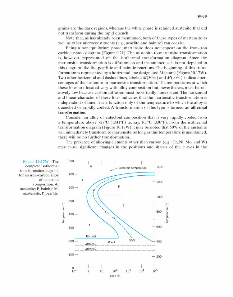
W-60
grains are the dark regions, whereas the white phase is retained austenite that didnot transform during the rapid quench.
Note that, as has already been mentioned, both of these types of martensite aswell as other microconstituents (e.g., pearlite and bainite) can coexist.
Being a nonequilibrium phase, martensite does not appear on the iron–ironcarbide phase diagram (Figure 9.21). The austenite-to-martensite transformationis, however, represented on the isothermal transformation diagram. Since themartensitic transformation is diffusionless and instantaneous, it is not depicted inthis diagram like the pearlitic and bainitic reactions. The beginning of this trans-formation is represented by a horizontal line designated M (start) (Figure 10.17W).Two other horizontal and dashed lines, labeled M(50%) and M(90%), indicate per-centages of the austenite-to-martensite transformation. The temperatures at whichthese lines are located vary with alloy composition but, nevertheless, must be rel-atively low because carbon diffusion must be virtually nonexistent. The horizontaland linear character of these lines indicates that the martensitic transformation isindependent of time; it is a function only of the temperature to which the alloy isquenched or rapidly cooled. A transformation of this type is termed an athermaltransformation.
Consider an alloy of eutectoid composition that is very rapidly cooled froma temperature above 727�C (1341�F) to, say, 165�C (330�F). From the isothermaltransformation diagram (Figure 10.17W) it may be noted that 50% of the austenitewill immediately transform to martensite; as long as this temperature is maintained,there will be no further transformation.
The presence of alloying elements other than carbon (e.g., Cr, Ni, Mo, and W)may cause significant changes in the positions and shapes of the curves in the
FIGURE 10.17W Thecomplete isothermal
transformation diagramfor an iron–carbon alloy
of eutectoidcomposition: A,
austenite; B, bainite; M,martensite; P, pearlite.
Time (s)
Tem
pera
ture
(°C
)
Tem
pera
ture
(°F
)
10–1 1 10 102 103 104 105
200
400
800
600
1000
1200
1400Eutectoid temperatureA
A
A
M + A
M(start)
M(50%)
M(90%)
50%
P
B
100
0
200
300
400
500
600
700
800
A
A
+
+
P
B
wc10.5.qxd 05/16/2002 13:22 PM Page 60

W-61
isothermal transformation diagrams. These changes include (1) shifting to longertimes the nose of the austenite-to-pearlite transformation (and also a proeutectoidphase nose, if such exists), and (2) the formation of a separate bainite nose. Thesealterations may be observed by comparing Figures 10.17W and 10.18W, which areisothermal transformation diagrams for carbon and alloy steels, respectively.
FIGURE 10.18WIsothermal
transformation diagramfor an alloy steel (type
4340): A, austenite;B, bainite; P, pearlite;
M, martensite;F, proeutectoid ferrite.
[Adapted fromH. Boyer (Editor),Atlas of Isothermal
Transformation andCooling Transformation
Diagrams, AmericanSociety for Metals, 1977,
p. 181.]
Time (s)
Tem
pera
ture
(°C
)
Tem
pera
ture
(°F
)
1 10 102 103 104 105 106
200
0
400
800
600
1000
1200
1400
Eutectoid temperature
A
A
A + F F + P
A + B
M + A
M(start)
M(50%)
M(90%)
50% B
M100
0
200
300
400
500
600
700
800
A + F + P
wc10.5.qxd 05/16/2002 13:22 PM Page 61

W-62
17.4W PREDICTION OF CORROSION RATES
POLARIZATIONConsider the standard Zn/H2 electrochemical cell shown in Figure 17.1W, which hasbeen short-circuited such that oxidation of zinc and reduction of hydrogen will occurat their respective electrode surfaces. The potentials of the two electrodes will notbe at the values determined from Table 17.1 because the system is now a nonequi-librium one.The displacement of each electrode potential from its equilibrium valueis termed polarization, and the magnitude of this displacement is the overvoltage,normally represented by the symbol �. Overvoltage is expressed in terms of plusor minus volts (or millivolts) relative to the equilibrium potential. For example, sup-pose that the zinc electrode in Figure 17.1W has a potential of �0.621 V after it hasbeen connected to the platinum electrode. The equilibrium potential is �0.763 V(Table 17.1), and, therefore,
There are two types of polarization—activation and concentration. We will nowdiscuss their mechanisms since they control the rate of electrochemical reactions.
Activation PolarizationAll electrochemical reactions consist of a sequence of steps that occur in series atthe interface between the metal electrode and the electrolyte solution. Activationpolarization refers to the condition wherein the reaction rate is controlled by the
h � �0.621 V � 1�0.763 V2 � �0.142 V
FIGURE 17.1W Electrochemicalcell consisting of standard zincand hydrogen electrodes that hasbeen short-circuited.
H2 Gas,1 atm
pressure
H2
e–
Zn
Zn2+ solution,1.0 M
Membrane
H+ solution,1.0 M
Zn2+ Pt 2H+
C h a p t e r 17 / Corrosion andDegradation of Materials
W-62
wc17.4 .qxd 05/16/2002 13:24 PM Page 62

W-63
one step in the series that occurs at the slowest rate. The term “activation” is ap-plied to this type of polarization because an activation energy barrier is associatedwith this slowest, rate-limiting step.
To illustrate, let us consider the reduction of hydrogen ions to form bubbles ofhydrogen gas on the surface of a zinc electrode (Figure 17.2W). It is conceivablethat this reaction could proceed by the following step sequence:
1. Adsorption of H� ions from the solution onto the zinc surface
2. Electron transfer from the zinc to form a hydrogen atom,
3. Combining of two hydrogen atoms to form a molecule of hydrogen,
4. The coalescence of many hydrogen molecules to form a bubble
The slowest of these steps determines the rate of the overall reaction.For activation polarization, the relationship between overvoltage �a and cur-
rent density i is
(17.1W)
where � and i0 are constants for the particular half-cell. The parameter i0 is termedthe exchange current density, which deserves a brief explanation. Equilibrium forsome particular half-cell reaction is really a dynamic state on the atomic level. Thatis, oxidation and reduction processes are occurring, but both at the same rate, so thatthere is no net reaction. For example, for the standard hydrogen cell (Figure 17.4)reduction of hydrogen ions in solution will take place at the surface of the platinumelectrode according to
with a corresponding rate rred. Similarly, hydrogen gas in the solution will experi-ence oxidation as
H2 ¡ 2H� � 2e�
2H� � 2e� ¡ H2
ha � �b log
ii0
2H ¡ H2
H� � e� ¡ H
H+
H+
H
H2 H24
3
3
1
H+1
H2
H2
H2
H
H+e–
e–
Zinc
2
2
FIGURE 17.2W Schematicrepresentation of possible steps in thehydrogen reduction reaction, the rateof which is controlled by activationpolarization. (From M. G. Fontana,Corrosion Engineering, 3rd edition.Copyright © 1986 by McGraw-HillBook Company. Reproduced withpermission.)
wc17.4 .qxd 05/16/2002 13:24 PM Page 63

W-64
at rate roxid. Equilibrium exists when
This exchange current density is just the current density from Equation 17.24 atequilibrium, or
(17.2W)
Use of the term “current density” for i0 is a little misleading inasmuch as there isno net current. Furthermore, the value for i0 is determined experimentally and willvary from system to system.
According to Equation 17.1W, when overvoltage is plotted as a function of thelogarithm of current density, straight-line segments result; these are shown inFigure 17.3W for the hydrogen electrode. The line segment with a slope of ��corresponds to the oxidation half-reaction, whereas the line with a �� slope is forreduction. Also worth noting is that both line segments originate at i0 (H2/H�), theexchange current density, and at zero overvoltage, since at this point the system isat equilibrium and there is no net reaction.
Concentration PolarizationConcentration polarization exists when the reaction rate is limited by diffusion inthe solution. For example, consider again the hydrogen evolution reduction reac-tion. When the reaction rate is low and/or the concentration of H� is high, thereis always an adequate supply of hydrogen ions available in the solution at the re-gion near the electrode interface (Figure 17.4aW). On the other hand, at highrates and/or low H� concentrations, a depletion zone may be formed in the vicin-ity of the interface, inasmuch as the H� ions are not replenished at a rate suffi-cient to keep up with the reaction (Figure 17.4bW). Thus, diffusion of H� to theinterface is rate controlling, and the system is said to be concentration polarized.Concentration polarization generally occurs only for reduction reactions becausefor oxidation, there is virtually an unlimited supply of metal atoms at the corrodingelectrode interface.
rred � roxid �i0
nf
rred � roxid
Current density(logarithmic scale)
Ove
rvol
tage
, �
a (V
)
0.001
+0.1
0.01 0.1 1 10 100 1000
0
+0.2
–0.1
–0.2
–0.3
i0 (H2/H+)
H 2
2H+ +
2e–
H2
2H + + 2e –
–�
+�
FIGURE 17.3W For a hydrogenelectrode, plot of activationpolarization overvoltage versuslogarithm of current density forboth oxidation and reductionreactions. (Adapted from M. G.Fontana, Corrosion Engineering,3rd edition. Copyright © 1986 byMcGraw-Hill Book Company.Reproduced with permission.)
wc17.4 .qxd 05/16/2002 13:24 PM Page 64

Log current density, i
iL
(a)
0
+
–Ove
rvol
tage
, �
c
Log current density, i
iL
i0
(b)
0
+
–
Ove
rvol
tage
, �
Activationpolarization
Concentrationpolarization
FIGURE 17.5W For reductionreactions, schematic plots ofovervoltage versus logarithm of currentdensity for (a) concentrationpolarization, and (b) combinedactivation–concentration polarization.
H+
H+
H+
H+H+
H+
H+
H+
H+H+
H+
H+
H+
H+
H+
H+H+
H+
Depletionzone
CathodeCathode
H+
H+
H+
H+
H+
H+
H+
H+
H+
(a) (b)
FIGURE 17.4W For hydrogen reduction, schematic representations of the H�
distribution in the vicinity of the cathode for (a) low reaction rates and/or highconcentrations, and (b) high reaction rates and/or low concentrations wherein adepletion zone is formed that gives rise to concentration polarization. (Adaptedfrom M. G. Fontana, Corrosion Engineering, 3rd edition. Copyright © 1986 byMcGraw-Hill Book Company. Reproduced with permission.)
W-65
wc17.4 .qxd 05/16/2002 13:24 PM Page 65

W-66
Concentration polarization data are also normally plotted as overvoltage ver-sus the logarithm of current density; such a plot is represented schematically inFigure 17.5aW.2 It may be noted from this figure that overvoltage is independentof current density until i approaches iL; at this point, �c decreases abruptly inmagnitude.
Both concentration and activation polarization are possible for reductionreactions. Under these circumstances, the total overvoltage is just the sum of bothovervoltage contributions. Figure 17.5bW shows such a schematic �-versus-logi plot.
CORROSION RATES FROM POLARIZATION DATALet us now apply the concepts developed above to the determination of corrosionrates. Two types of systems will be discussed. In the first case, both oxidation andreduction reactions are rate limited by activation polarization. In the second case,both concentration and activation polarization control the reduction reaction,whereas only activation polarization is important for oxidation. Case one will be il-lustrated by considering the corrosion of zinc immersed in an acid solution (seeFigure 17.1). The reduction of H� ions to form H2 gas bubbles occurs at the sur-face of the zinc according to
(17.3)
and the zinc oxidizes as
(17.8)
No net charge accumulation may result from these two reactions; that is, all elec-trons generated by reaction 17.8 must be consumed by reaction 17.3, which is tosay that rates of oxidation and reduction must be equal.
Activation polarization for both reactions is expressed graphically in Fig-ure 17.6W as cell potential referenced to the standard hydrogen electrode (notovervoltage) versus the logarithm of current density.The potentials of the uncoupledhydrogen and zinc half-cells, V(H�/H2) and V(Zn/Zn2�), respectively, are indicated,along with their respective exchange current densities, i0(H�/H2) and i0(Zn/Zn2�).Straight line segments are shown for hydrogen reduction and zinc oxidation. Uponimmersion, both hydrogen and zinc experience activation polarization along theirrespective lines. Also, oxidation and reduction rates must be equal as explainedabove, which is only possible at the intersection of the two line segments; this in-tersection occurs at the corrosion potential, designated VC, and the corrosion cur-rent density iC. The corrosion rate of zinc (which also corresponds to the rate ofhydrogen evolution) may thus be computed by insertion of this iC value into Equa-tion 17.24.
Zn ¡ Zn2� � 2e�
2H� � 2e� ¡ H2
2 The mathematical expression relating concentration polarization overvoltage �c andcurrent density i is
(17.3W)
where R and T are the gas constant and absolute temperature, respectively, n and havethe same meanings as above, and iL is the limiting diffusion current density.
f
hc �2.3RT
nf log a1 �
iiLb
wc17.4 .qxd 05/16/2002 13:24 PM Page 66

W-67
The second corrosion case (combined activation and concentration polariza-tion for hydrogen reduction and activation polarization for oxidation of metal M)is treated in a like manner. Figure 17.7W shows both polarization curves; as above,corrosion potential and corrosion current density correspond to the point at whichthe oxidation and reduction lines intersect.
Log current density, i
Ele
ctro
chem
ical
pot
enti
al,
V iC
VC
V (H+/H2)
iLi0 (M/M2+)
i0 (H+/H2)
V (M/M2+)
FIGURE 17.7W Schematicelectrode kinetic behavior formetal M; the reduction reaction isunder combinedactivation–concentrationpolarization control.
Current density, i (A/cm2)
Ele
ctro
chem
ical
pot
enti
al,
V (
V)
10–12 10–10 10–8 10–6 10–4 10–2 1
–1.0
–0.8
–0.6
–0.4
–0.2
0
+0.2
+0.4
i0 (H+/H2)
iC
V (H+/H2)
Zn2+ +
2e–
Zn
H2
2H + + 2e –
VC
V (Zn/Zn2+)
i0 (Zn/Zn2+)
FIGURE 17.6W Electrodekinetic behavior of zinc in anacid solution; both oxidation andreduction reactions are ratelimited by activationpolarization. (Adapted from M.G. Fontana, CorrosionEngineering, 3rd edition.Copyright © 1986 by McGraw-Hill Book Company.Reproduced with permission.)
wc17.4 .qxd 05/16/2002 13:24 PM Page 67

W-68
EXAMPLE PROBLEM 17.1W
Zinc experiences corrosion in an acid solution according to the reaction
The rates of both oxidation and reduction half-reactions are controlled byactivation polarization.
(a) Compute the rate of oxidation of Zn (in mol/cm2-s) given the followingactivation polarization data:
(b) Compute the value of the corrosion potential.
SOLUTION
(a) To compute the rate of oxidation for Zn, it is first necessary to establishrelationships in the form of Equation 17.1W for the potential of bothoxidation and reduction reactions. Next, these two expressions are set equalto one another, and then we solve for the value of i that is the corrosioncurrent density, iC. Finally, the corrosion rate may be calculated using Equa-tion 17.24. The two potential expressions are as follows: For hydrogenreduction,
and for Zn oxidation,
Now, setting VH � VZn leads to
And solving for log i (i.e., log iC) leads to
or
iC � 10�3.924 � 1.19 � 10�4 A/cm2
� �3.924
� 10.092 1log 10�72 4 � c 1
0.09 � 1�0.082 d 30 � 1�0.7632 � 1�0.082 1log 10�102 log iC � a 1
bZn � bHb 3V1H�/H22 � V1Zn/Zn2�2 � bH log i0H
� bZn log i0Zn4
V1H�/H22 � bH log a ii0H
b � V1Zn/Zn2�2 � bZn log a ii0Zn
b
VZn � V1Zn/Zn2�2 � bZn log a ii0Zn
b
VH � V1H�/H22 � bH log a ii0H
b
Zn � 2H� ¡ Zn2� � H2
For Zn For Hydrogen
b � �0.08b � �0.09i0 � 10�10 A/cm2i0 � 10�7 A/cm2V1H�/H22 � 0 VV1Zn/Zn2�2 � �0.763 V
wc17.4 .qxd 05/16/2002 13:24 PM Page 68

W-69
From Equation 17.24,
(b) Now it becomes necessary to compute the value of the corrosion potentialVC. This is possible by using either of the above equations for VH or VZn andsubstituting for i the value determined above for iC. Thus, using the VH
expression yields
This is the same problem that is represented and solved graphically in thevoltage-versus-logarithm current density plot of Figure 17.6W. It is worth notingthat the iC and VC we have obtained by this analytical treatment are inagreement with those values occurring at the intersection of the two linesegments on the plot.
� 0 � 1�0.08 V2 log a1.19 � 10�4 A/cm2
10�10 A/cm2 b � �0.486 V
VC � V1H�/H22 � bH log a iC
i0H
b
�1.19 � 10�4 C/s-cm2
122 196,500 C/mol2 � 6.17 � 10�10 mol/cm2-s
r �iC
nf
wc17.4 .qxd 05/16/2002 13:24 PM Page 69

W-70
17.5W PASSIVITY (DETAILED VERSION)Some normally active metals and alloys, under particular environmental conditions,lose their chemical reactivity and become extremely inert.This phenomenon, termedpassivity, is displayed by chromium, iron, nickel, titanium, and many of their alloys.It is felt that this passive behavior results from the formation of a highly adherentand very thin oxide film on the metal surface, which serves as a protective barrierto further corrosion. Stainless steels are highly resistant to corrosion in a ratherwide variety of atmospheres as a result of passivation. They contain at least 11%chromium that, as a solid-solution alloying element in iron, minimizes the forma-tion of rust; instead, a protective surface film forms in oxidizing atmospheres. (Stain-less steels are susceptible to corrosion in some environments, and therefore are notalways “stainless.”) Aluminum is highly corrosion resistant in many environmentsbecause it also passivates. If damaged, the protective film normally reforms veryrapidly. However, a change in the character of the environment (e.g., alteration inthe concentration of the active corrosive species) may cause a passivated materialto revert to an active state. Subsequent damage to a preexisting passive film couldresult in a substantial increase in corrosion rate, by as much as 100,000 times.
This passivation phenomenon may be explained in terms of polarizationpotential–log current density curves discussed in the preceding section. The polar-ization curve for a metal that passivates will have the general shape shown in Fig-ure 17.8W.At relatively low potential values, within the “active” region the behavioris linear as it is for normal metals. With increasing potential, the current densitysuddenly decreases to a very low value that remains independent of potential; thisis termed the “passive” region. Finally, at even higher potential values, the currentdensity again increases with potential in the “transpassive” region.
Figure 17.9W illustrates how a metal can experience both active and passivebehavior depending on the corrosion environment. Included in this figure is theS-shaped oxidation polarization curve for an active–passive metal M and, in addi-tion, reduction polarization curves for two different solutions, which are labeled1 and 2. Curve 1 intersects the oxidation polarization curve in the active region at
Log current density, i
Ele
ctro
chem
ical
pot
enti
al,
V
Transpassive
Passive
Active
V (M/M2+)
M2+ + 2e–
M
i0 (M/M2+)
FIGURE 17.8W Schematicpolarization curve for a metalthat displays an active–passivetransition.
wc17.5.qxd 05/16/2002 13:25 PM Page 70

W-71
point A, yielding a corrosion current density iC(A). The intersection of curve 2 atpoint B is in the passive region and at current density iC(B). The corrosion rate ofmetal M in solution 1 is greater than in solution 2 since iC(A) is greater than iC(B)and rate is proportional to current density according to Equation 17.24. Thisdifference in corrosion rate between the two solutions may be significant—severalorders of magnitude—when one considers that the current density scale inFigure 17.9W is scaled logarithmically.
Ele
ctro
chem
ical
pot
enti
al,
V
Log current density, i
i0 (1) i0 (2)
i0 (M/M2+)
iC (B) iC (A)
B
A
1
2
FIGURE 17.9W Demonstrationof how an active–passive metalcan exhibit both active andpassive corrosion behavior.
wc17.5.qxd 05/16/2002 13:25 PM Page 71

W-72
C h a p t e r 18 / Electrical Properties
FIGURE 18.1W Schematicdemonstration of the Hall effect. Positiveand/or negative charge carriers that arepart of the Ix current are deflected by themagnetic field Bz and give rise to theHall voltage, VH.
d
z
y
c
VH
x
Ix
Bz
− +
W-72
18.14W THE HALL EFFECT
For some material, it is on occasion desired to determine its majority charge car-rier type, concentration, and mobility. Such determinations are not possible froma simple electrical conductivity measurement; a Hall effect experiment must alsobe conducted. This Hall effect is a result of the phenomenon whereby a magneticfield applied perpendicular to the direction of motion of a charged particle exertsa force on the particle perpendicular to both the magnetic field and the particlemotion directions.
In demonstrating the Hall effect, consider the specimen geometry shown inFigure 18.1W, a parallelepiped specimen having one corner situated at the origin ofa Cartesian coordinate system. In response to an externally applied electric field, theelectrons and/or holes move in the x direction and give rise to a current Ix. When amagnetic field is imposed in the positive z direction (denoted as Bz), the resultingforce brought to bear on the charge carriers will cause them to be deflected in they direction—holes (positively charged carriers) to the right specimen face and elec-trons (negatively charged carriers) to the left face, as indicated in the figure. Thus, avoltage, termed the Hall voltage VH, will be established in the y direction. The mag-nitude of VH will depend on Ix, Bz, and the specimen thickness d as follows:
(18.1W)VH �RHIxBz
d
wc18.14.qxd 05/16/2002 13:26 PM Page 72

W-73
In this expression RH is termed the Hall coefficient, which is a constant for a givenmaterial. For metals, wherein conduction is by electrons, RH is negative and equal to
(18.2W)
Thus, n may be determined, inasmuch as RH may be measured using Equation 18.1Wand the magnitude of e, the charge on an electron, is known.
Furthermore, from Equation 18.8, the electron mobility �e is just
(18.3aW)
or, using Equation 18.2W,
(18.3bW)
Thus, the magnitude of �e may also be determined if the conductivity � has alsobeen measured.
For semiconducting materials, the determination of majority carrier type andcomputation of carrier concentration and mobility are more complicated and willnot be discussed here.
EXAMPLE PROBLEM 18.1W
The electrical conductivity and electron mobility for aluminum are 3.8 � 107
(�-m)�1 and 0.0012 m2/V-s, respectively. Calculate the Hall voltage for an alu-minum specimen that is 15 mm thick for a current of 25 A and a magnetic fieldof 0.6 tesla (imposed in a direction perpendicular to the current).
SOLUTION
The Hall voltage VH may be determined using Equation 18.1W. However, itfirst becomes necessary to compute the Hall coefficient (RH) from Equation18.3bW as
Now, employment of Equation 18.1W leads to
� �3.16 � 10�8 V
�1�3.16 � 10�11 V-m/A-tesla2 125 A2 10.6 tesla2
15 � 10�3 m
VH �RHIxBz
d
� �0.0012 m2/V-s
3.8 � 107 1�-m2�1 � �3.16 � 10�11 V-m/A-tesla
RH � �me
s
me � 0RH 0s
me �s
n 0e 0
RH �1
n 0e 0
wc18.14.qxd 05/16/2002 13:26 PM Page 73
W-74
D I E L E C T R I C B E H AV I O RA dielectric material is one that is electrically insulating (nonmetallic) and exhibitsor may be made to exhibit an electric dipole structure; that is, there is a separationof positive and negative electrically charged entities on a molecular or atomic level.This concept of an electric dipole was introduced in Section 2.7. As a result of di-pole interactions with electric fields, dielectric materials are utilized in capacitors.
18.18W CAPACITANCE
When a voltage is applied across a capacitor, one plate becomes positively charged,the other negatively charged, with the corresponding electric field directed fromthe positive to the negative. The capacitance C is related to the quantity of chargestored on either plate Q by1
(18.4W)
where V is the voltage applied across the capacitor. The units of capacitance arecoulombs per volt, or farads (F).
Now, consider a parallel-plate capacitor with a vacuum in the region betweenthe plates (Figure 18.2aW). The capacitance may be computed from the relationship
(18.5W)
where A represents the area of the plates and l is the distance between them. Theparameter �0, called the permittivity of a vacuum, is a universal constant having thevalue of 8.85 � 10�12 F/m.
If a dielectric material is inserted into the region within the plates (Figure18.2bW), then
(18.6W)
where � is the permittivity of this dielectric medium, which will be greater in mag-nitude than �0. The relative permittivity �r, often called the dielectric constant, isequal to the ratio
(18.7W)
which is greater than unity and represents the increase in charge storing capacityby insertion of the dielectric medium between the plates. The dielectric constant isone material property that is of prime consideration for capacitor design. The �r
values of a number of dielectric materials are contained in Table 18.1W.
�r ��
�0
C � � Al
C � �0 Al
C �QV
1 By convention, the uppercase “C” is used to represent both capacitance and the unit ofcharge, coulomb. To minimize confusion in this discussion, the capacitance designation willbe italicized, as C.
wc18.18.qxd 05/16/2002 13:27 PM Page 74

W-75
Table 18.1W Dielectric Constants and Strengths for Some DielectricMaterials
Dielectric Constant Dielectric StrengthMaterial 60 Hz 1 MHz (V/mil)a
CeramicsTitanate ceramics — 15–10,000 50–300Mica — 5.4–8.7 1000–2000Steatite (MgO–SiO2) — 5.5–7.5 200–350Soda–lime glass 6.9 6.9 250Porcelain 6.0 6.0 40–400Fused silica 4.0 3.8 250
PolymersPhenol-formaldehyde 5.3 4.8 300–400Nylon 6,6 4.0 3.6 400Polystyrene 2.6 2.6 500–700Polyethylene 2.3 2.3 450–500Polytetrafluoroethylene 2.1 2.1 400–500a One mil � 0.001 in. These values of dielectric strength are average ones, the magni-tude being dependent on specimen thickness and geometry, as well as the rate ofapplication and duration of the applied electric field.
FIGURE 18.2W Aparallel-plate capacitor
(a) when a vacuum ispresent and (b) when a
dielectric material ispresent. (From K. M.Ralls, T. H. Courtney,
and J. Wulff,Introduction to
Materials Science andEngineering. Copyright
© 1976 by John Wiley& Sons, Inc. Reprintedby permission of John
Wiley & Sons, Inc.)
D0 = �0�
�Vacuum V
V
l=
(a)
l
D0 = �0� + P
PDielectric
�
V
(b)
wc18.18.qxd 05/16/2002 13:27 PM Page 75

W-76
18.19W FIELD VECTORS AND POLARIZATION
Perhaps the best approach to an explanation of the phenomenon of capacitance iswith the aid of field vectors. To begin, for every electric dipole there is a separationbetween a positive and a negative electric charge as demonstrated in Figure 18.3W.An electric dipole moment p is associated with each dipole as follows:
(18.8W)
where q is the magnitude of each dipole charge and d is the distance of separationbetween them. In reality, a dipole moment is a vector that is directed from the neg-ative to the positive charge, as indicated in Figure 18.3W. In the presence of an elec-tric field which is also a vector quantity, a force (or torque) will come to bear onan electric dipole to orient it with the applied field; this phenomenon is illustratedin Figure 18.4W. The process of dipole alignment is termed polarization.
Again, returning to the capacitor, the surface charge density D, or quantity ofcharge per unit area of capacitor plate (C/m2), is proportional to the electric field.When a vacuum is present, then
(18.9W)
the constant of proportionality being �0. Furthermore, an analogous expressionexists for the dielectric case; that is,
(18.10W)
Sometimes, D is also called the dielectric displacement.The increase in capacitance, or dielectric constant, can be explained using a sim-
plified model of polarization within a dielectric material. Consider the capacitor inFigure 18.5aW, the vacuum situation, wherein a charge of �Q0 is stored on the topplate and �Q0 on the bottom one.When a dielectric is introduced and an electric fieldis applied, the entire solid within the plates becomes polarized (Figure 18.5cW). As aresult of this polarization, there is a net accumulation of negative charge of magnitude�Q� at the dielectric surface near the positively charged plate and, in a similar man-ner, a surplus of �Q� charge at the surface adjacent to the negative plate. For the re-gion of dielectric removed from these surfaces, polarization effects are not important.Thus, if each plate and its adjacent dielectric surface are considered to be a single en-tity, the induced charge from the dielectric (�Q� or �Q�) may be thought of as nulli-fying some of the charge that originally existed on the plate for a vacuum (�Q0 or�Q0). The voltage imposed across the plates is maintained at the vacuum value by in-creasing the charge at the negative (or bottom) plate by an amount �Q�, and the top
D � �e
D0 � �0e
e,
p � qd
FIGURE 18.3W Schematic representation of an electric dipole generatedby two electric charges (of magnitude q) separated by the distance d; theassociated polarization vector p is also shown.p
+q
–q
d
wc18.19.qxd 05/16/2002 13:28 PM Page 76

W-77
plate by �Q�. Electrons are caused to flow from the positive to the negative plate bythe external voltage source such that the proper voltage is reestablished. And so thecharge on each plate is now Q0 � Q�, having been increased by an amount Q�.
FIGURE 18.5W Schematicrepresentations of (a) thecharge stored on capacitorplates for a vacuum, (b) thedipole arrangement in anunpolarized dielectric, and(c) the increased charge storingcapacity resulting from thepolarization of a dielectricmaterial. (Adapted from A. G.Guy, Essentials of MaterialsScience, McGraw-Hill BookCompany, New York, 1976.)
+
– +
+
– +
+
– +
+
+
+
+
+
+
+
+
+
+
+
+
+++++++++
+++++
+
+
+ + + + +
Net negativecharge, �Q'at surface
Region ofno netcharge
Net positivecharge,
+Q' = PAat surface
Area of plate, A
Vacuum
(a)
(b)
(c)
�Q0
+Q0
V
V P
Q0 + Q'
�Q0 � Q'
l �
� � � � �
�
� � � �
� � �
� � �
� � �
� � �
� � �
� �
+ + + + +
� � � � � �
+ + + + + +
+
+
� � � � � �
�
� � � � � � � �
FIGURE 18.4W (a) Imposed forces (torque)acting on a dipole by an electric field.(b) Final dipole alignment with the field.
� �
Force
Force
(a) (b)
+q–q
+q
–q
wc18.19.qxd 05/16/2002 13:28 PM Page 77

W-78
In the presence of a dielectric, the surface charge density on the plates of acapacitor may also be represented by
(18.11W)
where P is the polarization, or the increase in charge density above that for avacuum because of the presence of the dielectric; or, from Figure 18.5cW, P �Q��A, where A is the area of each plate. The units of P are the same as for D(C/m2).
The polarization P may also be thought of as the total dipole moment per unitvolume of the dielectric material, or as a polarization electric field within thedielectric that results from the mutual alignment of the many atomic or moleculardipoles with the externally applied field e. For many dielectric materials, P isproportional to e through the relationship
(18.12W)
in which case �r is independent of the magnitude of the electric field.Table 18.2W lists the several dielectric parameters along with their units.
EXAMPLE PROBLEM 18.2W
Consider a parallel-plate capacitor having an area of 6.45 � 10�4 m2 (1 in.2)and a plate separation of 2 � 10�3 m (0.08 in.) across which a potential of 10 Vis applied. If a material having a dielectric constant of 6.0 is positioned withinthe region between the plates, compute
(a) The capacitance
(b) The magnitude of the charge stored on each plate
(c) The dielectric displacement D
(d) The polarization
P � �01�r � 12e
D � �0e � P
Table 18.2W Primary and Derived Units for Various ElectricalParameters and Field Vectors
SI UnitsQuantity Symbol Derived PrimaryElectric potential V volt kg-m2/s2-CElectric current I ampere C/sElectric field strength volt/meter kg-m/s2-CResistance R ohm kg-m2/s-C2
Resistivity � ohm-meter kg-m3/s-C2
Conductivity � (ohm-meter)�1 s-C2/kg-m3
Electric charge Q coulomb CCapacitance C farad s2-C2/kg-m2
Permittivity � farad/meter s2C2/kg-m3
Dielectric constant �r ratio ratioDielectric displacement D farad-volt/m2 C/m2
Electric polarization P farad-volt/m2 C/m2
e
wc18.19.qxd 05/16/2002 13:28 PM Page 78

W-79
SOLUTION
(a) Capacitance is calculated using Equation 18.6W; however, the permittivity� of the dielectric medium must first be determined from Equation 18.7W asfollows:
Thus, the capacitance is
(b) Since the capacitance has been determined, the charge stored may be com-puted using Equation 18.4W, according to
(c) The dielectric displacement is calculated from Equation 18.10W, whichyields
(d) Using Equation 18.11W, the polarization may be determined as follows:
� 2.22 � 10�7 C/m2
� 2.66 � 10�7 C/m2 �18.85 � 10�12 F/m2 110 V2
2 � 10�3 m
P � D � �0e � D � �0Vl
� 2.66 � 10�7 C/m2
D � �e � �
Vl
�15.31 � 10�11 F/m2 110 V2
2 � 10�3 m
Q � CV � 11.71 � 10�11 F2 110 V2 � 1.71 � 10�10 C
� 1.71 � 10�11 F
C � �
Al
� 15.31 � 10�11 F/m2 a6.45 � 10�4 m2
2 � 10�3 mb
� 5.31 � 10�11 F/m
� � �r�0 � 16.02 18.85 � 10�12 F/m2
wc18.19.qxd 05/16/2002 13:28 PM Page 79

W-80
18.20W TYPES OF POLARIZATION
Again, polarization is the alignment of permanent or induced atomic or moleculardipole moments with an externally applied electric field. There are three types orsources of polarization: electronic, ionic, and orientation. Dielectric materials ordi-narily exhibit at least one of these polarization types depending on the material andalso the manner of the external field application.
ELECTRONIC POLARIZATIONElectronic polarization may be induced to one degree or another in all atoms. Itresults from a displacement of the center of the negatively charged electron cloudrelative to the positive nucleus of an atom by the electric field (Figure 18.6aW).This polarization type is found in all dielectric materials and, of course, exists onlywhile an electric field is present.
IONIC POLARIZATIONIonic polarization occurs only in materials that are ionic. An applied field acts to displace cations in one direction and anions in the opposite direction, which givesrise to a net dipole moment. This phenomenon is illustrated in Figure 18.6bW.
+
+ +
+
+
+++
+ +
+ +
(a)
No fieldApplied� Field
(b)
(c)
� � �
�� �
� �
� �
+ +
+
+++
+ +
+ +
� � �
�� �
� �
� �
FIGURE 18.6W (a)Electronic polarization thatresults from the distortion ofan atomic electron cloud byan electric field. (b) Ionicpolarization that results fromthe relative displacement ofelectrically charged ions inresponse to an electric field.(c) Response of permanentelectric dipoles (arrows) toan applied electric field,producing orientationpolarization. (From O. H.Wyatt and D. Dew-Hughes,Metals, Ceramics andPolymers, CambridgeUniversity Press, 1974.)
wc18.20.qxd 05/16/2002 13:29 PM Page 80
W-81
The magnitude of the dipole moment for each ion pair pi is equal to the productof the relative displacement di and the charge on each ion, or
(18.13W)
ORIENTATION POLARIZATIONThe third type, orientation polarization, is found only in substances that possesspermanent dipole moments. Polarization results from a rotation of the permanentmoments into the direction of the applied field, as represented in Figure 18.6cW.This alignment tendency is counteracted by the thermal vibrations of the atoms,such that polarization decreases with increasing temperature.
The total polarization P of a substance is equal to the sum of the electronic,ionic, and orientation polarizations (Pe, Pi, and Po, respectively), or
(18.14W)
It is possible for one or more of these contributions to the total polarization tobe either absent or negligible in magnitude relative to the others. For example,ionic polarization will not exist in covalently bonded materials in which no ions arepresent.
P � Pe � Pi � Po
pi � qdi
wc18.20.qxd 05/16/2002 13:29 PM Page 81

W-82
18.21W FREQUENCY DEPENDENCE OF
THE DIELECTRIC CONSTANT
In many practical situations the current is alternating (ac); that is, an applied volt-age or electric field changes direction with time, as indicated in Figure 18.21a. Nowconsider a dielectric material that is subject to polarization by an ac electric field.With each direction reversal, the dipoles attempt to reorient with the field, as il-lustrated in Figure 18.7W, in a process requiring some finite time. For each polar-ization type, some minimum reorientation time exists, which depends on the easewith which the particular dipoles are capable of realignment.A relaxation frequencyis taken as the reciprocal of this minimum reorientation time.
A dipole cannot keep shifting orientation direction when the frequency of theapplied electric field exceeds its relaxation frequency and, therefore, will not makea contribution to the dielectric constant.The dependence of �r on the field frequencyis represented schematically in Figure 18.8W for a dielectric medium that exhibitsall three types of polarization; note that the frequency axis is scaled logarithmically.As indicated in Figure 18.8W, when a polarization mechanism ceases to function,there is an abrupt drop in the dielectric constant; otherwise, �r is virtually frequencyindependent. Table 18.1W gave values of the dielectric constant at 60 Hz and 1 MHz;these provide an indication of this frequency dependence at the low end of thefrequency spectrum.
The absorption of electrical energy by a dielectric material that is subjected toan alternating electric field is termed dielectric loss. This loss may be important atelectric field frequencies in the vicinity of the relaxation frequency for each of theoperative dipole types for a specific material. A low dielectric loss is desired at thefrequency of utilization.
+
+
+++++
– –––––
�
+
�
+
�
+
�
(a)
�
–
+
–––––
+ +++++
�
+
�
+
�
+
�
(b)
�
FIGURE 18.7W Dipole orientations for (a) onepolarity of an alternating electric field and (b) forthe reversed polarity. (From Richard A. Flinn andPaul K. Trojan, Engineering Materials and TheirApplications, 4th edition. Copyright © 1990 byJohn Wiley & Sons, Inc. Adapted by permission ofJohn Wiley & Sons, Inc.)
wc18.21.qxd 05/16/2002 13:30 PM Page 82

W-83
Frequency (Hz)
Die
lect
ric
cons
tant
, � r
104 108 1012 1016
Orientation
Ionic
Electronic
FIGURE 18.8W Variationof dielectric constantwith frequency of analternating electric field.Electronic, ionic, andorientation polarizationcontributions to thedielectric constant areindicated.
wc18.21.qxd 05/16/2002 13:30 PM Page 83

W-84
18.22W DIELECTRIC STRENGTH
When very high electric fields are applied across dielectric materials, large numbersof electrons may suddenly be excited to energies within the conduction band. As aresult, the current through the dielectric by the motion of these electrons increasesdramatically; sometimes localized melting, burning, or vaporization produces irre-versible degradation and perhaps even failure of the material. This phenomenon isknown as dielectric breakdown.The dielectric strength, sometimes called the break-down strength, represents the magnitude of an electric field necessary to producebreakdown. Table 18.1W presented dielectric strengths for several materials.
wc18.22.qxd 05/16/2002 13:31 PM Page 84

W-85
18.23W DIELECTRIC MATERIALS
A number of ceramics and polymers are utilized as insulators and/or in capacitors.Many of the ceramics, including glass, porcelain, steatite, and mica, have dielectricconstants within the range of 6 to 10 (Table 18.1W). These materials also exhibit ahigh degree of dimensional stability and mechanical strength. Typical applicationsinclude powerline and electrical insulation, switch bases, and light receptacles. Thetitania (TiO2) and titanate ceramics, such as barium titanate (BaTiO3), can be madeto have extremely high dielectric constants, which render them especially useful forsome capacitor applications.
The magnitude of the dielectric constant for most polymers is less than for ce-ramics, since the latter may exhibit greater dipole moments; �r values for polymersgenerally lie between 2 and 5. These materials are commonly utilized for insulationof wires, cables, motors, generators, and so on, and, in addition, for some capacitors.
wc18.23.qxd 05/16/2002 13:32 PM Page 85

W-86
C A S E S T U D Y18.26W MATERIALS FOR INTEGRATED
CIRCUIT PACKAGES
INTRODUCTIONThe microelectronic circuitry, including the integrated circuits that are used in ourmodern computers, calculators, and other electronic devices, was briefly discussedin Section 18.15. The heart of the integrated circuit (abbreviated IC) is the chip, asmall rectangular substrate of high-purity and single-crystal silicon (or more recentlygallium arsenide) onto which literally thousands of circuit elements are imprinted.Circuit elements (i.e., transistors, resistors, diodes, etc.) are created by selectivelyadding controlled concentrations of specific impurities to extremely minute andlocalized regions near the surface of the semiconducting material using involvedphotolithographic techniques. The chips are small in size, with the largest on theorder of 6 mm ( in.) on each side and approximately 0.4 mm (0.015 in.) thick. Pho-tographs of a typical chip are shown in Figure 18.25.
Furthermore, chips are very fragile inasmuch as silicon is a relatively brittle ma-terial and gallium arsenide is even more brittle. It is also necessary to fabricate con-ducting circuit paths over the surface of the chip to facilitate the passage of currentfrom device to device; on silicon ICs the metal conductor used is aluminum or analuminum–silicon alloy (99 wt% Al, 1 wt% Si) that is metallized onto the chip sur-face to form a very thin film. The chip design also calls for these circuit paths toterminate at contact pads on the chip periphery, at which points electrical connec-tions may be made with the macroscopic world. It should be obvious that a func-tioning microelectronic chip is a very sophisticated electronic entity, that materialsrequirements are very stringent, and that elegant processing techniques are involvedin its fabrication.
A large number of IC chips are fabricated onto a circular thin wafer of single-crystal Si, as shown in the photograph in Figure 18.9W. Single crystals of Si havingdiameters as large as 200 mm (8 in.) are routinely grown. The small rectangular ICs
14
FIGURE 18.9W Photograph of a 100-mm-diameter (4-in.-diameter) silicon wafer.Each of the small rectangles shown is anindividual IC chip or die.
wc18.26.qxd 05/16/2002 13:33 PM Page 86

W-87
arrayed in the manner shown in the photograph are collectively referred to as dice.Each IC or die (singular of dice) is first tested for functionality, after which it is re-moved from the wafer in a meticulous sawing or “scribe and break” operation. Next,the die is mounted in some type of package. The packaged IC may then be bondedto a printed circuit board. The purpose of this section is to discuss the material re-quirements and some of the materials that are used for the various IC package com-ponents.
Some of the functions that an integrated circuit package must perform includethe following:
1. To permit electrical contact between the devices on the chip and the macro-scopic world. The contact pads on the surface of the IC are so minuscule andnumerous that accommodation of macroscopic wiring is simply not possible.
2. To dissipate excess heat.While in operation, the many electronic devices gen-erate significant quantities of heat, which must be dissipated away from thechip.
3. To protect delicate electrical connections on the chip from chemical degra-dation and contamination.
4. To provide mechanical support so that the small and fragile chip may behandled.
5. To provide an adequate electrical interface such that the performance of theIC itself is not significantly degraded by the package design.
Thus, IC packaging also poses a host of material demands that are very chal-lenging. In fact, it has been noted that the performance of some ICs is limited, notby the characteristics of the semiconducting materials or by the metallizationprocess, but rather by the quality of the package. There are a number of differentpackage designs used by the various IC manufacturers. For one of the common de-signs, the leadframe, we have elected to discuss the various components and, foreach component, the materials that are employed along with their property limita-tions. This package design is popular with digital IC manufacturers primarily be-cause its production can be highly automated.
LEADFRAME DESIGN AND MATERIALSThe leadframe, as the name suggests, is a frame to which electrical leads may bemade from the IC chip. A photograph of a leadframe-type package is shown inFigure 18.10W. In essence, the leadframe consists of a central plate onto which thedie is mounted, and an array of contact leads to which wire connections may bemade from the contact pads on the chip. Some leadframe designs also call for asubstrate onto which the die is mounted; this substrate is, in turn, bonded to thecentral plate. During the packaging process, and after the chip has been attachedto the central plate (a procedure termed die bonding), the contact pads on the ICchip are cleaned, wires are attached to both the contact pads and the leadframeleads (called wire bonding), and, finally, this package is encapsulated in a protec-tive enclosure to seal out moisture, dust, and other contaminants. This procedureis called hermetic sealing.
There are some rather stringent requirements on the properties of the mate-rial to be used for the leadframe; these are as follows: (1) The leadframe materialmust have a high electrical conductivity because there will be current passagethrough its leads. (2) The leadframe, the die attach central plate, substrate (if pres-ent), and die-bonding adhesive must also be thermally conductive to facilitate the
wc18.26.qxd 05/16/2002 13:33 PM Page 87

W-88
dissipation of heat generated by the IC. (3) A coefficient of thermal expansion com-parable to that of Si is highly desirable; a thermal expansion mismatch could de-stroy the integrity of the bond between the IC and the central plate as a result ofthermal cycling during normal operation. (4) The leadframe material and substratemust also adhere to the die-bonding adhesive, and the adhesive and substrate mustalso be electrically conductive. (5) A secure and electrically conductive joint be-tween the leadframe and the connecting wires must be possible. (6) The leadframemust be resistant to oxidation and retain its mechanical strength during any ther-mal cycling that may accompany the die-bonding and encapsulation procedures. (7)The leadframe must also withstand corrosive environments at high temperaturesand high humidities. (8) It must be possible to mass produce the leadframes eco-nomically. Normally, they are stamped from thin metal sheets.
Several alloys have been used for the leadframe with varying degrees of suc-cess. The most commonly used materials are copper-based alloys; the compositions,electrical and thermal conductivities, and coefficients of thermal expansion for twoof the most popular ones (C19400 and C19500) are listed in Table 18.3W. For themost part, they satisfy the criteria listed in the preceding paragraph. Also listed inthe table are the compositions of two other alloys (Kovar and Alloy 42) that havebeen used extensively in leadframes. The desirability of these latter two alloys liesin their relatively low coefficients of thermal expansion, which are closely matchedto that of Si [i.e., 2.5 � 10�6 (�C)�1]. However, from Table 18.3W it may also benoted that both electrical and thermal conductivities for Kovar and Alloy 42 areinferior to the conductivity values for the C19400 and C19500 alloys.
DIE BONDINGThe die-bonding operation consists of attaching the IC chip to the central supportingleadframe plate. For the copper alloys noted in Table 18.3W, attachment may bemade using a gold–silicon eutectic solder; however, melting of the solder requiresheating the assembly to 500�C (900�F).
Another adhesive possibility is an epoxy bonding agent, which is normally filledwith metal particles (frequently Ag) so as to provide both a thermally and electri-cally conductive path between the chip and the leadframe. Curing of the epoxy is
FIGURE 18.10WPhotograph of a
leadframe on which thecentral plate andcontact leads are
labeled. 2�.(Leadframe supplied byNational Semiconductor
Corporation.Photograph by Dennis
Haynes.)
wc18.26.qxd 05/16/2002 13:33 PM Page 88
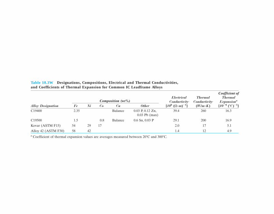
Table 18.3W Designations, Compositions, Electrical and Thermal Conductivities, and Coefficients of Thermal Expansion for Common IC Leadframe Alloys
Coefficient ofElectrical Thermal Thermal
Composition (wt%) Conductivity Conductivity Expansiona
Alloy Designation Fe Ni Co Cu Other [106 (�-m)�1] (W/m-K ) [10�6 (�C)�1]C19400 2.35 Balance 0.03 P, 0.12 Zn, 39.4 260 16.3
0.03 Pb (max)
C19500 1.5 0.8 Balance 0.6 Sn, 0.03 P 29.1 200 16.9
Kovar (ASTM F15) 54 29 17 2.0 17 5.1
Alloy 42 (ASTM F30) 58 42 1.4 12 4.9a Coefficient of thermal expansion values are averages measured between 20�C and 300�C.
wc18.26.qxd 0
5/16/2002 1
3:33 PM P
age 89

W-90
carried out at temperatures between 60�C (140�F) and 350�C (660�F) depending onthe application. Since the amounts of thermal expansion are different for the Cualloy leadframe plate and Si chip, the epoxy adhesive must be capable of absorb-ing any thermal strains produced during temperature changes such that the me-chanical integrity of the junction is maintained. Figure 18.11aW shows a schematicdiagram of a chip that is bonded to a substrate layer that is, in turn, bonded to theleadframe plate. Figure 18.11bW is a photograph of a chip, its leadframe, and theconnecting wires.
FIGURE 18.11W(a) Schematic diagram
showing the IC chip, itsattachment to the
substrate (or leadframeplate), and the
connecting wires thatrun to the leadframe
contact leads. [Adaptedfrom Electronic
Materials Handbook,Vol. 1, Packaging, C. A.
Dostal (Editor), ASMInternational, 1989,
p. 225.] (b) Photographshowing a portion of a
leadframe package.Included is the IC chip
along with itsconnecting wires. One
end of each wire isbonded to a chip pad;
the other wireextremity is bonded to
a leadframe contactlead. (Photograph
courtesy of NationalSemiconductor
Corporation.)
712�.
V
V
V
Wedge bond
Connecting wire
Ball bondContact pad
Chip (die)attachment
Substrate (optional)Leadframe plate
Leadframe
(a)
(b)
wc18.26.qxd 05/16/2002 13:33 PM Page 90

W-91
WIRE BONDINGThe next step in the packaging process involves making electrical connectionsbetween the metallized chip pads and the leadframe; this is accomplished usingconnecting wires (Figures 18.11aW and 18.11bW). A wire-bonding procedure isnormally carried out using a microjoining operation, since very fine wires are usedto make the connections. Wire bonding is the slow step in the packaging processbecause several hundred wires may need to be installed; this procedure is usuallyautomated.
Several important considerations must be taken into account relative to thechoice of wire alloy. Of course, a high electrical conductivity is the prime prerequi-site. In addition, consideration must be given to the ability of the alloy to bond, bywelding or brazing, with both the Al alloy at the chip pad and the Cu alloy on theleadframe; the formation of a microjoint that is both mechanically and electricallystable is an absolute necessity.
The most commonly used wire material is gold—actually a gold alloy contain-ing a small amount of beryllium–copper that is added to inhibit grain growth. Goldwires are round and have diameters that are typically 18 �m (0.0007 in.), 25 �m(0.001 in.), or 50 �m (0.002 in.). Less costly Cu and Al have also been employedfor contact wires. Prior to making the microjoint, regions of the chip pad and lead-frame surfaces at which the junctions are to be made may be coated with Au to im-prove bondability. During the actual microjoining process, one wire end is broughtinto the vicinity of one of the joint regions using a special tool. This wire end is thenmelted with a spark or flame heat source.
Two different types of microjoints are possible: ball and wedge. Figure 18.12Wis a schematic diagram showing a connecting wire having a ball microjoint at itscontact pad end and a wedge microjoint at the leadframe connection. Ball jointsare possible for gold wires since the melted wire end forms into a small ball be-cause of the high surface tension of gold. Bonding of this molten ball with the contactpad or leadframe is accomplished by making mechanical contact with the bondingsurface while both wire and surface are subjected to ultrasonic vibrations. A scan-ning electron micrograph of a ball microjoint is shown in Figure 18.13aW. This typeof microjoint is especially desirable since, after the first of the two microjoints foreach wire has been made (usually on the IC contact pad), the wire may then bebent in any direction in preparation for the microjoining of its other extremity.
The ends of copper and aluminum wires do not form balls upon melting. Theyare wedge microjoined by positioning the wire between a vibrating probe and thecontact pad or leadframe surface; the vibrations loosen and remove surfacecontaminants, which results in intimate contact of the two surfaces. An electriccurrent is then applied through the probe, which welds the wire to the surface.
FIGURE 18.12W Schematic diagramshowing a connecting wire that is ballbonded to the IC contact pad and wedgebonded to the leadframe. [Adapted fromElectronic Materials Handbook, Vol. 1,Packaging, C. A. Dostal (Editor), ASMInternational, 1989, p. 225.]
Connectingwire
Contactpad
Wedge bond(second bond)
Ball bond(first bond)
Leadframe
wc18.26.qxd 05/16/2002 13:33 PM Page 91

W-92
Unfortunately, the bending motion of wedge-bonded wires is restricted to a singledirection. Gold wires may also be bonded using wedge microjoints. Figure 18.13bWis a scanning electron micrograph of a wedge microjoint.
There are other considerations relative to wire bonding that deserve mention-ing. Microjunction alloy combinations that form intermetallic phases should beavoided because these phases are normally brittle and yield microjoints lackinglong-term mechanical stability. For example, Au and Al may react at elevated tem-peratures to form AuAl2, termed the “purple plague”; this compound is not onlyvery brittle (and purple), but also highly electrically resistive. Furthermore, me-chanical integrity at each microjoint is important to (1) withstand vibrations thatthe package may experience, and (2) survive thermal stresses that are generated asthe packaging materials change temperature.
PACKAGE ENCAPSULATIONThe microelectronic package, as now constituted, must be provided some type ofprotection from corrosion, contamination, and damage during handling and whilein service. The wire interconnection microjunctions are extremely fragile and maybe easily damaged. Especially vulnerable to corrosion are the narrow Al circuitpaths that have been metallized onto the surface of the IC chip; even the slightestcorrosion of these elements will impair the operation of the chip.These Al-metallizedlayers experience corrosion when atmospheric moisture in which even minute con-centrations of ionic contaminants are dissolved (especially chlorine and phosphorus)condenses on the chip surface. Furthermore, the corrosive reactions are acceleratedas a consequence of electric currents that pass through these circuit paths. In addi-tion, any sodium (as Na�) that gets on the chip surface will eventually diffuse intothe chip and destroy its operation.
FIGURE 18.13W Scanning electron micrographs of (a) a ball bond (475�), and(b) a wedge bond (275�). (Photographs courtesy of National SemiconductorCorporation.)
(b)(a)
wc18.26.qxd 05/16/2002 13:33 PM Page 92

W-93
The material used to encapsulate the package should:
1. Be electrically insulating
2. Be easily molded to the desired shape around the chip die and its wire leads
3. Be highly impervious to the penetration of moisture and contaminants
4. Be able to form strong adhesive bonds with the chip surface, wires, and otherleadframe components
5. Exhibit mechanical and chemical stability for the expected lifetime of thepackage
6. Not require exposure to excessively high temperatures during installation
7. Have a coefficient of thermal expansion similar to those of other pack-age components to avoid thermal stresses capable of fracturing the wire leads
Figure 18.14W shows a schematic diagram of an encapsulated IC package.Both ceramic and polymeric materials are used to encapsulate IC packages; of
course each of these material types has its own set of assets and liabilities. Ceram-ics are extremely resistant to moisture penetration and are chemically stable andchemically inert. Glasses are the most commonly utilized ceramic materials. Theprincipal disadvantage of glass is the requirement that it be heated to moderatelyhigh temperatures to lower its viscosity to the point where it will flow around andmake intimate contact with all of the wires that are microjoined to the chip surface.Some common glass constituents should be avoided (notably Na2O and K2O) sincevolatile cation species (Na� and K�) may be emitted from the molten glass. Thesespecies are notorious in accelerating corrosion reactions, and the ions will degradethe chip performance.
Polymeric materials are used in the largest volume for packaging encapsulationbecause they are not as costly as the ceramics, and they may be produced in a low-viscosity state at lower temperatures. Epoxies and polyurethanes are commonlyused, with the former being the most common. However, these materials have atendency to absorb water and do not form moisture-tight bonds with the lead wires.Some of these polymers require curing at a temperature on the order of 150�C, andduring cooling to room temperature will shrink more than other package compo-nents to which they are attached. This difference in amounts of contraction can giverise to mechanical strains of sufficient magnitude to damage the connecting wires
IC chip Encapsulation
Connectingwire
Encapsulation Leadframe
FIGURE 18.14W Schematicdiagram showing an encapsulatedIC leadframe package. [Adaptedfrom Electronic MaterialsHandbook, Vol. 1, Packaging, C.A. Dostal (Editor), ASMInternational, 1989, p. 241.]
wc18.26.qxd 05/16/2002 13:33 PM Page 93

W-94
as well as other electronic components. The addition of appropriate fillers (such asfine silica or alumina particles) to the polymer can alleviate this problem but oftenhas undesirable electrical consequences. A comparison of the important encapsu-lation characteristics of four different polymer types is given in Table 18.4W.
TAPE AUTOMATED BONDINGAnother packaging design, tape automated bonding (or TAB), a variation of theleadframe discussed above, has found widespread use by virtue of its low cost. Thetape-bonded package consists of a thin and flexible polyimide polymer backing filmsubstrate; onto this substrate surface is patterned an array of copper “finger” high-conductivity conduction paths similar in configuration to the contact leads for theconventional leadframe. A schematic diagram of a tape-bonded film leadframe isshown in Figure 18.15W.
IC
Sprocketdrive hole
Copper fingerinner lead(bonded to IC)
Outerlead
Window in polymer film —to expedite outer lead bonding
Polymer (polyimide) film
FIGURE 18.15WSchematic diagram of a
complete tape-bonded(TAB) leadframe.[From Electronic
Materials Handbook,Vol. 1, Packaging, C. A.
Dostal (Editor), ASMInternational, 1989,
p. 233.]
Table 18.4W Property Comparisons of Four Classes of Polymers Usedfor IC Package Encapsulation
Epoxy Resins Silicones Polyurethanes PolysulphidesDielectric strength Good Good Good GoodElastic modulus High Low Wide range LowTensile strength High Low Wide range —Precursor viscosity Low Low Low HighAdhesion to package Excellent Poor Good Good
(to ceramics)Moisture diffusion rate High High Low Very low
Source: From C. R. M. Grovenor, Microelectronic Materials.Copyright © 1989 by Institute of Physics Publishing, Bristol, England.
wc18.26.qxd 05/16/2002 13:34 PM Page 94

W-95
Mechanical support for the assembly is provided by the polyimide film, ontowhich the die is bonded using an adhesive. Polyimide strip widths are typically35 mm (1.38 in.), and sprocket holes are incorporated along opposing edges tofacilitate movement and positioning of the TAB leadframes. Literally thousandsof these individual units, attached end to end, are spooled onto reels in prepara-tion for automated processing.
The copper fingers are extremely narrow and positioned close together. Sep-aration distances of the inner contact leads are on the order of 50 �m, which ismuch smaller than is possible for the stamped leadframe. Furthermore, each diechip contact pad is microjoined directly to one of these copper fingers, whicheliminates the need for any connecting wires. The copper fingers are very thin,so that, for this direct bonding to be achieved, the chip pad bonding sites mustbe raised above the metallized coating. This is accomplished using “solderbumps,” which are normally layers of gold (or gold-plated copper) approximately25 �m thick. Schematic representations illustrating this attachment design arepresented in Figure 18.16W. The finger contacts are bonded to these raised bumpsby soldering using a thermal-compression bonding tool. This tape-bonding de-sign is fully automated in that all of the hundred or so microjoints can be madein a single step, a feature not possible with leadframes that require multiple wire-bonding operations.
The packaging operation for the TAB leadframe is completed, as with thestamped leadframe, by encapsulation of the assembly (i.e., tape leadframe and its at-tached chip) within a fluid polymeric material that subsequently cures to form a pro-tective shield. Protruding from this package are the copper finger conducting pathsto which external electrical connections are made. Furthermore, excess heat gener-ated by the chip must be dissipated along these copper fingers since the polymer
FIGURE 18.16WSchematic diagrams
showing (a) the crosssection of an
encapsulated TABleadframe package, and
(b) how bondingbetween the IC chip
and a copper finger isachieved with a solderbump. [Adapted from
Electronic MaterialsHandbook, Vol. 1,
Packaging, C. A. Dostal(Editor), ASM
International, 1989, pp.233, 234.]
Polymer film Encapsulation Solder bump
Leadframe finger
Solder joint
Die attachment
IC chip
(a)
Leadframe plateor substrate
Copper finger
Gold layer
Contact pad
Passivationlayer
Solder bump
IC chip
(b)
Polymerfilm
wc18.26.qxd 05/16/2002 13:34 PM Page 95

W-96
tape backing does not provide an effective thermal conduction path because of itslow thermal conductivity.
The ultimate design goal of the IC package is to allow for the proper elec-trical operation of the packaged device. As frequencies and computing speedscreep ever higher, the mechanical and electrical design considerations of thepackage design must become more and more integrated. The overall electricalperformance of the package is as important to the end user as the overallreliability.
wc18.26.qxd 05/16/2002 13:34 PM Page 96

W-97
C h a p t e r 19 / Thermal Properties
C A S E S T U D Y19.6W THERMAL PROTECTION SYSTEM ON
THE SPACE SHUTTLE ORBITER
Illustrative examples of materials and materials systems that have been designedwith very specific and well-defined thermal characteristics are provided by this casestudy, which examines the thermal protection system for the Space Shuttle Orbiter.
INTRODUCTIONIn 1969, the National Aeronautics and Space Administration (NASA) of the UnitedStates decided to direct its primary mission to the development of a Space Trans-portation System (STS), also commonly known as the Space Shuttle Orbiter. Inessence, the Space Shuttle is a reusable cargo-carrying space vehicle that is launchedaboard a rocket and then orbits the earth. Upon mission completion, it reenters theatmosphere as a space craft and, finally, once inside the lower atmosphere, lands inthe manner of a normal aircraft. The maiden flight was made by the Columbiaorbiter in April of 1981; since then, four other orbiters have been constructed—Discovery, Atlantis, Endeavour, and the ill-fated Challenger.
The successful operation of the Space Shuttle is dependent on a fully reusableouter “skin,” termed a Thermal Protection System (TPS), that protects the inner air-frame and its occupants from the searing heat generated during the reentry phasefrom space into the earth’s atmosphere. The development of this Thermal Protec-tion System evolved over a 20-year period, and is a classical and somewhat involvedmaterials selection and design problem. In this section the primary components ofthe Shuttle’s TPS are discussed.
In reading this section, keep in mind that cost constraints relative to the designand fabrication of these materials were not as rigid as would be expected for normalcommercial applications.
THERMAL PROTECTION SYSTEM—DESIGN REQUIREMENTSMaterial requirements on the Thermal Protection System are, to say the least,awesome. For example, the TPS must do the following:
1. Maintain the temperature on the inner airframe below that to which it wasdesigned [viz., 175�C (350�F)] for a maximum outer surface temperature of1260�C (2300�F)
2. Remain usable for 100 missions, with a maximum turnaround time of 160 h
3. Provide and maintain an aerodynamically smooth outer surface
4. Be constructed of low-density materials
wc19.6.qxd 05/16/2002 13:34 PM Page 97

W-98
5. Withstand temperature extremes between �110�C (�170�F) and 1260�C(2300�F)
6. Be resistant to severe thermal gradients and rapid temperature changes
7. Be able to withstand stresses and vibrations that are experienced during launch,as well as thermally induced stresses imposed during temperature changes
8. Experience a minimum absorption of moisture and other contaminants dur-ing storage between missions
9. Be made to adhere to the airframe that is constructed of an aluminum alloy
Thermal protection systems and materials developed previously by the aero-space industry proved unsuitable for the Space Shuttle because they were eithertoo dense and/or nonreusable. Therefore, it became necessary to design a new setof complex materials. Furthermore, no single material is capable of meeting all ofthe criteria listed above. In addition, not all of these criteria are required over allsurfaces of the spacecraft; for example, typical reentry maximum temperature pro-files are shown in Figure 19.1W.
Lower surfaceview
Upper surfaceview
1260°C
980°C
650°C425°C
1095°C
315°C
650°C
400°C
1350°C
1500°C
1095°C
1260°C
980°C
1260°C
(a)
650°C
1465°C
425°C
1095°C
315°C
425°C
400°C
650°C
955°C
1175°C
540°C
445°C
Side surface view(b)
FIGURE 19.1W Approximate maximum outer surface temperature profiles forthe Space Shuttle Orbiter during reentry: (a) upper and lower views; (b) side view.(From “The Shuttle Orbiter Thermal Protection System,” L. J. Korb, C. A. Morant,R. M. Calland, and C. S. Thatcher, Ceramic Bulletin, No. 11, Nov. 1981, p. 1188.Copyright 1981. Reprinted by permission of the American Ceramic Society.)
wc19.6.qxd 05/16/2002 13:34 PM Page 98

W-99
Table 19.1W Thermal Protection Systems Employed on the Space Shuttle Orbiter
Minimum MaximumOperating Operating
Temperature, Temperature, Material OrbiterMaterial Generic Name �C (�F) �C (�F) Composition LocationsFelt reusable surface �130 400 Nylon felt, silicone Wing upper surface,
insulation (FRSI) (�200) (750) rubber coating upper sides, cargobay doors
Advanced flexible �130 815 Quartz batting sandwiched Upper surface regionsreusable surface (�200) (1500) between quartz andinsulation (AFRSI) glass fabrics
Low-temperature �130 650 Silica tiles, borosilicate Upper wing surfaces,reusable surface (�200) (1200) glass coating tail surfaces, upperinsulation (LRSI) vehicle sides
High-temperature �130 1260 Silica tiles, borosilicate Lower surfaces and reusable insulation (�200) (2300) glass coating with SiB4 sides, tail leading and(HRSI) added trailing edges
Reinforced carbon– No lower 1650 Pyrolized carbon–carbon, Nose cap and wingcarbon (RCC) limit (3000) coated with SiC leading edges
identified
Source: Adapted from L. J. Korb, C. A. Morant, R. M. Calland, and C. S. Thatcher, “The Shuttle Orbiter ThermalProtection System,” Ceramic Bulletin, No. 11, Nov. 1981, p. 1188. Copyright 1981. Reprinted by permission of theAmerican Ceramic Society.
Therefore, the philosophy adopted was to design several different thermal pro-tection materials systems, each with its particular set of properties, that satisfy therequired criteria for a specific region of the spacecraft surface. Several different ma-terials systems are employed on the Space Shuttles, the designs of which dependon the maximum outer surface temperature generated during vehicle reentry.Thesesystems and their temperature ranges of operation, material compositions, andorbiter areas are listed in Table 19.1W. Furthermore, the locations of these varioussystems are indicated in Figure 19.2W.
THERMAL PROTECTION SYSTEM—COMPONENTSFelt Reusable Surface InsulationUpper surface regions exposed up to temperatures of 400�C (750�F) are coveredwith what is termed felt reusable surface insulation (FRSI). This insulation con-sists of felt blankets of a nylon material the outer surface of which is coated witha silicone elastomer to achieve the necessary surface thermal properties. Theseblankets come in two thicknesses, 4 and 8 mm (0.16 and 0.32 in.), and are bondedto the aluminum airframe by a room-temperature vulcanizing (RTV) siliconeadhesive.
Other upper surface regions that are exposed to higher temperatures, not toexceed 815�C (1500�F), are protected by blankets of an advanced flexible reusablesurface insulation (AFRSI). These blankets consist of a quartz fiber batting that issandwiched between a high-temperature woven quartz fabric on the outer side anda lower-temperature glass fabric on the inner side. The outer surface of some re-gions is also protected with a ceramic coating. Furthermore, these three layers arestitched together using quartz and glass threads in a one-inch square pattern.AFRSIblanket thicknesses range between 10 mm (0.41 in.) and just under 50 mm (2 in.).
wc19.6.qxd 05/16/2002 13:34 PM Page 99
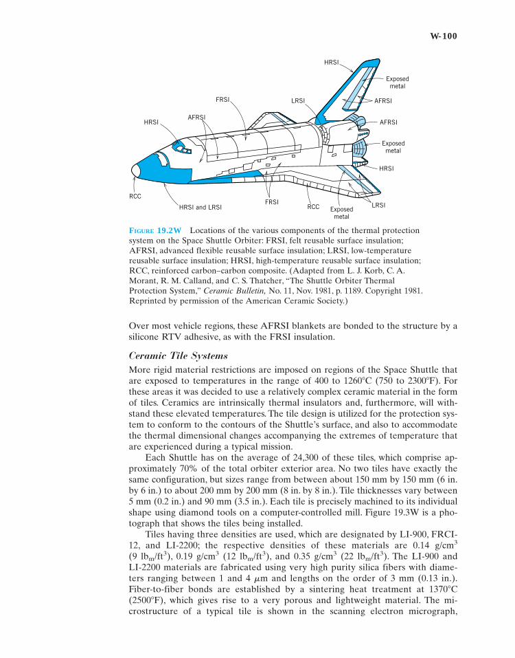
W-100
Over most vehicle regions, these AFRSI blankets are bonded to the structure by asilicone RTV adhesive, as with the FRSI insulation.
Ceramic Tile SystemsMore rigid material restrictions are imposed on regions of the Space Shuttle thatare exposed to temperatures in the range of 400 to 1260�C (750 to 2300�F). Forthese areas it was decided to use a relatively complex ceramic material in the formof tiles. Ceramics are intrinsically thermal insulators and, furthermore, will with-stand these elevated temperatures. The tile design is utilized for the protection sys-tem to conform to the contours of the Shuttle’s surface, and also to accommodatethe thermal dimensional changes accompanying the extremes of temperature thatare experienced during a typical mission.
Each Shuttle has on the average of 24,300 of these tiles, which comprise ap-proximately 70% of the total orbiter exterior area. No two tiles have exactly thesame configuration, but sizes range from between about 150 mm by 150 mm (6 in.by 6 in.) to about 200 mm by 200 mm (8 in. by 8 in.). Tile thicknesses vary between5 mm (0.2 in.) and 90 mm (3.5 in.). Each tile is precisely machined to its individualshape using diamond tools on a computer-controlled mill. Figure 19.3W is a pho-tograph that shows the tiles being installed.
Tiles having three densities are used, which are designated by LI-900, FRCI-12, and LI-2200; the respective densities of these materials are 0.14 g/cm3
(9 lbm/ft3), 0.19 g/cm3 (12 lbm/ft3), and 0.35 g/cm3 (22 lbm/ft3). The LI-900 andLI-2200 materials are fabricated using very high purity silica fibers with diame-ters ranging between 1 and 4 �m and lengths on the order of 3 mm (0.13 in.).Fiber-to-fiber bonds are established by a sintering heat treatment at 1370�C(2500�F), which gives rise to a very porous and lightweight material. The mi-crostructure of a typical tile is shown in the scanning electron micrograph,
FIGURE 19.2W Locations of the various components of the thermal protectionsystem on the Space Shuttle Orbiter: FRSI, felt reusable surface insulation;AFRSI, advanced flexible reusable surface insulation; LRSI, low-temperaturereusable surface insulation; HRSI, high-temperature reusable surface insulation;RCC, reinforced carbon–carbon composite. (Adapted from L. J. Korb, C. A.Morant, R. M. Calland, and C. S. Thatcher, “The Shuttle Orbiter ThermalProtection System,” Ceramic Bulletin, No. 11, Nov. 1981, p. 1189. Copyright 1981.Reprinted by permission of the American Ceramic Society.)
HRSI and LRSIFRSI
RCC Exposedmetal
LRSI
AFRSI
Exposedmetal
AFRSI
HRSI
LRSI
HRSI
FRSI
AFRSIHRSI
RCC
Exposedmetal
wc19.6.qxd 05/16/2002 13:34 PM Page 100

W-101
Figure 19.4W. On the other hand, FRCI tiles are composed of a 78% silicafiber–22% aluminum borosilicate fiber composite; the FRCI designation comesfrom Fibrous Refractory Composite Insulation.
The strengths of the LI-2200 and FRCI tiles are virtually equivalent, beinggreater than that of LI-900. LI-2200 and FRCI are used in those locations where ahigher strength is required, such as around doors and access panels. Employmentof FRCI instead of LI-2200 reduced orbiter weight by approximately 450 kg (1000lbm). Most tiles on the orbiters are the LI-900 type.
These low-density silica fiber materials are ideal for the Shuttle’s Thermal Pro-tection System. Being approximately 93 vol% void, they are excellent thermalinsulators; this is confirmed by the photograph on page 656, which shows a manholding a very hot cube of the tile material in his bare hands. Furthermore, silicahas an extremely low coefficient of thermal expansion (Table 19.1) as well as a rel-atively small modulus of elasticity (Table 12.5); thus, it is very resistant to thermal
FIGURE 19.3W Photograph showingthe installation of thermal protectionceramic tiles on the Space ShuttleOrbiter. [Photograph courtesy theNational Aeronautics and SpaceAdministration (NASA).]
FIGURE 19.4W Scanningelectron micrograph of aSpace Shuttle Orbiterceramic tile showing silicafibers that were bonded toone another during asintering heat treatment.750�. (Photograph providedcourtesy of LockheedAerospace CeramicsSystems, Sunnyvale,California.)
wc19.6.qxd 05/16/2002 13:34 PM Page 101

W-102
shock associated with rapid temperature changes (Equation 19.8). Also, silica maybe heated to relatively high temperatures without softening; short-term exposuresto temperatures as high as 1480�C (2700�F) are possible.
The properties of the tiles are anisotropic; they are designed to be strongest inthe plane of the tile and to be most thermally insulative in the direction perpendi-cular to this plane.
Tiles on surfaces exposed to maximum temperatures in the range of 400 to 650�C(750 to 1200�F) (i.e., upper vehicle sides, and upper wing and tail surfaces) are coatedwith a thin layer (0.30 mm [0.012 in.] thick) of a high-emittance borosilicate glass.This tile type is referred to as a low-temperature reusable surface insulation (LRSI);the tile surface is white, which reflects the sun’s rays and keeps the Shuttle relativelycool while in orbit. Locations of the LRSI tiles are indicated in Figure 19.2W.
Those tiles that are exposed to higher maximum temperatures between 650�C(1200�F) and 1260�C (2300�F) (i.e., the vehicle underbody, and tail leading and trail-ing edges) receive a black coating consisting of the same borosilicate glass and, inaddition, silicon tetraboride (SiB4); this coating material is sometimes termed areaction cured glass (RCG). Being of high optical emittance, this coating is able toradiate approximately 90% of the reentry heat generated away from the Shuttle ei-ther into the earth’s atmosphere or into deep space. This type of tile is termed ahigh-temperature reusable surface insulation (HRSI), and its locations on the Shut-tle are also noted in Figure 19.2W.
It is also necessary to isolate and cushion the brittle ceramic tiles from the me-chanical and thermal strains sustained by the airframe and, in addition, to attachthe tiles to the airframe. This is accomplished by an assembly consisting of a strainisolator pad (SIP), a filler bar, and a silicone RTV adhesive that bonds the tile tothe SIP and the SIP and filler bar to the airframe structure. A schematic diagramof this assembly is shown in Figure 19.5W. The strain isolator pad is composed of anylon felt that will sustain repeated heatings to 290�C (550�F); this pad isolates thetiles from airframe deflections.
Beneath the tile-to-tile junctions are located the filler bars.They are of the samenylon felt to which an RTV outer coating has been applied. The thickness of these
Coatedtiles Gap
Strainisolatorpad
Adhesive
Filler bar
Airframe
FIGURE 19.5W Schematic cross section of the tile component of the SpaceShuttle Orbiter’s thermal protection system. (From L. J. Korb, C. A. Morant, R.M. Calland, and C. S. Thatcher, “The Shuttle Orbiter Thermal Protection System,”Ceramic Bulletin, No. 11, Nov. 1981, p. 1189. Copyright 1981. Reprinted bypermission of the American Ceramic Society.)
wc19.6.qxd 05/16/2002 13:34 PM Page 102

W-103
bars is greater than the strain isolator pad, and, as such, they form a gasket seal tothe undersurface of the tiles and protect the strain isolator pads from water orplasma penetration through the tile-to-tile junctions.
The adhesive that bonds this system together and to the airframe must surviverepeated exposures to at least 290�C (550�F), must cure at room temperature, andmust be capable of filling any irregularities in the airframe structure. The onlymaterial that fulfills all these requirements is a silicone RTV adhesive.
Reinforced Carbon–CarbonDuring reentry, some shuttle orbiter surface regions are exposed to temperaturesin excess of those that the ceramic tiles are capable of sustaining (1260�C [2300�F]).Specifically, these areas are the nose cap and wing leading edges, Figure 19.1W,where temperatures may reach as high as 1650�C (3000�F). The material that wasdesigned for use in these locations is a reinforced carbon–carbon (RCC) compos-ite. It is also a relatively complex material consisting of a carbon matrix that isreinforced with graphite fibers; the surface is coated with a thin layer of silicon car-bide (SiC) as a protection against oxidation. This composite material is suitable forthese high-temperature locations for the following reasons: strength and stiffnessare retained up to the maximum service temperatures; it has a low coefficient ofthermal expansion, and thus will not experience significant thermal stresses and de-flections; it is highly resistant to thermal shock and fatigue; its density is very low;and fabrication into complex shapes is possible. Figure 19.2W shows those areaswhere this RCC composite material is employed.
Of course, materials other than those already cited are used on the Orbiter. Forexample, window ports are made of glass materials. Also, as may be noted fromFigure 19.2W, metal alloys are used for some exposed surfaces. These alloys willtypically have high melting temperatures and, preferably, relatively low densities.Examples include beryllium, niobium, titanium, stainless steel (alloys 316), and sev-eral superalloys (Inconel alloys 718, 625, 750, and Haynes alloy 188).
wc19.6.qxd 05/16/2002 13:34 PM Page 103

W-104
Why Study Economic, Environmental, and Societal Issues inMaterials Science and Engineering?
It is essential for the engineer to know about andunderstand economic issues simply because thecompany/institution for which he or she worksmust realize a profit from the products it manufac-tures. Materials engineering decisions have eco-nomic consequences with regard to both materialand production costs.
An awareness of environmental and societalissues is important for the engineer because, overtime, greater demands are being made on the
world’s natural resources. Furthermore, levels ofpollution are ever increasing. Materials engineeringdecisions have impacts on the consumption of rawmaterials and energy, on the contamination of ourwater and atmosphere, and on the ability of the con-sumer to recycle or dispose of spent products. Thequality of life for this and future generations will de-pend, to some degree, on how these issues are ad-dressed by the global engineering community.
Used aluminum beverage
cans that are to be recycled.
These cans will be crushed
and pressed into bales (shown
in the background) and then
shredded into small pieces.
Ferrous and nonferrous metal
contaminants are next elimi-
nated, and the decorative
coating is removed in a
delacquering operation. A
thermomechanical process
then separates can bodies
(alloy 3004) from the lids
(alloy 5182). The final recy-
cling stages include melting, re-
fining, casting, and rolling.
(Photograph courtesy Alcoa.)
Chapter 22W / Economic, Environmental, andSocietal Issues in MaterialsScience and Engineering
c22.qxd 05/16/2002 14:39 PM Page 104

W-105
22.1W INTRODUCTION
In previous chapters, we dealt with a variety of materials science and materialsengineering issues to include criteria that may be employed in the materials selectionprocess. Many of these selection criteria relate to material properties or propertycombinations—mechanical, electrical, thermal, corrosion, etc.; the performance ofsome component will depend on the properties of the material from which it ismade. Processability or ease of fabrication of the component may also play a rolein the selection process. Virtually all of this book, in one way or another, hasaddressed these property and fabrication issues.
In engineering practice there are other important criteria that must be consid-ered in the development of a marketable product. Some of these are economic innature, which, to some degree, are unrelated to scientific principles and engineeringpractice, and yet are significant if a product is to be competitive in the commercialmarketplace. Other criteria that should be addressed involve environmental andsocietal issues such as pollution, disposal, recycling, and energy. This final chapteroffers relatively brief overviews of economic, environmental, and societal consid-erations that are important in engineering practice.
E C O N O M I C C O N S I D E R AT I O N SIt goes without saying that engineering practice involves utilizing scientific princi-ples to design components and systems that perform reliably and satisfactorily. An-other critical driving force in engineering practice is that of economics; simply stated,the company or institution must realize a profit from the products that it manu-factures and sells. The engineer might design the perfect component; however, asmanufactured, it must be offered for sale at a price that is attractive to the con-sumer and, in addition, return a suitable profit to the company. Only a brief overviewof important economic considerations as they apply to the materials engineer willbe provided. The student may want to consult references provided at the end ofthis chapter that address engineering economics in detail.
There are three factors over which the materials engineer has control and thataffect the cost of a product; they are (1) component design, (2) the material(s) used,and (3) the manufacturing technique(s) that are employed. These factors are inter-related in that component design may affect which material is used, and bothcomponent design and the material used will influence the choice of manufacturingtechnique(s). Economic considerations for each of these factors is now brieflydiscussed.
L e a r n i n g O b j e c t i v e sAfter careful study of this chapter you should be able to do the following:
4. Cite issues that are relevant to the “green de-sign” philosophy of product design.
5. Discuss recyclability/disposability issues relativeto (a) metals, (b) glass, (c) plastics and rubber,and (d) composite materials.
1. List and briefly discuss three factors over whichan engineer has control that affect the cost of aproduct.
2. Diagram the total materials cycle, and brieflydiscuss relevant issues that pertain to each stageof this cycle.
3. List the two inputs and five outputs for the lifecycle analysis/assessment scheme.
c22.qxd 05/16/2002 14:39 PM Page 105

W-106
22.2W COMPONENT DESIGN
Some fraction of the cost of a component is associated with its design. In this con-text, component design is the specification of size, shape, and configuration, whichwill affect in-service component performance. For example, if mechanical forces arepresent, then stress analyses may be required. Detailed drawings of the componentmust be prepared; computers are normally employed, using software that has beengenerated for this specific function.
It is often the case that a single component is part of a complex device or sys-tem consisting of a large number of components (e.g., the television, automobile,VCR, etc.). Thus, design must take into consideration each component’s contribu-tion to the efficient operation of the complete system.
Component design is a highly iterative process that involves many compromisesand trade-offs.The engineer should keep in mind that an optimal component designmay not be possible due to system constraints.
22.3W MATERIALS
In terms of economics, we want to select the material or materials with the appro-priate combination(s) of properties that are the least expensive. Once a family ofmaterials has been selected that satisfy the design constraints, cost comparisons ofthe various candidate materials may be made on the basis of cost per part. Mater-ial price is usually quoted per unit mass. The part volume may be determined fromits dimensions and geometry, which is then converted into mass using the densityof the material. In addition, during manufacturing there ordinarily is some un-avoidable material waste, which should also be taken into account in these com-putations. Current prices for a wide variety of engineering materials are containedin Appendix C.
22.4W MANUFACTURING TECHNIQUES
As already stated, the choice of manufacturing process will be influenced by boththe material selected and part design. The entire manufacturing process will nor-mally consist of primary and secondary operations. Primary operations are thosethat convert the raw material into a recognizable part (e.g., casting, plastic forming,powder compaction, molding, etc.), whereas secondary ones are those subsequentlyemployed to produce the finished part (e.g., heat treatments, welding, grinding,drilling, painting, decorating). The major cost considerations for these processes in-clude capital equipment, tooling, labor, repairs, machine downtime, and waste. Ofcourse, within this cost analysis, rate of production is an important consideration.If this particular part is one component of a system, then assembly costs must alsobe addressed. Finally, there will undoubtedly be costs associated with inspection andpackaging of the final product.
As a sidelight, there are also other factors not directly related to design, material,or manufacturing that figure into the product selling price. These factors include la-bor fringe benefits, supervisory and management labor, research and development,property and rent, insurance, profit, taxes, and so on.
c22.qxd 05/16/2002 14:39 PM Page 106
W-107
E N V I R O N M E N TA L A N D S O C I E TA LC O N S I D E R AT I O N S
Our modern technologies and the manufacturing of their associated products im-pact our societies in a variety of ways—some are positive, others are adverse. Fur-thermore, these impacts are economic and environmental in type, and internationalin scope inasmuch as (1) the resources required for a new technology often comefrom many different countries, (2) the economic prosperity resulting from techno-logical development is global in extent, and (3) environmental impacts may extendbeyond the boundaries of a single country.
Materials play a crucial role in this technology-economy-environment scheme.A material that is utilized in some end product and then discarded passes throughseveral stages or phases; these stages are represented in Figure 22.1W, which issometimes termed the “total materials cycle” or just “materials cycle,” and repre-sents the “cradle-to-grave” life circuit of a material. Beginning on the far left sideof Figure 22.1W, raw materials are extracted from their natural earthly habitats bymining, drilling, harvesting, and so on.These raw materials are then purified, refined,and converted into bulk forms such as metals, cements, petroleum, rubber, and fibers.Further synthesis and processing results in products that are what may be termed“engineered materials”; examples include metal alloys, ceramic powders, glass, plas-tics, composites, semiconductors, and elastomers. Next, these engineered materialsare further shaped, treated, and assembled into products, devices, and appliancesthat are ready for the consumer—this constitutes the “product design, manufacture,assembly” stage of Figure 22.1W. The consumer purchases these products and usesthem (the “applications” stage) until they wear out or become obsolete, and are
FIGURE 22.1W Schematic representation of the total materials cycle. (Adaptedfrom M. Cohen, Advanced Materials & Processes, Vol. 147, No. 3, p. 70, 1995.Copyright © 1995 by ASM International. Reprinted by permission of ASMInternational, Materials Park, OH.)
Rawmaterials
Recycle/reuse
Waste
Engineeredmaterials
Product design,manufacture,
assembly
Applications
Agriculture • ConstructionEnvironmental • Defense
Information/CommunicationsTransportation • Energy • Health
Extraction/Production
Synthesisand
processing
c22.qxd 05/16/2002 14:39 PM Page 107
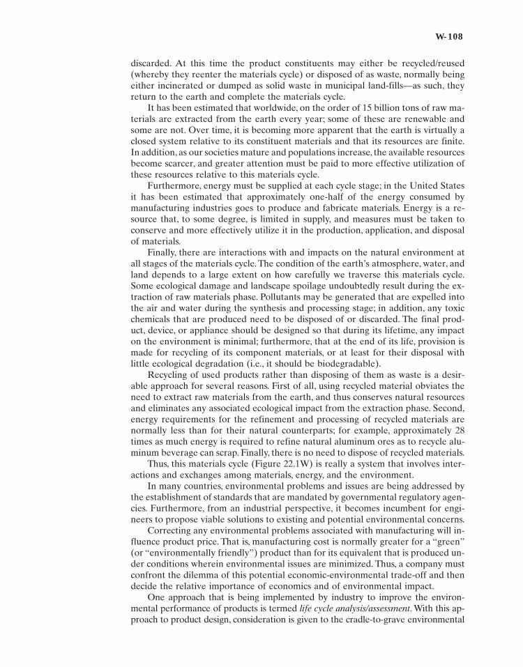
W-108
discarded. At this time the product constituents may either be recycled/reused(whereby they reenter the materials cycle) or disposed of as waste, normally beingeither incinerated or dumped as solid waste in municipal land-fills—as such, theyreturn to the earth and complete the materials cycle.
It has been estimated that worldwide, on the order of 15 billion tons of raw ma-terials are extracted from the earth every year; some of these are renewable andsome are not. Over time, it is becoming more apparent that the earth is virtually aclosed system relative to its constituent materials and that its resources are finite.In addition, as our societies mature and populations increase, the available resourcesbecome scarcer, and greater attention must be paid to more effective utilization ofthese resources relative to this materials cycle.
Furthermore, energy must be supplied at each cycle stage; in the United Statesit has been estimated that approximately one-half of the energy consumed bymanufacturing industries goes to produce and fabricate materials. Energy is a re-source that, to some degree, is limited in supply, and measures must be taken toconserve and more effectively utilize it in the production, application, and disposalof materials.
Finally, there are interactions with and impacts on the natural environment atall stages of the materials cycle. The condition of the earth’s atmosphere, water, andland depends to a large extent on how carefully we traverse this materials cycle.Some ecological damage and landscape spoilage undoubtedly result during the ex-traction of raw materials phase. Pollutants may be generated that are expelled intothe air and water during the synthesis and processing stage; in addition, any toxicchemicals that are produced need to be disposed of or discarded. The final prod-uct, device, or appliance should be designed so that during its lifetime, any impacton the environment is minimal; furthermore, that at the end of its life, provision ismade for recycling of its component materials, or at least for their disposal withlittle ecological degradation (i.e., it should be biodegradable).
Recycling of used products rather than disposing of them as waste is a desir-able approach for several reasons. First of all, using recycled material obviates theneed to extract raw materials from the earth, and thus conserves natural resourcesand eliminates any associated ecological impact from the extraction phase. Second,energy requirements for the refinement and processing of recycled materials arenormally less than for their natural counterparts; for example, approximately 28times as much energy is required to refine natural aluminum ores as to recycle alu-minum beverage can scrap. Finally, there is no need to dispose of recycled materials.
Thus, this materials cycle (Figure 22.1W) is really a system that involves inter-actions and exchanges among materials, energy, and the environment.
In many countries, environmental problems and issues are being addressed bythe establishment of standards that are mandated by governmental regulatory agen-cies. Furthermore, from an industrial perspective, it becomes incumbent for engi-neers to propose viable solutions to existing and potential environmental concerns.
Correcting any environmental problems associated with manufacturing will in-fluence product price. That is, manufacturing cost is normally greater for a “green”(or “environmentally friendly”) product than for its equivalent that is produced un-der conditions wherein environmental issues are minimized. Thus, a company mustconfront the dilemma of this potential economic-environmental trade-off and thendecide the relative importance of economics and of environmental impact.
One approach that is being implemented by industry to improve the environ-mental performance of products is termed life cycle analysis/assessment. With this ap-proach to product design, consideration is given to the cradle-to-grave environmental
c22.qxd 05/16/2002 14:39 PM Page 108

W-109
assessment of the product, from material extraction to product manufacture to productuse, and, finally, to recycling and disposal; sometimes this approach is also labeled“green design.” One important phase of this approach is to quantify the various inputs(e.g., materials and energy) and outputs (e.g., wastes) for each phase of the life cycle;this is represented schematically in Figure 22.2W. In addition, an assessment is con-ducted relative to the impact on both global and local environments in terms of theeffects on the ecology, human health, and resource reserves.
22.5W RECYCLING ISSUES IN MATERIALS SCIENCE
AND ENGINEERING
Important stages in the materials cycle where materials science and engineeringplays a significant role are recycling and disposal. The issues of recyclability and dis-posability are important when new materials are being designed and synthesized.Furthermore, during the materials selection process, the ultimate disposition of thematerials employed should be an important criterion. Let us conclude this sectionby briefly discussing several of these recyclability/disposability issues.
From an environmental perspective, the ideal material should be either totallyrecyclable or completely biodegradable. Recyclable means that a material, after hav-ing completed its life cycle in one component, could be reprocessed, could reenterthe materials cycle, and could be reused in another component—a process that couldbe repeated an indefinite number of times. By completely biodegradable, we meanthat, by interactions with the environment (natural chemicals, microorganisms, oxy-gen, heat, sunlight, etc.), the material deteriorates and returns to virtually the samestate in which it existed prior to the initial processing. Engineering materials exhibitvarying degrees of recyclability and biodegradability.
METALSMost metal alloys (e.g., Fe, Cu), to one degree or another experience corrosion andare also biodegradable. However, some metals (e.g., Hg, Pb) are toxic and, whenland-filled, may present health hazards. Furthermore, alloys of most metals are re-cyclable; on the other hand it is not feasible to recycle all alloys of every metal. Inaddition, the quality of alloys that are recycled tends to diminish with each cycle.
FIGURE 22.2WSchematic
representation of aninput/output inventory
for the life-cycleassessment of a
product. (Adapted fromJ. L. Sullivan and S. B.
Young, AdvancedMaterials & Processes,
Vol. 147, No. 2, p. 38,1995. Copyright © 1995by ASM International.
Reprinted bypermission of ASM
International, MaterialsPark, OH.)
INPUTS
Energy
Rawmaterials
Materials production
Product manufacturing
Product use
Product disposal
OUTPUTS
Usable products
Water effluents
Air emissions
Solid wastes
Other impacts
c22.qxd 05/16/2002 14:39 PM Page 109

W-110
Product designs should allow for the dismantling of components composed ofdifferent alloys. Another of the problems of recycling involves separation of vari-ous alloys types (e.g., aluminum from ferrous alloys) after dismantling and shred-ding; in this regard, some rather ingenious separation techniques have been devised(e.g., magnetic and gravity). Joining of dissimilar alloys presents contamination prob-lems; for example, if two similar alloys are to be joined, welding is preferred overbolting or riveting. Coatings (paints, anodized layers, claddings, etc.) may also actas contaminants, and render the material nonrecyclable.
Aluminum alloys are very corrosion resistant and, therefore, nonbiodegradable.Fortunately, however, they may be recycled; in fact, aluminum is the most impor-tant recyclable nonferrous metal. Since aluminum is not easily corroded, it may betotally reclaimed. A low ratio of energy is required to refine recycled aluminumrelative to its primary production. In addition, there are a large number of com-mercially available alloys that have been designed to accommodate impurity con-tamination. The primary sources of recycled aluminum are used beverage cans andscrapped automobiles.
GLASSThe one ceramic material that is consumed by the general public in the greatestquantities is glass, in the form of containers. Glass is a relatively inert material, and,as such, it does not decompose; thus, it is not biodegradable. A significant propor-tion of municipal land-fills consists of waste glass; so also does incinerator residue.
In addition, there is not a significant economic driving force for recycling glass.Its basic raw materials (sand, soda ash, and limestone) are inexpensive and readilyavailable. Furthermore, salvaged glass (also called “cullet”) must be sorted by color(clear, amber, and green), by type (plate versus container), and by composition (lime,lead, and borosilicate [or Pyrex]); these sorting procedures are time-consuming andexpensive. Therefore, scrap glass has a low market value, which diminishes its re-cyclability. Advantages of utilizing recycled glass include more rapid and increasedproduction rates and a reduction in pollutant emissions.
PLASTICS AND RUBBEROne of the reasons that synthetic polymers (including rubber) are so popular as en-gineering materials lies with their chemical and biological inertness. On the downside, this characteristic is really a liability when it comes to waste disposal. Polymersare not biodegradable, and, as such, they constitute a significant land-fill compo-nent; major sources of waste are from packaging, junk automobiles, automobile tires,and domestic durables. Biodegradable polymers have been synthesized, but theyare relatively expensive to produce. On the other hand, since some polymers arecombustible and do not yield appreciable toxic or polluting emissions, they may bedisposed of by incineration.
Thermoplastic polymers, specifically polyethylene terephthalate, polyethylene,and polypropylene, are those most amenable to reclamation and recycling, sincethey may be reformed upon heating. Sorting by type and color is necessary. In theUnited States, type sorting of packaging materials is facilitated using a number iden-tification code; for example, a “1” denotes high-density polyethylene (HDPE). Table22.1W presents these recycling code numbers and their associated materials. Alsoincluded in the table are uses of virgin and recycled materials. Plastics recycling iscomplicated by the presence of fillers (Section 15.21) that were added to modifythe original properties. The recycled plastic is less costly than the original material,and quality and appearance are generally degraded with each recycle. Typical
c22.qxd 05/16/2002 14:39 PM Page 110

applications for recycled plastics include shoe soles, tool handles, and industrialproducts such as pallets.
The recycling of thermoset resins is much more difficult since these materialsare not easily remolded or reshaped due to their crosslinked or network structures.Some thermosets are ground up and added to the virgin molding material prior toprocessing; as such, they are recycled as filler materials.
Rubber materials present some disposal and recycling challenges. When vul-canized, they are thermoset materials, which makes chemical recycling difficult. Inaddition, they may also contain a variety of fillers. The major source of rubber scrapin the United States is discarded automobile tires, which are highly nonbiodegrad-able. Scrap tires have been utilized as a fuel for some industrial applications (e.g.,cement plants), but yield dirty emissions. Recycled rubber tires that have been splitand reshaped are used in a variety of applications such as automotive bumperguards, mud flaps, door mats, and conveyor rollers; and, of course, used tires mayalso be recapped. In addition, rubber tires may be ground into small chunks thatare then recombined into the desired shape using some type of adhesive; the re-sulting material may be used in a number of nondemanding applications such asplace mats and rubber toys.
The most viable recyclable alternatives to the traditional rubber materialsare the thermoplastic elastomers (Section 15.19). Being thermoplastic in naturethey are not chemically crosslinked and, thus, are easily reshaped. Furthermore,
W-111
Table 22.1W Recycle Codes, Uses of the Virgin Material, and Recycled Products for Several Commercial Polymers
RecycleCode Polymer Name Uses of Virgin Material Recycled Products
1
2
3
4
5
6
Polyethyleneterephthalate(PET or PETE)
High-densitypolyethylene(HDPE)
Polyvinyl chlorideor vinyl (V)
Low-density poly-ethylene (LDPE)
Polypropylene (PP)
Polystyrene (PS)
Plastic beverage containers,mouthwash jars, peanut butterand salad dressing bottles
Milk, water and juice containers,grocery bags, toys, liquiddetergent bottles
Clear food packaging, shampoobottles
Bread bags, frozen-food bags,grocery bags
Ketchup bottles, yogurt contain-ers and margarine tubs,medicine bottles
Videocassette cases, compactdisc jackets, coffee cups;knives, spoons, and forks;cafeteria trays, grocery storemeat trays, and fast-foodsandwich containers
Liquid-soap bottles, strapping, fiberfill forwinter coats, surfboards, paint brushes,fuzz on tennis balls, soft-drink bottles,film, egg cartons, skis, carpets, boats
Soft-drink bottle base caps, flower pots,drain pipes, signs, stadium seats, trashcans, recycling bins, traffic-barrier cones,golf bag liners, detergent bottles, toys
Floor mats, pipes, hose, mud flaps
Garbage can liners, grocery bags,multipurpose bags
Manhole steps, paint buckets, videocas-sette storage cases, ice scrapers, fastfood trays, lawn mower wheels,automobile battery parts
License plate holders, golf course andseptic tank drainage systems, desktopaccessories, hanging files, food servicetrays, flower pots, trash cans, video-cassettes
Source: American Plastics Council.
c22.qxd 05/16/2002 14:39 PM Page 111

W-112
production energy requirements are lower than for the thermoset rubbers since avulcanization step is not required in their manufacture.
COMPOSITE MATERIALSComposites are inherently difficult to recycle because they are multiphase in na-ture. The two or more phases/materials that constitute the composite are normallyintermixed on a very fine scale; consequently, complete phase/material separationis virtually impossible, and recycling procedures that require material separationare impractical.
S U M M A R YThe economics of engineering is very important in product design and manufacturing.To minimize product cost, materials engineers must take into account componentdesign, what materials are used, and manufacturing processes. Other significanteconomic factors include fringe benefits, labor, insurance, and profit.
Environmental and societal impacts of production are becoming significantengineering issues. In this regard, the material cradle-to-grave life cycle is animportant consideration; this cycle consists of extraction, synthesis/processing, prod-uct design/manufacture, application, and disposal stages. Materials, energy, andenvironmental interactions/exchanges are important factors in the efficient opera-tion of the materials cycle.The earth is a closed system in that its materials resourcesare finite; to some degree, the same may be said of energy resources. Environmen-tal issues involve ecological damage, pollution, and waste disposal. Recycling of usedproducts and the utilization of green design obviate some of these environmentalproblems.
Recyclability and disposability issues were addressed in the context of materialsscience and engineering. Ideally, a material should be at best recyclable, and at leastbiodegradable or disposable. The recyclability and disposability of metal alloys,glasses, polymers, and composites were also discussed.
R E F E R E N C E S
Engineering EconomicsCassimatis, P. A., Concise Introduction to Engi-
neering Economics, Routledge, Chapman andHall, New York, 1988.
Park, C. S., Contemporary Engineering Economics,2nd edition,Addison-Wesley Longman,Boston,1996.
Riggs, J. L., D. Bedworth, and S. Randhawa, Engi-neering Economics, 4th edition, McGraw-HillHigher Education, Burr Ridge, IL, 1996.
Steiner, H. M., Engineering Economic Principles,2nd edition, McGraw-Hill Higher Education,Burr Ridge, IL, 1996.
White, J.A., K. E. Case, D. B. Pratt, and M. H. Agee,Principles of Engineering Economics Analysis,4th edition, Wiley, New York, 1998.
SocietalCohen, M., “Societal Issues in Materials Science
and Technology,” Materials Research SocietyBulletin, September, 1994, pp. 3–8.
Materials Science and Engineering for the 1990s,National Academy Press,Washington,DC,1989.
EnvironmentalCarless, J., Taking Out the Trash, Island Press,
Washington, DC, 1992.Dutson, T. E., Recycling Solid Waste, The First
Choice for Private and Public Sector Manage-ment, Greenwood Publishing Group, Westport,CT, 1993.
Smith, P. I. S., Recycling Waste, Scholium Interna-tional, Port Washington, NY, 1976.
c22.qxd 05/16/2002 14:39 PM Page 112

W-113
P R O B L E M
22.D1W Glass, aluminum, and various plastic ma-terials are utilized for containers (page 1).Make a list of the advantages and disad-vantages of using each of these three
material types; include such factors ascost, recyclability, and energy consump-tion for container production.
c22.qxd 05/16/2002 14:39 PM Page 113