Embed Size (px)
Citation preview
Professor Alex Q. Huang Progress Distinguished Professor of Electrical Engineering
NSF FREEDM Systems Center/ECE DepartmentNC State University
October 12, 2016
WBG Opportunities in PV Inverters Enabled by Superior Dynamic Performance
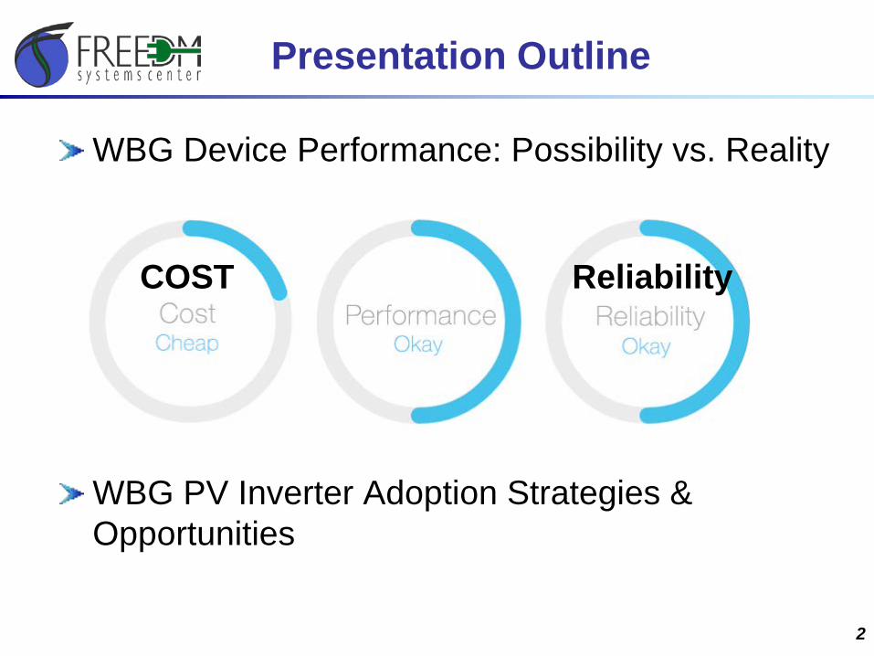
Presentation Outline
WBG Device Performance: Possibility vs. Reality
WBG PV Inverter Adoption Strategies & Opportunities
2
COST Reliability
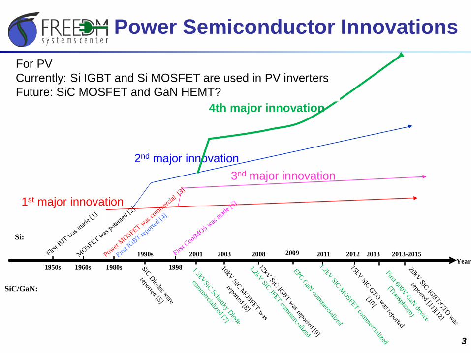
Power Semiconductor Innovations
3
1st major innovation
2nd major innovation3nd major innovation
4th major innovation
First BJT was
made [1]
MOSFET was pate
nted [2
]
SiC Diodes were
reported [5]
1.2kVSiC Schottky Diode
commercialized [7]
Year
SiC/GaN:
Si:
1950s 1960s 1980s
Power MOSFET was
commercial
[3]
First IG
BT reporte
d [4]
1990s
1998
First CoolM
OS was made [
6]
2001 200310kV SiC M
OSFET was
reported [8]
2008
1.2kV SiC JFET commercialized
12kV SiC IGBT was reported [9]
2011
1.2kV SiC MOSFET commercialized
2012
15kV SiC GTO was reported
[10]
2013 2013-2015
20kV SiC IGBT/GTO was
reported [11][12]
2009
EPC GaN commercialized
First 600V GaN device
(Transphorm)Power Semiconductor and PE are everywhereMore Si and WBG devices co-exist for the next 30 yearsFor PVCurrently: Si IGBT and Si MOSFET are used in PV inverters Future: SiC MOSFET and GaN HEMT?
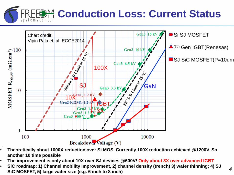
Conduction Loss: Current Status
4
Chart credit: Vipin Pala et. al, ECCE2014
• Theoretically about 1000X reduction over Si MOS. Currently 100X reduction achieved @1200V. So another 10 time possible
• The improvement is only about 10X over SJ devices @600V! Only about 3X over advanced IGBT• SiC roadmap: 1) Channel mobility improvement, 2) channel density (trench) 3) wafer thinning; 4) SJ
SiC MOSFET, 5) large wafer size (e.g. 6 inch to 8 inch)
SJ
10X
GaN
100X
Si SJ MOSFET
7th Gen IGBT(Renesas)
SJ SiC MOSFET(P=10um
IGBT3X
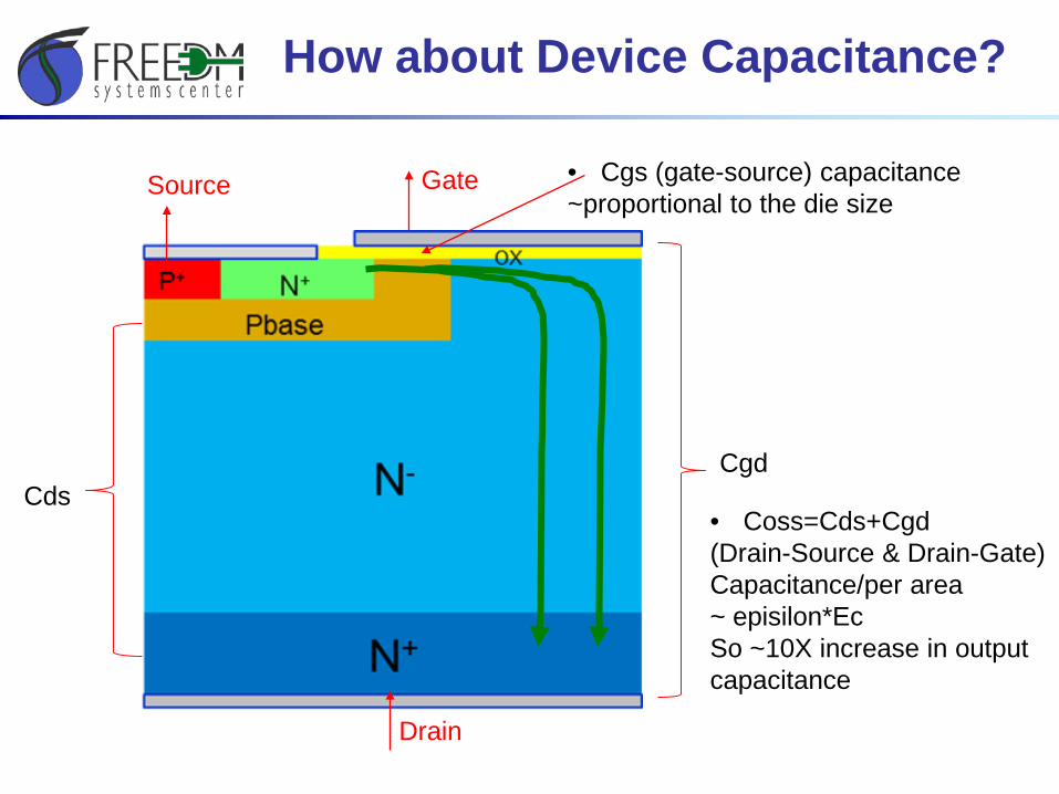
How about Device Capacitance?
• Coss=Cds+Cgd(Drain-Source & Drain-Gate)Capacitance/per area~ episilon*EcSo ~10X increase in outputcapacitance
CdsCgd
Source Gate
Drain
• Cgs (gate-source) capacitance~proportional to the die size
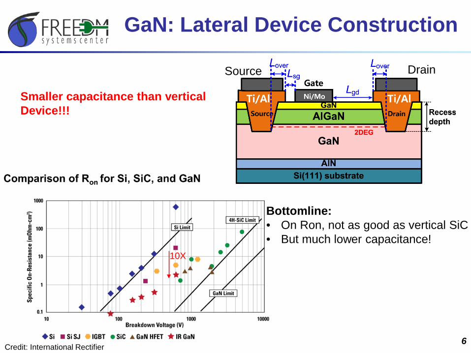
GaN: Lateral Device Construction
6
Bottomline:• On Ron, not as good as vertical SiC• But much lower capacitance!
Credit: International Rectifier
10X
Source Drain
Smaller capacitance than verticalDevice!!!
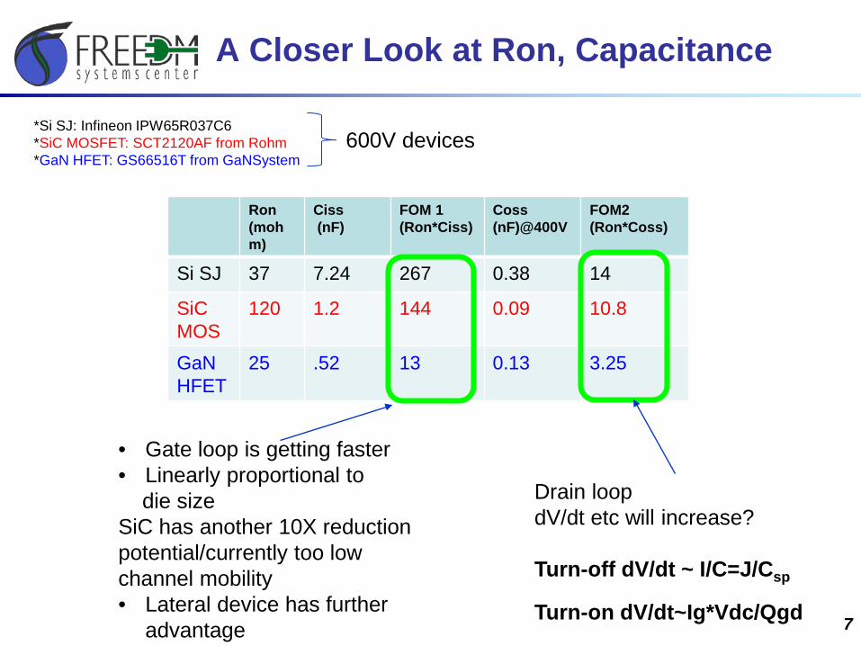
A Closer Look at Ron, Capacitance
7
*Si SJ: Infineon IPW65R037C6*SiC MOSFET: SCT2120AF from Rohm*GaN HFET: GS66516T from GaNSystem
Ron(mohm)
Ciss(nF)
FOM 1 (Ron*Ciss)
Coss(nF)@400V
FOM2(Ron*Coss)
Si SJ 37 7.24 267 0.38 14
SiCMOS
120 1.2 144 0.09 10.8
GaNHFET
25 .52 13 0.13 3.25
• Gate loop is getting faster• Linearly proportional to
die sizeSiC has another 10X reduction potential/currently too low channel mobility• Lateral device has further
advantage
Drain loopdV/dt etc will increase?
Turn-off dV/dt ~ I/C=J/Csp
Turn-on dV/dt~Ig*Vdc/Qgd
600V devices
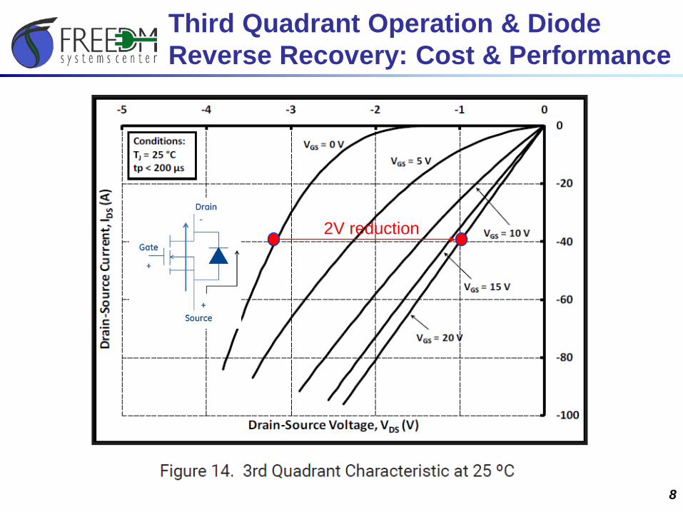
Third Quadrant Operation & Diode Reverse Recovery: Cost & Performance
8
Ron(mohm)
Qrr (uC) FOM (Ron*Qrr)
Si SJ MOS 37 36 1332
Si IGBT 43.7 6.6 288SiC MOS 25 0.406 10GaN HFET 25 0.113 2.8
2V reduction
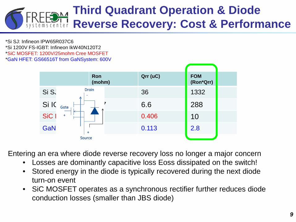
Third Quadrant Operation & Diode Reverse Recovery: Cost & Performance
9
*Si SJ: Infineon IPW65R037C6*Si 1200V FS-IGBT: Infineon IkW40N120T2 *SiC MOSFET: 1200V/25mohm Cree MOSFET*GaN HFET: GS66516T from GaNSystem: 600V
Entering an era where diode reverse recovery loss no longer a major concern• Losses are dominantly capacitive loss Eoss dissipated on the switch!• Stored energy in the diode is typically recovered during the next diode
turn-on event • SiC MOSFET operates as a synchronous rectifier further reduces diode
conduction losses (smaller than JBS diode)
Ron(mohm)
Qrr (uC) FOM (Ron*Qrr)
Si SJ MOS 37 36 1332
Si IGBT 43.7 6.6 288SiC MOS 25 0.406 10GaN HFET 25 0.113 2.8
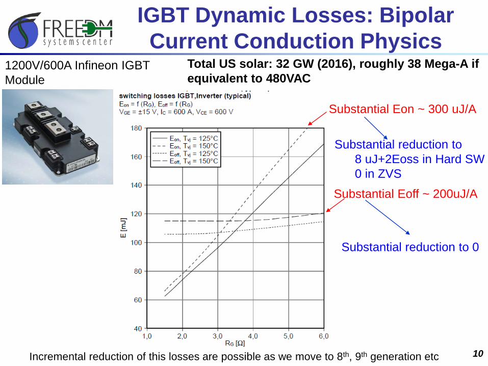
IGBT Dynamic Losses: Bipolar Current Conduction Physics
10
1200V/600A Infineon IGBTModule
Substantial Eon ~ 300 uJ/A
Substantial Eoff ~ 200uJ/A
Incremental reduction of this losses are possible as we move to 8th, 9th generation etc
Substantial reduction to 0
Substantial reduction to8 uJ+2Eoss in Hard SW0 in ZVS
Total US solar: 32 GW (2016), roughly 38 Mega-A if equivalent to 480VAC
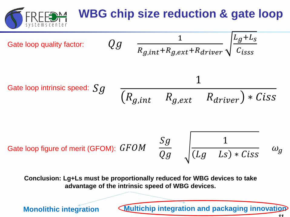
WBG chip size reduction & gate loop
11
𝑄𝑄𝑔𝑔 = 1𝑅𝑅𝑔𝑔,𝑖𝑖𝑖𝑖𝑖𝑖+𝑅𝑅𝑔𝑔,𝑒𝑒𝑒𝑒𝑖𝑖+𝑅𝑅𝑑𝑑𝑑𝑑𝑖𝑖𝑑𝑑𝑒𝑒𝑑𝑑
𝐿𝐿𝑔𝑔+𝐿𝐿𝑠𝑠𝐶𝐶𝑖𝑖𝑠𝑠𝑠𝑠𝑠𝑠
𝑆𝑆𝑔𝑔 =1
𝑅𝑅𝑔𝑔,𝑖𝑖𝑖𝑖𝑖𝑖 + 𝑅𝑅𝑔𝑔,𝑒𝑒𝑒𝑒𝑖𝑖 + 𝑅𝑅𝑑𝑑𝑑𝑑𝑖𝑖𝑑𝑑𝑒𝑒𝑑𝑑 ∗ 𝐶𝐶𝐶𝐶𝐶𝐶𝐶𝐶
𝐺𝐺𝐹𝐹𝐹𝐹𝐹𝐹 =𝑆𝑆𝑔𝑔𝑄𝑄𝑔𝑔
=1
𝐿𝐿𝑔𝑔 + 𝐿𝐿𝐶𝐶 ∗ 𝐶𝐶𝐶𝐶𝐶𝐶𝐶𝐶= 𝜔𝜔𝑔𝑔
Gate loop quality factor:
Gate loop intrinsic speed:
Gate loop figure of merit (GFOM):
Conclusion: Lg+Ls must be proportionally reduced for WBG devices to take advantage of the intrinsic speed of WBG devices.
Monolithic integration Multichip integration and packaging innovation
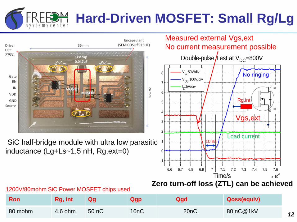
Hard-Driven MOSFET: Small Rg/Lg
12
SiC half-bridge module with ultra low parasitic inductance (Lg+Ls~1.5 nH, Rg,ext=0)
1200V/80mohm SiC Power MOSFET chips used
Ron Rg, int Qg Qgp Qgd Qoss(equiv)
80 mohm 4.6 ohm 50 nC 10nC 20nC 80 nC@1kV
6.6 6.7 6.8 6.9 7 7.1 7.2 7.3 7.4 7.5 7.6
x 10-7
-1
0
1
2
3
4
5
6
7
8
Time/s
Double-pulse Test at VDC=800V
VG:50V/div
VDS:100V/div
ID:5A/div
Measured external Vgs,extNo current measurement possible
Rg,int
Load current
Vgs,ext
10 ns
No ringing
Zero turn-off loss (ZTL) can be achieved
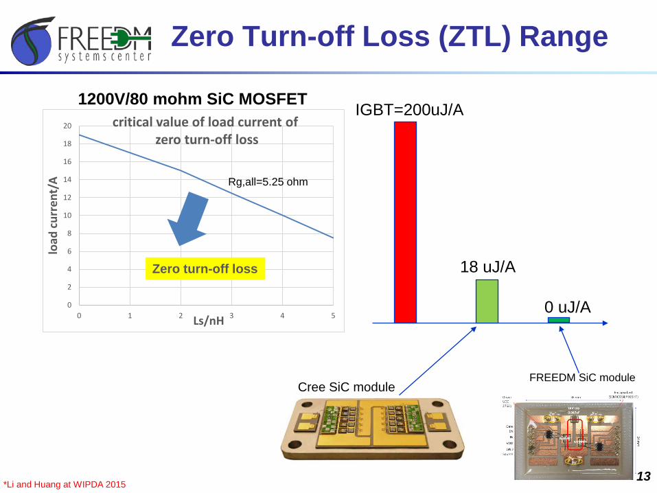
Zero Turn-off Loss (ZTL) Range
13
0
2
4
6
8
10
12
14
16
18
20
0 1 2 3 4 5
load
cur
rent
/A
Ls/nH
critical value of load current of zero turn-off loss
Zero turn-off loss
Rg,all=5.25 ohm
*Li and Huang at WIPDA 2015
IGBT=200uJ/A
18 uJ/A
0 uJ/A
Cree SiC moduleFREEDM SiC module
1200V/80 mohm SiC MOSFET
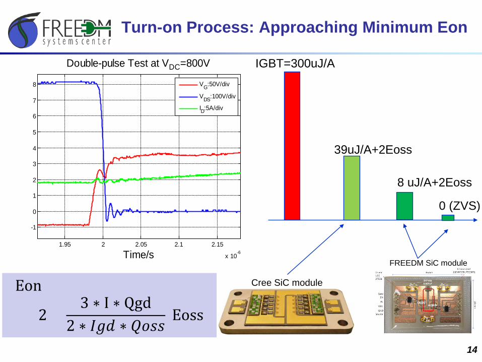
Turn-on Process: Approaching Minimum Eon
14
1.95 2 2.05 2.1 2.15
x 10-6
-1
0
1
2
3
4
5
6
7
8
Time/s
Double-pulse Test at VDC=800V
VG:50V/div
VDS:100V/div
ID:5A/div
IGBT=300uJ/A
Cree SiC module
39uJ/A+2Eoss
FREEDM SiC module
Eon
= (2 +3 ∗ I ∗ Qgd
2 ∗ 𝐼𝐼𝑔𝑔𝐼𝐼 ∗ 𝑄𝑄𝑄𝑄𝐶𝐶𝐶𝐶)Eoss
8 uJ/A+2Eoss
0 (ZVS)
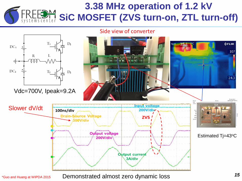
3.38 MHz operation of 1.2 kV SiC MOSFET (ZVS turn-on, ZTL turn-off)
15
100ns/div
ZVS
Demonstrated almost zero dynamic loss*Guo and Huang at WIPDA 2015
Estimated Tj=43oC
Slower dV/dt
Vdc=700V, Ipeak=9.2A
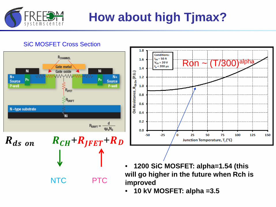
How about high Tjmax?
SiC MOSFET Cross Section
NTC PTC
Ron ~ (T/300)alpha
𝑹𝑹𝒅𝒅𝒅𝒅(𝒐𝒐𝒐𝒐) = 𝑹𝑹𝑪𝑪𝑪𝑪+𝑹𝑹𝑱𝑱𝑱𝑱𝑱𝑱𝑱𝑱+𝑹𝑹𝑫𝑫
• 1200 SiC MOSFET: alpha=1.54 (this will go higher in the future when Rch is improved• 10 kV MOSFET: alpha =3.5
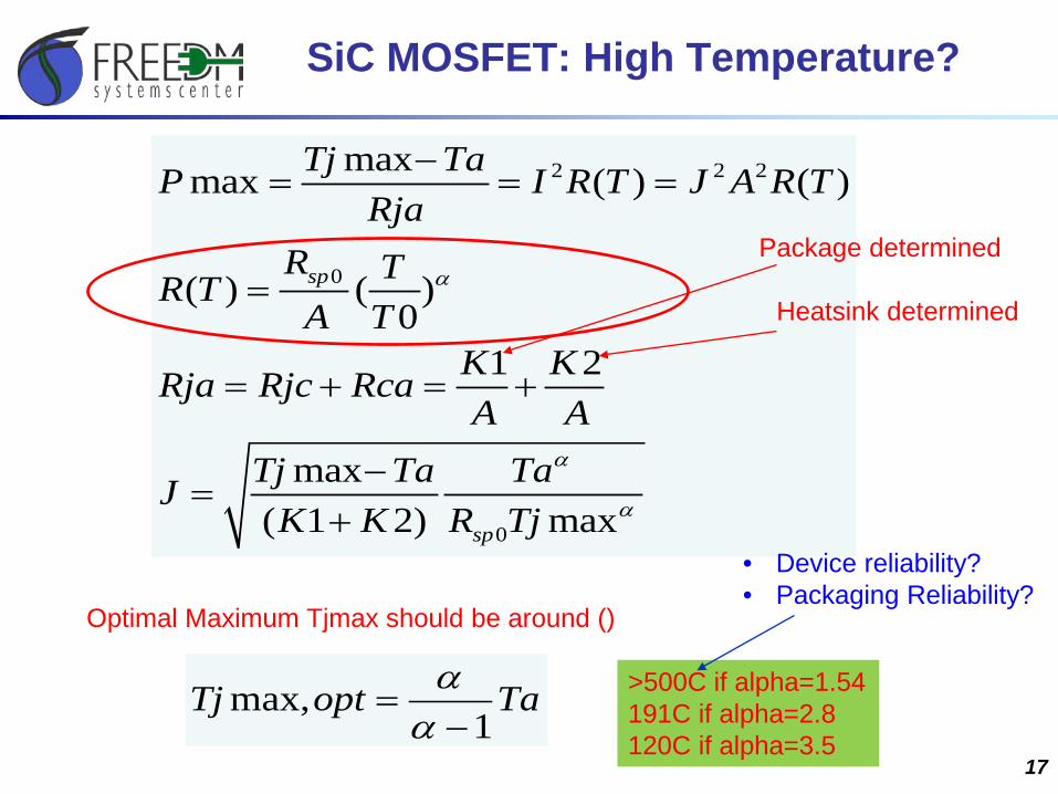
SiC MOSFET: High Temperature?
17
2 2 2
0
0
maxmax ( ) ( )
( ) ( )0
1 2
max( 1 2) max
sp
sp
Tj TaP I R T J A R TRja
R TR TA T
K KRja Rjc RcaA A
Tj Ta TaJK K R Tj
α
α
α
−= = =
=
= + = +
−=
+
Optimal Maximum Tjmax should be around ()
TaoptTj1
max,−
=αα >500C if alpha=1.54
191C if alpha=2.8120C if alpha=3.5
Package determined
Heatsink determined
• Device reliability?• Packaging Reliability?
18
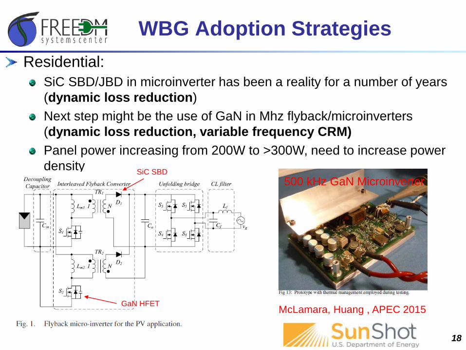
WBG Adoption Strategies
500 kHz GaN Microinverter
McLamara, Huang , APEC 2015
Residential: SiC SBD/JBD in microinverter has been a reality for a number of years (dynamic loss reduction)Next step might be the use of GaN in Mhz flyback/microinverters(dynamic loss reduction, variable frequency CRM)Panel power increasing from 200W to >300W, need to increase power density SiC SBD
GaN HFET
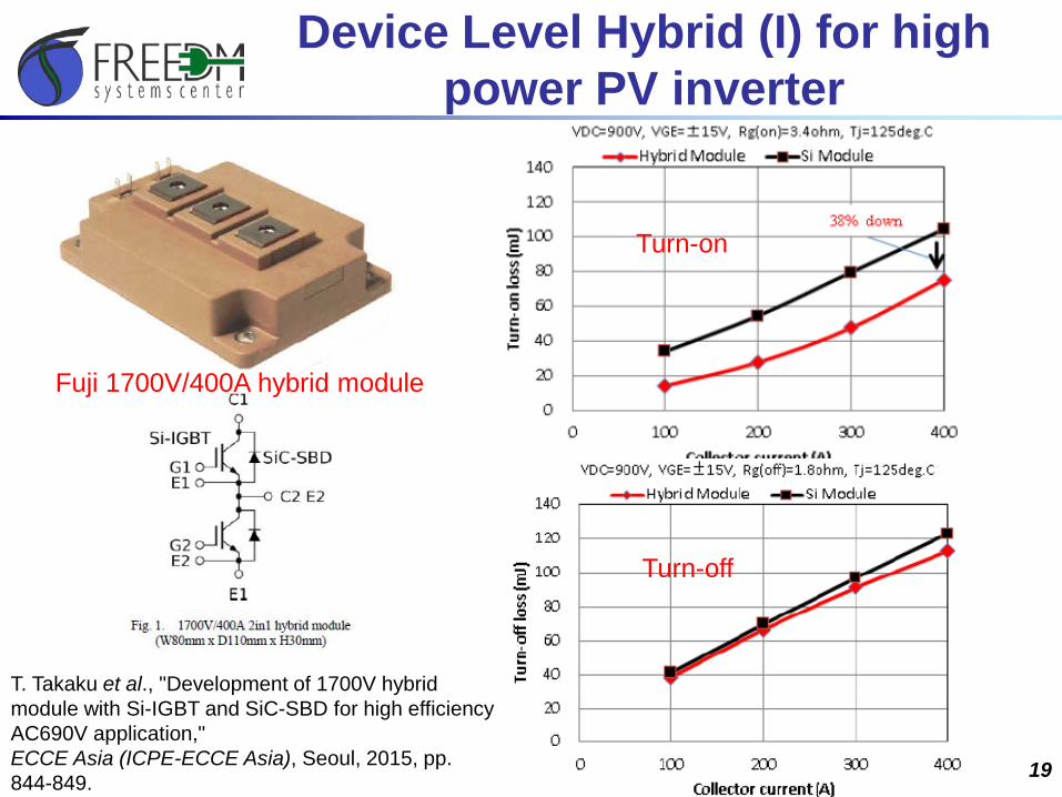
Device Level Hybrid (I) for high power PV inverter
19
Turn-on
Turn-off
T. Takaku et al., "Development of 1700V hybrid module with Si-IGBT and SiC-SBD for high efficiency AC690V application,"ECCE Asia (ICPE-ECCE Asia), Seoul, 2015, pp. 844-849.
Fuji 1700V/400A hybrid module
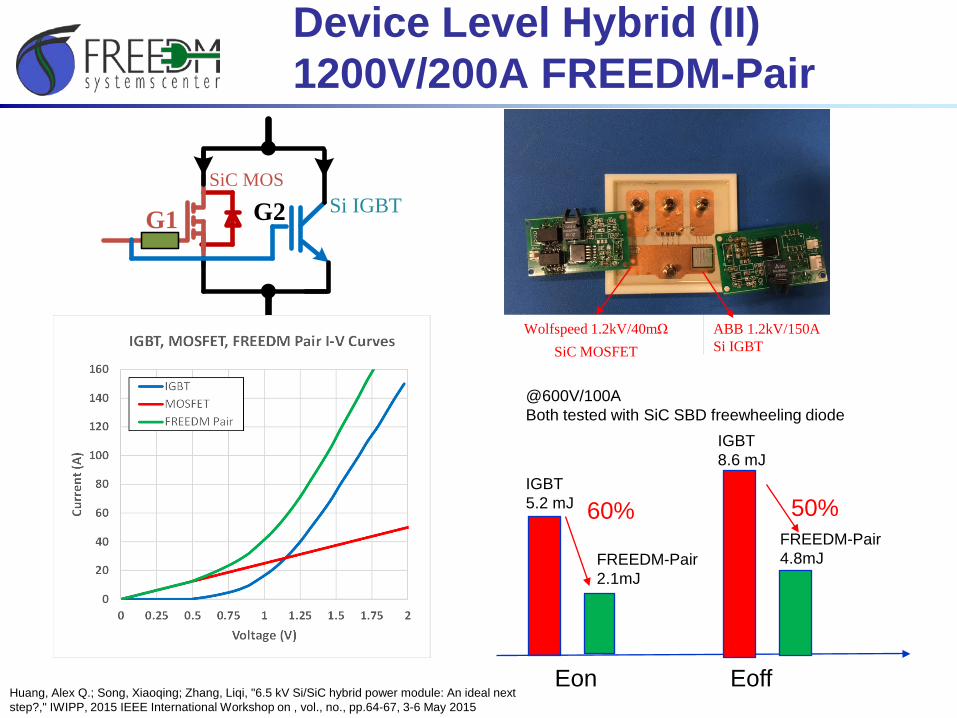
Device Level Hybrid (II) 1200V/200A FREEDM-Pair
Wolfspeed 1.2kV/40mΩSiC MOSFET
ABB 1.2kV/150A Si IGBT
G1 G2SiC MOS
Si IGBT
(a)
Huang, Alex Q.; Song, Xiaoqing; Zhang, Liqi, "6.5 kV Si/SiC hybrid power module: An ideal next step?," IWIPP, 2015 IEEE International Workshop on , vol., no., pp.64-67, 3-6 May 2015
IGBT5.2 mJ
FREEDM-Pair2.1mJ
@600V/100ABoth tested with SiC SBD freewheeling diode
Eon Eoff
IGBT8.6 mJ
FREEDM-Pair4.8mJ
50%60%
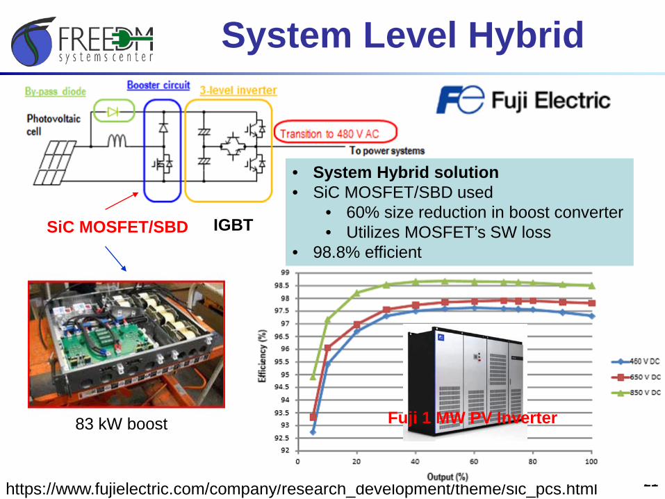
System Level Hybrid
21
IGBTSiC MOSFET/SBD
https://www.fujielectric.com/company/research_development/theme/sic_pcs.html
• System Hybrid solution• SiC MOSFET/SBD used
• 60% size reduction in boost converter• Utilizes MOSFET’s SW loss
• 98.8% efficient
Fuji 1 MW PV Inverter83 kW boost
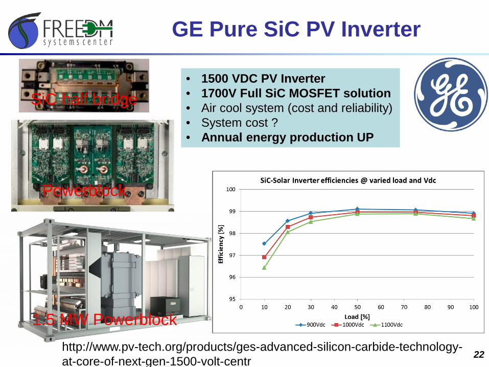
GE Pure SiC PV Inverter
22
• 1500 VDC PV Inverter• 1700V Full SiC MOSFET solution• Air cool system (cost and reliability)• System cost ?• Annual energy production UP
Powerblock
1.5 MW Powerblock
SiC half bridge
http://www.pv-tech.org/products/ges-advanced-silicon-carbide-technology-at-core-of-next-gen-1500-volt-centr
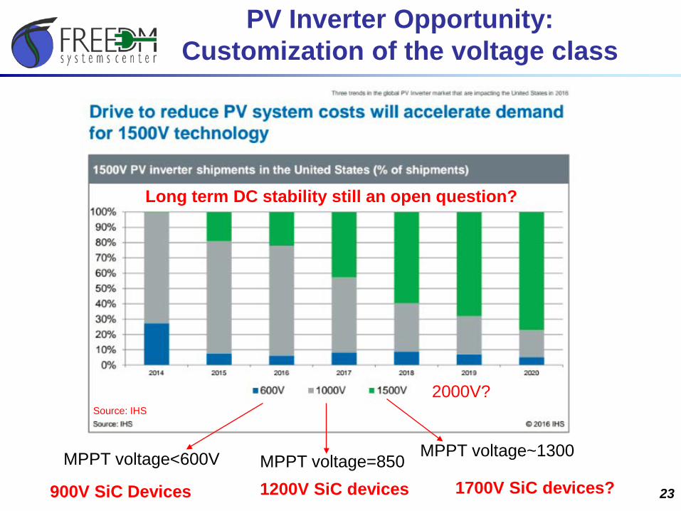
PV Inverter Opportunity: Customization of the voltage class
23900V SiC Devices 1200V SiC devices 1700V SiC devices?MPPT voltage<600V MPPT voltage=850 MPPT voltage~1300
Source: IHS
2000V?
Long term DC stability still an open question?
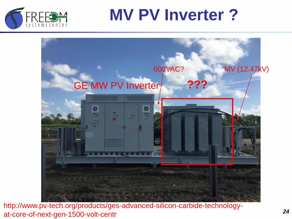
MV PV Inverter ?
24
GE MW PV Inverter ???600VAC? MV (12.47kV)
http://www.pv-tech.org/products/ges-advanced-silicon-carbide-technology-at-core-of-next-gen-1500-volt-centr
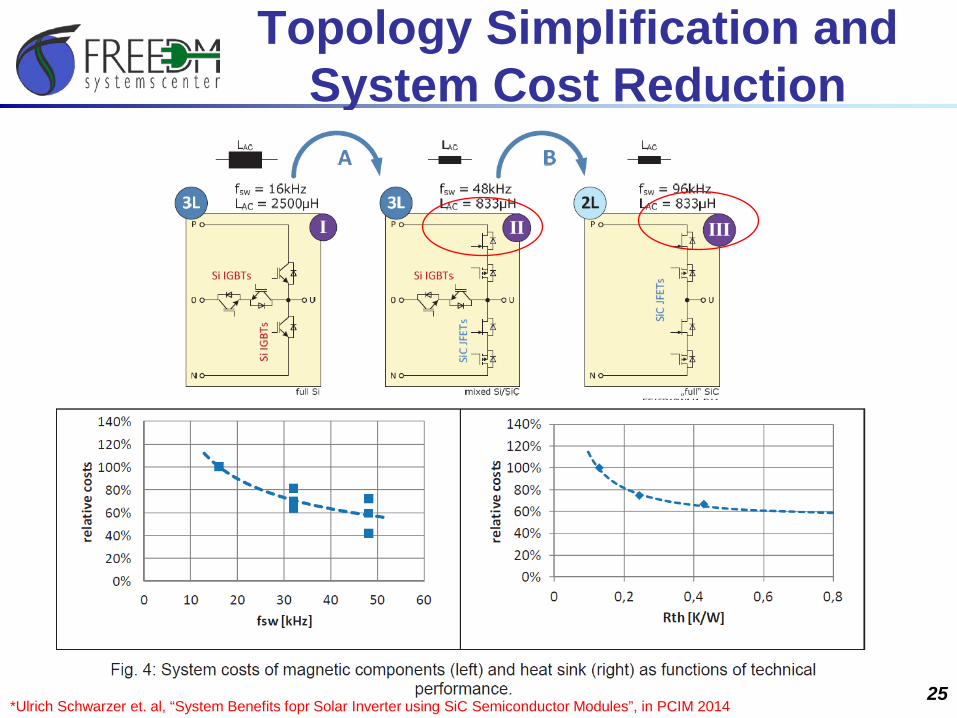
Topology Simplification and System Cost Reduction
25*Ulrich Schwarzer et. al, “System Benefits fopr Solar Inverter using SiC Semiconductor Modules”, in PCIM 2014
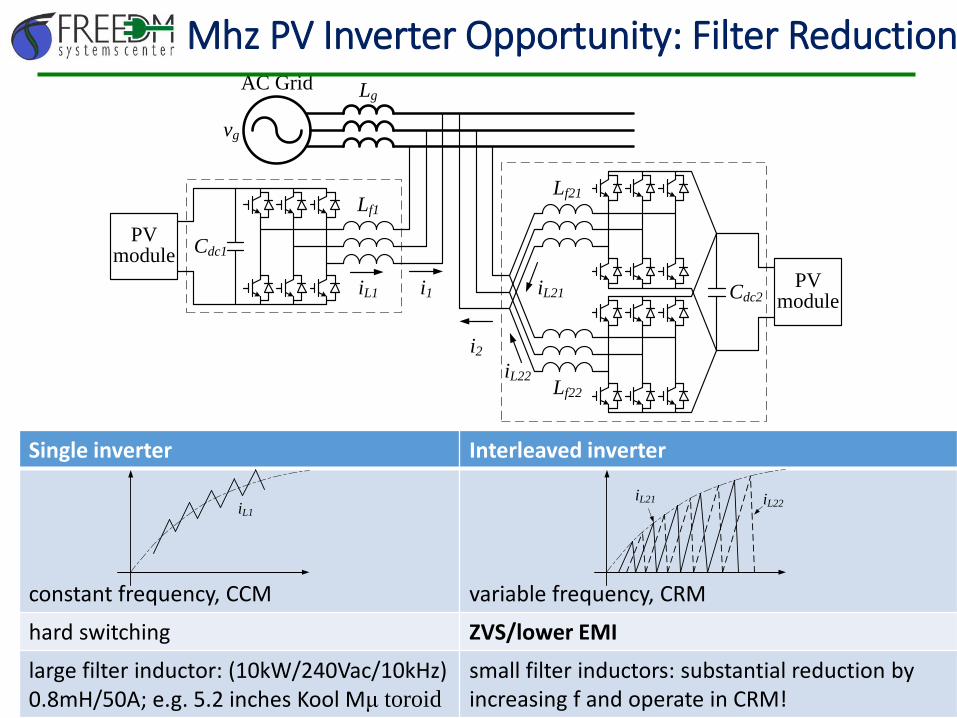
vg
LgAC Grid
Lf1
Cdc1PV
module
Lf21
iL21 Cdc2PV
modulei1
i2
iL1
Lf22iL22
Single inverter Interleaved inverter
constant frequency, CCM variable frequency, CRM
hard switching ZVS/lower EMI
large filter inductor: (10kW/240Vac/10kHz)0.8mH/50A; e.g. 5.2 inches Kool Mμ toroid
small filter inductors: substantial reduction by increasing f and operate in CRM!
iL1iL21 iL22
Mhz PV Inverter Opportunity: Filter Reduction
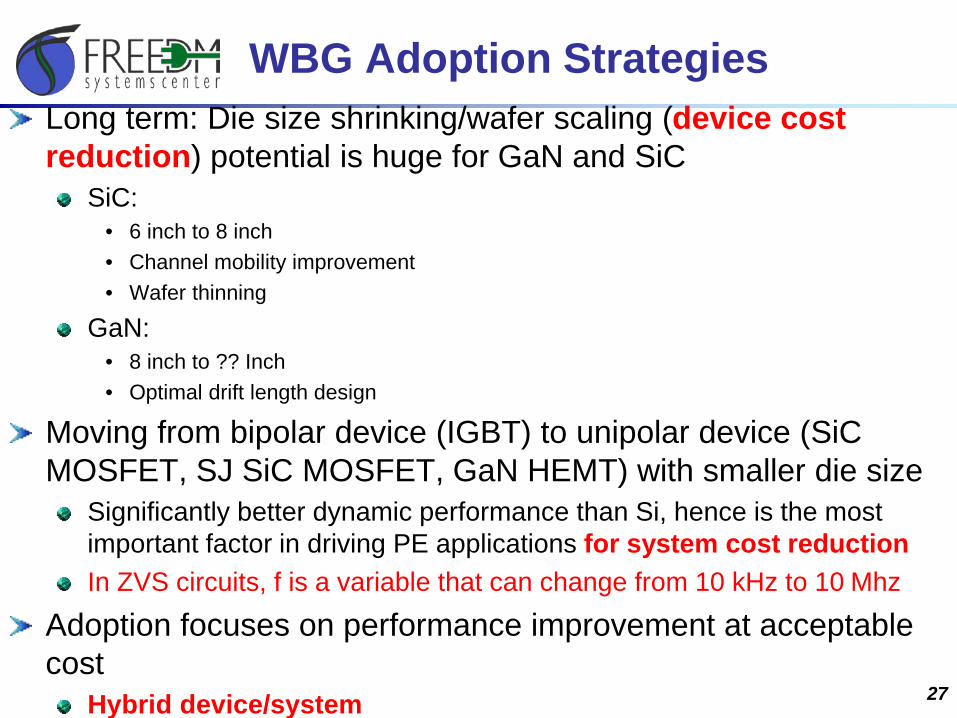
Long term: Die size shrinking/wafer scaling (device cost reduction) potential is huge for GaN and SiC
SiC: • 6 inch to 8 inch• Channel mobility improvement• Wafer thinning
GaN: • 8 inch to ?? Inch• Optimal drift length design
Moving from bipolar device (IGBT) to unipolar device (SiCMOSFET, SJ SiC MOSFET, GaN HEMT) with smaller die size
Significantly better dynamic performance than Si, hence is the most important factor in driving PE applications for system cost reductionIn ZVS circuits, f is a variable that can change from 10 kHz to 10 Mhz
Adoption focuses on performance improvement at acceptable cost
Hybrid device/system 27
WBG Adoption Strategies

Thank You
28