Embed Size (px)
Citation preview
WARP: HardwareCharles Camp
WARP WorkshopIndian Institute of Technology
November 30, 2007
warp.rice.edu
WARP Hardware
• WARP Board-Level Components
- FPGA Board
- Radio Board
- Clock Board
• WARP FPGA Device Architecture
• WARP Design Flows
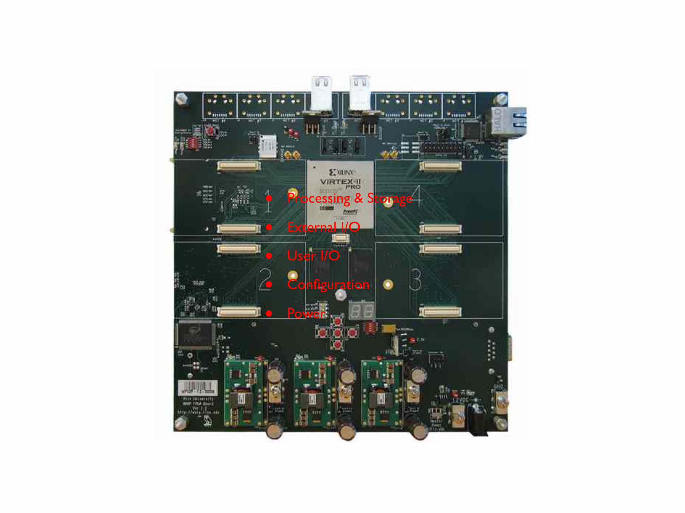
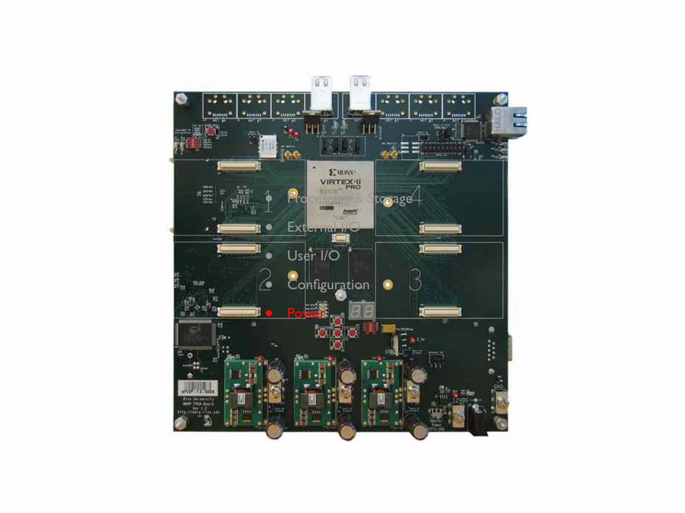
• Processing & Storage
• External I/O
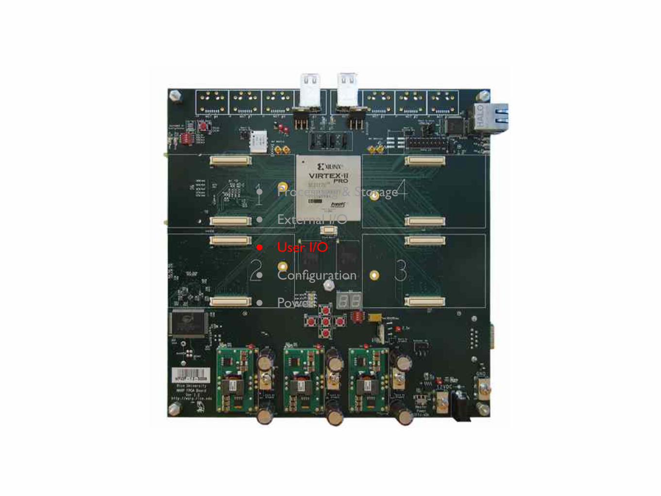
• User I/O
• Configuration
• Power
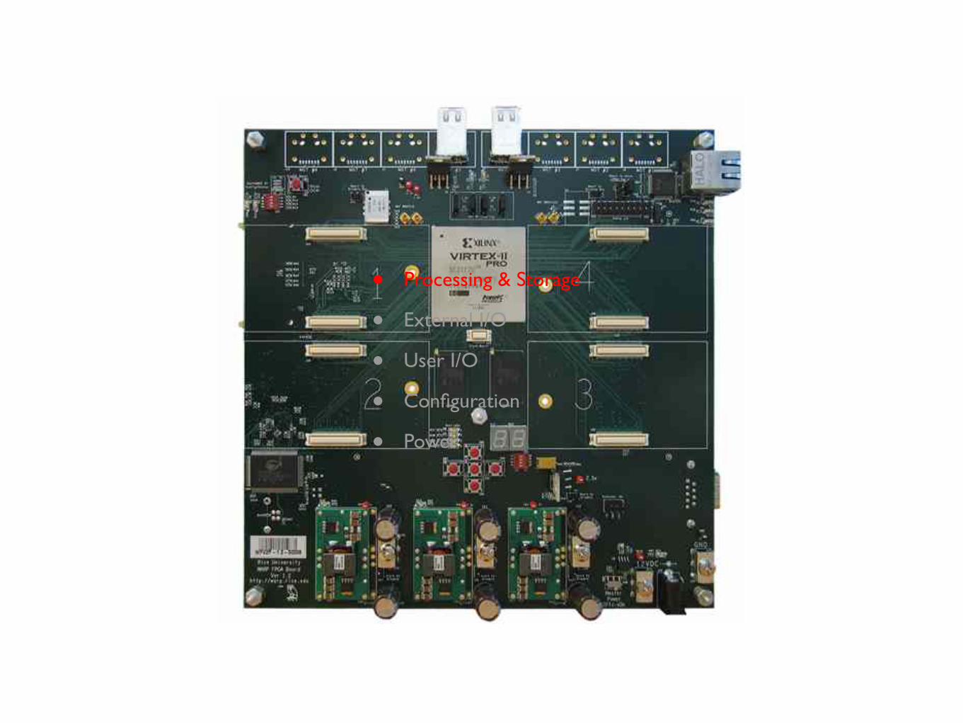
• Processing & Storage
• External I/O
• User I/O
• Configuration
• Power
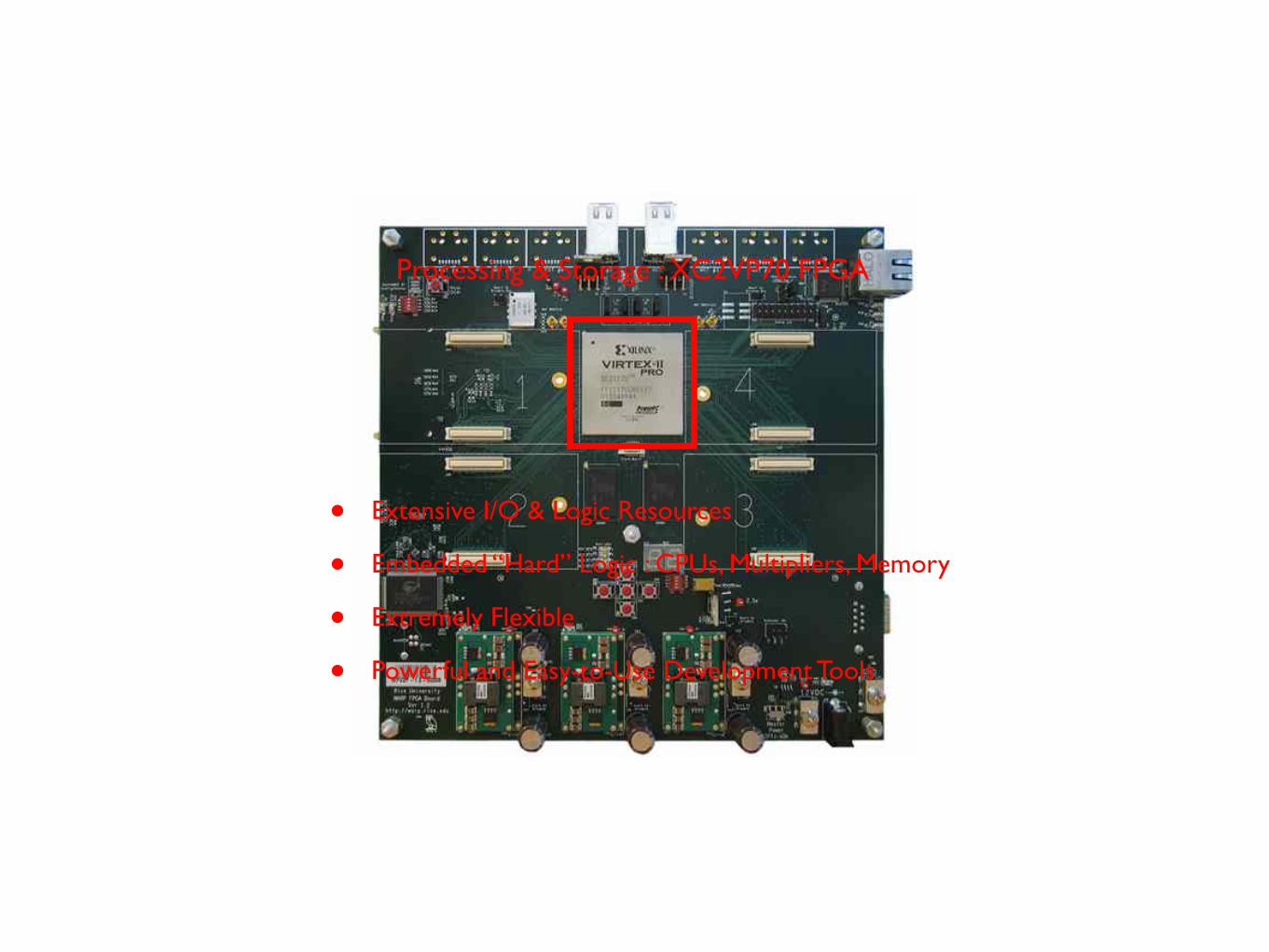
• Extensive I/O & Logic Resources
• Embedded “Hard” Logic : CPUs, Multipliers, Memory
• Extremely Flexible
• Powerful and Easy-to-Use Development Tools
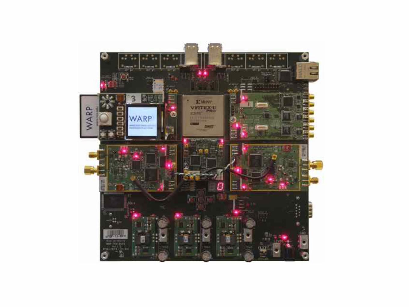
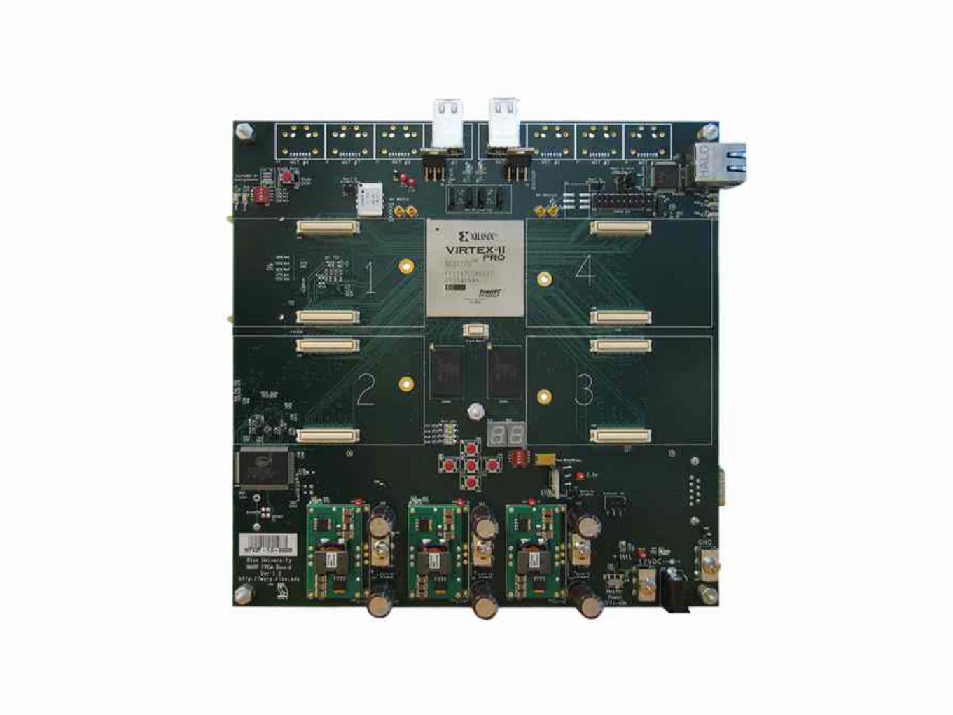
Processing & Storage : XC2VP70 FPGA

• Augments FPGA’s Internal RAM Resources
• Usable as Instruction and/or Data Memory
• Two ICs, Each 512K x 32
Processing & Storage : 4 MByte Onboard SRAM

• Processing & Storage
• External I/O
• User I/O
• Configuration
• Power
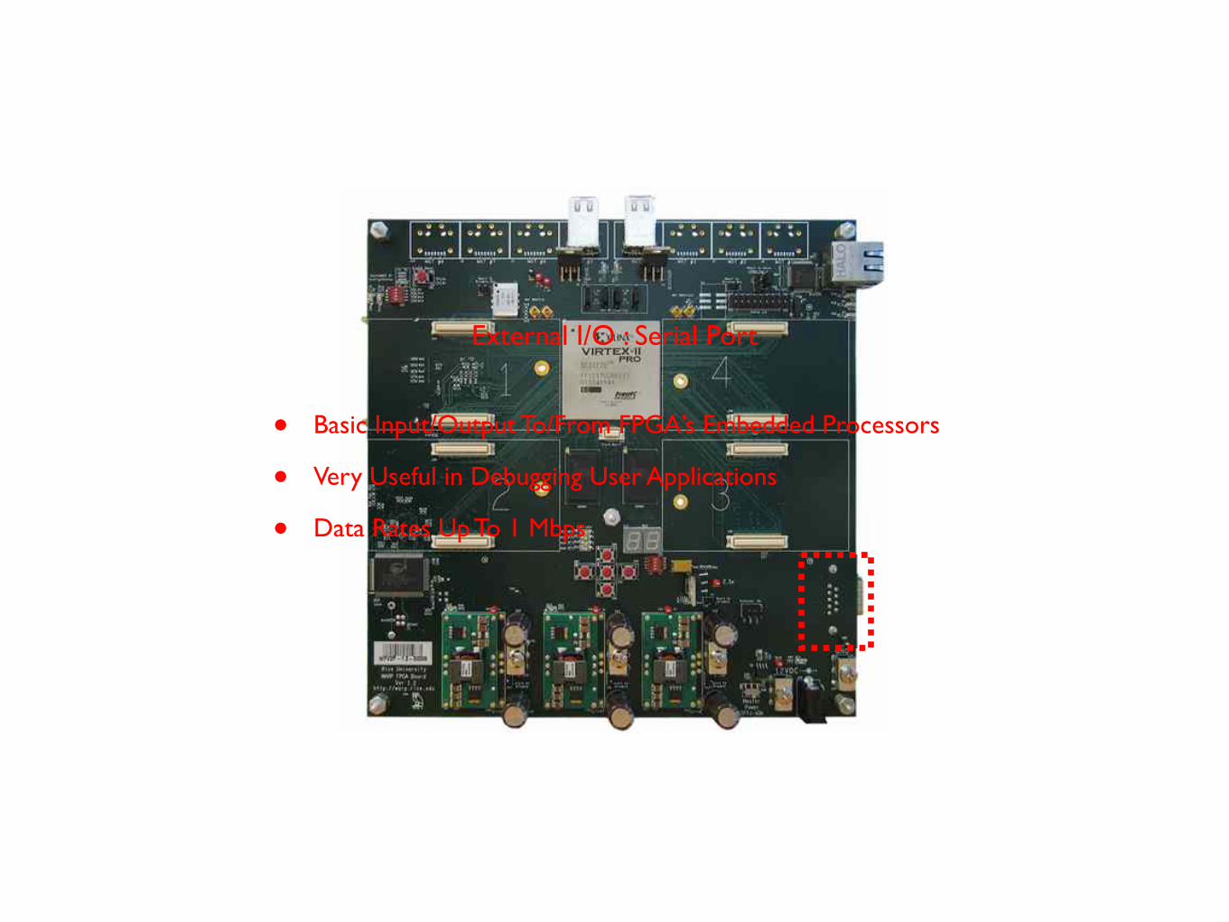
• Basic Input/Output To/From FPGA’s Embedded Processors
• Very Useful in Debugging User Applications
• Data Rates Up To 1 Mbps
External I/O : Serial Port
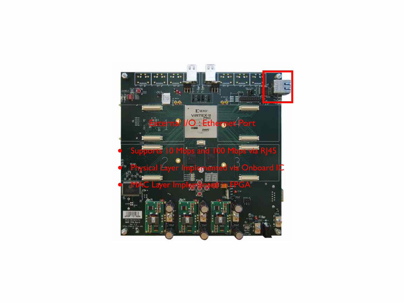
• Supports 10 Mbps and 100 Mbps via RJ45
• Physical Layer Implemented via Onboard IC
• MAC Layer Implemented in FPGA
External I/O : Ethernet Port
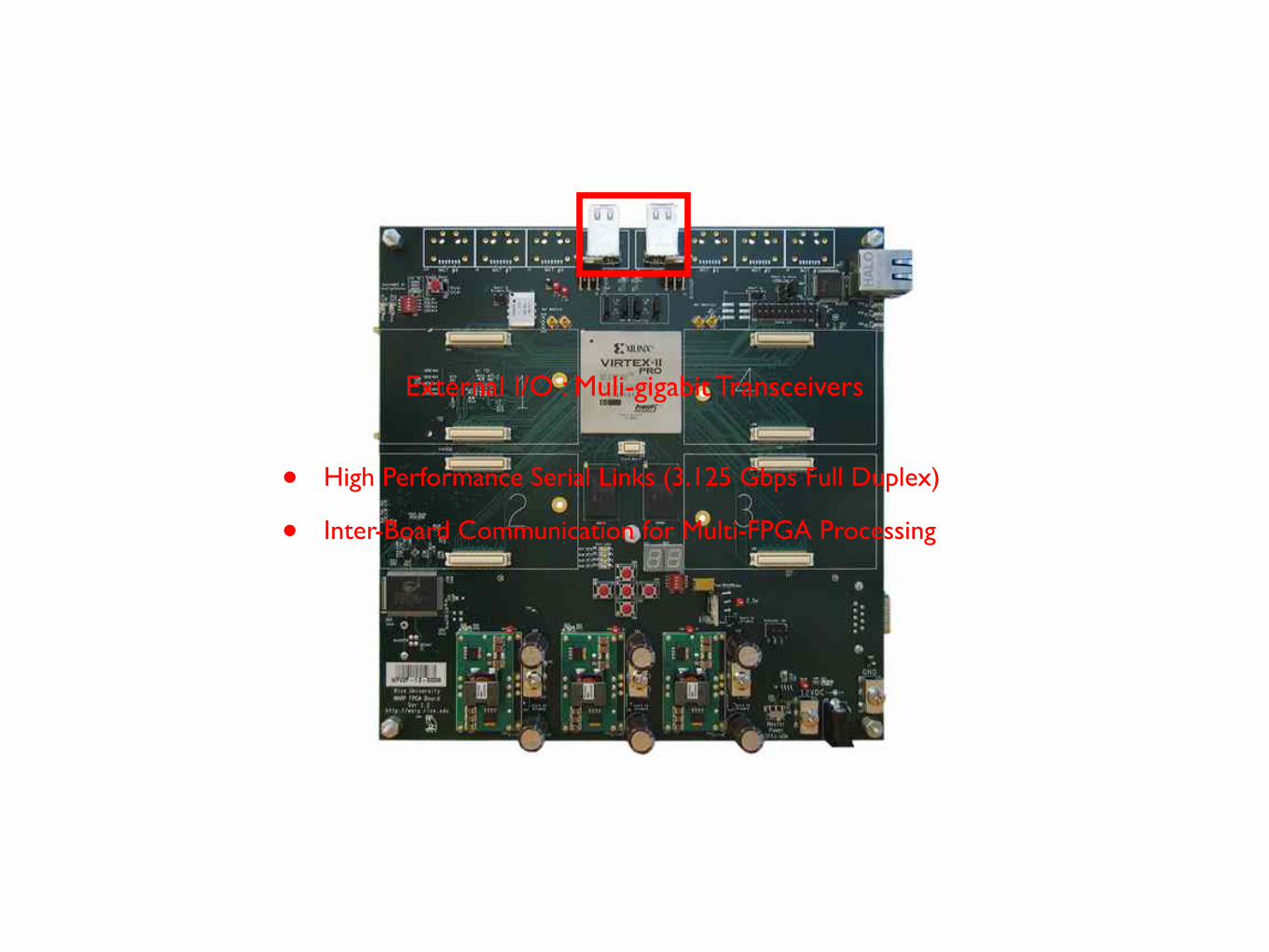
• High Performance Serial Links (3.125 Gbps Full Duplex)
• Inter-Board Communication for Multi-FPGA Processing
External I/O : Muli-gigabit Transceivers
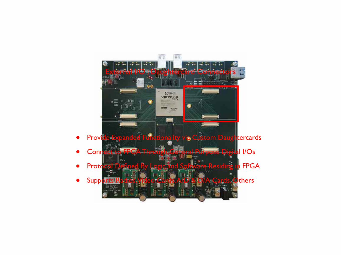
External I/O : Daughtercard Connectors
• Provide Expanded Functionality via Custom Daughtercards
• Connect to FPGA Through General Purpose Digital I/Os
• Protocol Defined By Logic and Software Residing in FPGA
• Supports Radios, Video Cards, A/D & D/A Cards, Others
• Processing & Storage
• External I/O
• User I/O
• Configuration
• Power
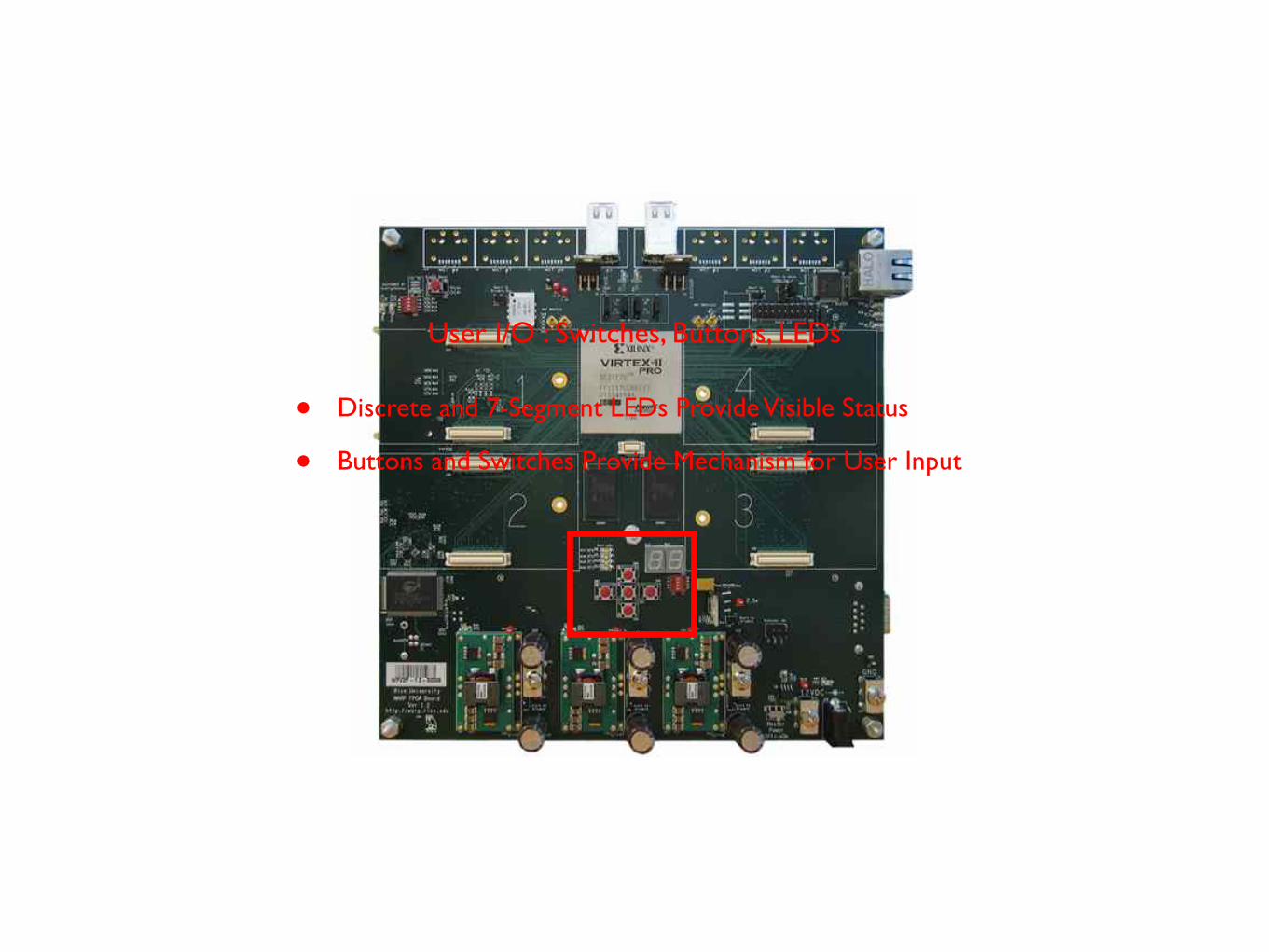
User I/O : Switches, Buttons, LEDs
• Discrete and 7-Segment LEDs Provide Visible Status
• Buttons and Switches Provide Mechanism for User Input
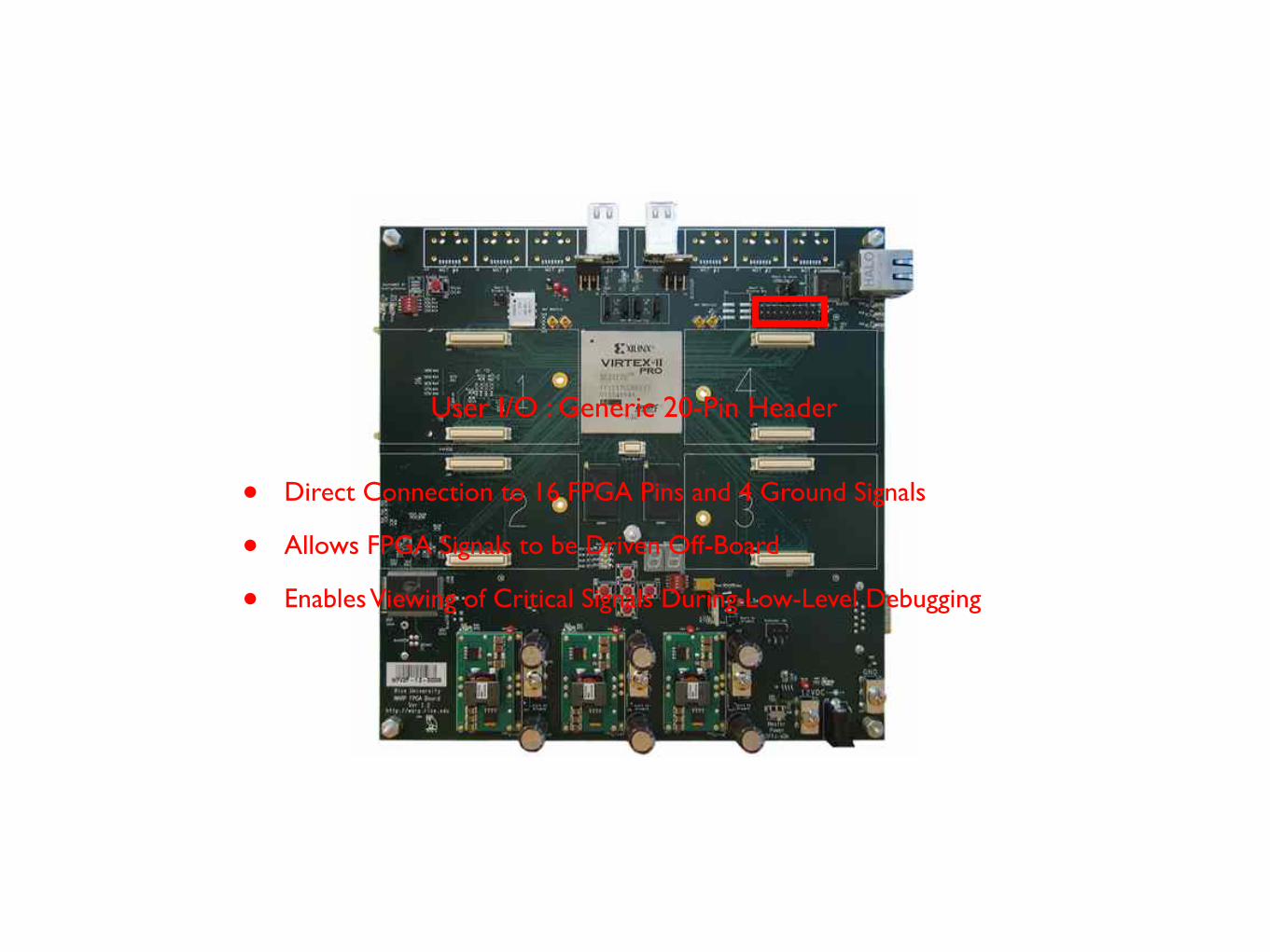
User I/O : Generic 20-Pin Header
• Direct Connection to 16 FPGA Pins and 4 Ground Signals
• Allows FPGA Signals to be Driven Off-Board
• Enables Viewing of Critical Signals During Low-Level Debugging

• Processing & Storage
• External I/O
• User I/O
• Configuration
• Power

Configuration : Compact Flash Slot
• Configures FPGA From File(s) Stored on CF Card
• Multiple Programs Selectable via Switches on PCB
• Accessible by FPGA for Non-Volatile Storage
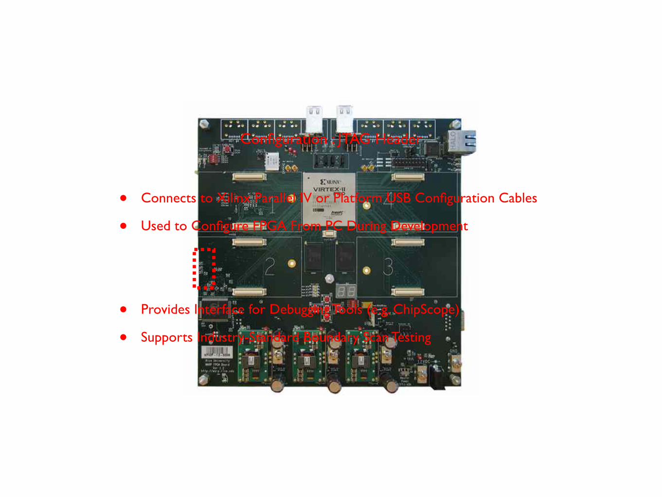
• Connects to Xilinx Parallel IV or Platform USB Configuration Cables
• Used to Configure FPGA From PC During Development
• Provides Interface for Debugging Tools (e.g. ChipScope)
• Supports Industry-Standard Boundary Scan Testing
Configuration : JTAG Header
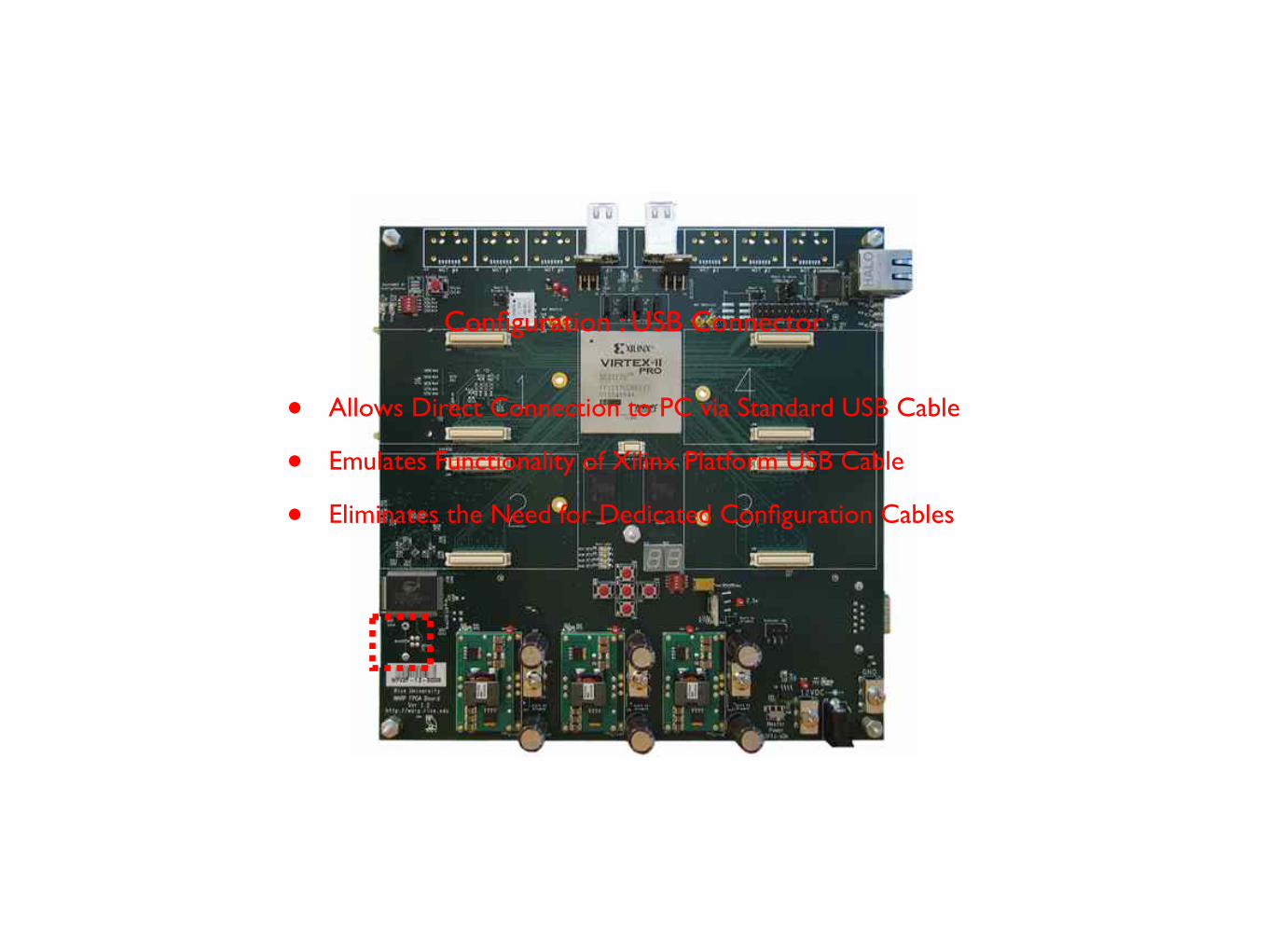
Configuration : USB Connector
• Allows Direct Connection to PC via Standard USB Cable
• Emulates Functionality of Xilinx Platform USB Cable
• Eliminates the Need for Dedicated Configuration Cables
• Processing & Storage
• External I/O
• User I/O
• Configuration
• Power
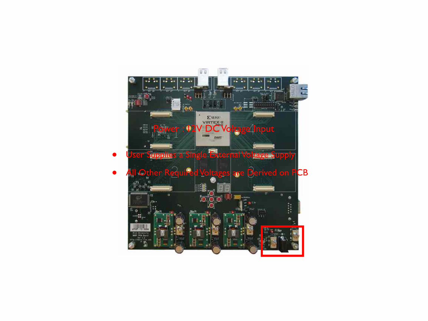
Power : 12V DC Voltage Input
• User Supplies a Single External Voltage Supply
• All Other Required Voltages are Derived on PCB
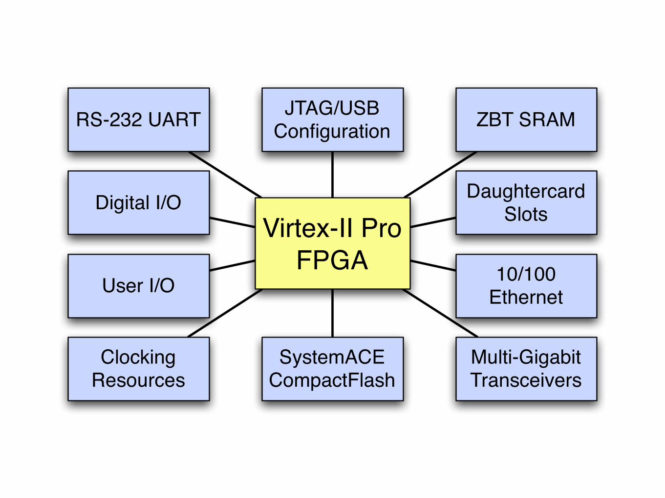
Virtex-II Pro
FPGA
Daughtercard Slots
ZBT SRAM
10/100 Ethernet
RS-232 UART
Digital I/O
User I/O
Multi-Gigabit Transceivers
Clocking Resources
SystemACECompactFlash
JTAG/USB Configuration
Questions?
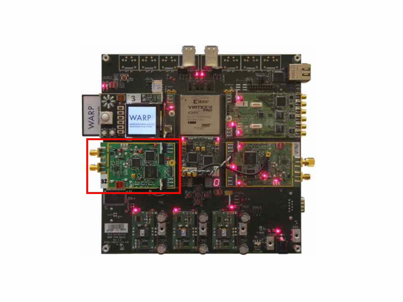
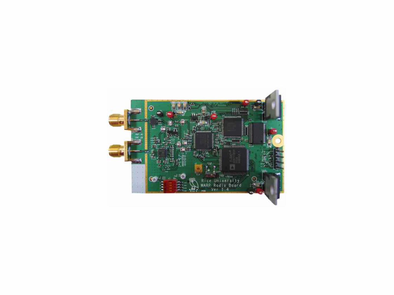
WARP Hardware
• WARP Board-Level Components
- FPGA Board
- Radio Board
- Clock Board
• WARP FPGA Device Architecture
• WARP Design Flows
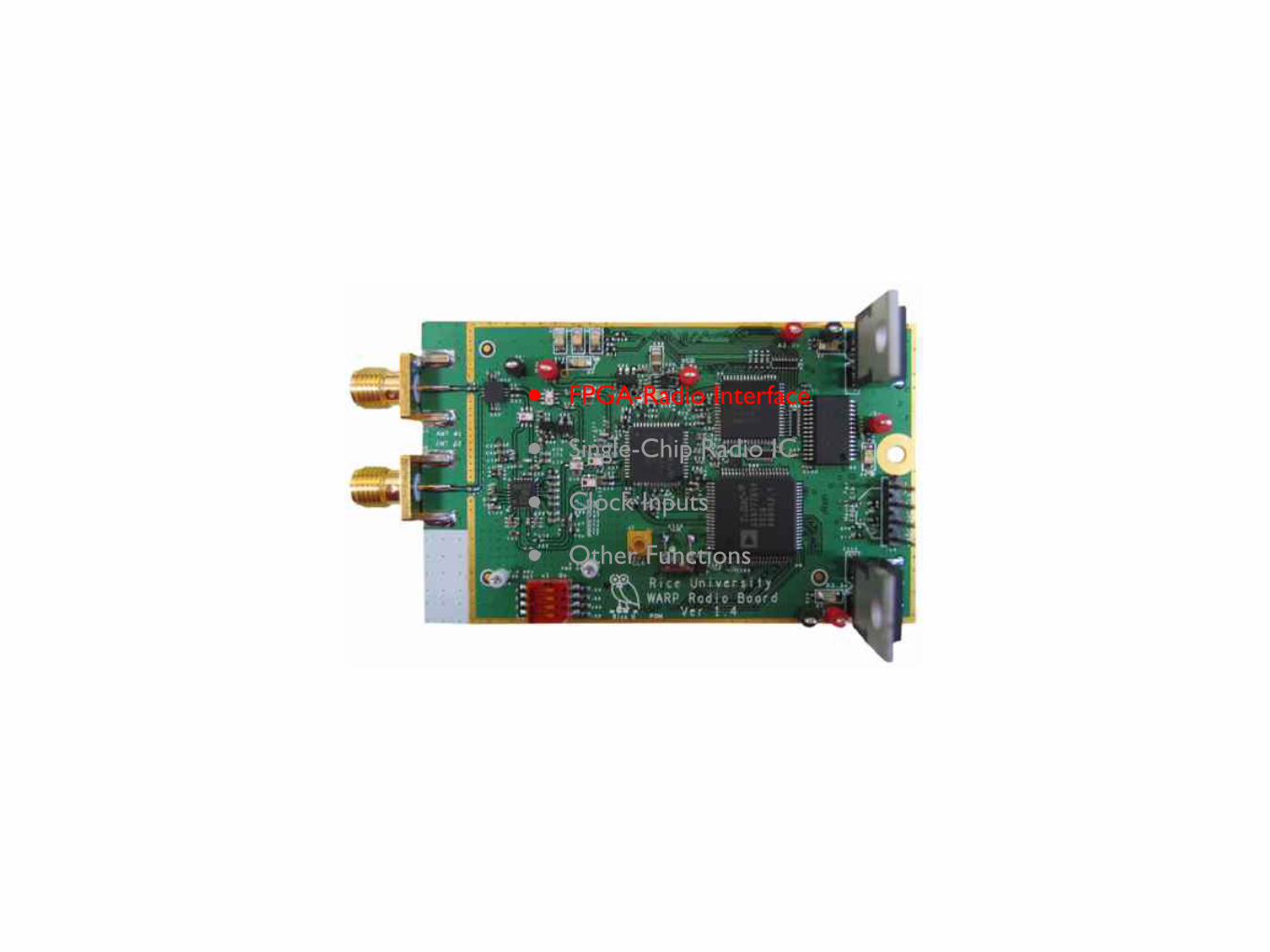
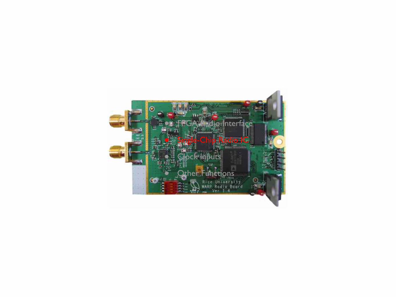
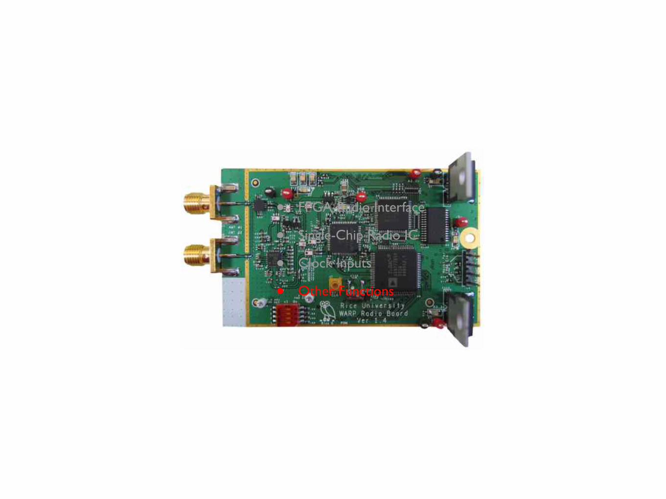
• FPGA-Radio Interface
• Single-Chip Radio IC
• Clock Inputs
• Other Functions
• FPGA-Radio Interface
• Single-Chip Radio IC
• Clock Inputs
• Other Functions
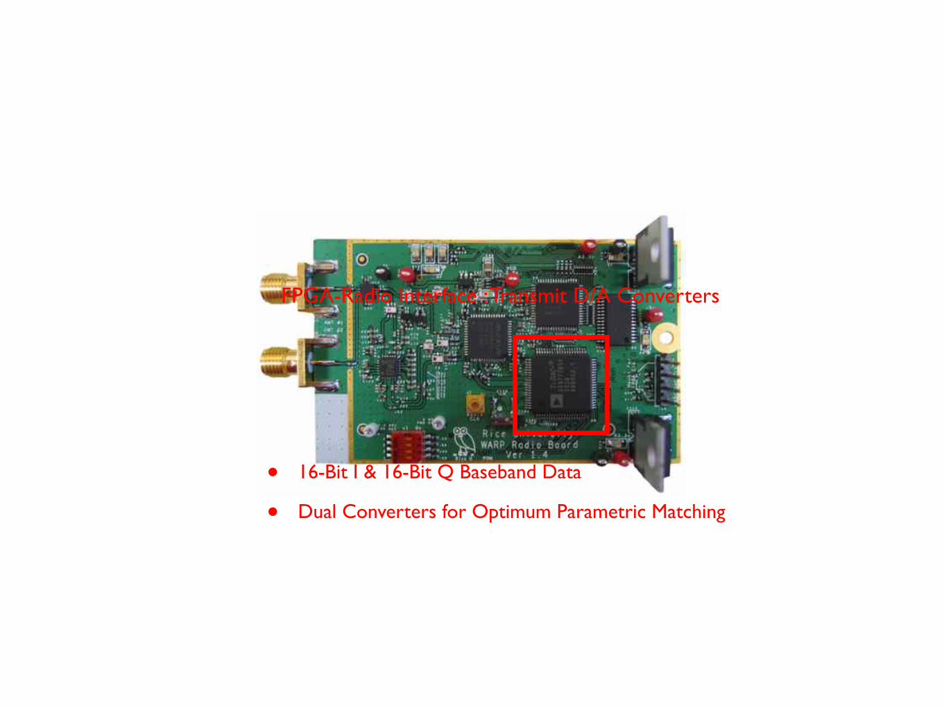
FPGA-Radio Interface : Transmit D/A Converters
• 16-Bit I & 16-Bit Q Baseband Data
• Dual Converters for Optimum Parametric Matching
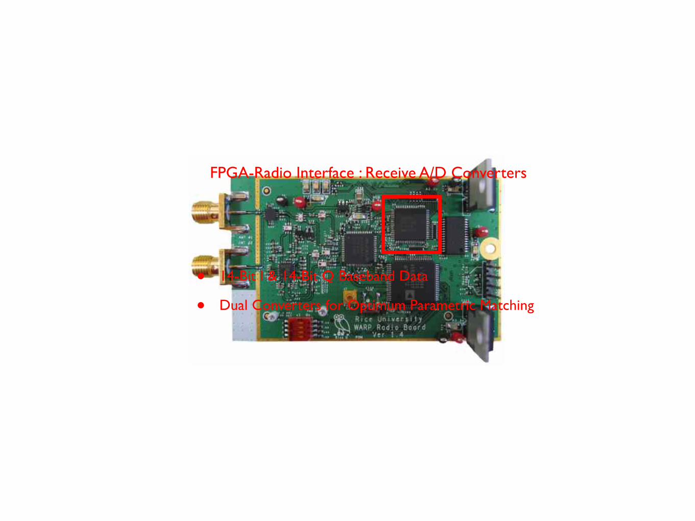
FPGA-Radio Interface : Receive A/D Converters
• 14-Bit I & 14-Bit Q Baseband Data
• Dual Converters for Optimum Parametric Matching
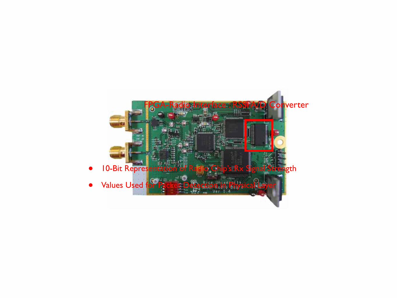
FPGA-Radio Interface : RSSI A/D Converter
• 10-Bit Representation of Radio Chip’s Rx Signal Strength
• Values Used for Packet Detection in Physical Layer
• FPGA-Radio Interface
• Single-Chip Radio IC
• Clock Inputs
• Other Functions
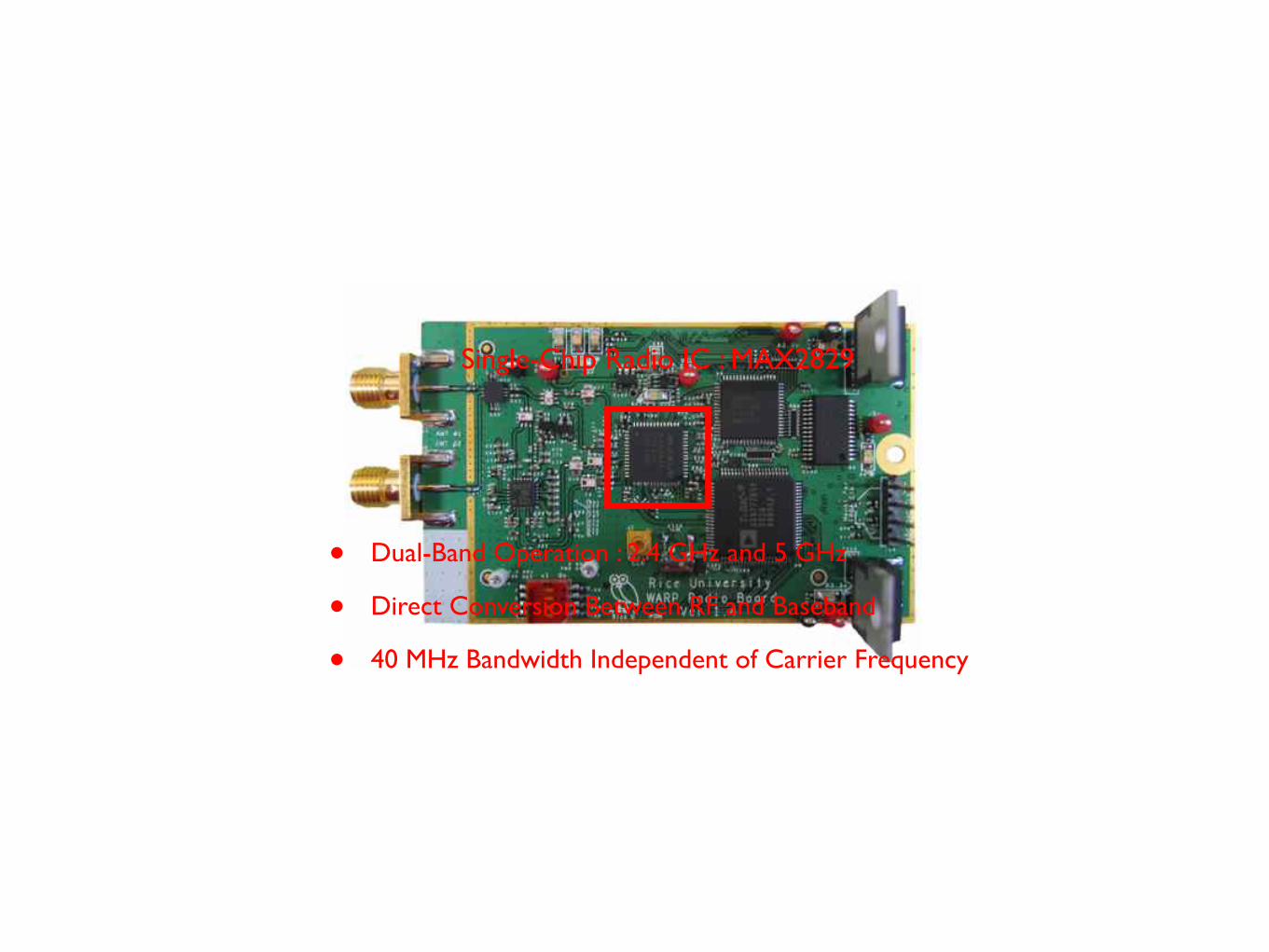
Single-Chip Radio IC : MAX2829
• Dual-Band Operation : 2.4 GHz and 5 GHz
• Direct Conversion Between RF and Baseband
• 40 MHz Bandwidth Independent of Carrier Frequency

• FPGA-Radio Interface
• Single-Chip Radio IC
• Clock Inputs
• Other Functions
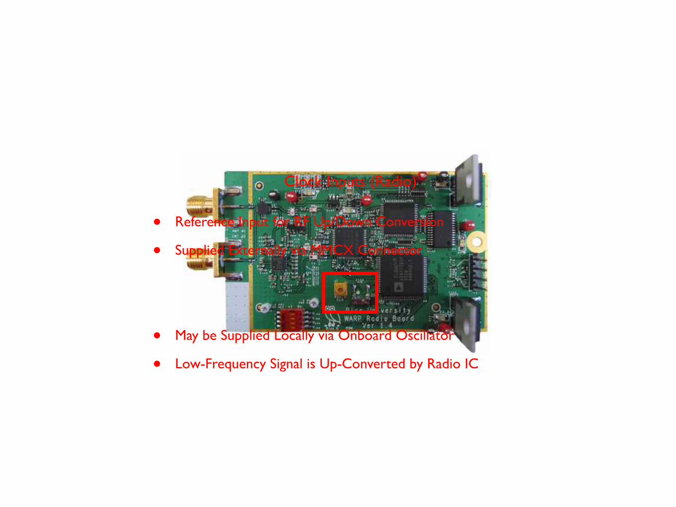
Clock Inputs (Radio)
• Reference Input for RF Up/Down Conversion
• Supplied Externally via MMCX Connector
• May be Supplied Locally via Onboard Oscillator
• Low-Frequency Signal is Up-Converted by Radio IC
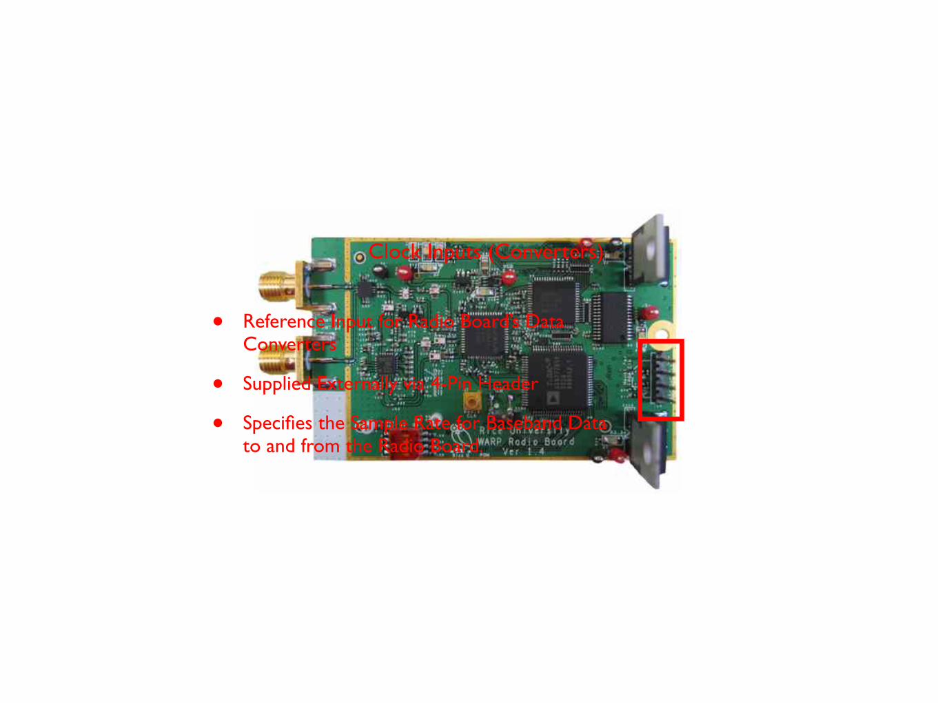
Clock Inputs (Converters)
• Reference Input for Radio Board’s Data Converters
• Supplied Externally via 4-Pin Header
• Specifies the Sample Rate for Baseband Data to and from the Radio Board.
• FPGA-Radio Interface
• Single-Chip Radio IC
• Clock Inputs
• Other Functions
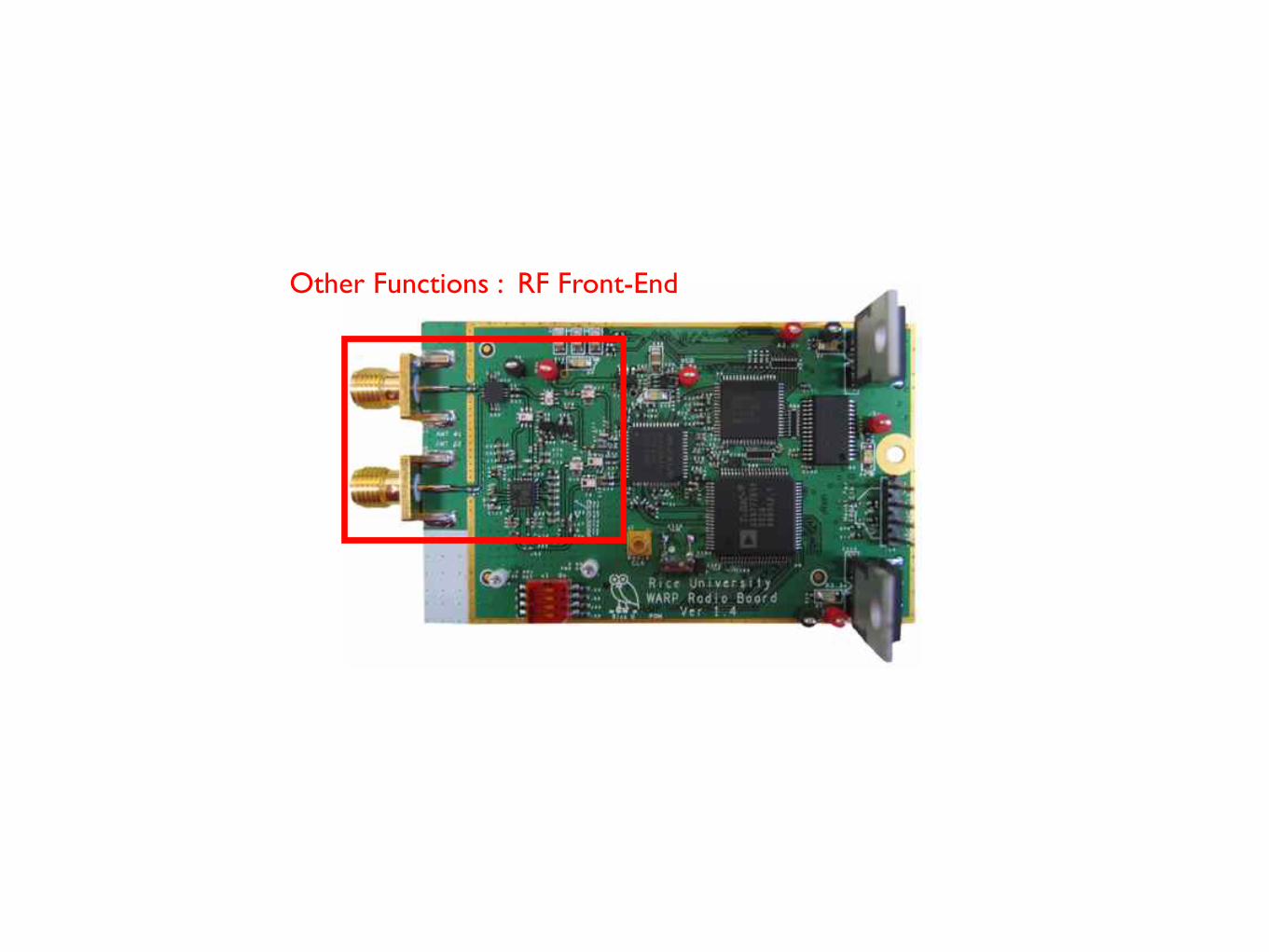
Other Functions : RF Front-End
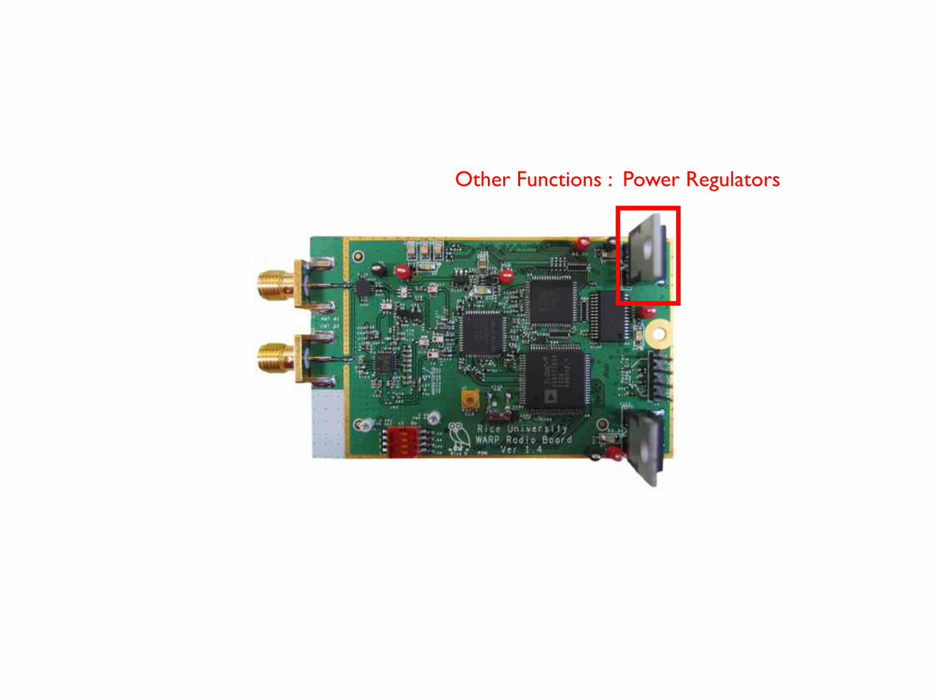
Other Functions : Power Regulators
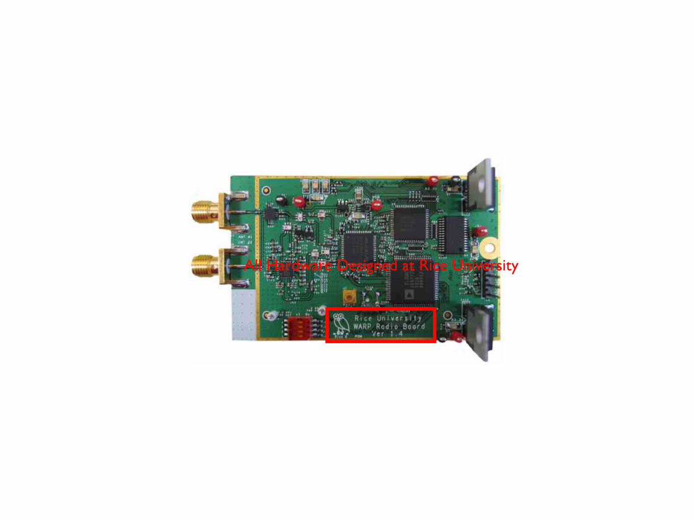
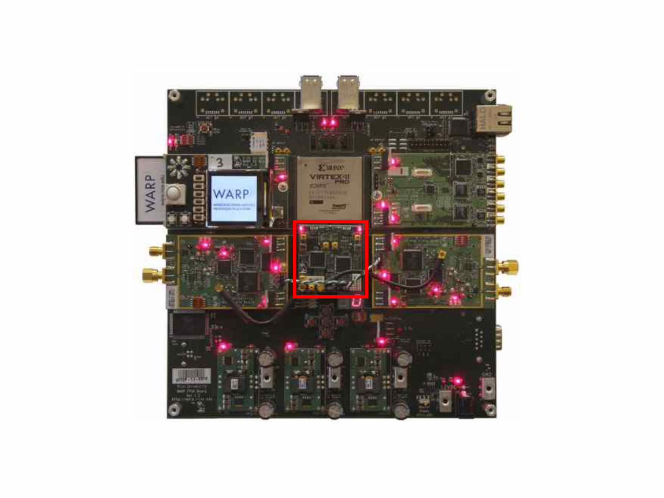
All Hardware Designed at Rice University
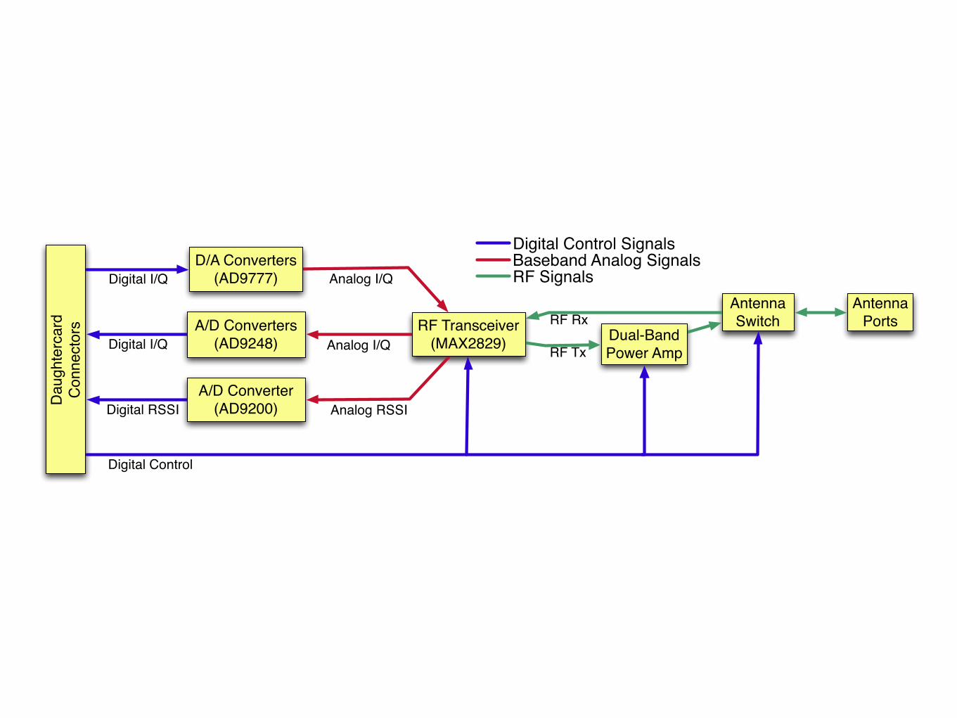
RF Transceiver
(MAX2829)
D/A Converters
(AD9777)
A/D Converters
(AD9248)
A/D Converter
(AD9200)
Dual-Band
Power Amp
Antenna
Switch
Antenna
Ports
Analog I/Q
Analog I/Q
Analog RSSI
RF Tx
RF Rx
Da
ug
hte
rca
rd
Co
nn
ecto
rs
Digital I/Q
Digital I/Q
Digital RSSI
Digital Control
Baseband Analog SignalsDigital Control Signals
RF Signals
Questions?
WARP Hardware
• WARP Board-Level Components
- FPGA Board
- Radio Board
- Clock Board
• WARP FPGA Device Architecture
• WARP Design Flows
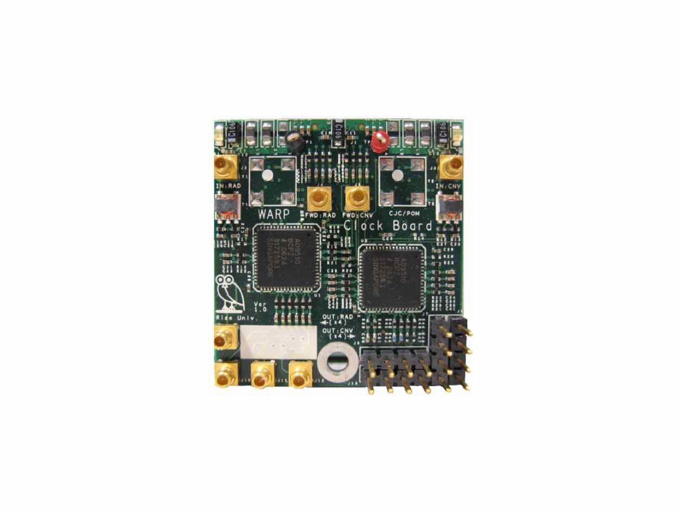
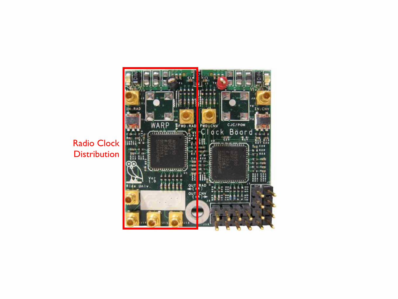
Radio ClockDistribution
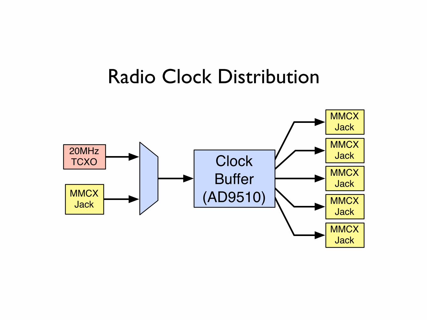
Radio Clock Distribution
Clock
Buffer
(AD9510)MMCXJack
20MHz TCXO
MMCXJack
MMCXJack
MMCXJack
MMCXJack
MMCXJack
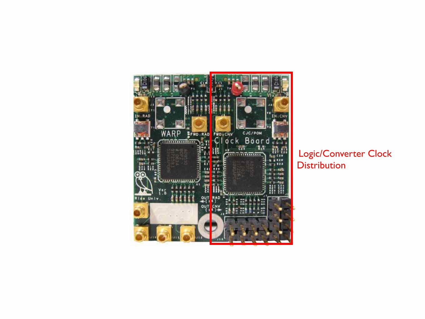
Logic/Converter ClockDistribution
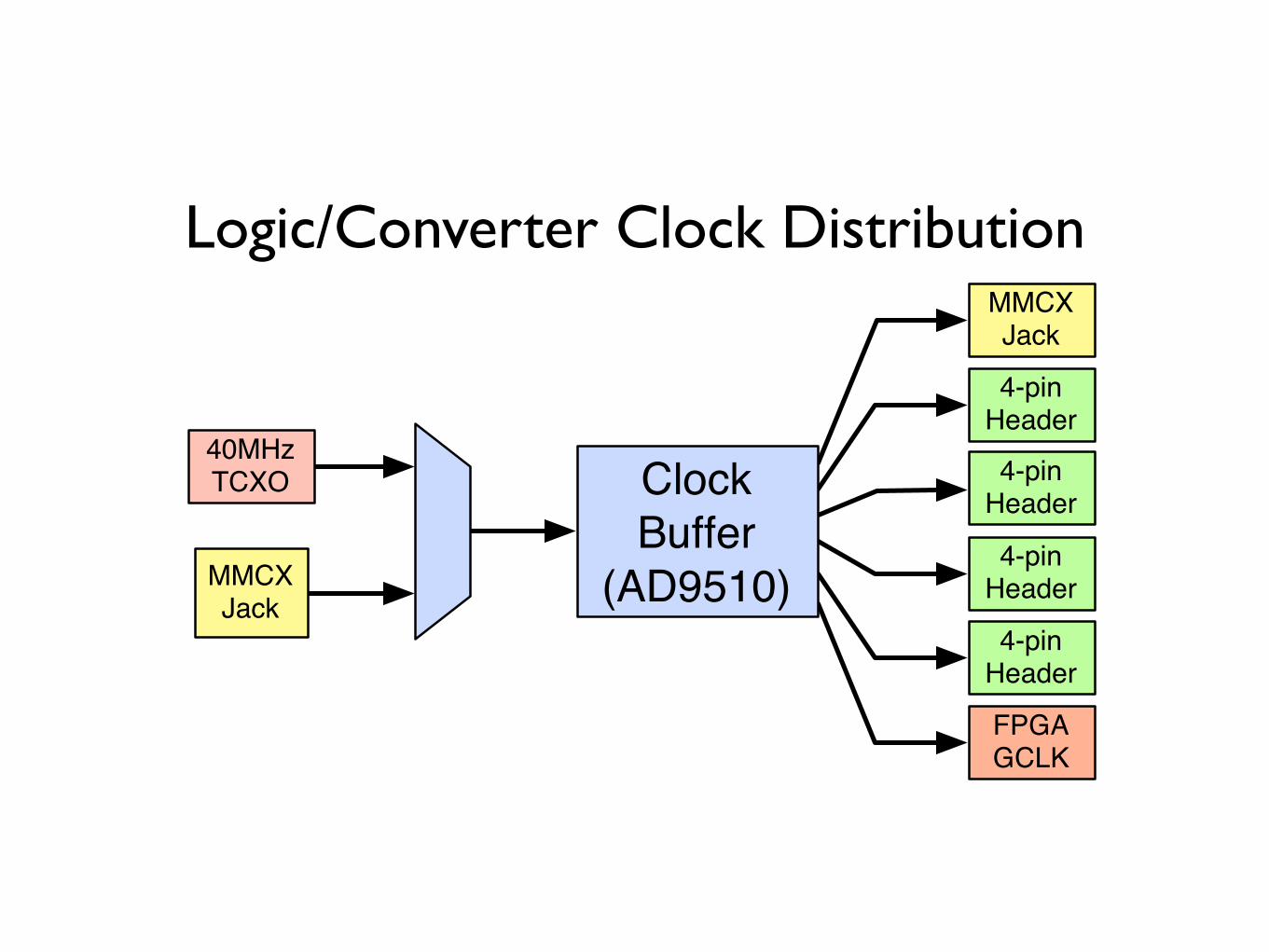
Logic/Converter Clock Distribution
Clock
Buffer
(AD9510)MMCXJack
40MHz TCXO
MMCXJack
4-pinHeader
4-pinHeader
4-pinHeader
4-pinHeader
FPGAGCLK
Questions?
WARP Hardware
• WARP Board-Level Components
- FPGA Board
- Radio Board
- Clock Board
• WARP FPGA Device Architecture
• WARP Design Flows
XC2VP70 Internal Resources
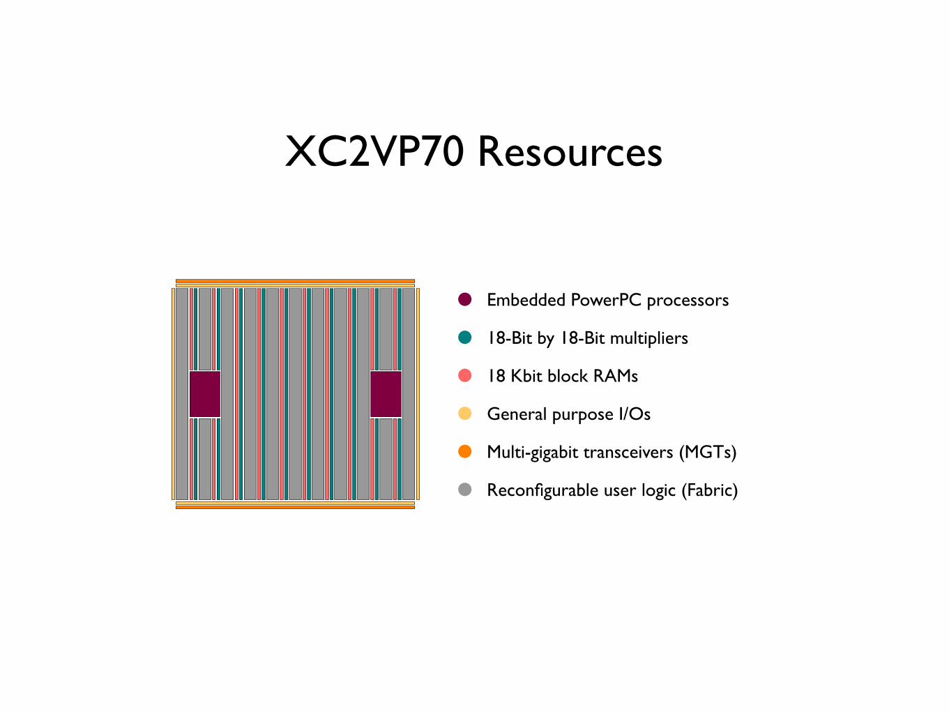
• Embedded PowerPC processors
• 18-Bit by 18-Bit multipliers
• 18 Kbit block RAMs
• General purpose I/Os
• Multi-gigabit transceivers (MGTs)
• Reconfigurable user logic (Fabric)
XC2VP70 Resources
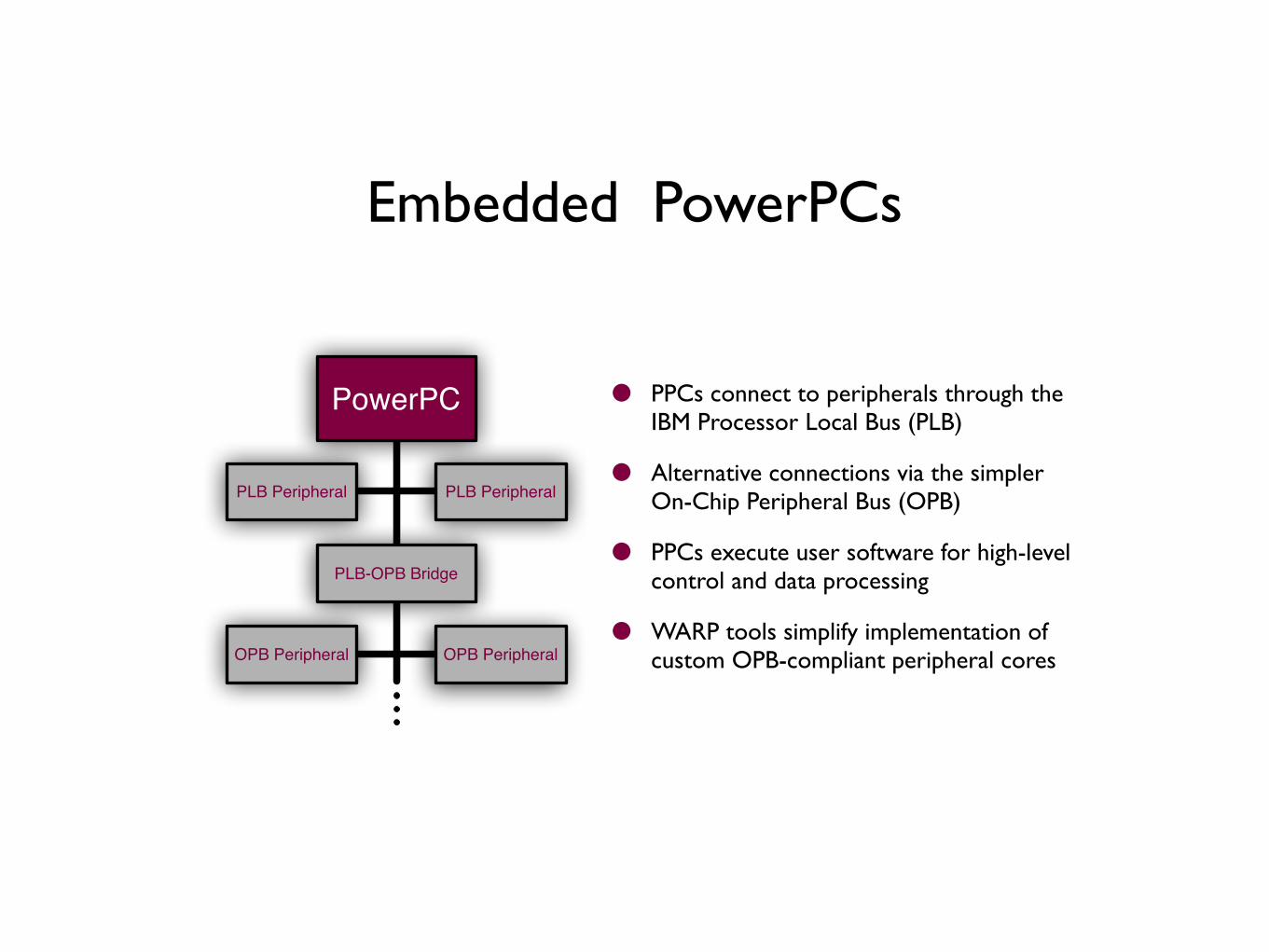
• PPCs connect to peripherals through the IBM Processor Local Bus (PLB)
• Alternative connections via the simpler On-Chip Peripheral Bus (OPB)
• PPCs execute user software for high-level control and data processing
• WARP tools simplify implementation of custom OPB-compliant peripheral cores
Embedded PowerPCs
PowerPC
PLB Peripheral PLB Peripheral
PLB-OPB Bridge
OPB Peripheral OPB Peripheral
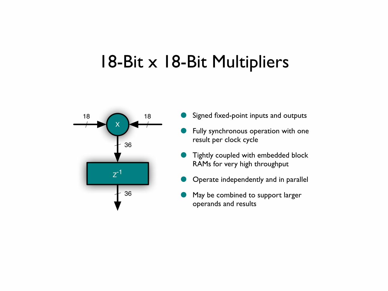
• Signed fixed-point inputs and outputs
• Fully synchronous operation with one result per clock cycle
• Tightly coupled with embedded block RAMs for very high throughput
• Operate independently and in parallel
• May be combined to support larger operands and results
18-Bit x 18-Bit Multipliers
X
Z-1
18 18
36
36
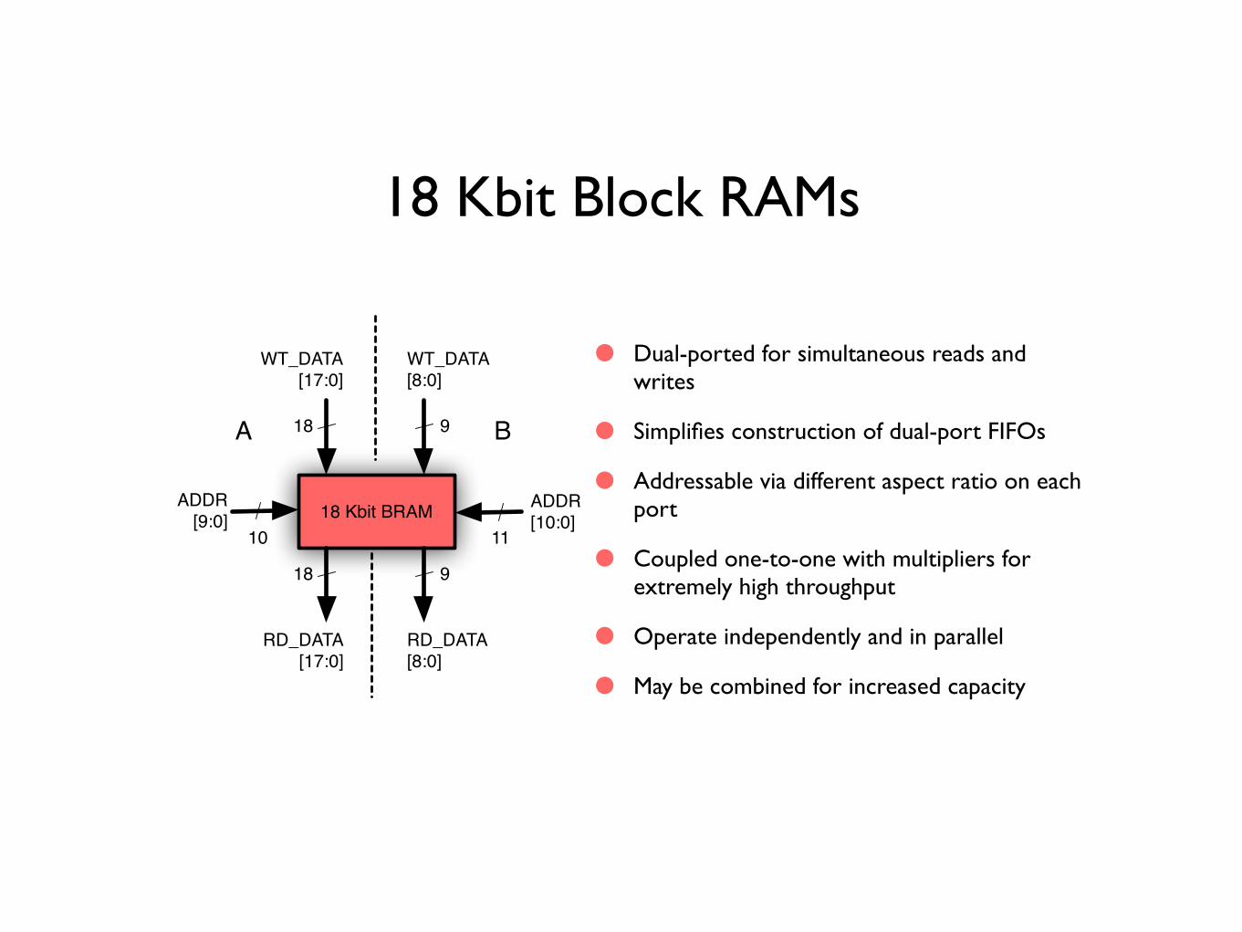
• Dual-ported for simultaneous reads and writes
• Simplifies construction of dual-port FIFOs
• Addressable via different aspect ratio on each port
• Coupled one-to-one with multipliers for extremely high throughput
• Operate independently and in parallel
• May be combined for increased capacity
18 Kbit Block RAMs
18 Kbit BRAM
11
ADDR
[10:0]10
ADDR
[9:0]
18 9
WT_DATA
[17:0]
WT_DATA
[8:0]
18 9
RD_DATA
[17:0]
RD_DATA
[8:0]
A B
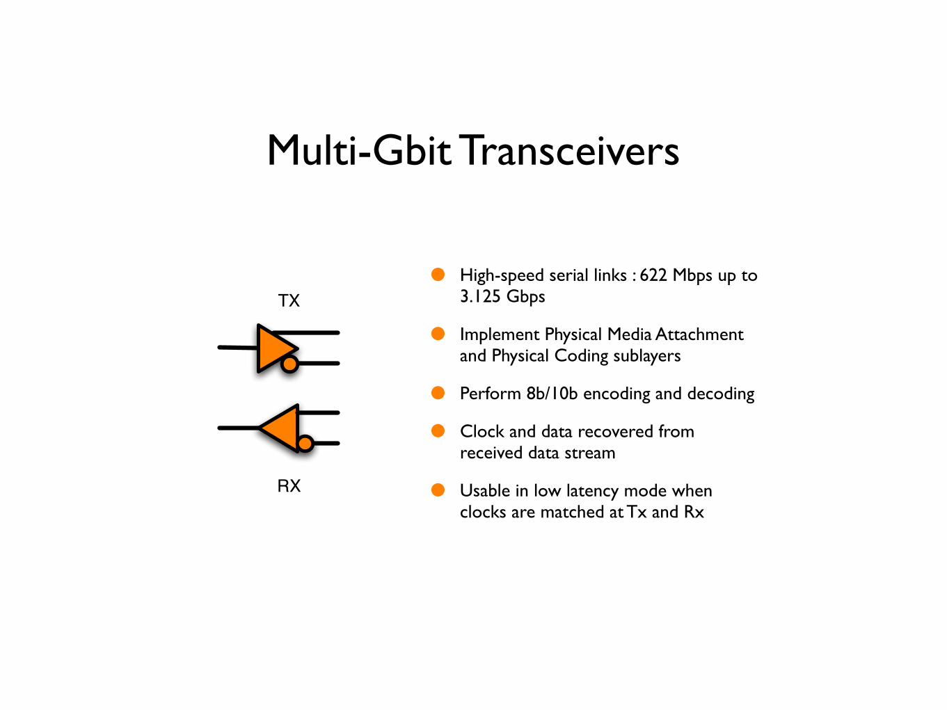
• High-speed serial links : 622 Mbps up to 3.125 Gbps
• Implement Physical Media Attachment and Physical Coding sublayers
• Perform 8b/10b encoding and decoding
• Clock and data recovered from received data stream
• Usable in low latency mode when clocks are matched at Tx and Rx
Multi-Gbit Transceivers
TX
RX
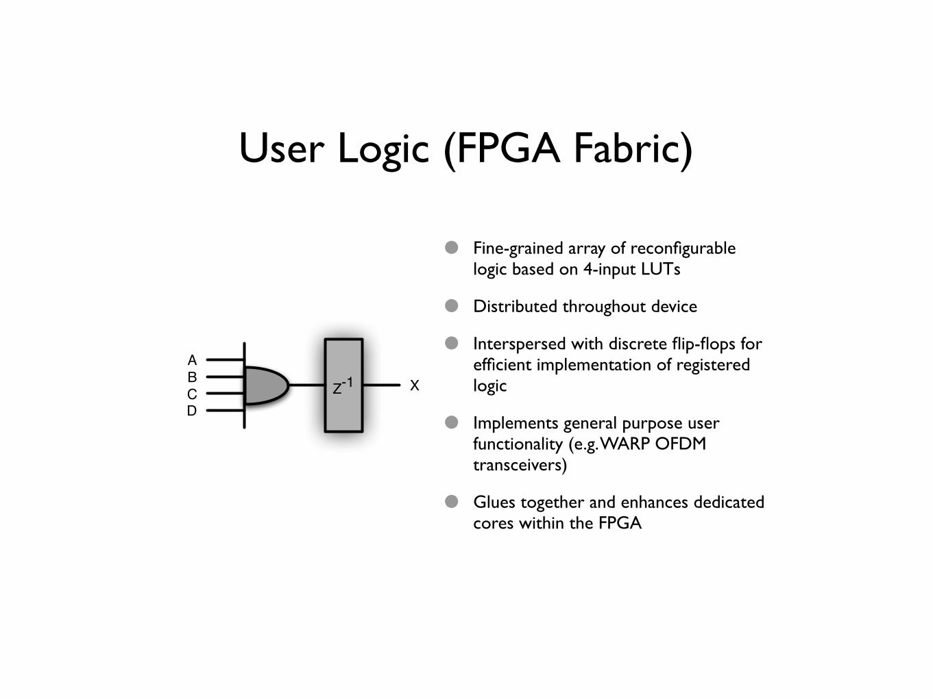
• Fine-grained array of reconfigurable logic based on 4-input LUTs
• Distributed throughout device
• Interspersed with discrete flip-flops for efficient implementation of registered logic
• Implements general purpose user functionality (e.g. WARP OFDM transceivers)
• Glues together and enhances dedicated cores within the FPGA
User Logic (FPGA Fabric)
Z-1
A
B
C
D
X
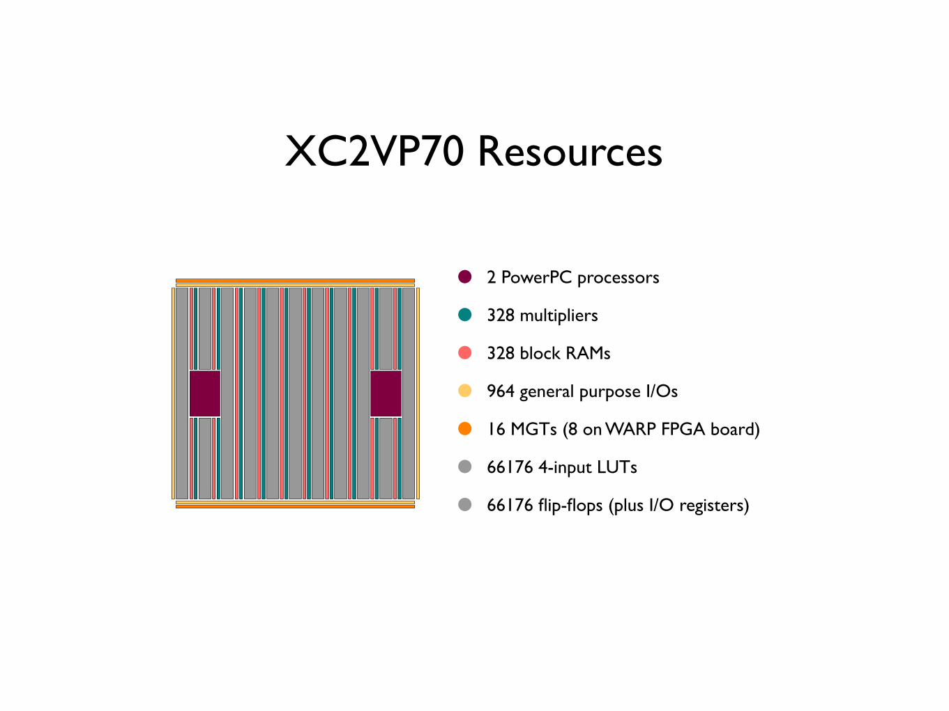
• 2 PowerPC processors
• 328 multipliers
• 328 block RAMs
• 964 general purpose I/Os
• 16 MGTs (8 on WARP FPGA board)
• 66176 4-input LUTs
• 66176 flip-flops (plus I/O registers)
XC2VP70 Resources
Questions?PowerPC
PLB Peripheral PLB Peripheral
PLB-OPB Bridge
OPB Peripheral OPB Peripheral
X
Z-1
18 18
36
36
TX
RX
Z-1
A
B
C
D
X
18 Kbit BRAM
11
ADDR
[10:0]10
ADDR
[9:0]
18 9
WT_DATA
[17:0]
WT_DATA
[8:0]
18 9
RD_DATA
[17:0]
RD_DATA
[8:0]
A B
WARP Hardware
• WARP Board-Level Components
- FPGA Board
- Radio Board
- Clock Board
• WARP FPGA Device Architecture
• WARP Design Flows
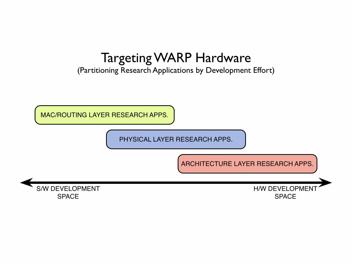
Targeting WARP Hardware(Partitioning Research Applications by Development Effort)
MAC/ROUTING LAYER RESEARCH APPS.
H/W DEVELOPMENT
SPACE
PHYSICAL LAYER RESEARCH APPS.
ARCHITECTURE LAYER RESEARCH APPS.
S/W DEVELOPMENT
SPACE
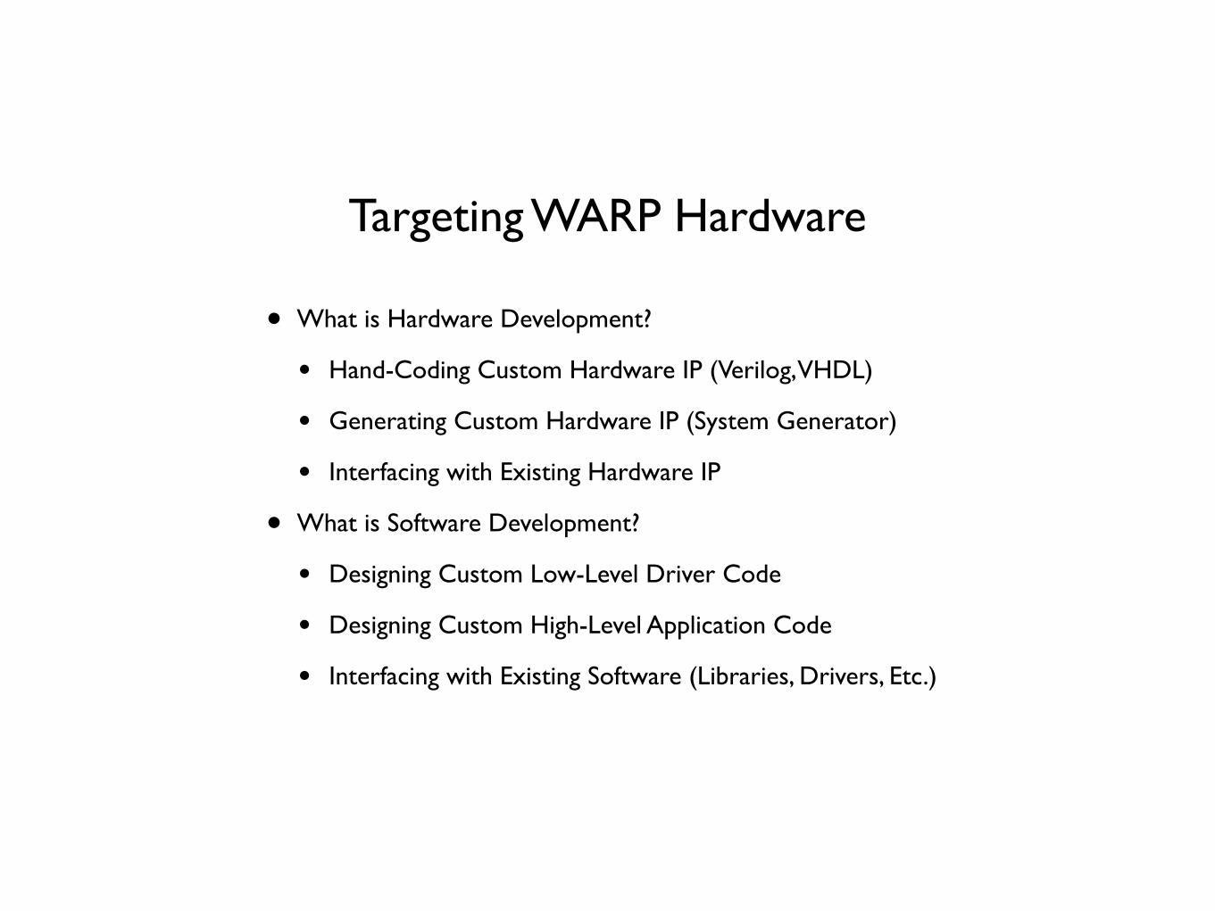
Targeting WARP Hardware
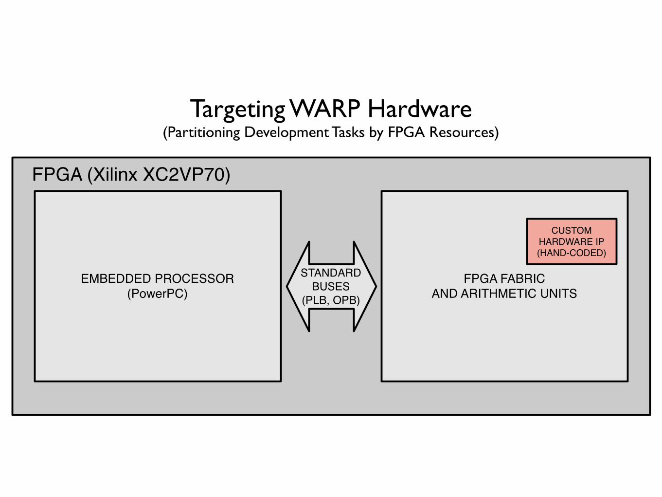
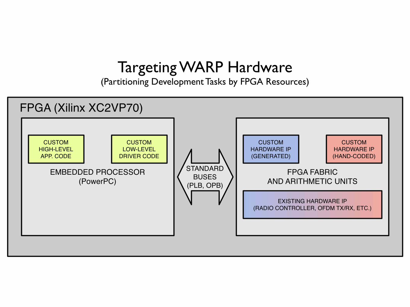
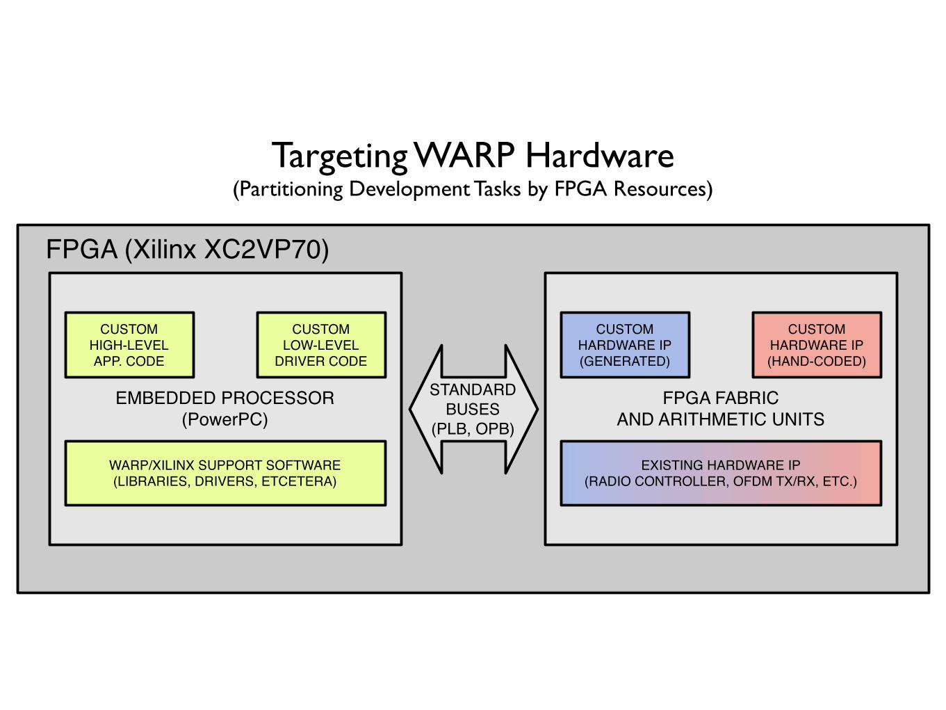
• What is Hardware Development?
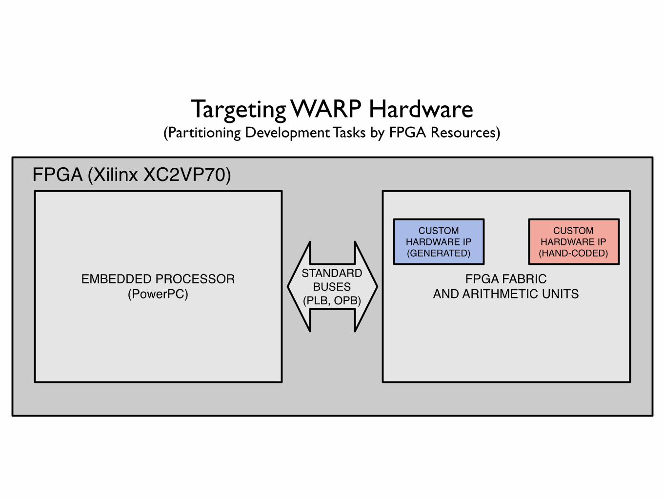
• Hand-Coding Custom Hardware IP (Verilog, VHDL)
• Generating Custom Hardware IP (System Generator)
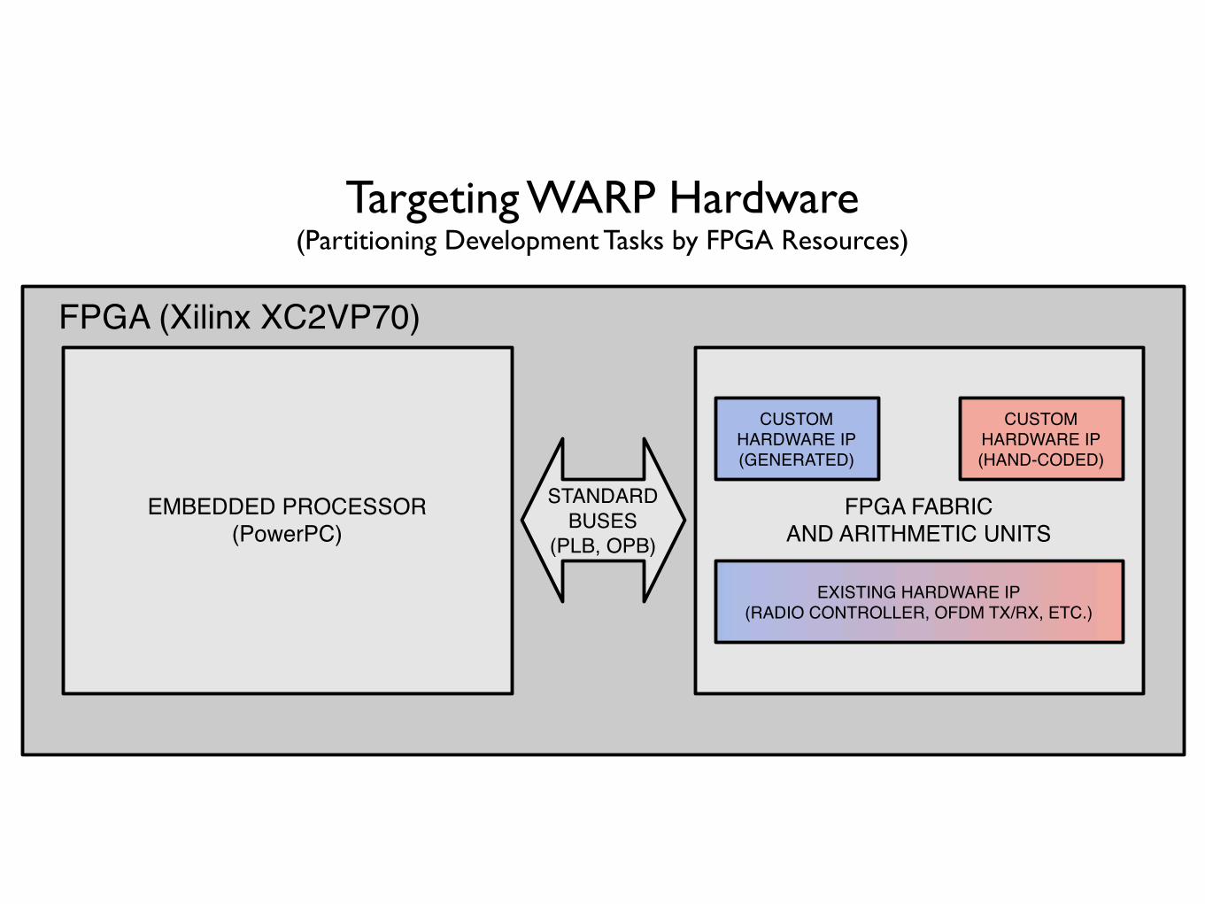
• Interfacing with Existing Hardware IP
• What is Software Development?
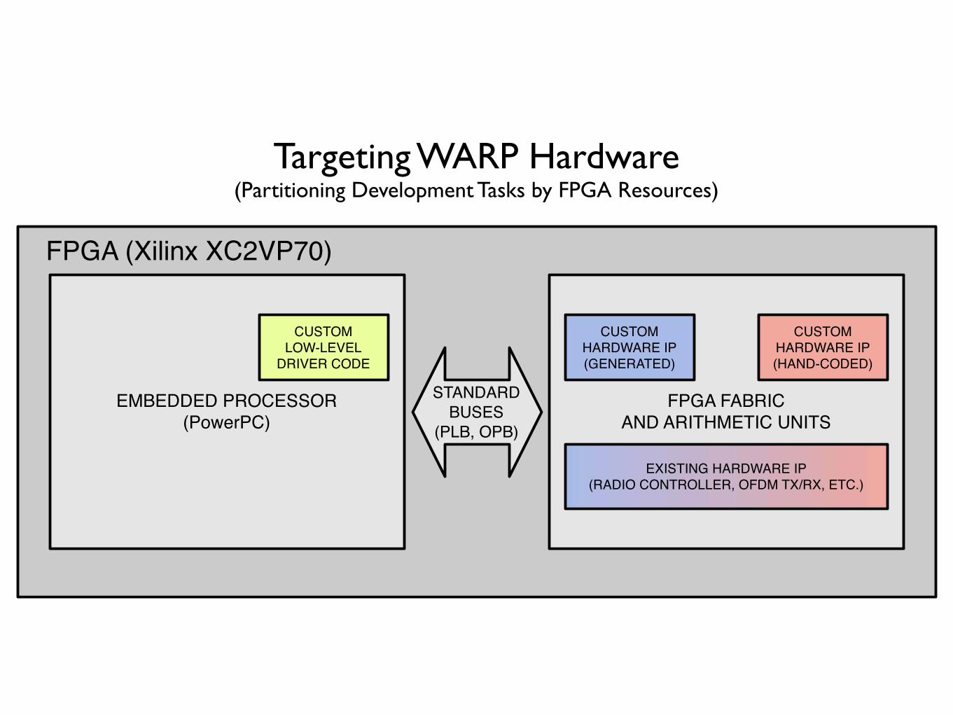
• Designing Custom Low-Level Driver Code
• Designing Custom High-Level Application Code
• Interfacing with Existing Software (Libraries, Drivers, Etc.)
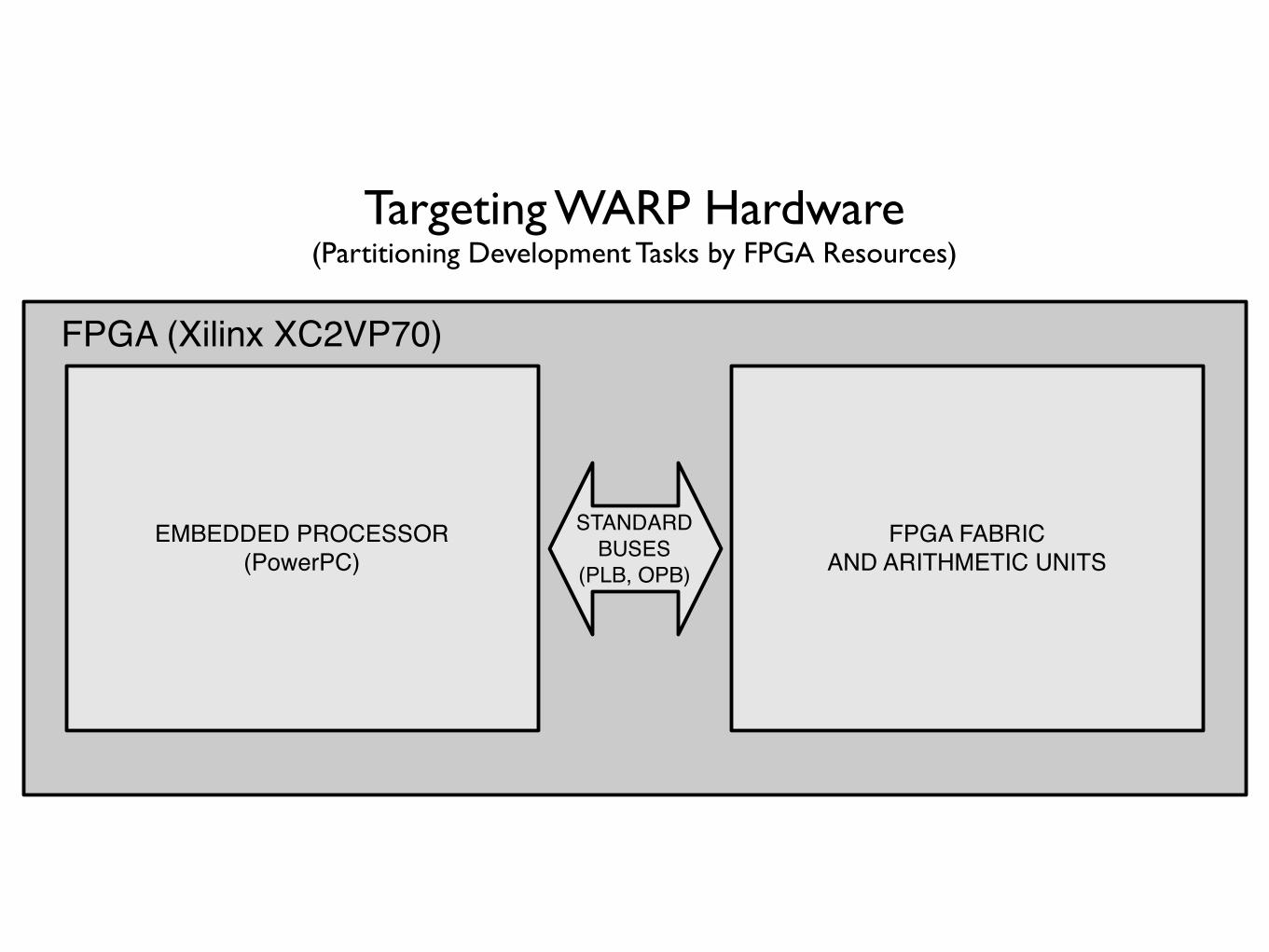
Targeting WARP Hardware(Partitioning Development Tasks by FPGA Resources)
FPGA FABRIC
AND ARITHMETIC UNITS
EMBEDDED PROCESSOR
(PowerPC)
STANDARD
BUSES
(PLB, OPB)
FPGA (Xilinx XC2VP70)
Targeting WARP Hardware(Partitioning Development Tasks by FPGA Resources)
FPGA FABRIC
AND ARITHMETIC UNITS
EMBEDDED PROCESSOR
(PowerPC)
CUSTOM
HARDWARE IP
(HAND-CODED)
STANDARD
BUSES
(PLB, OPB)
FPGA (Xilinx XC2VP70)
Targeting WARP Hardware(Partitioning Development Tasks by FPGA Resources)
FPGA FABRIC
AND ARITHMETIC UNITS
EMBEDDED PROCESSOR
(PowerPC)
CUSTOM
HARDWARE IP
(GENERATED)
CUSTOM
HARDWARE IP
(HAND-CODED)
STANDARD
BUSES
(PLB, OPB)
FPGA (Xilinx XC2VP70)
Targeting WARP Hardware(Partitioning Development Tasks by FPGA Resources)
FPGA FABRIC
AND ARITHMETIC UNITS
EMBEDDED PROCESSOR
(PowerPC)
CUSTOM
HARDWARE IP
(GENERATED)
CUSTOM
HARDWARE IP
(HAND-CODED)
EXISTING HARDWARE IP
(RADIO CONTROLLER, OFDM TX/RX, ETC.)
STANDARD
BUSES
(PLB, OPB)
FPGA (Xilinx XC2VP70)
Targeting WARP Hardware(Partitioning Development Tasks by FPGA Resources)
FPGA FABRIC
AND ARITHMETIC UNITS
EMBEDDED PROCESSOR
(PowerPC)
CUSTOM
LOW-LEVEL
DRIVER CODE
CUSTOM
HARDWARE IP
(GENERATED)
CUSTOM
HARDWARE IP
(HAND-CODED)
EXISTING HARDWARE IP
(RADIO CONTROLLER, OFDM TX/RX, ETC.)
STANDARD
BUSES
(PLB, OPB)
FPGA (Xilinx XC2VP70)
Targeting WARP Hardware(Partitioning Development Tasks by FPGA Resources)
FPGA FABRIC
AND ARITHMETIC UNITS
EMBEDDED PROCESSOR
(PowerPC)
CUSTOM
HIGH-LEVEL
APP. CODE
CUSTOM
LOW-LEVEL
DRIVER CODE
WARP/XILINX SUPPORT SOFTWARE
(LIBRARIES, DRIVERS, ETCETERA)
CUSTOM
HARDWARE IP
(GENERATED)
CUSTOM
HARDWARE IP
(HAND-CODED)
EXISTING HARDWARE IP
(RADIO CONTROLLER, OFDM TX/RX, ETC.)
STANDARD
BUSES
(PLB, OPB)
FPGA (Xilinx XC2VP70)

Targeting WARP Hardware(Partitioning Research Applications by Development Effort)
MAC/ROUTING LAYER RESEARCH APPS.
H/W DEVELOPMENT
SPACE
PHYSICAL LAYER RESEARCH APPS.
ARCHITECTURE LAYER RESEARCH APPS.
S/W DEVELOPMENT
SPACE
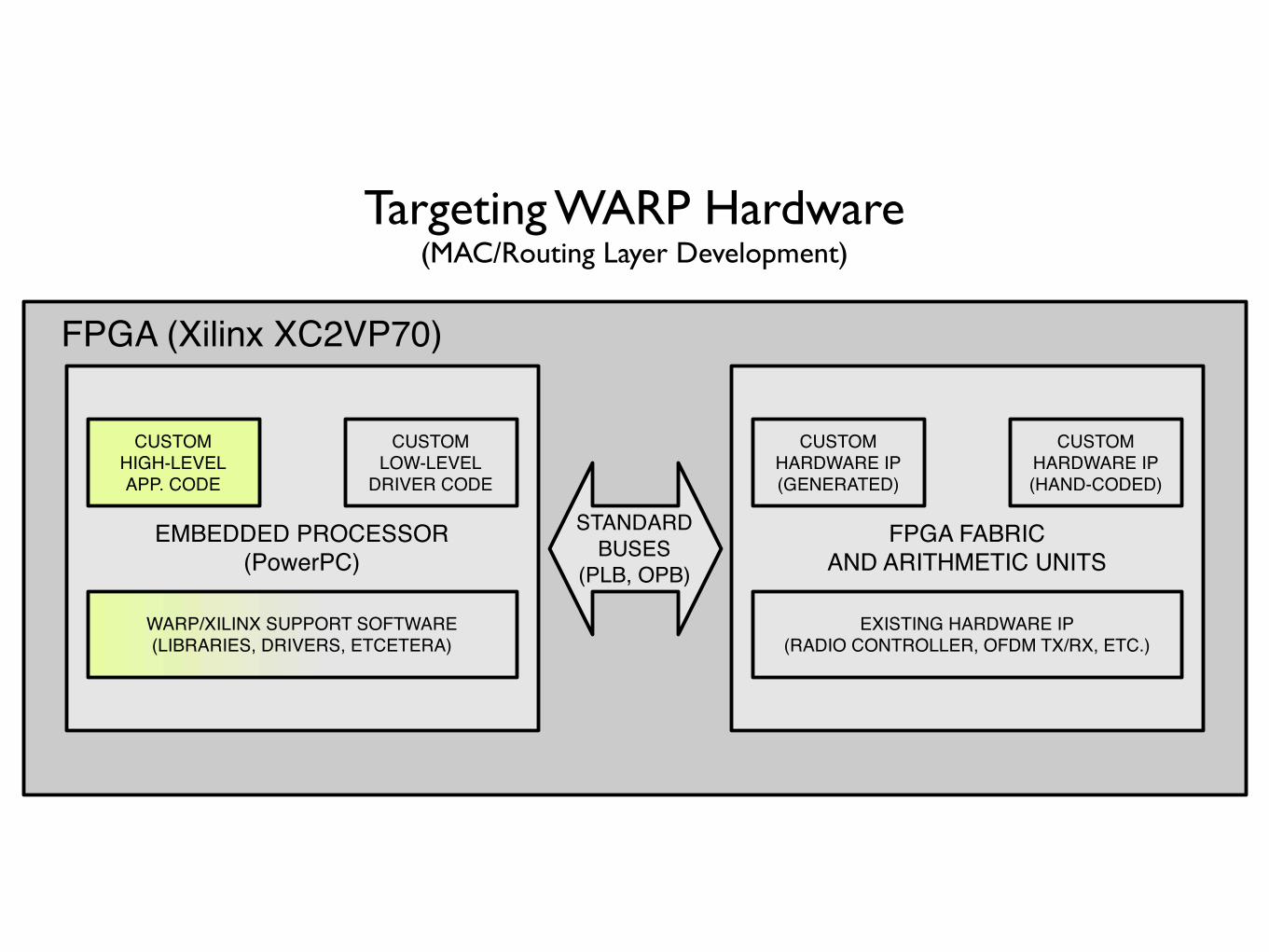
Targeting WARP Hardware(MAC/Routing Layer Development)
FPGA FABRIC
AND ARITHMETIC UNITS
EMBEDDED PROCESSOR
(PowerPC)
CUSTOM
HIGH-LEVEL
APP. CODE
CUSTOM
LOW-LEVEL
DRIVER CODE
WARP/XILINX SUPPORT SOFTWARE
(LIBRARIES, DRIVERS, ETCETERA)
CUSTOM
HARDWARE IP
(GENERATED)
CUSTOM
HARDWARE IP
(HAND-CODED)
EXISTING HARDWARE IP
(RADIO CONTROLLER, OFDM TX/RX, ETC.)
STANDARD
BUSES
(PLB, OPB)
FPGA (Xilinx XC2VP70)
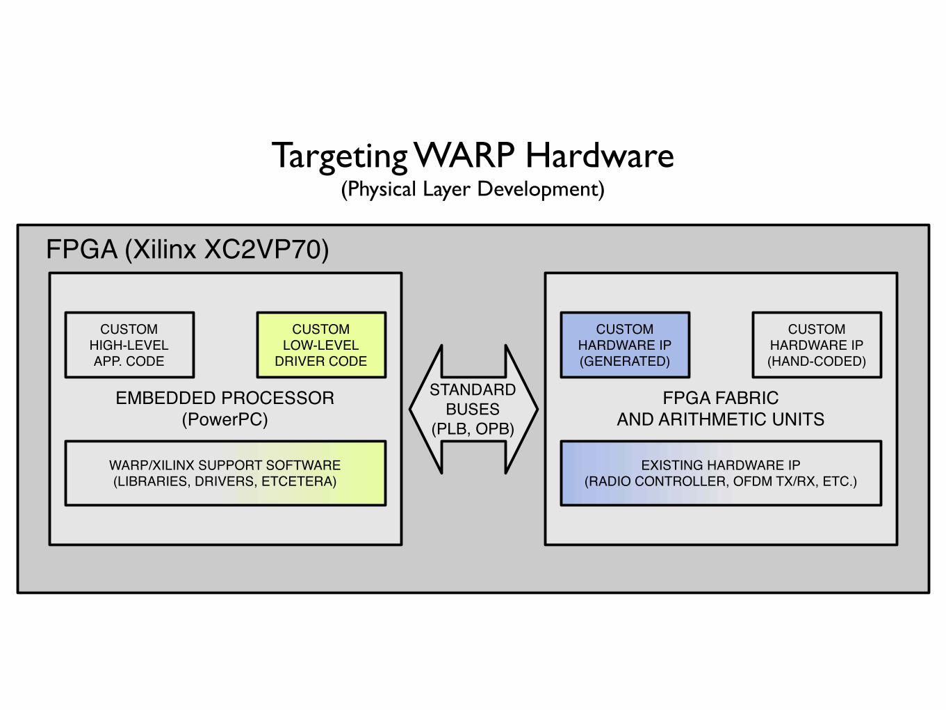
Targeting WARP Hardware(Physical Layer Development)
FPGA FABRIC
AND ARITHMETIC UNITS
EMBEDDED PROCESSOR
(PowerPC)
CUSTOM
HIGH-LEVEL
APP. CODE
CUSTOM
LOW-LEVEL
DRIVER CODE
WARP/XILINX SUPPORT SOFTWARE
(LIBRARIES, DRIVERS, ETCETERA)
CUSTOM
HARDWARE IP
(GENERATED)
CUSTOM
HARDWARE IP
(HAND-CODED)
EXISTING HARDWARE IP
(RADIO CONTROLLER, OFDM TX/RX, ETC.)
STANDARD
BUSES
(PLB, OPB)
FPGA (Xilinx XC2VP70)
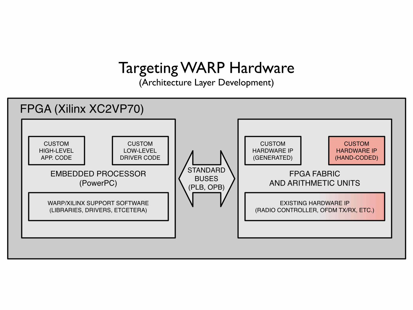
Targeting WARP Hardware(Architecture Layer Development)
FPGA FABRIC
AND ARITHMETIC UNITS
EMBEDDED PROCESSOR
(PowerPC)
CUSTOM
HIGH-LEVEL
APP. CODE
CUSTOM
LOW-LEVEL
DRIVER CODE
WARP/XILINX SUPPORT SOFTWARE
(LIBRARIES, DRIVERS, ETCETERA)
CUSTOM
HARDWARE IP
(GENERATED)
CUSTOM
HARDWARE IP
(HAND-CODED)
EXISTING HARDWARE IP
(RADIO CONTROLLER, OFDM TX/RX, ETC.)
STANDARD
BUSES
(PLB, OPB)
FPGA (Xilinx XC2VP70)
WARP Hardware
Algorithm Development
& Simulation
Piecewise Transition
to Hardware Model MATLAB
System Generator
Low-Level HDL
Automatic
Implementation
Hardware
Visibility
C/C++ Protocol
Implementation
Platform StudioAutomatic
Implementation
Physical LayerAlgorithms
NetworkProtocols
FPGA
PPC
Cores
Logic
Radio
Radio
Radio
Radio& ASIP Development
Targeting WARP Hardware(Introducing Development Tools)
FPGA FABRIC
AND ARITHMETIC UNITS
EMBEDDED PROCESSOR
(PowerPC)
CUSTOM
HIGH-LEVEL
APP. CODE
CUSTOM
LOW-LEVEL
DRIVER CODE
WARP/XILINX SUPPORT SOFTWARE
(LIBRARIES, DRIVERS, ETCETERA)
CUSTOM
HARDWARE IP
(GENERATED)
CUSTOM
HARDWARE IP
(HAND-CODED)
EXISTING HARDWARE IP
(RADIO CONTROLLER, OFDM TX/RX, ETC.)
STANDARD
BUSES
(PLB, OPB)
FPGA (Xilinx XC2VP70)
Questions?
Lab 1: EDK & Sysgen Intro
• Intro to Xilinx Platform Studio
• Building a simple hardware platform
• Interacting with the WARP hardware
• Intro to System Generator and sysgen2opb
• Creating peripherals in Sysgen
• Using Sysgen peripherals in XPS