Embed Size (px)
Citation preview
Introduction
• Bonding means attaching two objects together with a seal (usually permanent)
• Microtechnology involves various types of bonding processes– Wafer bonding– Wire bonding– Flip chip bonding
2
Used in IC packaging and printed circuit board assembly. Will not be covered in this lecture.
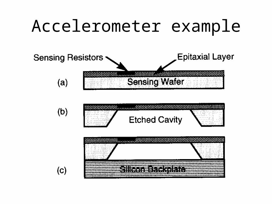
Accelerometer example
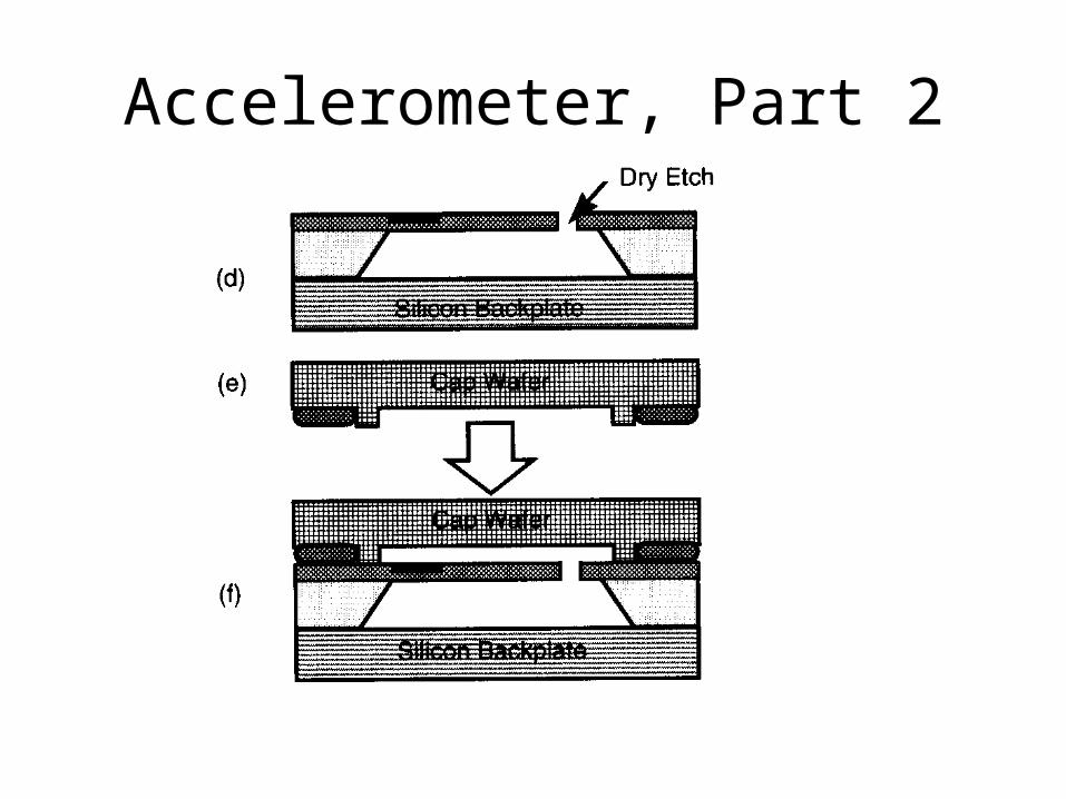
Accelerometer, Part 2
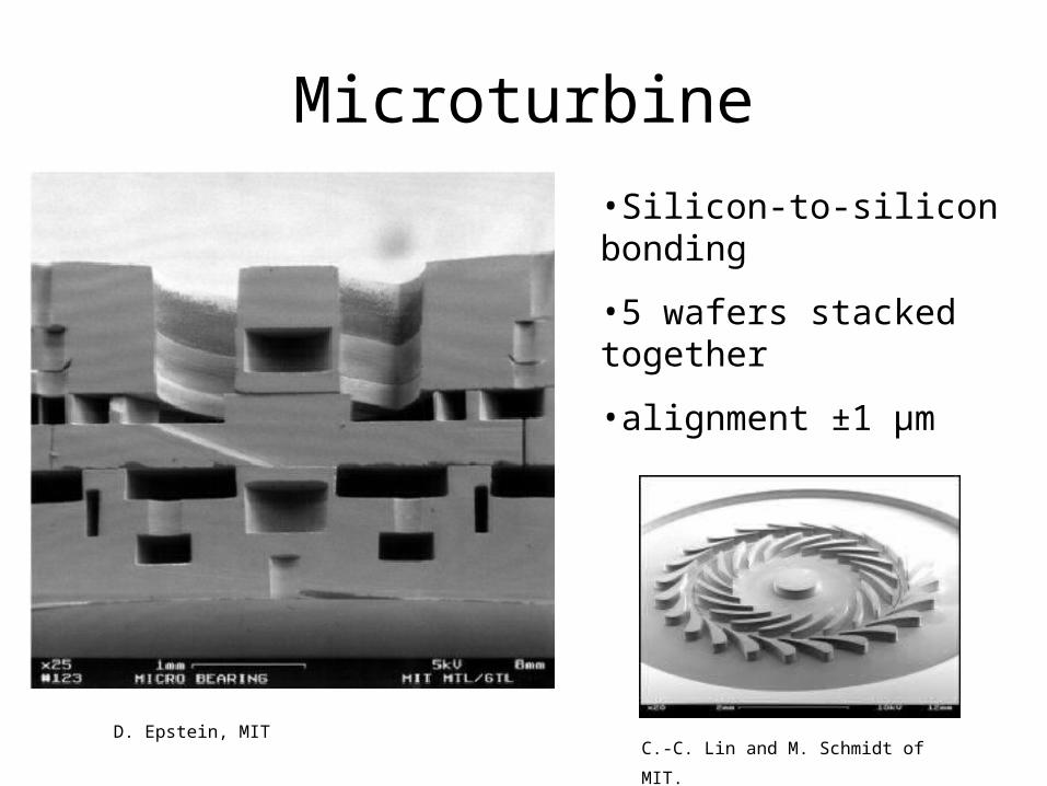
Microturbine
D. Epstein, MIT
•Silicon-to-silicon bonding
•5 wafers stacked together
•alignment ±1 µm
C.-C. Lin and M. Schmidt of MIT.
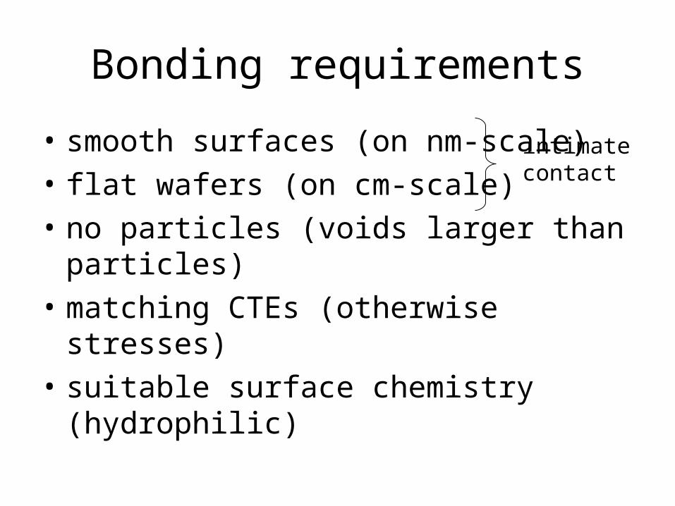
Bonding requirements
• smooth surfaces (on nm-scale)
• flat wafers (on cm-scale)
• no particles (voids larger than particles)
• matching CTEs (otherwise stresses)
• suitable surface chemistry (hydrophilic)
intimate contact
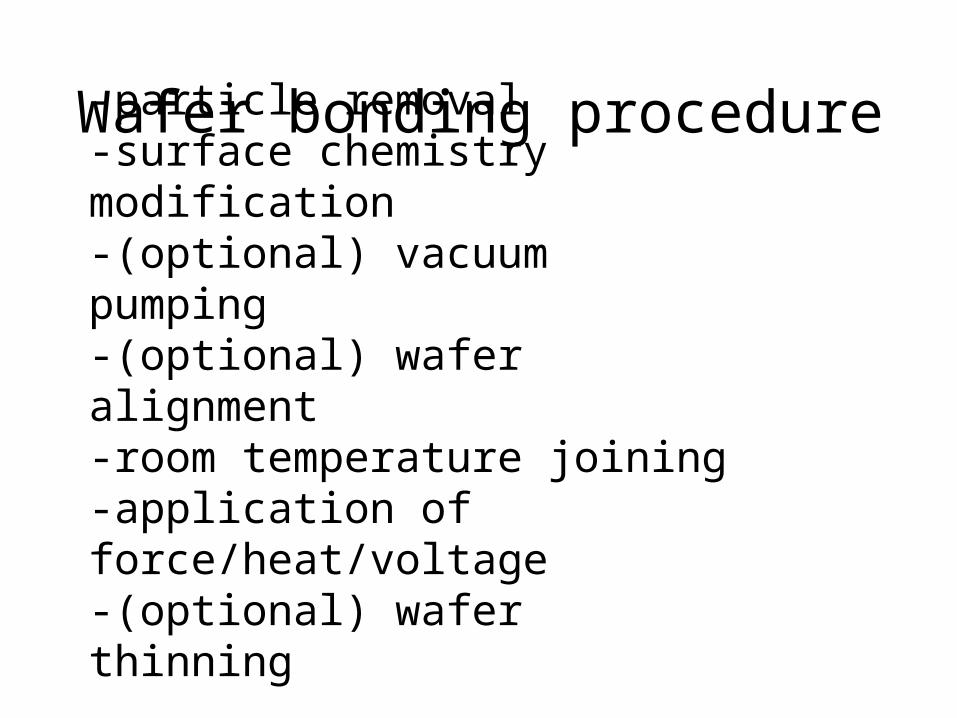
Wafer bonding procedure
-particle removal-surface chemistry modification-(optional) vacuum pumping -(optional) wafer alignment-room temperature joining-application of force/heat/voltage-(optional) wafer thinning
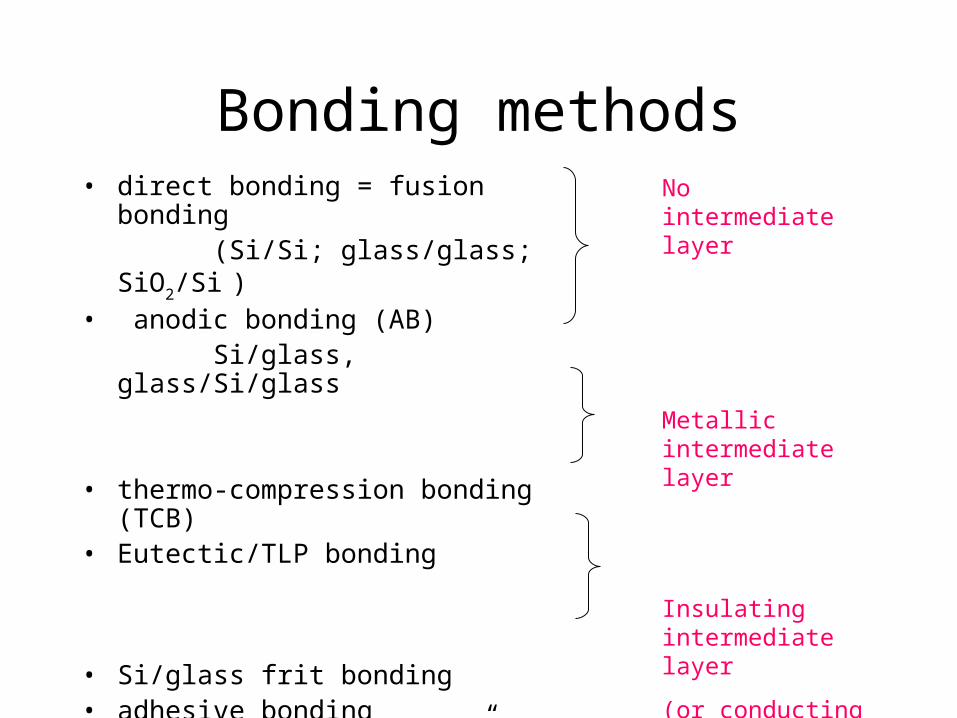
Bonding methods• direct bonding = fusion bonding
(Si/Si; glass/glass; SiO2/Si )• anodic bonding (AB)
Si/glass, glass/Si/glass
• thermo-compression bonding (TCB)• Eutectic/TLP bonding
• Si/glass frit bonding • adhesive bonding
limited by “glue” properties
No intermediate layer
Metallic intermediate layer
Insulating intermediate layer
(or conducting glue)
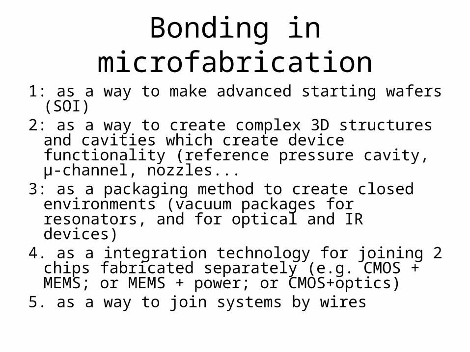
Bonding in microfabrication
1: as a way to make advanced starting wafers (SOI)
2: as a way to create complex 3D structures and cavities which create device functionality (reference pressure cavity, µ-channel, nozzles...
3: as a packaging method to create closed environments (vacuum packages for resonators, and for optical and IR devices)
4. as a integration technology for joining 2 chips fabricated separately (e.g. CMOS + MEMS; or MEMS + power; or CMOS+optics)
5. as a way to join systems by wires
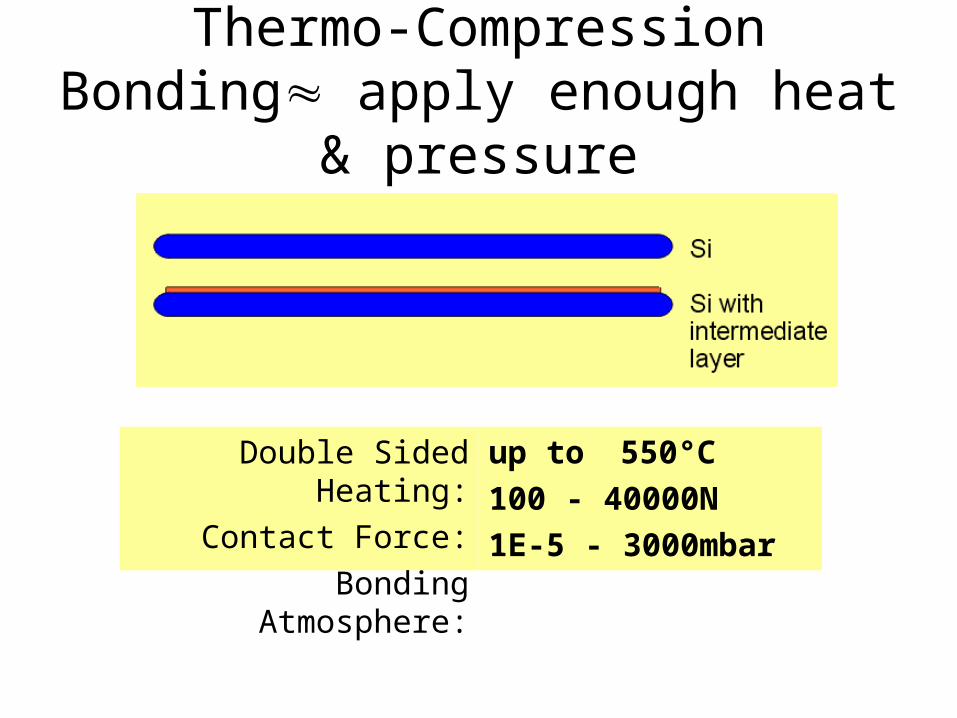
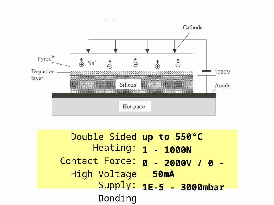
Double Sided Heating:
Contact Force:
Bonding Atmosphere:
up to 550°C
100 - 40000N
1E-5 - 3000mbar
Thermo-Compression Bonding apply enough heat & pressure
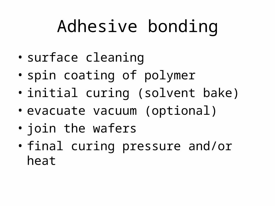
Adhesive bonding
• surface cleaning
• spin coating of polymer
• initial curing (solvent bake)
• evacuate vacuum (optional)
• join the wafers
• final curing pressure and/or heat
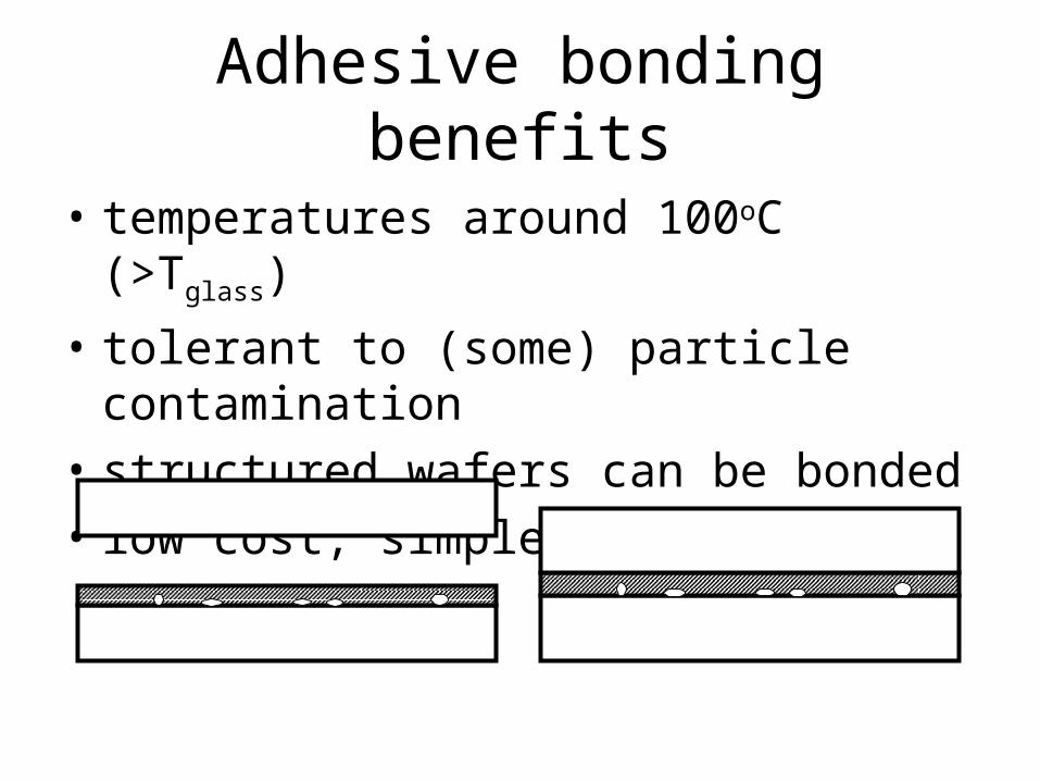
Adhesive bonding benefits
• temperatures around 100oC (>Tglass)
• tolerant to (some) particle contamination
• structured wafers can be bonded
• low cost, simple process
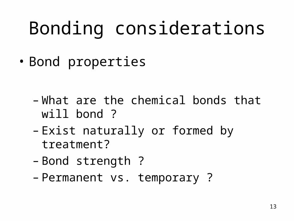
Bonding considerations
• Bond properties
– What are the chemical bonds that will bond ?– Exist naturally or formed by treatment?– Bond strength ?– Permanent vs. temporary ?
13
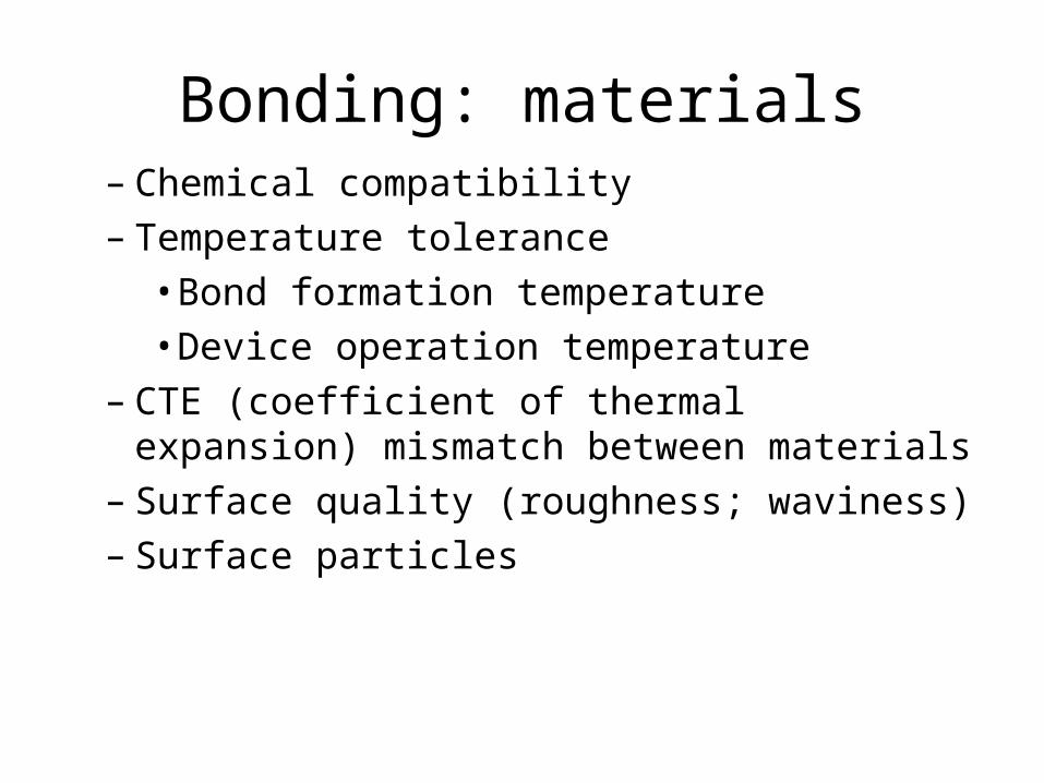
Bonding: materials– Chemical compatibility– Temperature tolerance
• Bond formation temperature• Device operation temperature
– CTE (coefficient of thermal expansion) mismatch between materials
– Surface quality (roughness; waviness)– Surface particles
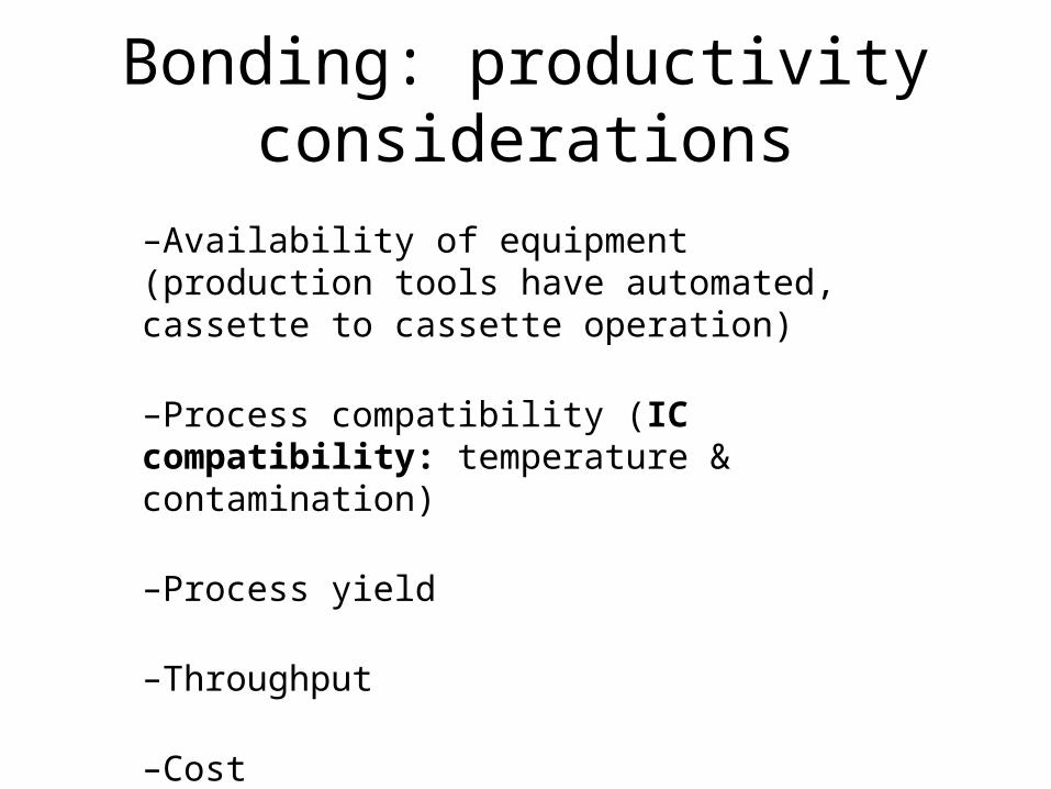
–Availability of equipment (production tools have automated, cassette to cassette operation)
–Process compatibility (IC compatibility: temperature & contamination)
–Process yield
–Throughput
–Cost
–Maturity
Bonding: productivity considerations
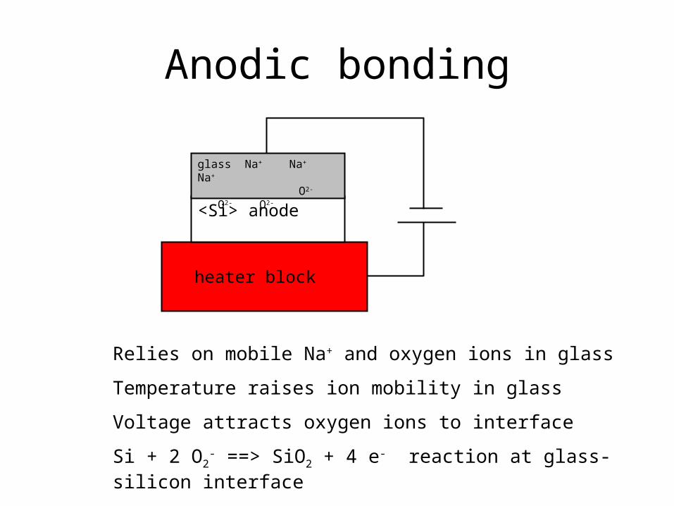
Anodic bonding
<Si> anode
glass Na+ Na+ Na+
O2- O2- O2-
Relies on mobile Na+ and oxygen ions in glass
Temperature raises ion mobility in glass
Voltage attracts oxygen ions to interface
Si + 2 O2- ==> SiO2 + 4 e- reaction at glass-silicon interface
heater block
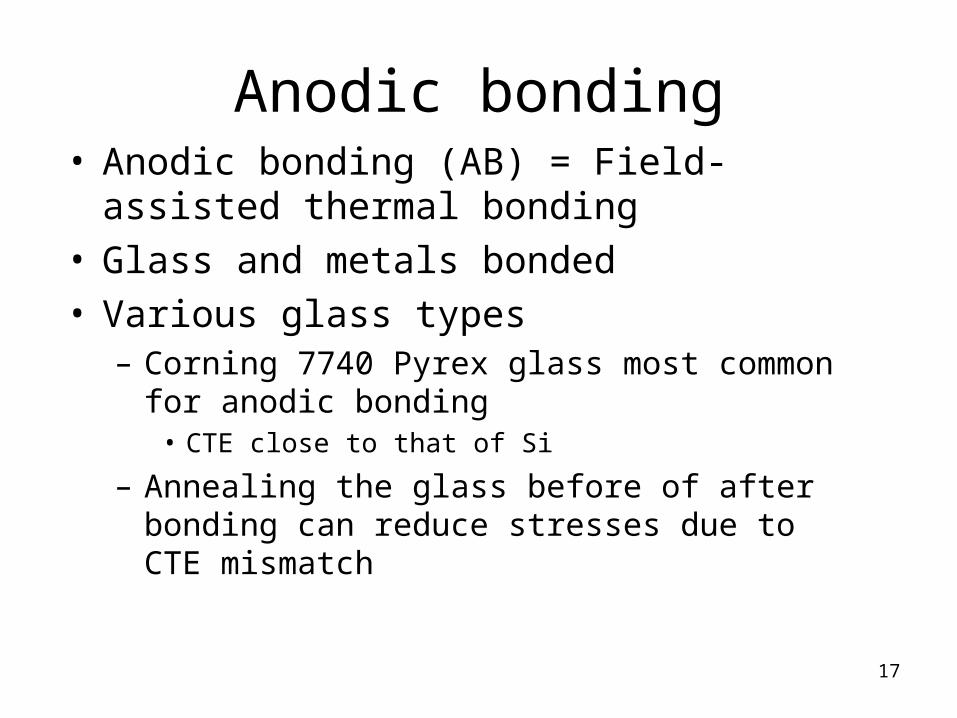
Anodic bonding• Anodic bonding (AB) = Field-assisted thermal
bonding• Glass and metals bonded• Various glass types
– Corning 7740 Pyrex glass most common for anodic bonding
• CTE close to that of Si
– Annealing the glass before of after bonding can reduce stresses due to CTE mismatch
17
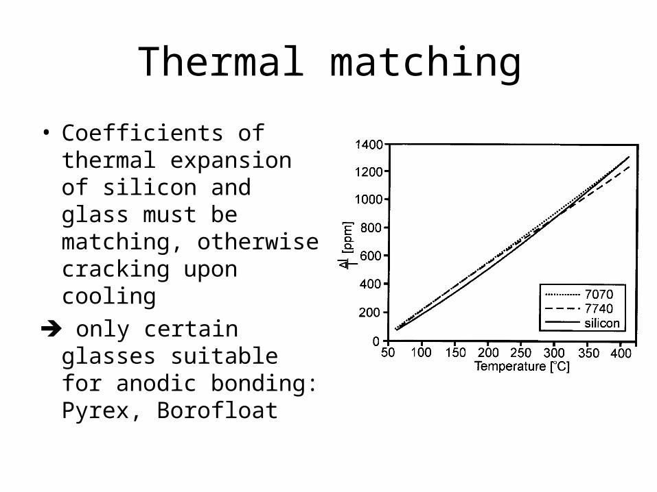
Thermal matching
• Coefficients of thermal expansion of silicon and glass must be matching, otherwise cracking upon cooling
only certain glasses suitable for anodic bonding: Pyrex, Borofloat
Anodic bonding
Double Sided Heating:
Contact Force:
High Voltage Supply:
Bonding Atmosphere:
up to 550°C
1 - 1000N
0 - 2000V / 0 - 50mA
1E-5 - 3000mbar
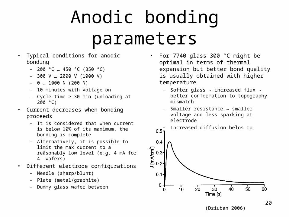
Anodic bonding parameters• Typical conditions for anodic bonding
– 200 °C … 450 °C (350 °C)– 300 V … 2000 V (1000 V)– 0 … 1000 N (200 N)– 10 minutes with voltage on– Cycle time > 30 min (unloading at
200 °C)
• Current decreases when bonding proceeds
– It is considered that when current is below 10% of its maximum, the bonding is complete
– Alternatively, it is possible to limit the max current to a reasonably low level (e.g. 4 mA for 4” wafers)
• Different electrode configurations– Needle (sharp/blunt)– Plate (metal/graphite)– Dummy glass wafer between
20(Dziuban 2006)
• For 7740 glass 300 °C might be optimal in terms of thermal expansion but better bond quality is usually obtained with higher temperature
– Softer glass → increased flux → better conformation to topography mismatch
– Smaller resistance → smaller voltage and less sparking at electrode
– Increased diffusion helps to remove contaminants
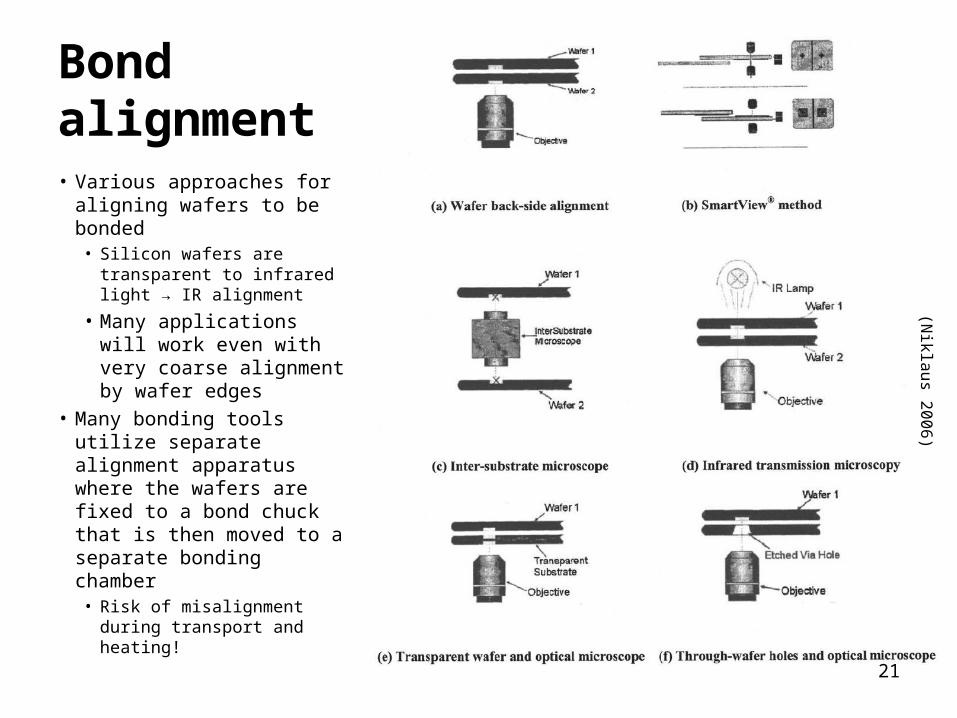
Bond alignment• Various approaches for
aligning wafers to be bonded• Silicon wafers are transparent
to infrared light → IR alignment
• Many applications will work even with very coarse alignment by wafer edges
• Many bonding tools utilize separate alignment apparatus where the wafers are fixed to a bond chuck that is then moved to a separate bonding chamber• Risk of misalignment during
transport and heating!
21
(Niklaus 2006)
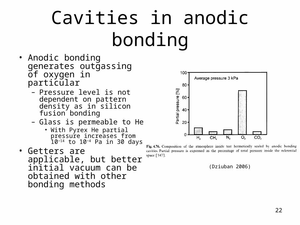
Cavities in anodic bonding
• Anodic bonding generates outgassing of oxygen in particular– Pressure level is not
dependent on pattern density as in silicon fusion bonding
– Glass is permeable to He• With Pyrex He partial
pressure increases from 10−14 to 10−4 Pa in 30 days
• Getters are applicable, but better initial vacuum can be obtained with other bonding methods
22
(Dziuban 2006)
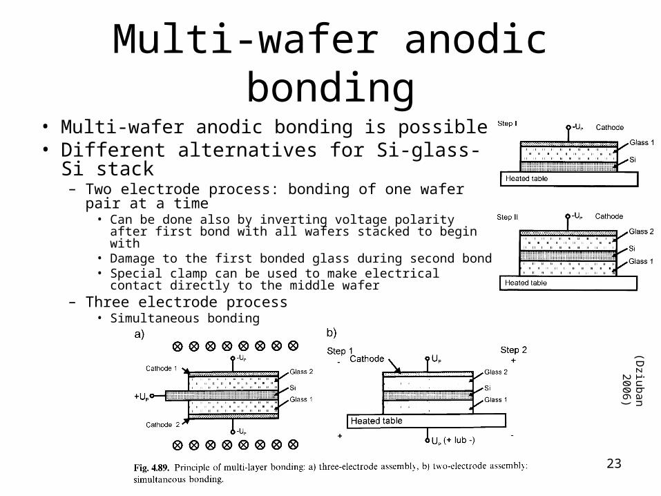
Multi-wafer anodic bonding
• Multi-wafer anodic bonding is possible• Different alternatives for Si-glass-Si stack
– Two electrode process: bonding of one wafer pair at a time
• Can be done also by inverting voltage polarity after first bond with all wafers stacked to begin with
• Damage to the first bonded glass during second bond• Special clamp can be used to make electrical contact
directly to the middle wafer– Three electrode process
• Simultaneous bonding
23
(Dziuban 2006)
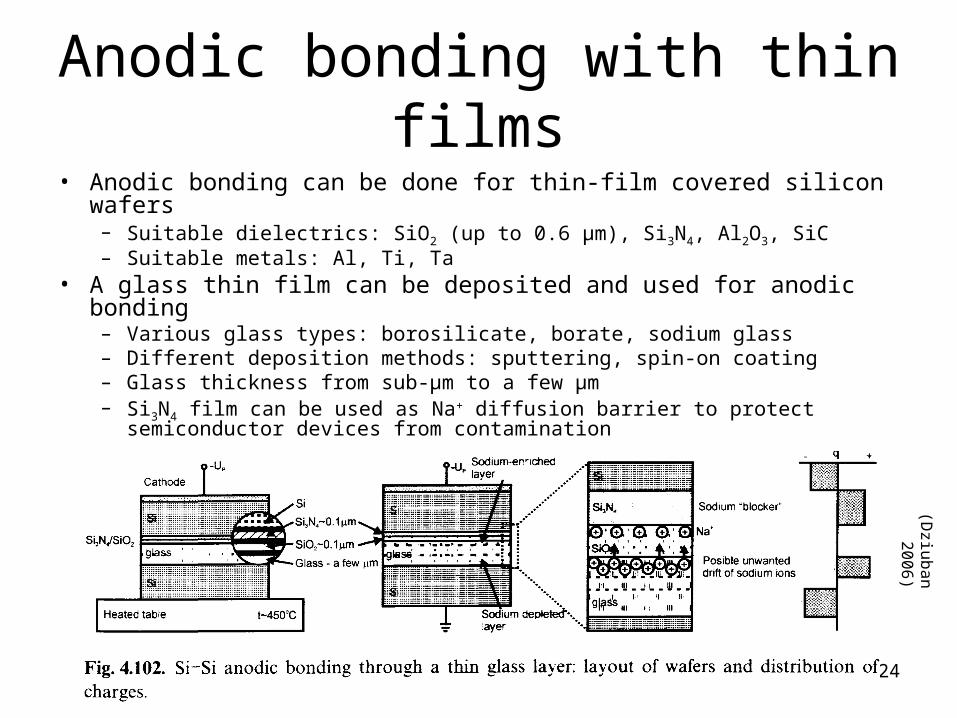
Anodic bonding with thin films• Anodic bonding can be done for thin-film covered silicon wafers
– Suitable dielectrics: SiO2 (up to 0.6 µm), Si3N4, Al2O3, SiC– Suitable metals: Al, Ti, Ta
• A glass thin film can be deposited and used for anodic bonding– Various glass types: borosilicate, borate, sodium glass– Different deposition methods: sputtering, spin-on coating– Glass thickness from sub-µm to a few µm– Si3N4 film can be used as Na+ diffusion barrier to protect semiconductor
devices from contamination
24
(Dziuban 2006)
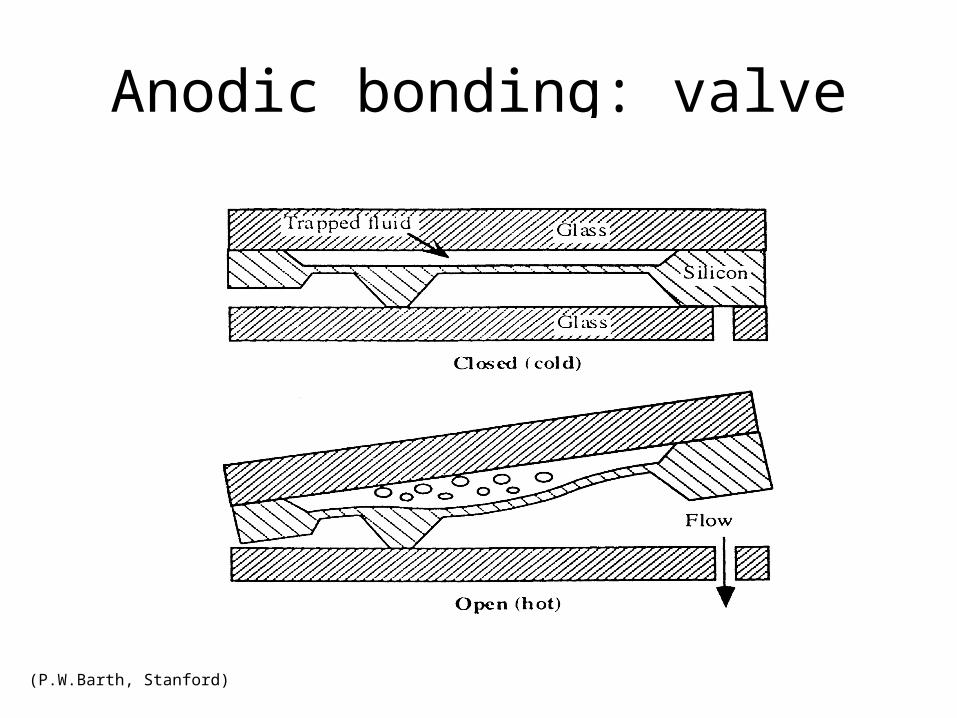
Anodic bonding: valve
(P.W.Barth, Stanford)
Fusion/direct/thermal bonding
• Identical materials bonded
• No CTE problems
• Bonds naturally available
• Apply heat/pressure to enhance bonding
• Si-Si
• Glass-glass
• Polymer-polymer
Polymer thermal bonding
• Raise temperature above Tg
softening
intimate contact (hold long enough)cool down below TgBond interface indistinguishable from bulk
materials (because same bonds !)
Polymer bonding (2)
Softening by solvent surface treatment
Intimate contact (hold long enough)Bonding of different polymers, too!
In theory a room temperature processIn practise difficult to control the thickness
of the softened layer
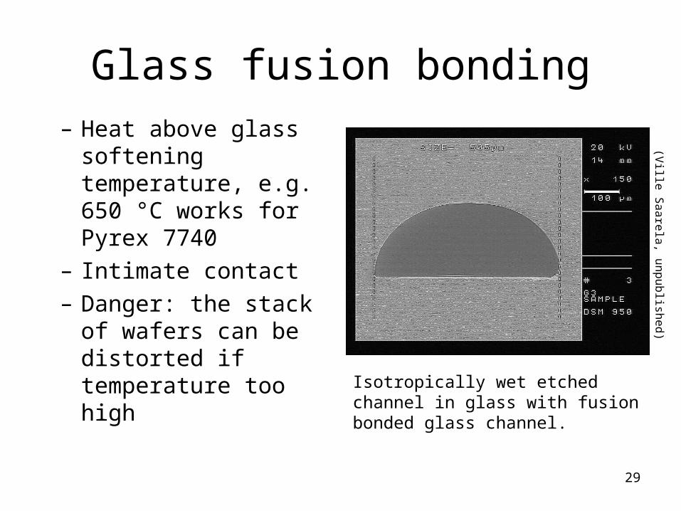
Glass fusion bonding– Heat above glass
softening temperature, e.g. 650 °C works for Pyrex 7740
– Intimate contact– Danger: the stack of
wafers can be distorted if temperature too high
29
Isotropically wet etched channel in glass with fusion bonded glass channel.
(Ville Saarela, unpublished)
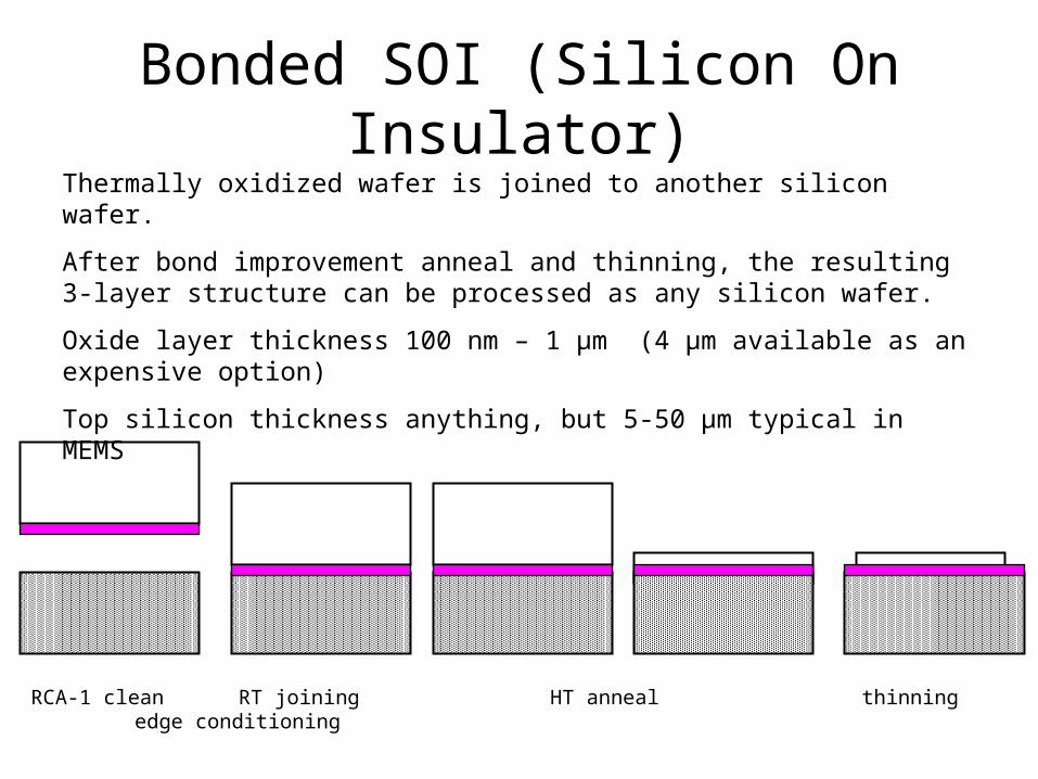
Bonded SOI (Silicon On Insulator)
RCA-1 clean RT joining HT anneal thinning edge conditioning
Thermally oxidized wafer is joined to another silicon wafer.
After bond improvement anneal and thinning, the resulting 3-layer structure can be processed as any silicon wafer.
Oxide layer thickness 100 nm – 1 µm (4 µm available as an expensive option)
Top silicon thickness anything, but 5-50 µm typical in MEMS
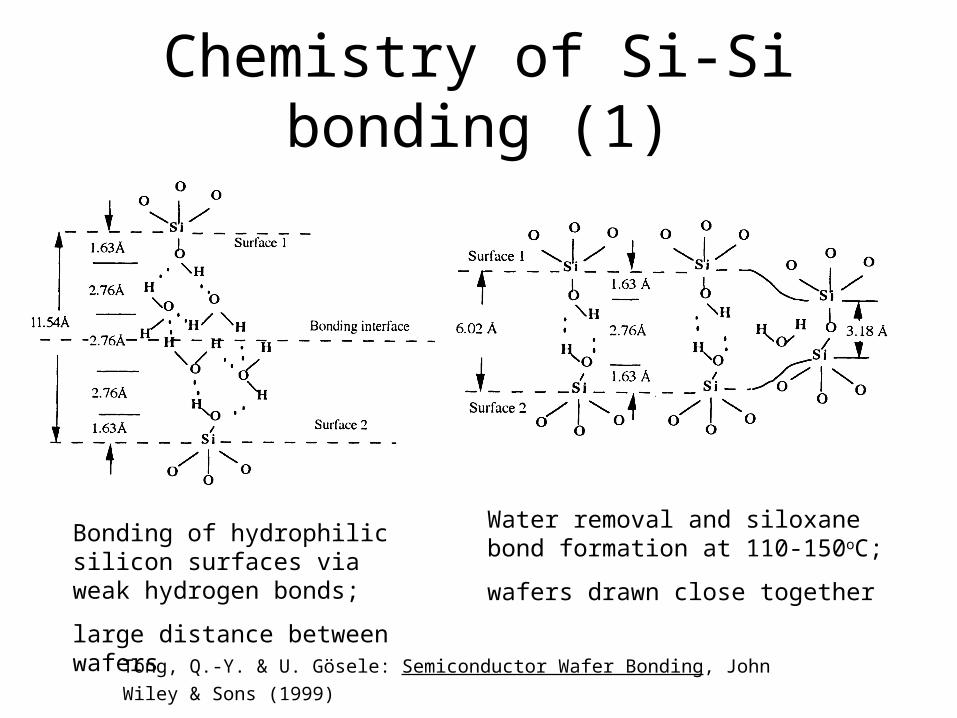
Chemistry of Si-Si bonding (1)
Water removal and siloxane bond formation at 110-150oC;
wafers drawn close together
Bonding of hydrophilic silicon surfaces via weak hydrogen bonds;
large distance between wafers
Tong, Q.-Y. & U. Gösele: Semiconductor Wafer Bonding, John Wiley & Sons (1999)
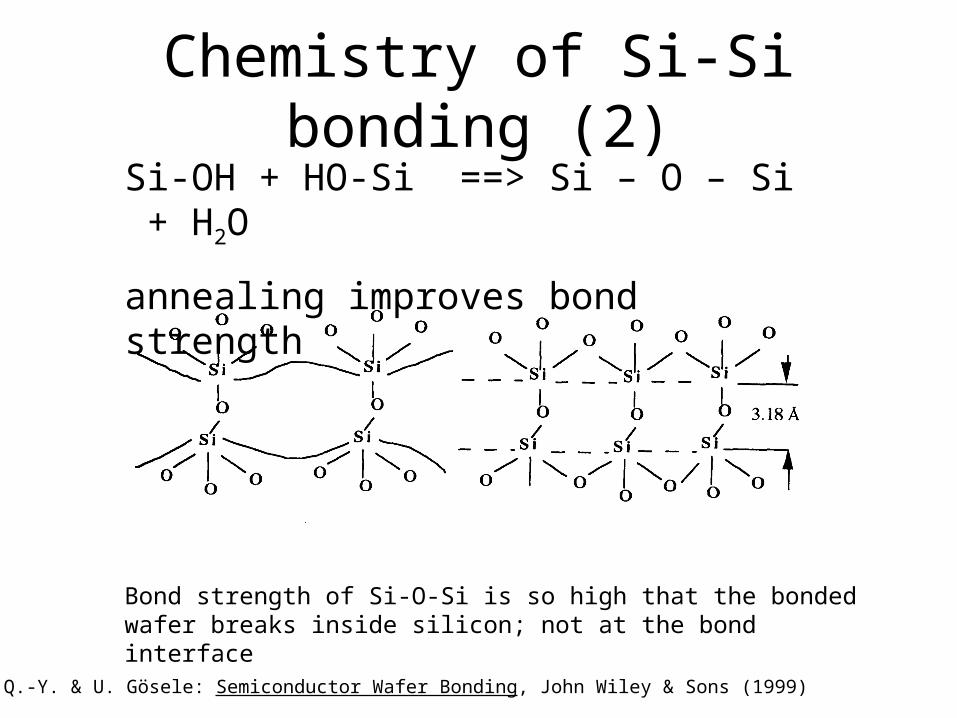
Chemistry of Si-Si bonding (2)Si-OH + HO-Si ==> Si – O – Si + H2O
annealing improves bond strength
Bond strength of Si-O-Si is so high that the bonded wafer breaks inside silicon; not at the bond interface
Tong, Q.-Y. & U. Gösele: Semiconductor Wafer Bonding, John Wiley & Sons (1999)
33
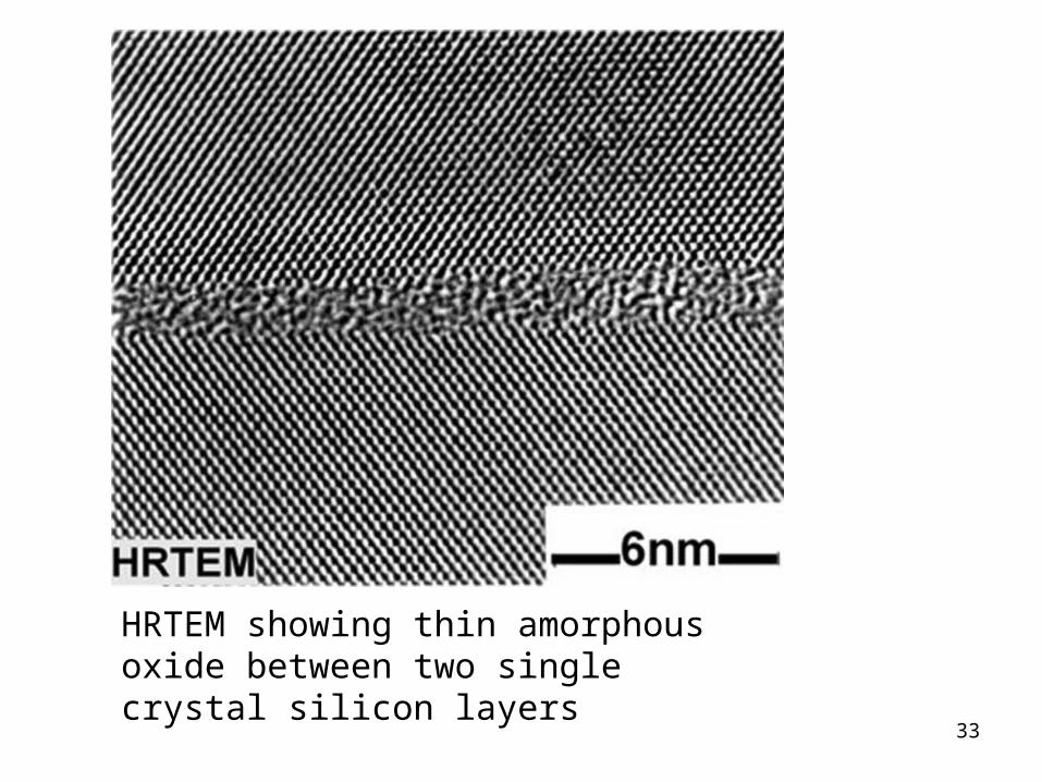
HRTEM showing thin amorphous oxide between two single crystal silicon layers
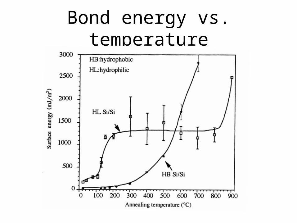
Bond energy vs. temperature
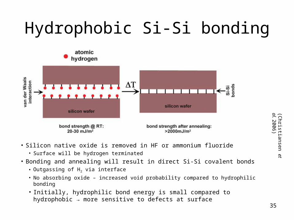
Hydrophobic Si-Si bonding
35
• Silicon native oxide is removed in HF or ammonium fluoride• Surface will be hydrogen terminated
• Bonding and annealing will result in direct Si-Si covalent bonds• Outgassing of H2 via interface
• No absorbing oxide – increased void probability compared to hydrophilic bonding
• Initially, hydrophilic bond energy is small compared to hydrophobic → more sensitive to defects at surface
(Christiansen et al. 2006)
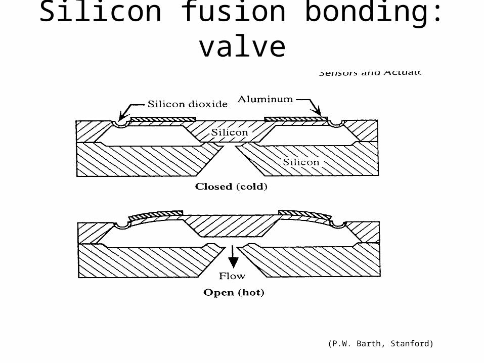
Silicon fusion bonding: valve
(P.W. Barth, Stanford)
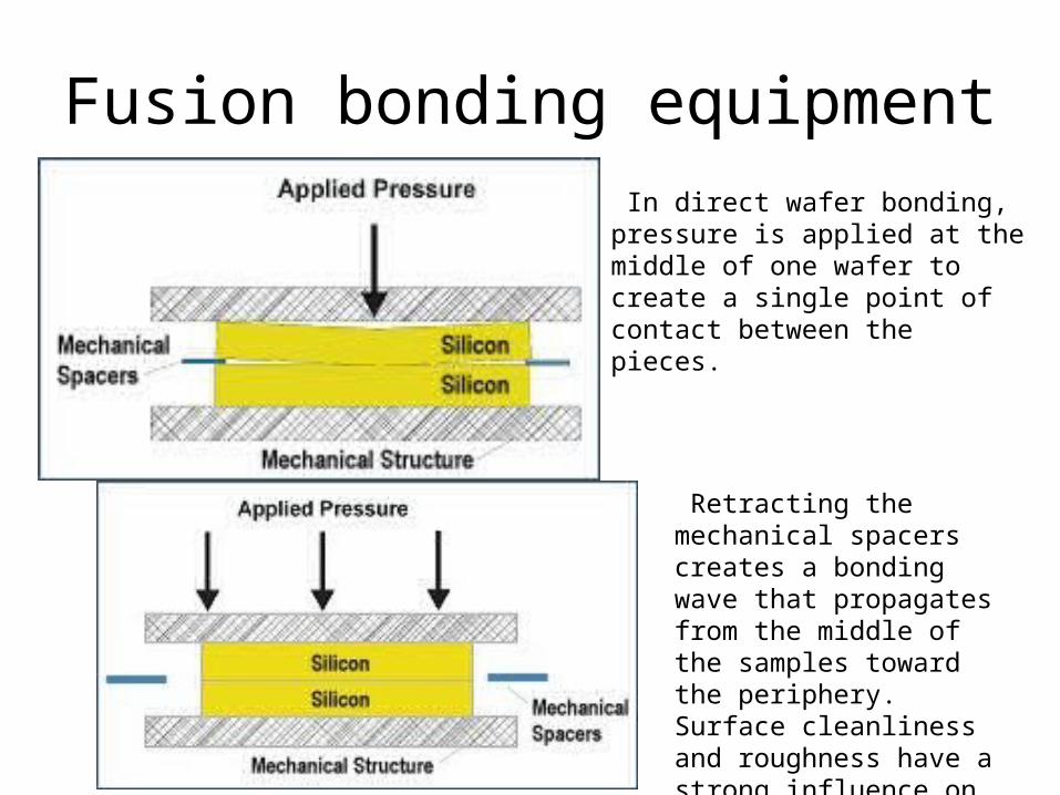
Fusion bonding equipment In direct wafer bonding, pressure is applied at the middle of one wafer to create a single point of contact between the pieces.
Retracting the mechanical spacers creates a bonding wave that propagates from the middle of the samples toward the periphery. Surface cleanliness and roughness have a strong influence on the quality of the bond.
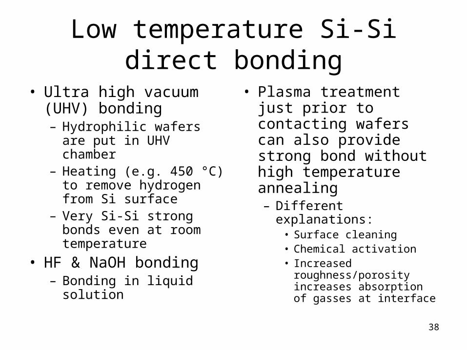
Low temperature Si-Si direct bonding
• Ultra high vacuum (UHV) bonding– Hydrophilic wafers are
put in UHV chamber– Heating (e.g. 450 °C) to
remove hydrogen from Si surface
– Very Si-Si strong bonds even at room temperature
• HF & NaOH bonding– Bonding in liquid solution
• Plasma treatment just prior to contacting wafers can also provide strong bond without high temperature annealing– Different explanations:
• Surface cleaning• Chemical activation• Increased
roughness/porosity increases absorption of gasses at interface
38
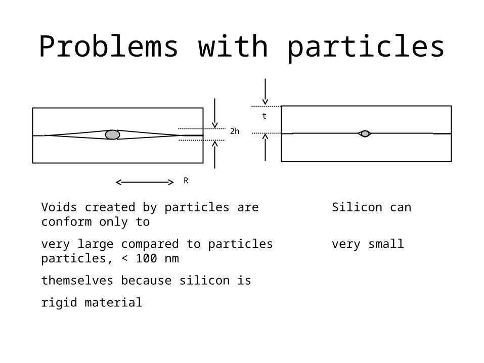
Problems with particles
R
2h
t
Voids created by particles are Silicon can conform only to
very large compared to particles very small particles, < 100 nm
themselves because silicon is
rigid material
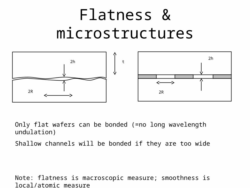
Flatness & microstructures
2h
2R 2R
2ht
Only flat wafers can be bonded (=no long wavelength undulation)
Shallow channels will be bonded if they are too wide
Note: flatness is macroscopic measure; smoothness is local/atomic measure
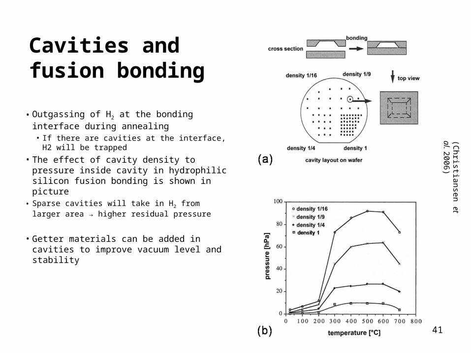
Cavities and fusion bonding
• Outgassing of H2 at the bonding interface during annealing• If there are cavities at the interface, H2 will
be trapped
• The effect of cavity density to pressure inside cavity in hydrophilic silicon fusion bonding is shown in picture
• Sparse cavities will take in H2 from larger area → higher residual pressure
• Getter materials can be added in cavities to improve vacuum level and stability
41
(Christiansen et al. 2006)
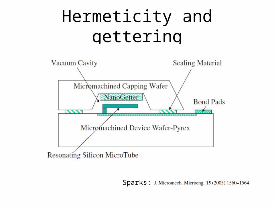
Hermeticity and gettering
Sparks:
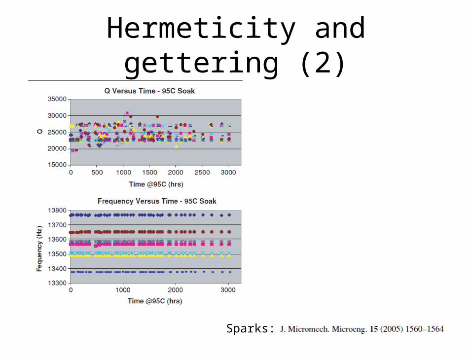
Hermeticity and gettering (2)
Sparks:
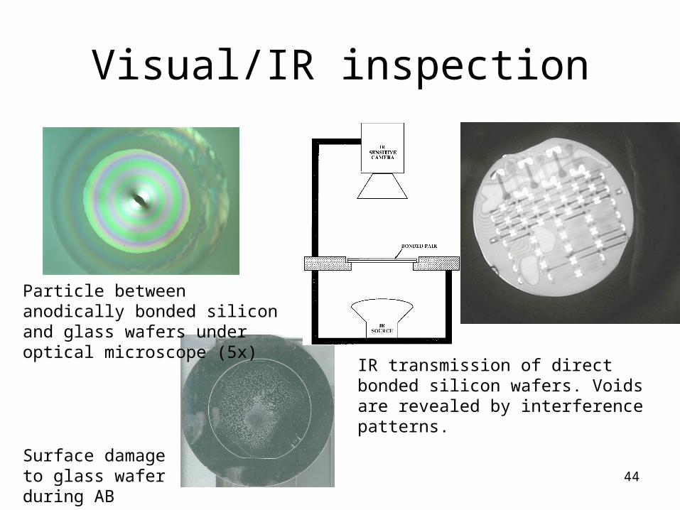
Visual/IR inspection
44
IR transmission of direct bonded silicon wafers. Voids are revealed by interference patterns.
Particle between anodically bonded silicon and glass wafers under optical microscope (5x)
Surface damage to glass wafer during AB
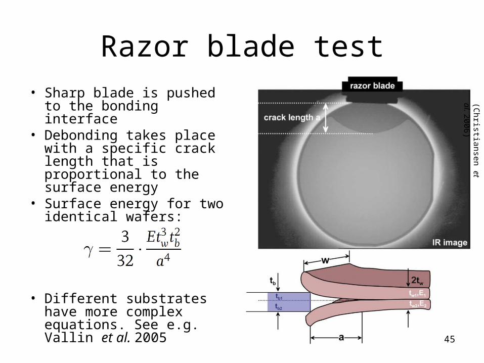
Razor blade test
• Sharp blade is pushed to the bonding interface
• Debonding takes place with a specific crack length that is proportional to the surface energy
• Surface energy for two identical wafers:
• Different substrates have more complex equations. See e.g. Vallin et al. 2005
45
(Christiansen et al. 2006)
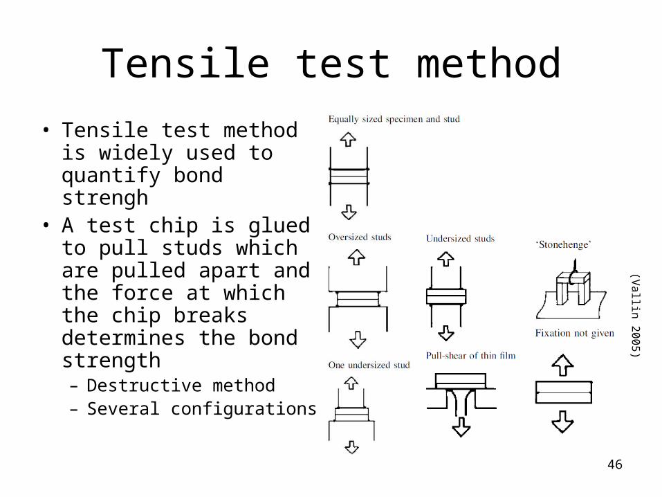
Tensile test method
• Tensile test method is widely used to quantify bond strengh
• A test chip is glued to pull studs which are pulled apart and the force at which the chip breaks determines the bond strength– Destructive method– Several configurations
46
(Vallin 2005)
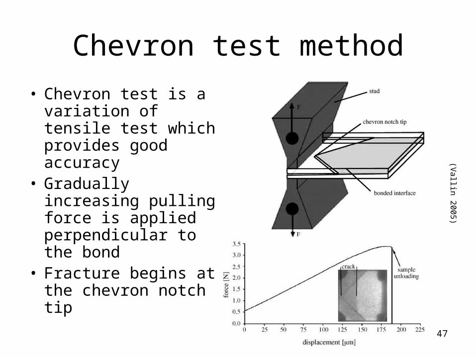
Chevron test method
• Chevron test is a variation of tensile test which provides good accuracy
• Gradually increasing pulling force is applied perpendicular to the bond
• Fracture begins at the chevron notch tip
47
(Vallin 2005)
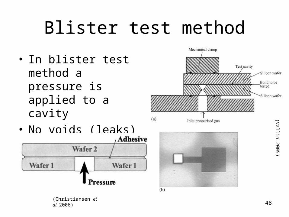
Blister test method
• In blister test method a pressure is applied to a cavity
• No voids (leaks) allowed in the studies cavity
48(Christiansen et al. 2006)
(Vallin 2005)
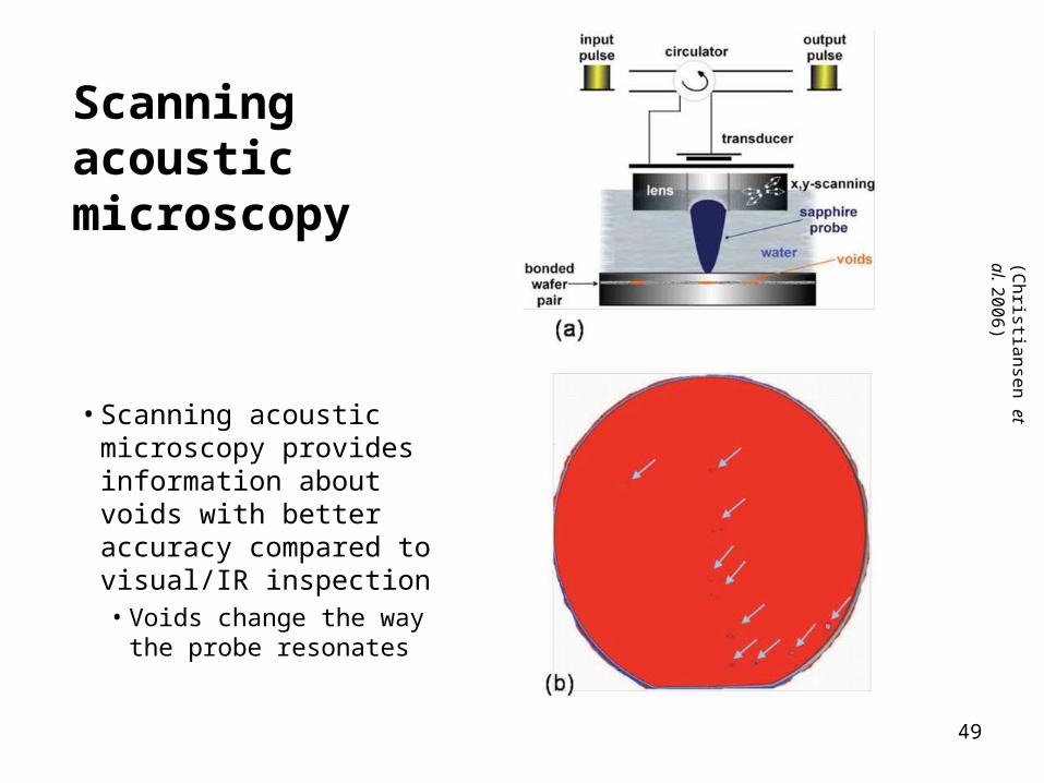
Scanning acoustic microscopy
• Scanning acoustic microscopy provides information about voids with better accuracy compared to visual/IR inspection• Voids change the way the
probe resonates
49
(Christiansen et al. 2006)
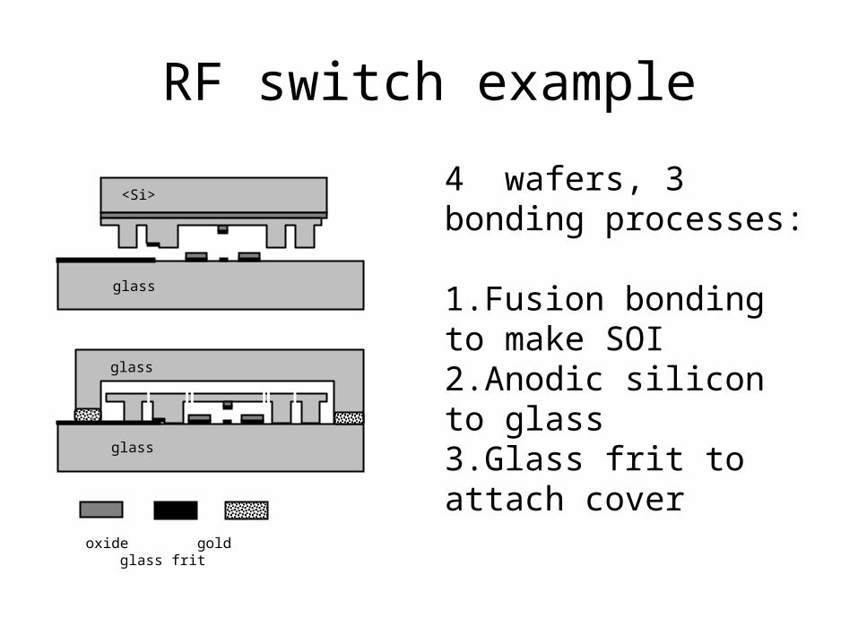
RF switch example
oxide gold glass frit
glass
<Si>
glass
glass
4 wafers, 3 bonding processes:
1.Fusion bonding to make SOI2.Anodic silicon to glass3.Glass frit to attach cover