Embed Size (px)
Citation preview
NbN superconducting nanowire single photon detector with efficiency over 90% at 1550
nm wavelength operational at compact cryocooler temperature
W. J. Zhang, L. X. You*, H. Li, J. Huang, C. L. Lv, L. Zhang, X. Y. Liu, J. J. Wu, Z. Wang and X. M.
Xie
State Key Lab of Functional Materials for Informatics,
Shanghai Institute of Microsystem and Information Technology (SIMIT), Chinese Academy of
Sciences (CAS), Shanghai, 200050, P. R. China
CAS Center for Excellence in Superconducting Electronics (CENSE)
865 Changning Rd., Shanghai, 200050, P. R. China.
Abstract
The fast development of superconducting nanowire single photon detector (SNSPD) in the past
decade has enabled many advances in quantum information technology. The best system
detection efficiency (SDE) record at 1550 nm wavelength was 93% obtained from SNSPD
made of amorphous WSi which usually operated at sub-kelvin temperatures. We first
demonstrate SNSPD made of polycrystalline NbN with SDE of 90.2% for 1550 nm wavelength
at 2.1K, accessible with a compact cryocooler. The SDE saturated to 92.1% when the
temperature was lowered to 1.8K. The results lighten the practical and high performance
SNSPD to quantum information and other high-end applications.
Main text
Single photon detector with high detection efficiency is the key enabling technology for
quantum information and various applications, such as the test of the loophole-free Bell
inequality violation1, quantum teleportation2, measurement-device-independent quantum key
distribution3, and linear optical quantum computation4. Superconducting single photon detectors
outperform the semiconducting counterparts in terms of not only detection efficiency, but also
dark count rate, timing jitter and counting rate5. As for the telecommunication wavelength 1550
nm, two records of highest system detection efficiency (SDE) over 90% were reported for two
types of detectors. One is transition edge sensor (TES) made of tungsten (W) with SDE of 95%6,
the other is superconducting nanowire single photon detector (SNSPD) made of amorphous
WSi with SDE of 93%7. However, due to the low superconducting transition temperature of the
materials W and WSi, the requirement of sub-kelvin cryogenics turns to be an inescapable
burden for practical applications. Many studies were focused on SNSPDs with different
materials aiming to obtaining high SDE at higher operating temperatures8-11, but unsuccessfully.
Regarding to another important parameter, timing jitter, WSi SNSPD and W TES have the
values of ~150 ps and 50-100 ns respectively, which limits the application requiring smaller
timing jitter.
The SDE of SNSPD (ηSDE) can be expressed as the product of three contributions7:
ηSDE=ηoc×ηabs×ηint, where ηoc is the optical coupling efficiency between the incident photons and
active area, ηabs is the absorption efficiency of nanowires and ηint is the intrinsic detection
efficiency (IDE) which describe the pulse generation probability of the nanowire when a photon
is absorbed. In order to achieve a high SDE, one has to maximize all the three parameters
simultaneously. ηoc is mainly determined by the size of the active area of SNSPD when the
optical alignment method is fixed. The impact factors of ηabs includes the geometric and optical
parameters of the nanowire (thickness, width, filling ratio, refractive index) and the optical
absorption enhancement structures (cavity). ηint is mainly determined by the superconductivity
of the nanowire. However, the factors are complicated12-14. On one hand, the geometric
parameters such as width, thickness of the nanowire play important roles. On the other hand,
the operation parameters (bias current, operation temperature) may control the ηint directly.
Besides, the uniformity of the nanowire (thickness variation, physical constrictions) handicaps
ηint since it will suppress the maximum bias current. The above analysis indicates that ηabs and
ηint are not independent, which are both related to the thickness and width of the nanowire. The
correlation between ηabs and ηint makes the improvement of SDE complicated. Indeed, it is
relatively simple for WSi SNSPD to reach high SDE since ηint can easily reach 100% with a
wide range of nanowire thickness and width due to the lower pair-breaking energy of WSi. In
the case of NbN SNSPD, it turns to be challenging since pair-breaking energy of NbN is nearly
doubled and the room for tuning those parameters is very limited.
SNSPD made of NbN is a promising choice for practical application due to its high critical
temperature, which gave the possibility of using the compact cryocooler for operation.
Unfortunately, the highest SDE reported for the NbN SNSPD are less than 80% for 1550 nm
wavelength15-17. Suspicion exists whether NbN is a candidate material for fabricating SNSPD
with SDE over 90%.
In this manuscript, we answered the suspicion by demonstrating NbN SNSPD with SDE over
90% at 1550 nm wavelength. We introduced a DBR mirror on the Si substrate, with a measured
reflectance of over 99.9% and a calculated absorption of the nanowire over 99%. The excellent
front-side single-mode lens fiber coupling is guaranteed by a large sensitive area (over 15
m). By tuning the film thickness, we were able to maximize the ηabs and ηint simultaneously.
Measured with a dilution refrigerator, the saturated SDE reaches 92.1% when the temperature
is lower than 1.8K. At 2.1K, the measured SDE is 90.2% at the dark count rate of 10 Hz, which
is further verified by cooling SNSPD using a compacted Gifford-Mcmahon (G-M) cryocooler.
Besides, due to the high switching current of NbN SNSPD, a timing jitter of 79 ps was obtained.
Results
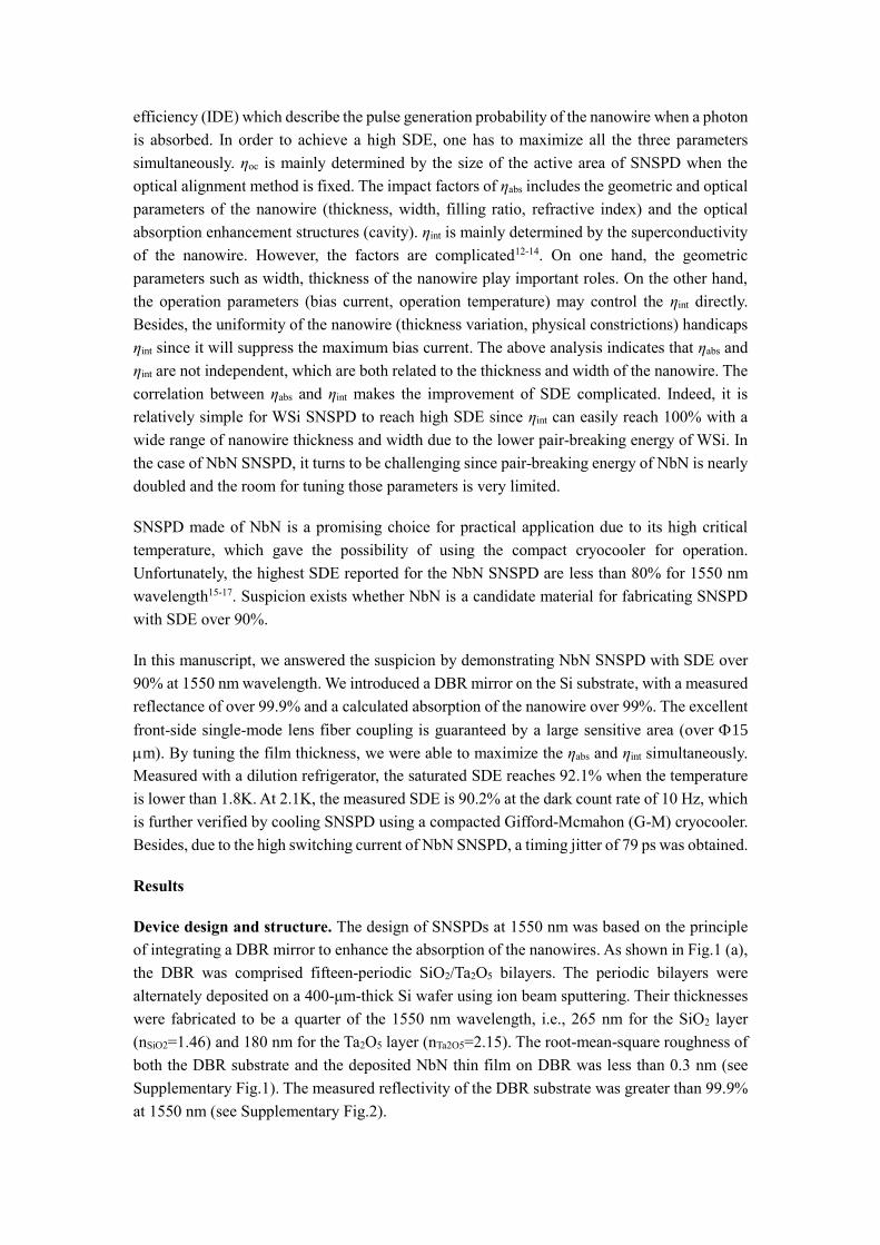
Device design and structure. The design of SNSPDs at 1550 nm was based on the principle
of integrating a DBR mirror to enhance the absorption of the nanowires. As shown in Fig.1 (a),
the DBR was comprised fifteen-periodic SiO2/Ta2O5 bilayers. The periodic bilayers were
alternately deposited on a 400-μm-thick Si wafer using ion beam sputtering. Their thicknesses
were fabricated to be a quarter of the 1550 nm wavelength, i.e., 265 nm for the SiO2 layer
(nSiO2=1.46) and 180 nm for the Ta2O5 layer (nTa2O5=2.15). The root-mean-square roughness of
both the DBR substrate and the deposited NbN thin film on DBR was less than 0.3 nm (see
Supplementary Fig.1). The measured reflectivity of the DBR substrate was greater than 99.9%
at 1550 nm (see Supplementary Fig.2).
The nanowire linewidth was empirically designed to be 75 nm to enhance its ηint. With the
linewidth fixed, numerical simulations with variable parameters, like the filling factors,
thickness and configuration of cavity, were systematically investigated before the fabrications
(see Supplementary Fig.3). The simulations indicated that a maximum absorption efficiency of
over 99% can be realized with an NbN thickness of ~7 nm, with filling factor of ~0.5, when
integrated in a half-cavity (DBR/NbN/Air).
To experimentally valid the simulations, we prepared devices with various filling factors (0.58–
0.33), and different film thicknesses (6.5–8.0 nm), covering two types of active areas (Φ15 and
18 μm). The scanning electron microscopy (SEM) images of the nanowire with a nominal 75-
nm width and 140-nm pitch is shown in Fig. 1(b), demonstrating a good controllability of the
fabrication process. Figure 1(c) shows the TEM image of the DBR mirror. The measured
thicknesses of deposited bilayers were found with ±4 nm variation from the design values.
Figure 1(d) shows a close-up TEM image of a cross-section of a nominal 7-nm-thick, 75-nm-
wide nanowire, which has a slightly trapezoid shape due to the side-etching. The TEM image
gave an estimated thickness of ~8 nm, which includes an oxidized layer (1~2 nm thick) on the
top18.
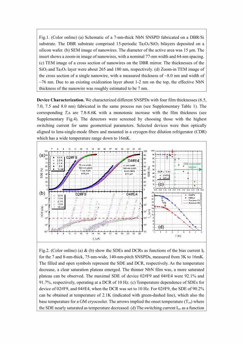
Fig.1. (Color online) (a) Schematic of a 7-nm-thick NbN SNSPD fabricated on a DBR/Si
substrate. The DBR substrate comprised 15-periodic Ta2O5/SiO2 bilayers deposited on a
silicon wafer. (b) SEM image of nanowires. The diameter of the active area was 15 μm. The
insert shows a zoom-in image of nanowires, with a nominal 77-nm width and 64-nm spacing.
(c) TEM image of a cross section of nanowires on the DBR mirror. The thicknesses of the
SiO2 and Ta2O5 layer were about 265 and 180 nm, respectively. (d) Zoom-in TEM image of
the cross section of a single nanowire, with a measured thickness of ~8.0 nm and width of
~76 nm. Due to an existing oxidization layer about 1-2 nm on the top, the effective NbN
thickness of the nanowire was roughly estimated to be 7 nm.
Device Characterization. We characterized different SNSPDs with four film thicknesses (6.5,
7.0, 7.5 and 8.0 nm) fabricated in the same process run (see Supplementary Table 1). The
corresponding Tcs are 7.8-8.6K with a monotonic increase with the film thickness (see
Supplementary Fig.4). The detectors were screened by choosing those with the highest
switching current for same geometrical parameters. Selected devices were then optically
aligned to lens-single-mode fibers and mounted in a cryogen-free dilution refrigerator (CDR)
which has a wide temperature range down to 16mK.
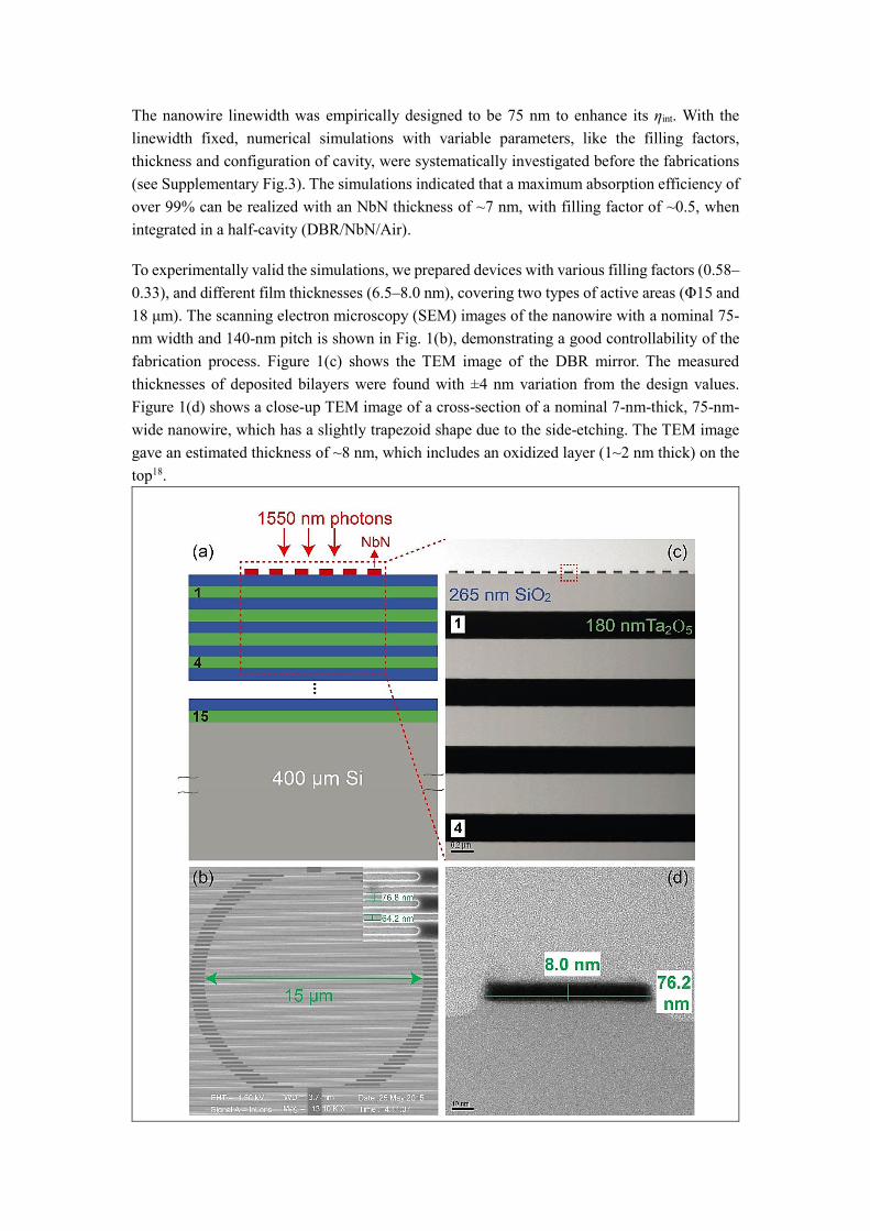
Fig.2. (Color online) (a) & (b) show the SDEs and DCRs as functions of the bias current Ib
for the 7 and 8-nm-thick, 75-nm-wide, 140-nm-pitch SNSPDs, measured from 3K to 16mK.
The filled and open symbols represent the SDE and DCR, respectively. As the temperature
decrease, a clear saturation plateau emerged. The thinner NbN film was, a more saturated
plateau can be observed. The maximal SDE of device 02#F9 and 04#E4 were 92.1% and
91.7%, respectively, operating at a DCR of 10 Hz. (c) Temperature dependence of SDEs for
device of 02#F9, and 04#E4, when the DCR was set to 10 Hz. For 02#F9, the SDE of 90.2%
can be obtained at temperature of 2.1K (indicated with green-dashed line), which also the
base temperature for a GM cryocooler. The arrows implied the onset temperature (Tos) where
the SDE nearly saturated as temperature decreased. (d) The switching current Isw as a function

of temperature for the device 02#F9 and 04#E4.
Figure 2(a) and (b) show the SDEs for 1550 nm wavelength and DCRs as functions of the bias
current Ib for two devices 02#F9 (7-nm-thick) and 04#E4 (8-nm-thick) at various temperatures.
For clarity, five curves at five temperatures (3.0, 2.5, 2.1, 1.5K, and 16mK) were displayed. In
the DCR measurement, the optical fiber port at room temperature was shielded to eliminate any
stray light from the environment. By decreasing the operation temperature, the SDE increased
and a saturation plateau appeared. When the temperature was lower than 3K, all the SDE(Ib)
curves nearly overlapped at the same bias current. At the temperature of 1.5K and lower, we
observed the highest SDE value of 92.1% for device 02#F9 at a DCR of 10 Hz and the saturation
plateau indicating that the ηint reached ~100%. When the temperature increased to 2.1K (the
lowest temperature a commercial compacted G-M cryocooler may reach), the SDE of 90.2%
can be obtained with a DCR of 10 Hz. For a 8 nm-thick NbN SNSPD (04#E4), it has a larger
switching current (Isw) of 22.5 μA compared to device 02#F9 with Isw of 15.2 μA, and the highest
SDE of 91.7% was measured at the DCR of 10 Hz at 16 mK. However, the SDE was decreased
to 76.5% at 2.1K due to the weak saturation of SDE. To further verify high SDE over 90% at
2.1K, the SDE of device 02#F9 cooled with a G-M cryocooler (base temperature of 2.13K) was
further examined using a G-M cryocooler (2.13K), which gave the value of 90.1% at DCR of
10 Hz (see Supplementary Fig.6). To the best of our knowledge, this is the first report for NbN
SNSPD with SDE over 90%. More importantly, it was realized using the G-M cryocooler
(~2.1K), which provides a practical and affordable solution of single photon detection for
quantum information.
The DCR increased monotonously with Ib at all temperatures. Two different regions can be
clearly distinguished, which are background blackbody-radiation dominated DCR (low bias
zone) and intrinsic vortex-related DCR (high bias zone). The intrinsic DCR logarithmically
increased with Ib, which shifted to the high bias current with increase/decrease of
Isw/temperature. Its onset Ib depends on the temperature. For example, at the lowest temperature
of 16mK for device 02#F9 (04#E4), the onset Ib was suppressed to 0.95(0.97)Isw, while it was
0.89(0.92)Isw at 3K. On the other hand, the background DCR curves followed the same curve
but the highest background DCR slightly increased due to the increase/decrease of
Isw/temperature. The same background DCR value at the bias current can be explained by the
consistent SDE at the same bias current and stable background blackbody radiation.
Figure 2(c) shows temperature dependence of SDEs for device of 02#F9 and 04#E4 at DCR of
10 Hz. The green-dashed line indicates the lowest temperature that a commercial G-M
cryocooler may reach directly (for example, SHI RDK-101D from Sumitomo Inc.16, 19). For
both devices, the SDE increased with a decrease of the temperature, and saturated at low
temperatures. The onset temperature (Tos) where SDE reaches its saturation as temperature
decreases was indicated with the arrow in the figure. The Tos of 02#F9 and 04#E4 were 1.8K
and 1.3K, respectively. Due to the wide saturated plateau, the SDE(T) of 02#F9 demonstrates
a slow decrease as the temperature increased, in contrast to the one of 04#E4. The different
saturation behavior was due to the film thickness difference, which will be discussed later.
Figure 2(d) shows the temperature dependence of Isws for device of 02#F9 and 04#E4. The Isw

had a measurement error about ±0.05 μA. When the temperature was lower than Tos, the Isw
gradually reached a maximum. The Isws at Tos were equaled to 14.5 and 21.9 μA, respectively.
A fitting based the Bardeen model20 simplified as Icd=α(1-(T/Tc)2)3/2 was applied to the
measured Isws and plotted as the dashed lines, where α and Tc were the variable parameters. The
fitting is consistent with the measured data well except with a slight deviation at the low
temperature region (T < 1K). Since the existence of possible constrictions in the nanowire
which may limit the experimental maximal Isw, it was expected that the measured Isw could be
smaller than the calculated depairing current Icd.
To experimentally study the performance of the optical design, we measured the wavelength
dependence of the maximum SDE// and SDE⏊ when the polarization of the photons is parallel
and vertical to the direction of the nanowire. For comparison, the simulated absorption A is also
given from 1200 to 1800 nm. As shown in Fig.3, the absorption A// showed a broad peak with
a value of 99.5% (98.1%) for 7(8) nm thick nanowire at wavelength around 1550 nm. The
measured SDE//s are roughly 7% lower than the calculated absorption while SDE⏊s are ~6%
higher than the corresponding calculated absorption. In other words, the measured polarization
extinction ratio (PER, defined as SDE///SDE⏊) is lower than the calculated PER (defined as
A///A⏊). For example, for 7(8)-nm-thick device, the experimental PER of 3.5(3.2) at 1550 nm
was lower than the calculated one of 4.4(4.6). The deviation indicated that the practical device
was different from the design in geometry and/or material optical parameters. Further
optimization of the fabrication process will be helpful to further improve the consistence and
the SDE. Besides, an extra ARC upon the nanowire may suppress the PER by twice or even
more if it is necessary (see Supplementary Tab. 1). On the other hand, the SDE drops faster
than the simulated value when the wavelengths were larger than 1600 nm, which can be
explained by a non-unity ηint due to the smaller photon energy (see Supplementary Fig.8).
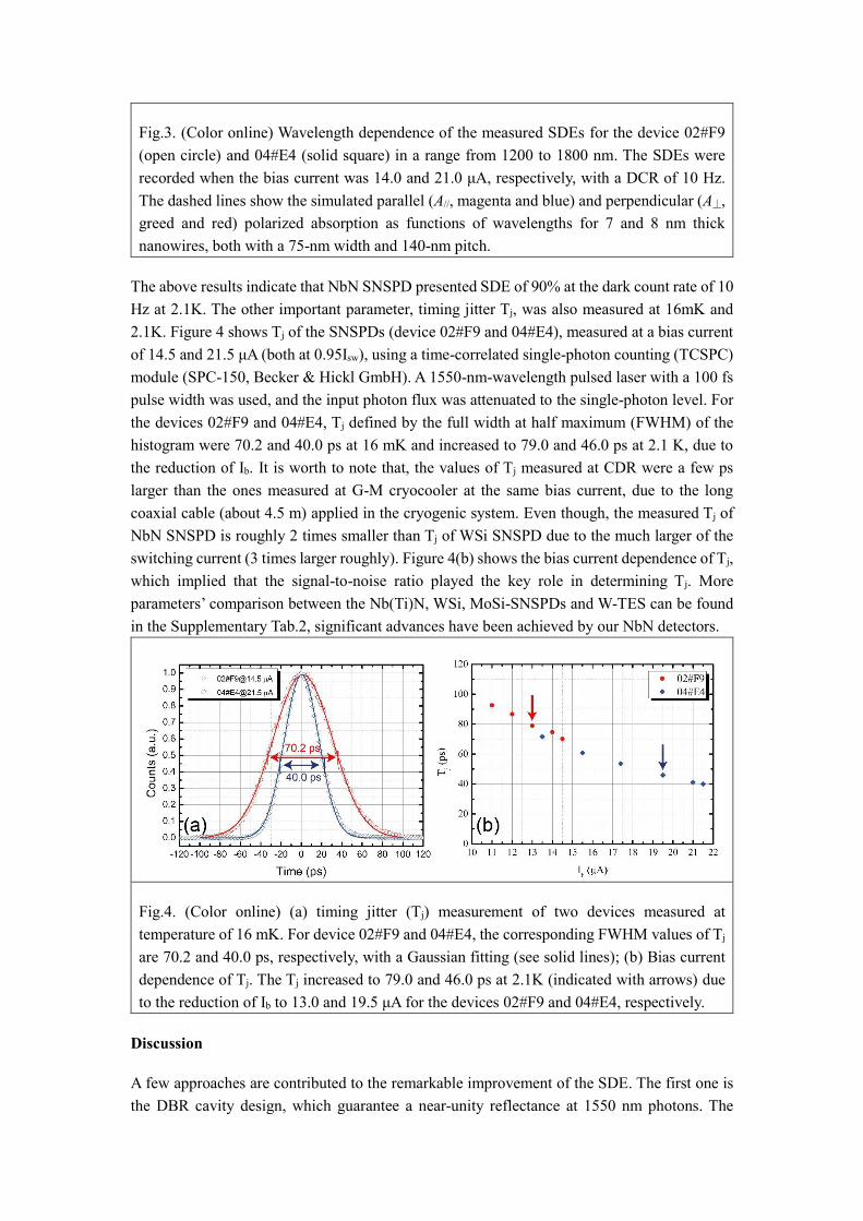
Fig.3. (Color online) Wavelength dependence of the measured SDEs for the device 02#F9
(open circle) and 04#E4 (solid square) in a range from 1200 to 1800 nm. The SDEs were
recorded when the bias current was 14.0 and 21.0 μA, respectively, with a DCR of 10 Hz.
The dashed lines show the simulated parallel (A//, magenta and blue) and perpendicular (A⏊,
greed and red) polarized absorption as functions of wavelengths for 7 and 8 nm thick
nanowires, both with a 75-nm width and 140-nm pitch.
The above results indicate that NbN SNSPD presented SDE of 90% at the dark count rate of 10
Hz at 2.1K. The other important parameter, timing jitter Tj, was also measured at 16mK and
2.1K. Figure 4 shows Tj of the SNSPDs (device 02#F9 and 04#E4), measured at a bias current
of 14.5 and 21.5 μA (both at 0.95Isw), using a time-correlated single-photon counting (TCSPC)
module (SPC-150, Becker & Hickl GmbH). A 1550-nm-wavelength pulsed laser with a 100 fs
pulse width was used, and the input photon flux was attenuated to the single-photon level. For
the devices 02#F9 and 04#E4, Tj defined by the full width at half maximum (FWHM) of the
histogram were 70.2 and 40.0 ps at 16 mK and increased to 79.0 and 46.0 ps at 2.1 K, due to
the reduction of Ib. It is worth to note that, the values of Tj measured at CDR were a few ps
larger than the ones measured at G-M cryocooler at the same bias current, due to the long
coaxial cable (about 4.5 m) applied in the cryogenic system. Even though, the measured Tj of
NbN SNSPD is roughly 2 times smaller than Tj of WSi SNSPD due to the much larger of the
switching current (3 times larger roughly). Figure 4(b) shows the bias current dependence of Tj,
which implied that the signal-to-noise ratio played the key role in determining Tj. More
parameters’ comparison between the Nb(Ti)N, WSi, MoSi-SNSPDs and W-TES can be found
in the Supplementary Tab.2, significant advances have been achieved by our NbN detectors.
Fig.4. (Color online) (a) timing jitter (Tj) measurement of two devices measured at
temperature of 16 mK. For device 02#F9 and 04#E4, the corresponding FWHM values of Tj
are 70.2 and 40.0 ps, respectively, with a Gaussian fitting (see solid lines); (b) Bias current
dependence of Tj. The Tj increased to 79.0 and 46.0 ps at 2.1K (indicated with arrows) due
to the reduction of Ib to 13.0 and 19.5 μA for the devices 02#F9 and 04#E4, respectively.
Discussion
A few approaches are contributed to the remarkable improvement of the SDE. The first one is
the DBR cavity design, which guarantee a near-unity reflectance at 1550 nm photons. The

second one is the front-side lens fiber alignment removes the reflection of the substrate in the
backside fiber-coupled SNSPDs. Third, the use of lens fiber guarantees better optical coupling
between the nanowire and the incident photons, due to a smaller beam size than the one of SM-
28e fiber. The third approach is to maximize the optical absorption and IDE simultaneously by
tuning the thickness with fixed nanowire linewidth. It seemed that the optimization reached
with the nominal film thickness of 7 nm. The absorption reaches the maximum while IDE is
also very close to unity even at 2.1K. For the film thickness of 8 nm, less saturated SDE
behavior was observed at 2.1K, though the maximum SDE is 91.7% at 16mK. With the thinner
film thickness of 6.5 nm, a more saturated SDE behavior was registered for SNSPD at 2.1K,
however, the highest SDE is only 82%, which indicated a low optical absorption (see
Supplementary Fig.7).
In conclusion, we successfully demonstrated that SDE of NbN SNSPD surpassed 90(92) % at
DCR of 10 Hz at 2.1(1.8)K, due to the adoption of DBR mirror and the simultaneous
maximization of the optical absorption and IDE. Besides, the NbN SNSPD featured a timing
jitter of 79 ps. We believe there are some room for further improving SDE by optimizing the
fabrication process, optical and superconducting properties of the film, going towards SDE of
near unity and higher operation temperature.
Methods
Device preparation. A series of NbN films with various nominal thicknesses from 6.5 nm to 8
nm were deposited onto the 2 inch DBR wafers at room temperature. The deposition of NbN
thin film were performed in a reactive direct-current magnetron sputtering system when the
partial pressures of the Ar–N2 gas mixture were 79% and 21%, respectively. The thickness of
the film was controlled by the sputtering time and verified by the XRD analysis. Then, the NbN
film was patterned into a meandered nanowire structure using electron beam lithography (EBL)
with a positive-tone ZEP520A electron-beam resist and was reactively etched in CF4 plasma.
The width of nanowire was fabricated to ~75 nm with different pitch of 130, 140, 160, 180,
200, and 230 nm. Finally, a 50-Ω-matched coplanar waveguide was formed using ultraviolet
lithography and reactive ion etching. The active areas of SNSPDs were designed with two sizes
(15 and 18 μm), which are much larger than the 6.8-μm mode field diameter of a lens fiber
for 1550 nm. The lens fiber was designed with a focal distance~145 μm, ARC target wavelength
at 1550 nm, and reflectance less than 1%. The fiber is aligned to the center of the active area
using a microscope at room temperature, the alignment error is estimated to be 3 μm. The
devices with the lens fiber were packaged in a copper box.
Measurement setup. Figure 6 shows a schematic diagram of our measurement system
incorporating a CDR. The fiber-coupled package was mounted on an Au-plated oxygen-free
copper platform thermally connected to the mixing chamber of the CDR with a base
temperature of 10 mK. The sample temperature was indicted by a RuOx resistance thermometer
located at the bottom of mixing chamber. The dilution unit is inside a fridge dewar mounted on
a vibration-attenuated stage. The temperature was tuned using a Proportional-Integral-
Derivative (PID) controller. The temperature stability were different on varied temperature
regions: T≤1K, ±0.001K; T≦1.8K, ±0.04K; T~2K, ±0.06K; T≥2.3K, ±0.03K.

Fig.5. (Color online) Schematic diagram of an ultralow-temperature measurement system for
the SNSPDs. The SNSPDs are mounted on the plate of the mixing chamber which can easily
control the temperature from 16mK to 8K by the PID controller. Optical (represented by red
lines) and electric (represented by blue lines) components are indicated in the figure.
A spliced single-mode (SM) optical fiber and a 50- coaxial cable were connected from the
top of the fridge to the SNSPD package. The coupling loss due to the fiber splicing was typically
~0.01 dB. In order to suppress the blackbody radiation of the fiber, the SM fiber was coiled in
the mixing chamber with a diameter of about 30 mm. The optical loss due to the coils were
carefully checked and found less than 0.07 dB at 1550 nm wavelength. Two tunable-wavelength
continuous-wave (CW) laser diodes (Keysight 81970, 1465–1575 nm; Keysight 81940, 1520–
1630 nm) and a supercontinuum white light laser (NKT photonics, EXB-3) were used as the
photon sources. The input light was heavily attenuated by three cascaded attenuators so that the
photon flux at the input connector of the cryostat was single-photon level. A polarization
controller (Agilent N7786B) was inserted in front of the attenuator together with power
controller to obtain the maximum SDE. Each time of tuning the polarization, the input power
was carefully rechecked by switching the input photons to the power meter (Keysight 81624B)
port. The split ratio of the MEMS optical switch was 1:1.002±0.002, guaranteed a nearly
identical input photon number to the power meter and the SNSPD. The power calibration was
performed at a level of -38.930 ±0.006 dBm, which was at the linear region of the power meter.
Then a cascaded attenuation of -33 and -40 dB by using two attenuator was adopted to the input
photons, and a final input power reached -111.930 dBm, corresponding to a photon flux of
5104 photons/s. The linearity of the three attenuators were recalibrated by the power meter,
which were found to be 0.999 ± 0.001(see Supplementary Figure 5).
The device was current-biased through the dc arm of the bias tee. The response pulse of the
detector was readout via the ac arm of the bias tee with a room-temperature amplifier (RF Bay
Inc., LNA650) and photon counter (SRS Inc., SR400). The SDE was defined as SDE = (PCR
− DCR)/(5104), where PCR is the output pulse rate of the SNSPD.
The SDEs included all losses in the system and the overall relative errors of the SDE values

could be estimated to be 2.82%, resulting from the relative uncertainty of the power meter
calibration (2.80%)21, the uncertainty of the splitting ratio (0.20%), uncertainty of the
attenuation (0.33%), and uncertainty of the PCR (0.10%). The dominated uncertainty was from
the light power calibration, which can be further reduced by using the Agilent calibration option
C0521 or the correlated-photon-based method22.
References
1. Giustina M, et al. Significant-Loophole-Free Test of Bell's Theorem with Entangled
Photons. Physical Review Letters 115, 250401 (2015).
2. Sun Q, et al. Quantum teleportation with independent sources over an optical fibre
network. Preprint at http://arxiv.org/abs/1602.07081 (2016).
3. Tang YL, et al. Measurement-Device-Independent Quantum Key Distribution over 200
km. Phys Rev Lett 113, 190501 (2014).
4. Knill E, Laflamme R, Milburn GJ. A scheme for efficient quantum computation with linear
optics. Nature 409, 46-52 (2001).
5. Hadfield RH, Johansson G. Superconducting Devices in Quantum Optics. Springer (2016).
6. Lita AE, Miller AJ, Nam SW. Counting near-infrared single-photons with 95% efficiency.
Optics express 16, 3032-3040 (2008).
7. Marsili F, et al. Detecting single infrared photons with 93% system efficiency. Nat Photon
7, 210-214 (2013).
8. Verma VB, et al. High-efficiency superconducting nanowire single-photon detectors
fabricated from MoSi thin-films. Optics express 23, 33792-33801 (2015).
9. Dorenbos SN, et al. Low gap superconducting single photon detectors for infrared
sensitivity. Applied Physics Letters 98, 251102 (2011).
10. Engel A, et al. Tantalum nitride superconducting single-photon detectors with low cut-
off energy. Applied Physics Letters 100, 062601 (2012).
11. Yu PK, et al. Superconducting single-photon detector made of MoSi film. Superconductor
Science and Technology 27, 095012 (2014).
12. Semenov A, Engel A, Hubers HW, Il'in K, Siegel M. Spectral cut-off in the efficiency of the
resistive state formation caused by absorption of a single-photon in current-carrying
superconducting nano-strips. The European Physical Journal B 47, 495-501 (2005).
13. Marsili F, et al. Single-photon detectors based on ultranarrow superconducting nanowires.
Nano letters 11, 2048-2053 (2011).

14. Renema JJ, et al. Experimental Test of Theories of the Detection Mechanism in a Nanowire
Superconducting Single Photon Detector. Physical Review Letters 112, 117604 (2014).
15. Rosenberg D, Kerman AJ, Molnar RJ, Dauler EA. High-speed and high-efficiency
superconducting nanowire single photon detector array. Opt Express 21, 1440 (2013).
16. Yamashita T, Miki S, Terai H, Wang Z. Low-filling-factor superconducting single photon
detector with high system detection efficiency. Opt Express 21, 27177-27184 (2013).
17. Chen S, et al. Dark counts of superconducting nanowire single-photon detector under
illumination. Opt Express 23, 10786-10793 (2015).
18. Semenov A, et al. Optical and transport properties of ultrathin NbN films and
nanostructures. Physical Review B 80, 054510 (2009).
19. RDK-101D 4K Cryocooler Series, <http://www.shicryogenics.com/products/4k-
cryocoolers/rdk-101d-4k-cryocooler-series/> (2016).
20. Bardeen J. Critical Fields and Currents in Superconductors. Reviews of Modern Physics 34,
667-681 (1962).
21. See the manual of Agilent 81624B. The total uncertainty of Calibration option C01/C02
was about 2.8%, while the PTB (Technische Bundesanstalt, the German national metrology
institute) traceable calibration option C05 could reduce the uncertainty down to 0.8%.
<http://literature.agilent.com/litweb/pdf/5988-7520EN.pdf> (2016).
22. Polyakov SV, Migdall AL. High accuracy verification of a correlated-photon-based
method for determining photon-counting detection efficiency. Optics express 15, 1390-
1407 (2007).

Acknowledgments
The authors would like to thank M. Wang, ZJ. Li and B. Gao from SIMIT for technical support
of the ultra-low temperature measurement. This work was funded by the National Natural
Science Foundation of China (91121022, 61401441, & 61401443), Strategic Priority Research
Program (B) of the Chinese Academy of Sciences (XDB04010200) and the Science and
Technology Commission of Shanghai Municipality under Grant 16JC1400402.
Author contributions
W.J.Z. designed and fabricated the devices. W.J.Z. and L.X.Y. wrote the paper. L.X.Y. organized
the research. H.L. preformed numerical simulations. W.J.Z. and J.H. performed the
measurements. C.L.L helped to perform the ultra-low temperature measurement with
constructive discussions. L.Z. and J.H. provided the NbN films. X.Y.L, J.J.W, Z.W., X.M.X.
and M.H.J provided helpful discussions. All authors reviewed the manuscript.
Additional information
Competing financial interests: The authors declare no competing financial interests.
Supplementary Information
Surface morphology of the NbN films
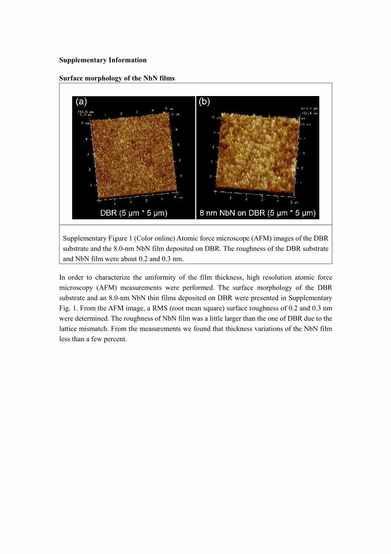
Supplementary Figure 1 (Color online) Atomic force microscope (AFM) images of the DBR
substrate and the 8.0-nm NbN film deposited on DBR. The roughness of the DBR substrate
and NbN film were about 0.2 and 0.3 nm.
In order to characterize the uniformity of the film thickness, high resolution atomic force
microscopy (AFM) measurements were performed. The surface morphology of the DBR
substrate and an 8.0-nm NbN thin films deposited on DBR were presented in Supplementary
Fig. 1. From the AFM image, a RMS (root mean square) surface roughness of 0.2 and 0.3 nm
were determined. The roughness of NbN film was a little larger than the one of DBR due to the
lattice mismatch. From the measurements we found that thickness variations of the NbN film
less than a few percent.

Measurement of reflectance of NbN film on DBR
Supplementary Figure 2. (Color online) Wavelength dependence of the reflectance of DBR
wafer (RDBR) and NbN films deposited on DBR wafer (RNbN) with thickness of 7 and 8 nm,
measured at room temperature by a spectrophotometer. At 1550 nm wavelength, the RDBR
and RNbN for 7(8) nm were 99.9% and 0.77(2.24)%, respectively. The insert shows a zoom-
in region around the minima of the RNbN for 7(8) nm.
Since the absorption A can be expressed as A = 1-Tr-R and the transmission Tr is negligible
(~0.1%) for the high reflectance mirror, the reflectance R can be directly measured by a
spectrophotometer, then A can be deduced as A ~ 1-R. Figure 4 shows the measured reflectance
as a function of wavelengths from 1200 to 1900 nm, for the NbN thin films deposited on DBR
mirror with the thickness of 7(8) nm. The reflectance minima appears around 1570-1600 nm,
implied high absorption of NbN film in these wavelengths.
The measured reflectance data shows that near-unity absorption in NbN film can be obtained
when the film thickness on the DBR mirror is about 7 nm. As the thickness increase, the
reflectance increases. However, it should be noted that, the absorption of thin film (Afilm) could
be different from the absorption of nanowire or device (Adevice), and the Afilm defines the upper
bound for Adevice.
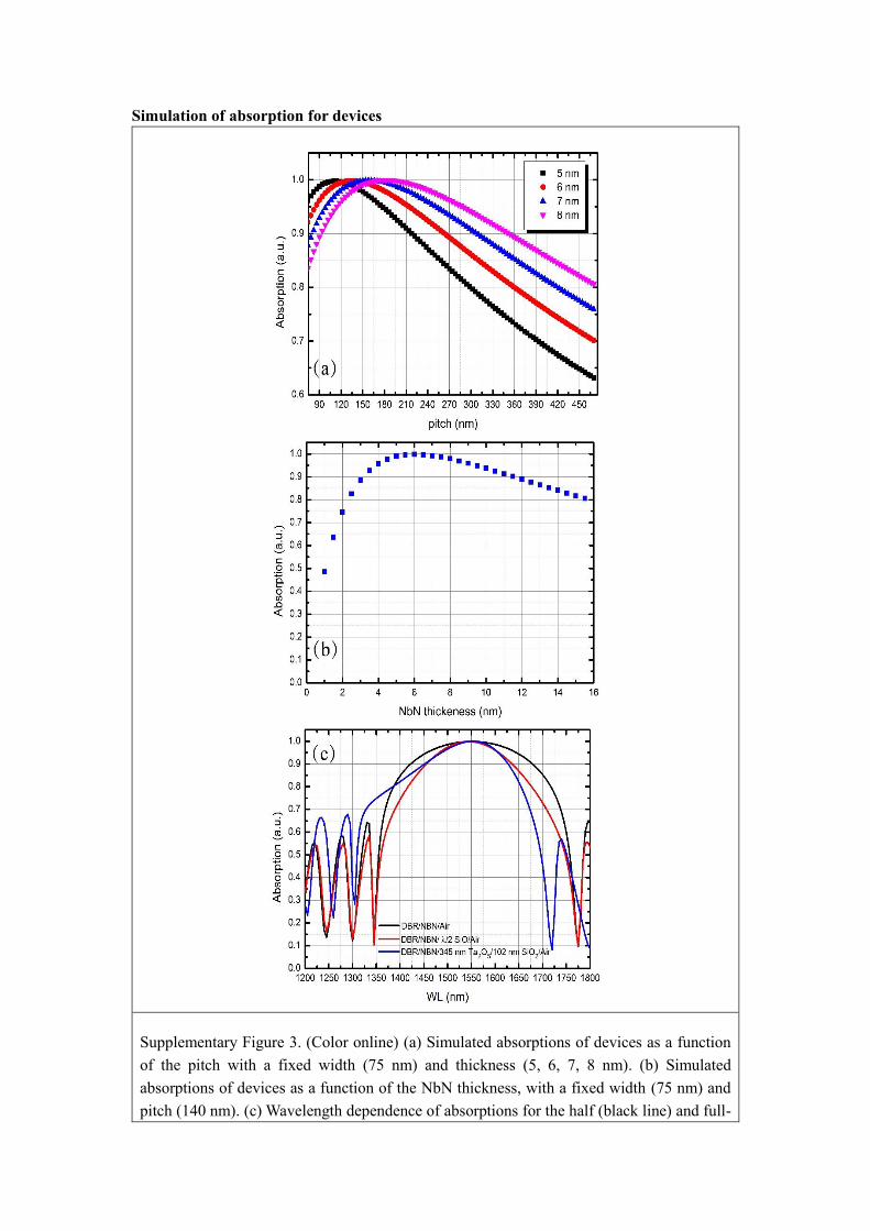
Simulation of absorption for devices
Supplementary Figure 3. (Color online) (a) Simulated absorptions of devices as a function
of the pitch with a fixed width (75 nm) and thickness (5, 6, 7, 8 nm). (b) Simulated
absorptions of devices as a function of the NbN thickness, with a fixed width (75 nm) and
pitch (140 nm). (c) Wavelength dependence of absorptions for the half (black line) and full-

cavity (red, blue and green lines) devices, with a fixed width (75 nm) and pitch (140 nm).
For the full-cavity designs, their front anti-reflection coating (ARC) were tuned with varied
dielectric materials. The introduced ARC to the half cavity design resulted in narrowing the
bandwidth.
In order to optimize the Adevice, numerical simulations were performed by the rigorous coupled-
wave analysis method. The parameters in the simulation, i.e., the refractive index of NbN, nNbN
= 6.50+5.83i, at 1550 nm was obtained using a spectroscopic ellipsometer, and the refractive
index and thickness of the Si substrate were nSi = 3.46, and L = 400 μm, respectively.
Supplementary Fig.3 (a) shows the Adevice as a function of pitch with a fixed 75-nm width for
the case at different thicknesses (5.0-8.0 nm). In the case of thickness at 7.0 nm, maxima over
99% appeared at the pitch ranging from 130 to 190 nm. As the thickness increases, the position
of the maxima shifted to a large pitch, i.e., a larger spacing is necessary for thicker film. As
shown in Supplementary Fig.3 (b), the Adevice with fixed width and pitch (75 and 140 nm) first
increased then fell gradually as the NbN thickness increased. Adevice reached a maxima over 0.99
at 5.5-7.0 nm.
Supplementary Fig.3 (c) shows the influence of the anti-reflection coating (ARC) on the half-
cavity (DBR/NbN/Air) design. The designs of ARC were tuned with several types of materials,
such as SiO (the SiO refractive index nSiO = 1.89), SiO2 and Ta2O5. It can be found that the ARC
coatings (SiO and SiO2/Ta2O5 bilayer) did not significantly change the absorption around the
target wavelengths but resulted in a reduction of bandwidth. Therefore, for a simplified
fabrication process, the half cavity design can provide a high enough absorption over 0.995.
RT measurements of the devices with various thicknesses
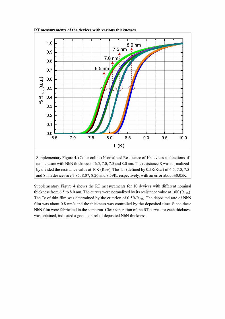
Supplementary Figure 4. (Color online) Normalized Resistance of 10 devices as functions of
temperature with NbN thickness of 6.5, 7.0, 7.5 and 8.0 nm. The resistance R was normalized
by divided the resistance value at 10K (R10K). The Tcs (defined by 0.5R/R10K) of 6.5, 7.0, 7.5
and 8 nm devices are 7.85, 8.07, 8.26 and 8.59K, respectively, with an error about ±0.05K.
Supplementary Figure 4 shows the RT measurements for 10 devices with different nominal
thickness from 6.5 to 8.0 nm. The curves were normalized by its resistance value at 10K (R10K).
The Tc of thin film was determined by the criterion of 0.5R/R10K. The deposited rate of NbN
film was about 0.8 nm/s and the thickness was controlled by the deposited time. Since these
NbN film were fabricated in the same run. Clear separation of the RT curves for each thickness
was obtained, indicated a good control of deposited NbN thickness.
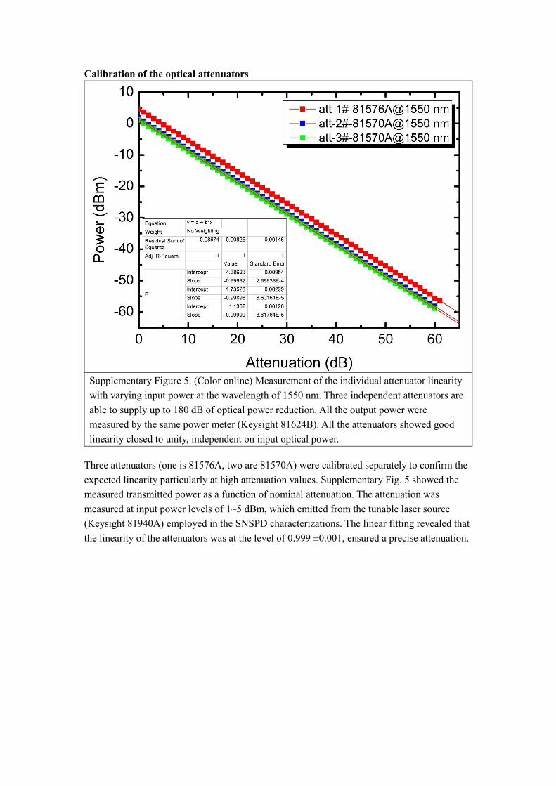
Calibration of the optical attenuators
Supplementary Figure 5. (Color online) Measurement of the individual attenuator linearity
with varying input power at the wavelength of 1550 nm. Three independent attenuators are
able to supply up to 180 dB of optical power reduction. All the output power were
measured by the same power meter (Keysight 81624B). All the attenuators showed good
linearity closed to unity, independent on input optical power.
Three attenuators (one is 81576A, two are 81570A) were calibrated separately to confirm the
expected linearity particularly at high attenuation values. Supplementary Fig. 5 showed the
measured transmitted power as a function of nominal attenuation. The attenuation was
measured at input power levels of 1~5 dBm, which emitted from the tunable laser source
(Keysight 81940A) employed in the SNSPD characterizations. The linear fitting revealed that
the linearity of the attenuators was at the level of 0.999 ±0.001, ensured a precise attenuation.
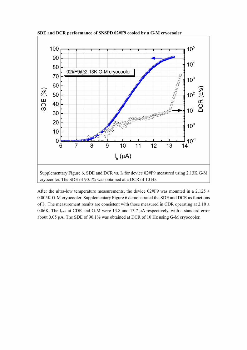
SDE and DCR performance of SNSPD 02#F9 cooled by a G-M cryocooler
Supplementary Figure 6. SDE and DCR vs. Ib for device 02#F9 measured using 2.13K G-M
cryocooler. The SDE of 90.1% was obtained at a DCR of 10 Hz.
After the ultra-low temperature measurements, the device 02#F9 was mounted in a 2.125 ±
0.005K G-M cryocooler. Supplementary Figure 6 demonstrated the SDE and DCR as functions
of Ib. The measurement results are consistent with those measured in CDR operating at 2.10 ±
0.06K. The Isws at CDR and G-M were 13.8 and 13.7 μA respectively, with a standard error
about 0.05 μA. The SDE of 90.1% was obtained at DCR of 10 Hz using G-M cryocooler.

Performance of 6.5-nm-thick devices
Supplementary Figure 7. (Color online) Parallel polarized SDE and DCR vs. Ib for the device
01#G7, with an NbN thickness of 6.5 nm, measured at 2.1 and 16mK. A clear saturation
plateau can be still observed at 2.1K, due to the reduction of thickness.
Supplementary Figure 7 shows the parallel polarized SDE and DCR as functions of Ib for the
device 01#G7, measured at 2.1 and 16mK. This device was featured with a nominal 6.5-nm
thick, 75-nm wide and 130-nm-picth nanowire, covering an active area of Φ18 μm. Its Isw of
11.2 μA at 16mK is lower than the ones described in Fig.2 (15.2 and 22.5 μA) due to the thinner
nanowire. Maximum SDE for this device was 82.2%, and the PER was 3.9 at 1550 nm. A
significantly lower SDE was obtained in the thickness of 6.5 nm, than its simulated absorption
of over 95%. This SDE was also about 10% lower than the 7(8)-nm-thick devices. We then
carefully measured other devices in the same run and found the saturated SDEs was in the range
of 70%-82%, varied by devices (Supplementary Table 1). Thus, the deviation between the
experiment and simulation could be due to the thin nanowire combined with an imperfect DBR
cavity, resulting in low photon absorption.
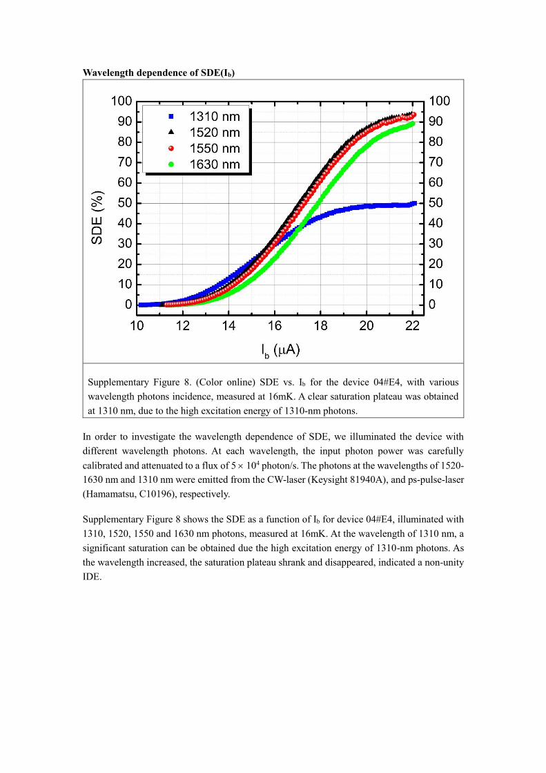
Wavelength dependence of SDE(Ib)
Supplementary Figure 8. (Color online) SDE vs. Ib for the device 04#E4, with various
wavelength photons incidence, measured at 16mK. A clear saturation plateau was obtained
at 1310 nm, due to the high excitation energy of 1310-nm photons.
In order to investigate the wavelength dependence of SDE, we illuminated the device with
different wavelength photons. At each wavelength, the input photon power was carefully
calibrated and attenuated to a flux of 5 104 photon/s. The photons at the wavelengths of 1520-
1630 nm and 1310 nm were emitted from the CW-laser (Keysight 81940A), and ps-pulse-laser
(Hamamatsu, C10196), respectively.
Supplementary Figure 8 shows the SDE as a function of Ib for device 04#E4, illuminated with
1310, 1520, 1550 and 1630 nm photons, measured at 16mK. At the wavelength of 1310 nm, a
significant saturation can be obtained due the high excitation energy of 1310-nm photons. As
the wavelength increased, the saturation plateau shrank and disappeared, indicated a non-unity
IDE.

Response pulses of photon response
Supplementary Figure 9. (Color online) Response pulses of device 02#F9 and 04#F9
recorded by an oscilloscope at Ib = 14.5 and 21 μA, respectively, when the devices operated
at 16mK. The fast decay time of device 04#E4 was due to its small active area of Φ15 μm
and thick thickness.
We characterized the decay time of the response pulse by directly monitoring the amplified
output electronic pulse with an oscilloscope. Response pulses of two devices 02#F9 and 04#F9
were shown in Supplementary Fig. 9, when the devices were biased at Ib = 14.5 and 21 μA,
respectively, and operated at 16mK. We fitted the decay time by using an exponential decay
function expressed as a + b*(e-t/τ), where τ is the time at which the height of the pulse is reduced
to 1/e = 0.368 to its initial value, a and b are fitting parameters. Thus, by the fitting the decay
part of the pulse, we obtain the decay time τ = 48.5 (27.3) ns for device 02#F9 (04#F9).
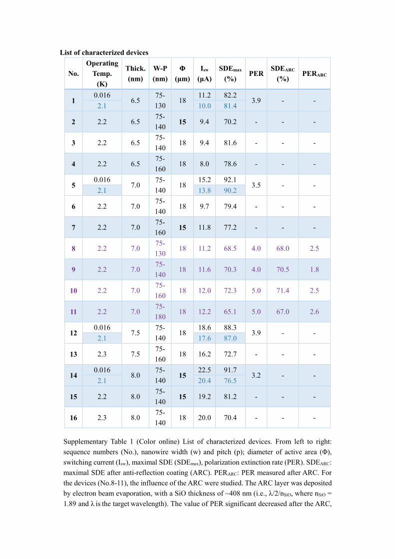
List of characterized devices
No.
Operating
Temp.
(K)
Thick.
(nm)
W-P
(nm)
Φ
(μm)
Isw
(μA)
SDEmax
(%) PER
SDEARC
(%) PERARC
1 0.016
6.5 75-
130 18
11.2 82.2 3.9 - -
2.1 10.0 81.4
2 2.2 6.5 75-
140 15 9.4 70.2 - - -
3 2.2 6.5 75-
140 18 9.4 81.6 - - -
4 2.2 6.5 75-
160 18 8.0 78.6 - - -
5 0.016
7.0 75-
140 18
15.2 92.1 3.5 - -
2.1 13.8 90.2
6 2.2 7.0 75-
140 18 9.7 79.4 - - -
7 2.2 7.0 75-
160 15 11.8 77.2 - - -
8 2.2 7.0 75-
130 18 11.2 68.5 4.0 68.0 2.5
9 2.2 7.0 75-
140 18 11.6 70.3 4.0 70.5 1.8
10 2.2 7.0 75-
160 18 12.0 72.3 5.0 71.4 2.5
11 2.2 7.0 75-
180 18 12.2 65.1 5.0 67.0 2.6
12 0.016
7.5 75-
140 18
18.6 88.3 3.9 - -
2.1 17.6 87.0
13 2.3 7.5 75-
160 18 16.2 72.7 - - -
14 0.016
8.0 75-
140 15
22.5 91.7 3.2 - -
2.1 20.4 76.5
15 2.2 8.0 75-
140 15 19.2 81.2 - - -
16 2.3 8.0 75-
140 18 20.0 70.4 - - -
Supplementary Table 1 (Color online) List of characterized devices. From left to right:
sequence numbers (No.), nanowire width (w) and pitch (p); diameter of active area (Φ),
switching current (Isw), maximal SDE (SDEmax), polarization extinction rate (PER). SDEARC:
maximal SDE after anti-reflection coating (ARC). PERARC: PER measured after ARC. For
the devices (No.8-11), the influence of the ARC were studied. The ARC layer was deposited
by electron beam evaporation, with a SiO thickness of ~408 nm (i.e., λ/2/nSiO, where nSiO =
1.89 and λ is the target wavelength). The value of PER significant decreased after the ARC,
while the SDE did not showed a notable change.
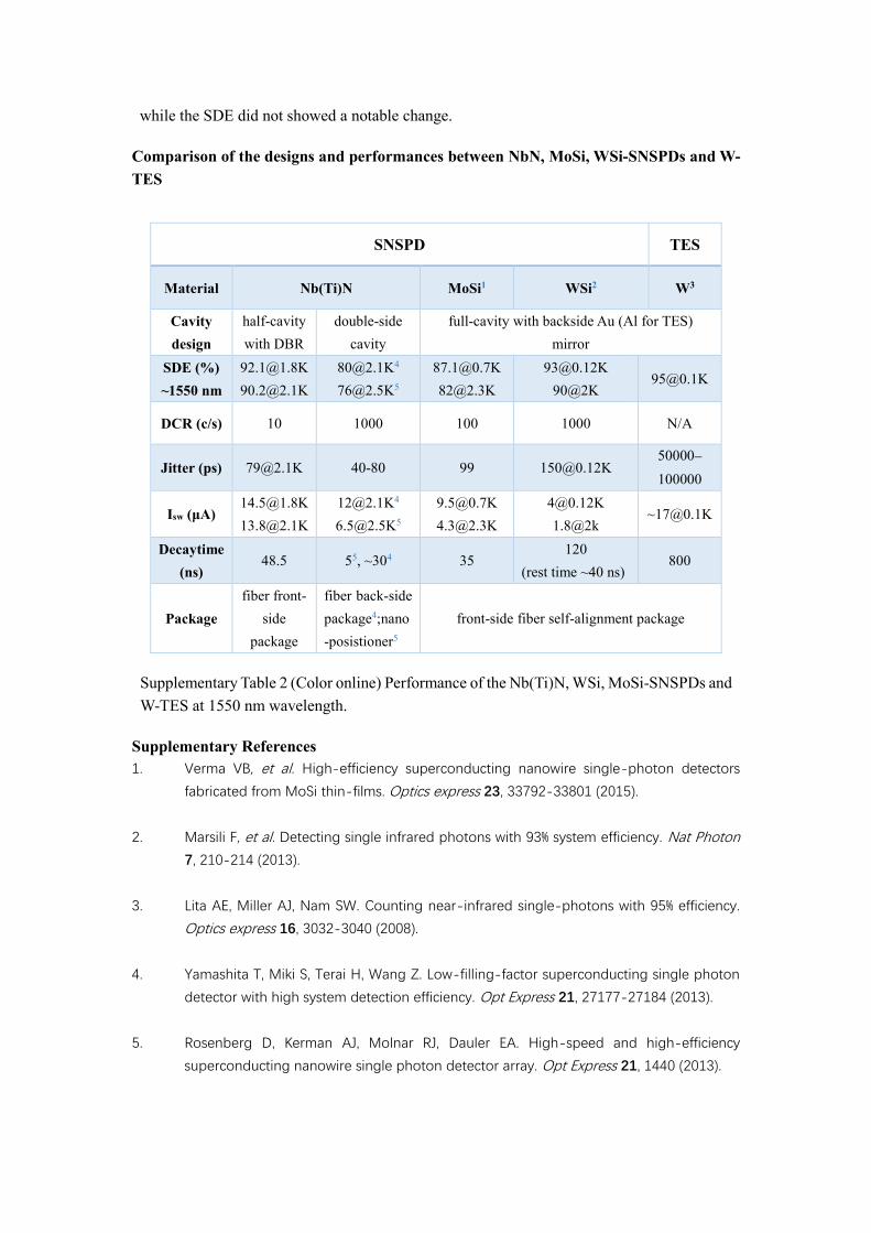
Comparison of the designs and performances between NbN, MoSi, WSi-SNSPDs and W-
TES
SNSPD TES
Material Nb(Ti)N MoSi1 WSi2 W3
Cavity
design
half-cavity
with DBR
double-side
cavity
full-cavity with backside Au (Al for TES)
mirror
SDE (%)
~1550 nm
90@2K [email protected]
DCR (c/s) 10 1000 100 1000 N/A
Jitter (ps) [email protected] 40-80 99 [email protected] 50000–
100000
Isw (μA) [email protected]
1.8@2k [email protected]
Decaytime
(ns) 48.5 55, ~304 35
120
(rest time ~40 ns) 800
Package
fiber front-
side
package
fiber back-side
package4;nano
-posistioner5
front-side fiber self-alignment package
Supplementary Table 2 (Color online) Performance of the Nb(Ti)N, WSi, MoSi-SNSPDs and
W-TES at 1550 nm wavelength.
Supplementary References
1. Verma VB, et al. High-efficiency superconducting nanowire single-photon detectors
fabricated from MoSi thin-films. Optics express 23, 33792-33801 (2015).
2. Marsili F, et al. Detecting single infrared photons with 93% system efficiency. Nat Photon
7, 210-214 (2013).
3. Lita AE, Miller AJ, Nam SW. Counting near-infrared single-photons with 95% efficiency.
Optics express 16, 3032-3040 (2008).
4. Yamashita T, Miki S, Terai H, Wang Z. Low-filling-factor superconducting single photon
detector with high system detection efficiency. Opt Express 21, 27177-27184 (2013).
5. Rosenberg D, Kerman AJ, Molnar RJ, Dauler EA. High-speed and high-efficiency
superconducting nanowire single photon detector array. Opt Express 21, 1440 (2013).